Article

Optoelectronic Properties and the Electrical Stability of Ga-Doped ZnO Thin Films Prepared via Radio Frequency Sputtering

1
Institute of Physics, Academia Sinica, Taipei 115, Taiwan
2
Institute of Optoelectronic Science, National Taiwan Ocean University, Keelung 202, Taiwan
3
Institute of Materials Science and Engineering, Ocean University of China, 238 Songling Road, Qingdao 266100, China
4
Department of Materials Engineering and Center for Thin Film Technologies and Applications, Ming Chi University of Technology, Taipei 243, Taiwan
5
Department of Electronic Engineering, Chang Gung University, Taoyuan 333, Taiwan
*
Author to whom correspondence should be addressed.
Materials 2016, 9(12), 987; https://doi.org/10.3390/ma9120987
Submission received: 26 October 2016 / Revised: 22 November 2016 / Accepted: 29 November 2016 / Published: 6 December 2016
(This article belongs to the Special Issue Advances in Transparent Conducting Materials)

Abstract

:
In this work, Ga-doped ZnO (GZO) thin films were deposited via radio frequency sputtering at room temperature. The influence of the Ga content on the film’s optoelectronic properties as well as the film’s electrical stability were investigated. The results showed that the film’s crystallinity degraded with increasing Ga content. The film’s conductivity was first enhanced due to the replacement of Zn2+ by Ga3+ before decreasing due to the separation of neutralized gallium atoms from the ZnO lattice. When the Ga content increased to 15.52 at %, the film’s conductivity improved again. Furthermore, all films presented an average transmittance exceeding 80% in the visible region. Regarding the film’s electrical stability, GZO thermally treated below 200 °C exhibited no significant deterioration in electrical properties, but such treatment over 200 °C greatly reduced the film’s conductivity. In normal atmospheric conditions, the conductivity of GZO films remained very stable at ambient temperature for more than 240 days.

Graphical Abstract

1. Introduction

Transparent conductive oxides (TCOs) have been widely studied in the last few decades due to their high electrical conductivity and good optical transmittance in the visible light region. They can be used in fields such as solar cells, flat-panel displays, light emitting diodes, and smart windows [1,2,3,4,5]. In particular, Sn-doped In2O3 (ITO) films present outstanding optoelectronic performance and have been widely used in various commercial domains [6,7,8]. However, due to the toxicity and limited availability of indium, further applications of ITO are restricted, so novel alternative materials must be developed [9,10]. ZnO-based oxides are considered one of the most promising transparent conductive oxides due to their low production cost, non-toxicity, low growth temperature, and high adaptability to various substrates [11,12,13,14,15,16]. Nevertheless, their practical feasibility is strongly restricted by the poor electrical properties of intrinsic ZnO thin films. In order to overcome this drawback, many studies have attempted to improve the performance of ZnO. One approach is to enhance the electrical and optical properties of ZnO thin films by trivalent Ga doping [17,18,19,20,21].
In this work, Ga-doped ZnO (GZO) thin films were prepared via radio frequency (rf) sputtering on ZnO and Ga2O3 targets. The influences of varying the sputtering power applied to the Ga2O3 target on the composition and optoelectronic properties of the films were investigated. The film’s thermal and time stabilities are also discussed.

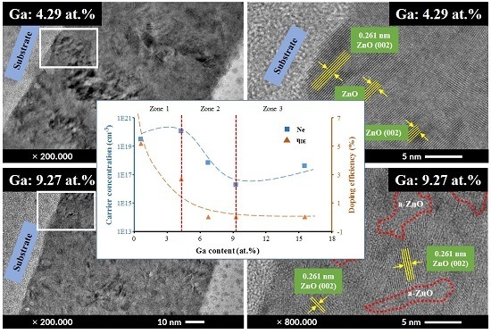
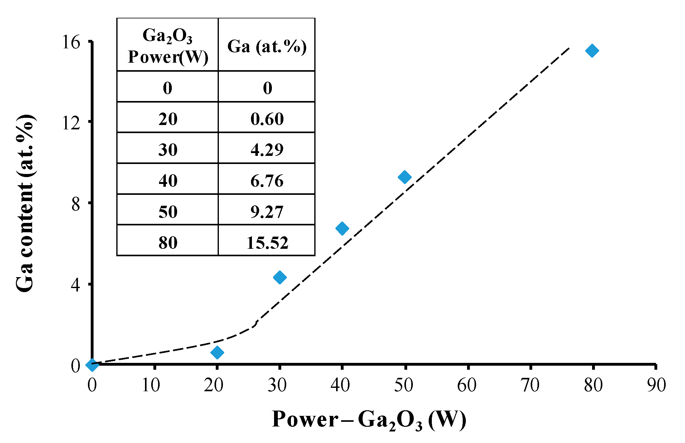
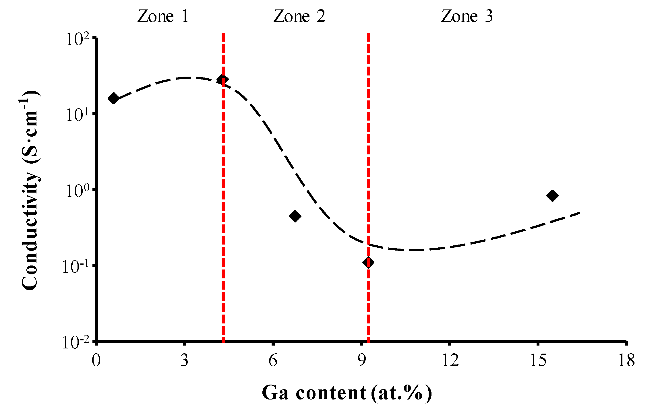
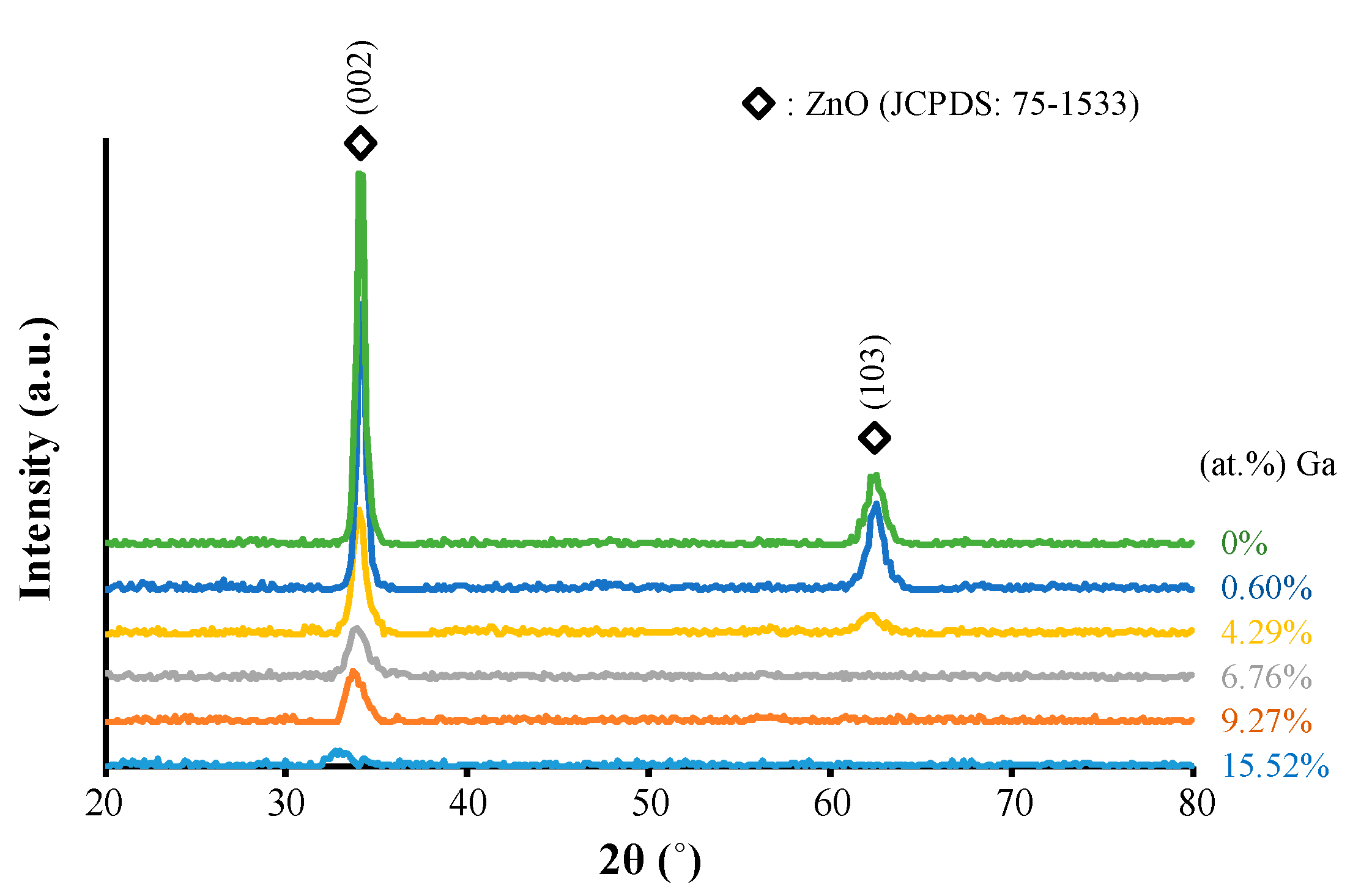
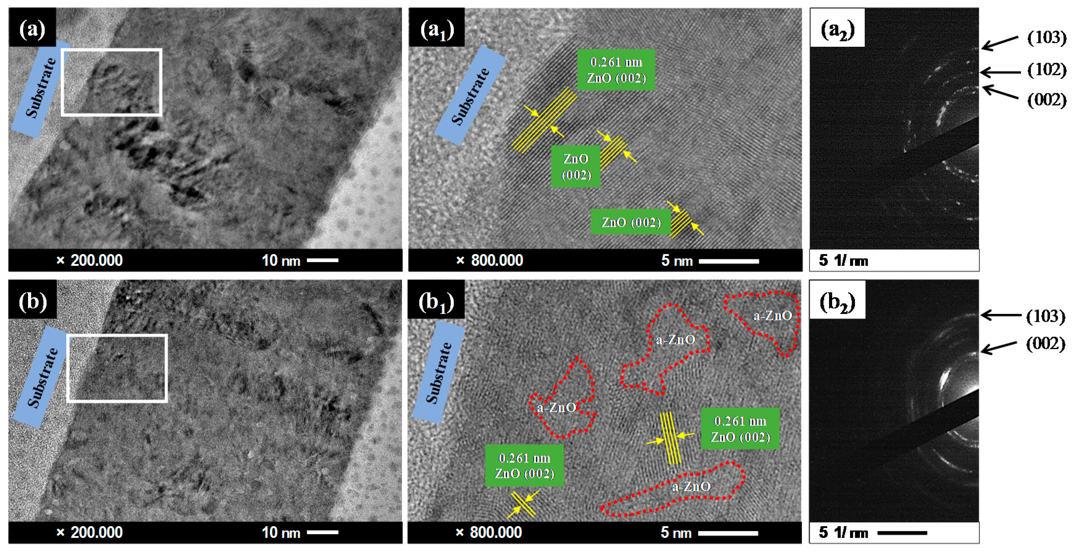
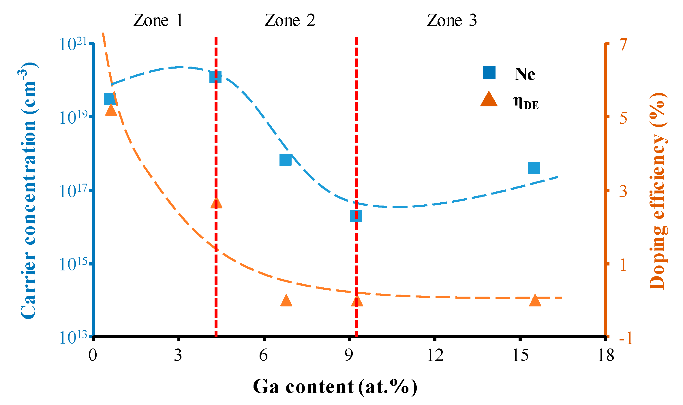
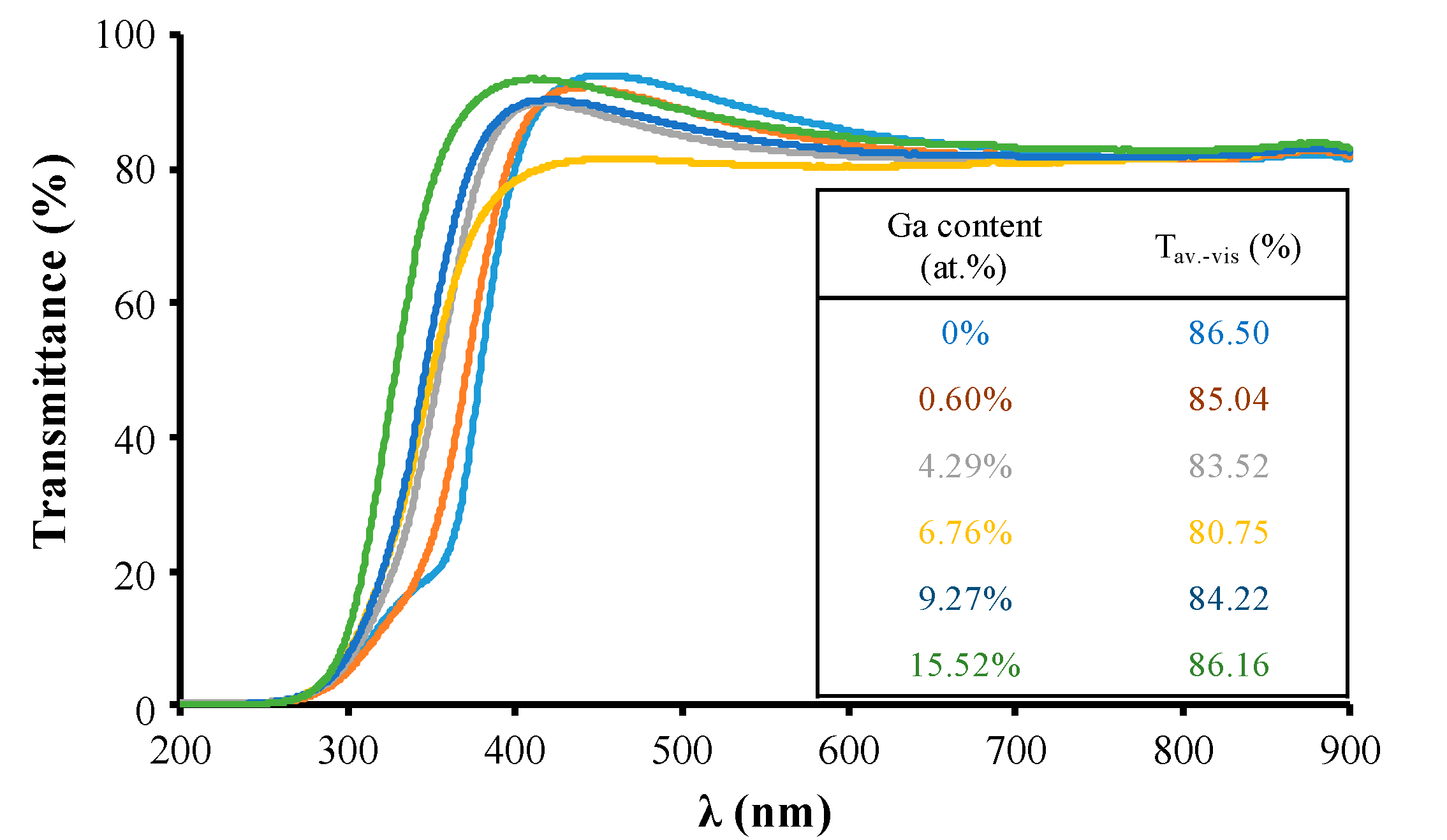
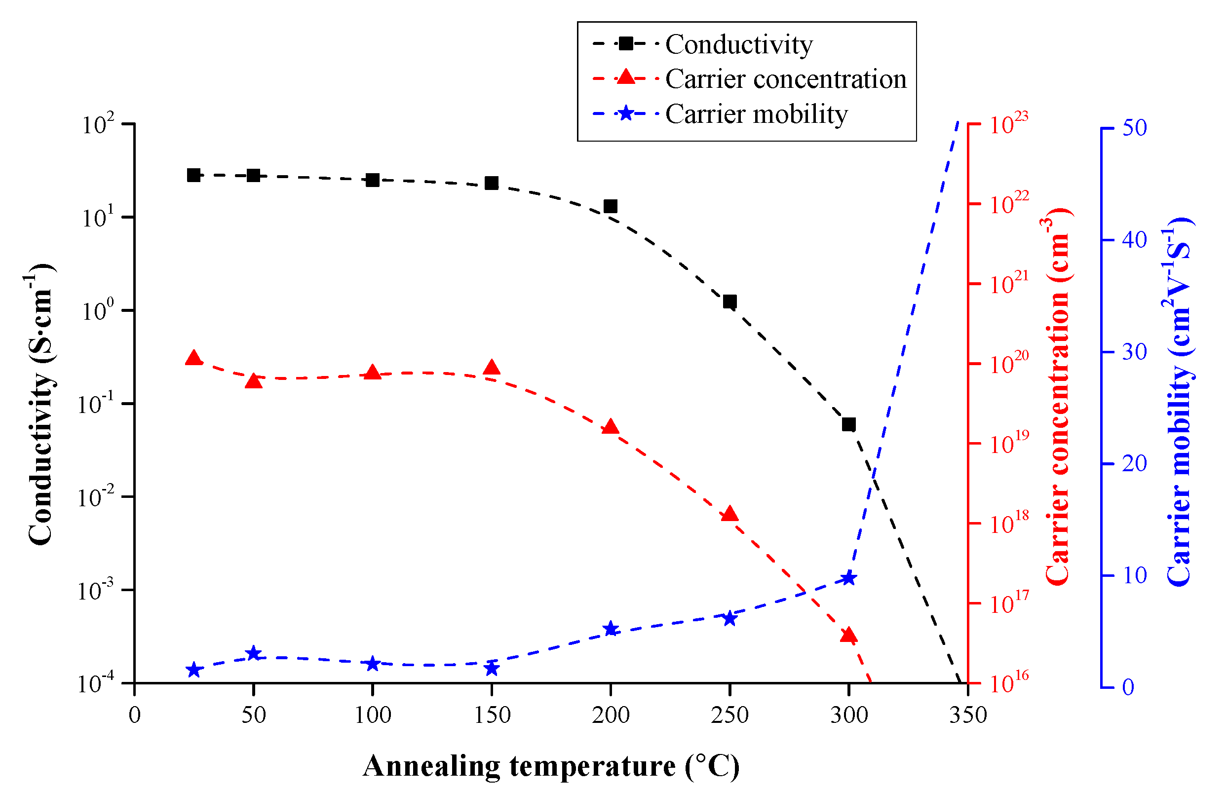
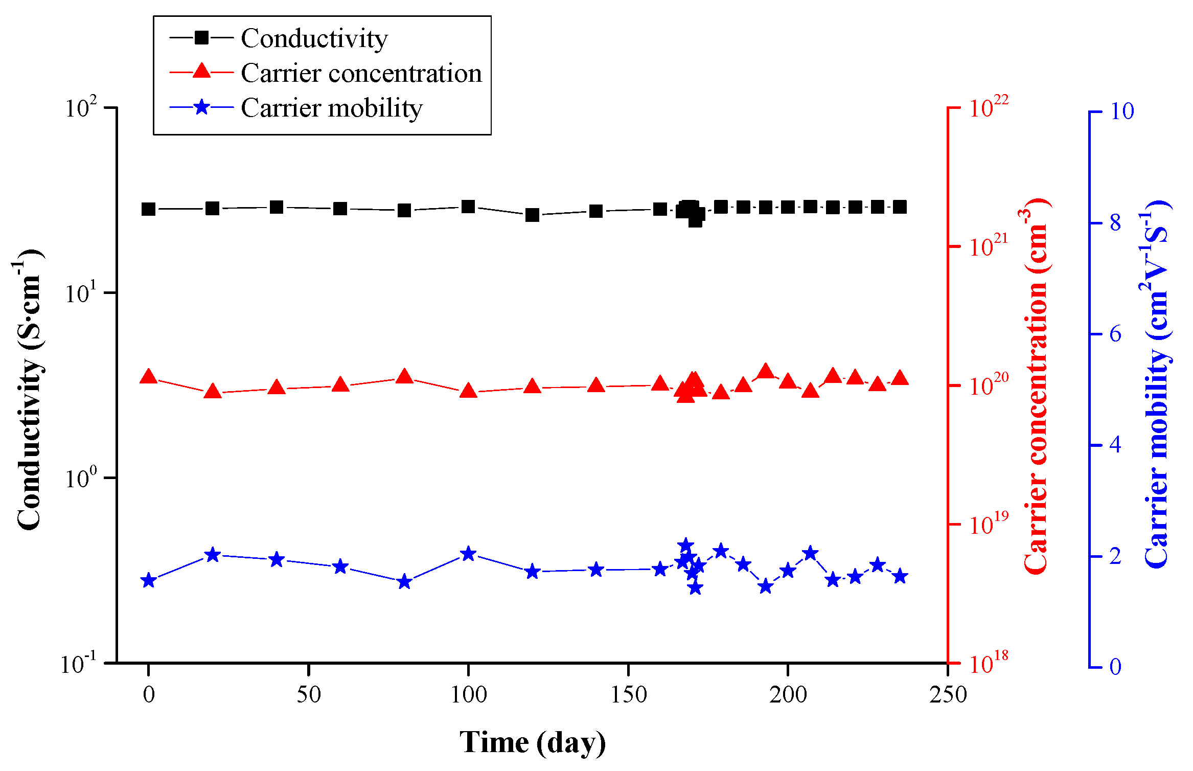
2. Results and Discussion

The influence of the sputtering power applied to the Ga2O3 target (PGa2O3) on the variation in Ga content in the films was first investigated. The results are shown in Figure 1. With increases in PGa2O3, Ga content initially increased slightly (PGa2O3 < 20 W) before rising significantly as PGa2O3 rose above 20 W. The actual Ga content of the films with various PGa2O3 is given in the inset table. ZnO with 0.60 at % Ga thin film was obtained when PGa2O3 was fixed at 20 W. When PGa2O3 was above 30 W, Ga content increased to more than 4.29 at %. As reported by H. Gomez [22] and R. Wang [23], the solubility limit of Ga in ZnO is around 2–3 at % at room temperature. If more Ga is introduced into ZnO thin film, the redundant gallium atoms will segregate from the ZnO lattice and form neutralized gallium species in the grain boundaries of ZnO.
The X-ray diffraction patterns of the ZnO thin films with varying amounts of Ga are shown in Figure 2. When the doping content of Ga was about 0.6 at %, no obvious peak shift was observed. Even though the ionic radius of Ga3+ (0.062 nm) is smaller than that of Zn2+ (0.074 nm) [24], the amount of Zn2+ cations replaced by Ga3+ cations was at a very low level, so the contraction in lattice parameters was not considerable. However, when the content of Ga3+ cations exceeded 4.29 at %, the ZnO diffraction peaks moved to lower diffraction angles. This movement became more pronounced with the rise in Ga content owing to redundant Ga atoms entering into the ZnO lattice and forming Ga interstitial (Gai) defects, which enlarged the lattice parameters of ZnO. Moreover, as the extrinsic defects of (GaZn) (the substitution of Zn by Ga), and (Gai) were introduced into the ZnO films, the films’ crystallinity degraded as the Ga content increased.
The degradation of the film’s crystallinity with increasing Ga content was revealed by TEM observation (Figure 3). The crystallinity of GZO films with more gallium (PGa2O3 = 50 W) was found to be inferior to those with less gallium (PGa2O3 = 30 W). Some amorphous domains (highlighted by red dotted lines) embedded in the crystallized ZnO are visible in Figure 3b1, but none can be found in Figure 3a1. Additionally, in comparing the selected area electron diffraction (SAED) patterns of these two films, the conversion of the diffraction spots (Figure 3a2) to the diffraction rings (Figure 3b2) indicated an obvious reduction in grain size, which degraded the film’s crystallinity.
The film’s conductivity as a function of Ga content in ZnO films is shown in Figure 4. The conductivity of the film without Ga doping was too low to be detected under our experimental conditions. After the Ga doping of ZnO, the film’s conductivity significantly improved when the doping concentration was less than 4.29 at %, a range (Zone 1) in which Zn2+ cations were effectively replaced by Ga3+ cations. However, this improvement of the film’s conductivity disappeared when the Ga3+ content increased to a range of 4.29–9.27 at % (Zone 2), due mainly to the Ga content exceeding its solubility in ZnO and neutralized gallium atoms separating from the ZnO lattice. These neutralized species could not contribute to the generation of free electrons and enhanced the scattering effect of the carriers in ZnO films. Therefore, the film’s conductivity declined in this range. Upon a further increase in Ga content to 15.52 at % (Zone 3), the film’s conductivity improved because the neutralized gallium atoms gathered together and formed Ga clusters due to the high Ga doping concentration. Given that the work functions of gallium and intrinsic ZnO are about 4.2 eV and 4.5 eV, respectively [25], ohmic contact occurred between the metallic gallium and n-type ZnO. As a result, the abundant electrons in gallium easily transferred into the ZnO, and the film’s conductivity thus increased.
The variation in the carrier concentration in the films with increasing Ga concentration was analyzed via Hall measurement, and the results are shown in Figure 5. The carrier concentration exhibited a trend similar to that of the film’s conductivity and revealed the formation and development of neutralized gallium species. When the Ga content was relatively low (Zone 1), most gallium atoms were ionized and replaced Zn2+ cations. Free electrons were derived from this replacement. Thus, the carrier concentration increased with rising gallium content. In Zone 2, the carrier concentration decreased due to an increasing number of gallium atoms separating from the ZnO lattice and forming neutral defects, which did not contribute to the generation of free electrons. Furthermore, the intrinsic donor defects of oxygen vacancies could be occupied by Ga atoms, which reduced the carrier concentration. In Zone 3, gallium atoms gathered into clusters, and more electrons could easily transfer from gallium clusters to ZnO films. Thus, the carrier concentration increased.
In order to understand the effective doping amount and the electrical activity of gallium in the ZnO films, the doping efficiency (ηDE) of Ga3+ cations in ZnO was also investigated (Figure 5). ηDE is defined as the ratio of the carrier concentration to the atomic ratio of Ga/(Ga + Zn), where the free electrons in ZnO films are mainly considered to be created by Ga substitution. As shown in Figure 5, the doping efficiency decreased with increasing gallium content, suggesting that more gallium atoms separated from the ZnO as gallium content increased.
The film’s transmittance is shown in Figure 6. Regardless of the Ga content of the ZnO, the films presented high transmittance in the visible region (400 nm to 800 nm). Their average transmittance was always above 80%. When the Ga content was increased from 0 at % to 6.76 at %, the number of defects, such as (GaZn) and (Gai), and Ga clusters increased, and the light scattering by these defects and clusters was enhanced. Hence, a slight decrease in the film’s transmittance was observed in this region. With further increases in Ga content, gallium clusters gathered together, increasing in size while decreasing in number. The film’s transmittance then improved. In addition, with increases in Ga content, blue shifting of the absorption edge was observed, corresponding to the expansion of the film’s band gap. According to Vagard’s law mentioned in [26], because the band gap of Ga2O3 is about 4.9 eV larger than that of ZnO, the band gap of Zn1-xGaxO films should increase linearly as the Ga doping amount increases.
The film’s electrical thermal stability is shown in Figure 7. A ZnO film with 4.29 at % Ga was annealed at various temperatures under normal atmospheric conditions. When the annealing temperature was below 200 °C, the film’s conductivity was slightly degraded with increasing annealing temperature because the oxygen vacancies (VO) in the ZnO film were occupied by oxygen in oxygenated conditions. As reported by A.F. Kohan [27], oxygen vacancies, as the most important intrinsic donor defect, are favorable to the film’s n-type conductivity. Therefore, with the reduction in the number of oxygen vacancies, the carrier concentration also decreased. In addition, due to the reduction in the number of VO defects, the carrier scattering by these defects was restricted, so the carrier mobility improved.
The melting point of gallium is only around 29.7 °C [28], and the partial pressure of indium atoms on the surface of the film is much lower than the saturated vapor pressure of indium. Therefore, when the annealing temperature exceeded 200 °C, the neutral gallium atoms that could not replace Zn cations obtained sufficient energy to migrate to the surface of the ZnO film, where they easily reacted with oxygen and formed insulating oxides. Hence, the carrier concentration and conductivity significantly dropped, and the carrier mobility increased. When the annealing temperature was higher than 300 °C, the film became completely insulating.
The film’s electrical time stability is given in Figure 8. The ZnO film with 4.29 at % Ga was placed in normal atmospheric conditions at ambient temperature for more than 240 days. With prolonged analysis time, the film’s electrical properties remained almost unchanged. In other words, the occupation of oxygen vacancies by oxygen atoms in oxygenated conditions could be activated only at high temperatures. Furthermore, gallium atoms cannot migrate in a ZnO lattice spontaneously at room temperature. Accordingly, the ZnO/Ga films presented satisfactory time stability.

3. Materials and Methods

3.1. Deposition Parameters

Ga-doped ZnO (GZO) thin films with a thickness of about 100 nm were deposited on Corning 1737F glass substrates at room temperature via rf sputtering. The substrate holder rotation rate was about 10 rpm. Pure Ar was used as the working gas, and the working pressure was about 0.67 Pa. The sputtering power applied to the ZnO target (purity 99.95%, diameter 2.54 cm) was fixed at 80 W, while the sputtering power applied to the Ga2O3 target (purity 99.95%, diameter 2.54 cm) varied from 0 to 80 W. The power densities applied on ZnO and Ga2O3 targets are given in Table 1 and Table 2. Other sputtering parameters maintained during the deposition of GZO thin films are shown in Table 3.

3.2. Materials Characterizations

The thickness of the films was measured with a surface profilometer (Surfcoder SE-2300, Kosaka Laboratory Ltd., Tokyo, Japan). The composition of the films was detected with an electron probe X-ray microanalyzer (EPMA, JXA-8900R, JOEL, Tokyo, Japan). The phase structures of the films were analyzed with an X-ray diffractometer (XRD, X’Pert PRO MRD, Philips PANalytical, Almelo, The Netherlands) using the thin film mode with an incidence angle of 1°. Hall effect analysis (AHM-800B, Agilent Technologies, Santa Clara, CA, USA) with van der Pauw’s configuration was employed to investigate the electrical properties of the films. Finally, the transmittance of the films was measured with a UV-Vis spectrophotometer (JASCO-V650, JASCO, Tokyo, Japan).

4. Conclusions

GZO films were deposited via rf sputtering. The optoelectronic properties of the films as a function of Ga content were investigated. It was found that, when the gallium content was near 4.29 at %, ZnO/Ga films possess optimal electrical properties. All such ZnO films present high transmittance in the visible region, regardless of gallium content. In addition, due to the occupation of oxygen vacancies by oxygen atoms and the migration of gallium atoms in ZnO film, the film’s electrical properties are degraded under high temperatures in oxygenated conditions. However, this degradation was not observed in the time stability examination. This result suggests that ZnO/Ga films can withstand long-term loads at ambient temperatures but are not suitable for applications in high-temperature environments.

Acknowledgments

We gratefully acknowledge the National Natural Science Foundation of China (No. 51172217) and Ministry of Science and Technology of Taiwan (No. 103-2221-E-131-004) for their financial support. We also thank H.C. Lin and C.Y. Kao of the Instrumentation Center, National Taiwan University, for EPMA experiments.

Author Contributions

Sheng-Chi Chen and Shien-Uang Jen conceived and designed the experiments; Jian-Yu Chen performed the experiments; Hui Sun and Xin Wang analyzed the data; Hai-Pang Chiang contributed reagents/materials/analysis tools; Hui Sun wrote the paper.

Conflicts of Interest

The authors declare no conflict of interest.

References

  1. Chen, X.L.; Liu, J.M.; Ni, J.; Zhao, Y.; Zhang, X.D. Wide-spectrum Mg and Ga co-doped ZnO TCO thin films for solar cellsgrown via magnetron sputtering with H2 introduction. Appl. Surf. Sci. 2015, 328, 193–197. [Google Scholar] [CrossRef]
  2. Kim, S.I.; Cho, S.H.; Choi, S.R.; Oh, M.C.; Jang, J.H.; Song, P.K. Crystallization and electrical properties of ITO: Ce thin films for flat panel display applications. Thin Solid Films 2009, 5107, 4061–4064. [Google Scholar] [CrossRef]
  3. Ko, Y.D.; kim, K.C.; Kim, Y.S. Effects of substrate temperature on the Ga-doped ZnO films as an anode material of organic light emitting diodes. Superlattices Microstruct. 2012, 51, 933–941. [Google Scholar] [CrossRef]
  4. Bartens, R.; Jelle, B.P.; Gustavsen, A. Properties, requirements and possibilities of smart windows for dynamic daylight and solar energy control in buildings: A state-of-the-art review. Sol. Energy Mater. Sol. Cells 2010, 94, 87–105. [Google Scholar] [CrossRef]
  5. Domaradzki, J. Perspectives of development of TCO and TOS thin films based on (Ti-Cu) oxide composites. Surf. Coat. Technol. 2016, 290, 28–33. [Google Scholar] [CrossRef]
  6. Sibin, K.P.; Swain, N.; Chowdhury, P.; Dey, A.; Sridhara, N.; Shashikala, H.D.; Sharma, A.K.; Barshilia, H.C. Optical and electrical properties of ITO thin films sputtered on flexible FEP substrate as passive thermal control system for space applications. Sol. Energy Mater. Sol. Cells 2016, 145, 314–322. [Google Scholar] [CrossRef]
  7. Yu, S.H.; Yang, W.H.; Li, L.X.; Zhang, W.F. Improved chemical stability of ITO transparent anodes with a SnO2 buffer layer for organic solar cells. Sol. Energy Mater. Sol. Cells 2016, 144, 652–656. [Google Scholar] [CrossRef]
  8. Li, Y.P.; Sun, J. The modification of electrical properties of Au/n-Hg3In2Te6 Schottky contact by the introduction of ITO interlayer. Curr. Appl. Phys. 2016, 16, 623–627. [Google Scholar] [CrossRef]
  9. Aleksandrova, M.; Kurtev, N.; Videkov, V.; Tzanova, S.; Schintke, S. Material alternative to ITO for transparent conductive electrode in flexible display and photovoltaic devices. Microelectron. Eng. 2015, 145, 112–116. [Google Scholar] [CrossRef]
  10. Linss, V. Comparison of the large-area reactive sputter processes of ZnO:Al and ITO using industrial size rotatable targets. Surf. Coat. Technol. 2016, 290, 43–57. [Google Scholar] [CrossRef]
  11. Tubtimtae, A.; Lee, M.W. ZnO nanorods on undoped and indium-doped ZnO thin films as a TCO layer on nonconductive glass for dye-sensitized solar cells. Superlattices Microstruct. 2012, 52, 987–996. [Google Scholar] [CrossRef]
  12. Chen, S.C.; Wang, C.H.; Sun, H.; Wen, C.K.; Lu, C.F.; Tsai, C.L.; Fu, Y.K.; Chuang, T.H. Microstructures, electrical and magnetic properties of (Ga, Co)-ZnO films by radio frequency magnetron co-sputtering. Surf. Coat. Technol. 2016, 303, 203–208. [Google Scholar] [CrossRef]
  13. Jayaraman, V.K.; Alvarez, A.M.; Kuwabara, Y.M.; Koudriavstev, Y.; Amador, M.O. Effect of co-doping concentration on structural, morphological, optical and electrical properties of aluminium and indium co-doped ZnO thin films deposited by ultrasonic spray pyrolysis. Mater. Sci. Semicond. Process. 2016, 47, 32–36. [Google Scholar] [CrossRef]
  14. Wang, F.H.; Chang, C.L. Effect of substrate temperature on transparent conducting Al and Fco-doped ZnO thin films prepared by rf magnetron sputtering. Appl. Surf. Sci. 2016, 370, 83–91. [Google Scholar] [CrossRef]
  15. Jin, C.; Narayan, R.; Tiwari, A.; Zhou, H.H.; Kvit, A.; Narayan, J. Epitaxial growth of zinc oxide thin films on silicon. Mater. Sci. Eng. B 2005, 117, 348–354. [Google Scholar] [CrossRef]
  16. Snure, M.; Tiwari, A. Structure, electrical, and optical characterizations of epitaxial films grown on sapphire (0001) substrate. J. Appl. Phys. 2007, 101, 124912. [Google Scholar] [CrossRef]
  17. Jang, C.; Jiang, Q.J.; Lu, J.G.; Ye, Z.Z. Structural, optical and electrical properties of Ga doped ZnO/Cu grid/Ga doped ZnO transparent electrodes. J. Mater. Sci. Technol. 2015, 31, 1108–1110. [Google Scholar] [CrossRef]
  18. Yamada, Y.; Kadowaki, K.; Kikuchi, H.; Funaki, S.; Kubo, S. Positional variation and annealing effect in magnetron sputtered Ga-doped ZnO films. Thin Solid Films 2016, 609, 25–29. [Google Scholar] [CrossRef]
  19. Kim, J.H.; Yer, I.H. Characterization of ZnO nanowires grown on Ga-doped ZnO transparent conductive thin films: Effect of deposition temperature of Ga-doped ZnO thin films. Ceram. Int. 2016, 42, 3304–3308. [Google Scholar] [CrossRef]
  20. Bhosle, V.; Tiwari, A.; Narayan, J. Electrical properties of transparent and conducting Ga doped ZnO. J. Appl. Phys. 2006, 100, 033713. [Google Scholar] [CrossRef]
  21. Bhosle, V.; Tiwari, A.; Narayan, J. Metallic conductivity and metal-semiconductor transition in Ga-doped ZnO. Appl. Phys. Lett. 2006, 88, 032106. [Google Scholar] [CrossRef]
  22. Gomez, H.; Olvera, M.L. Ga-doped ZnO thin films: Effect of deposition temperature, dopant concentration, and vacuum-thermal treatment on the electrical, optical, structural and morphological properties. Mater. Sci. Eng. B 2006, 134, 20–26. [Google Scholar] [CrossRef]
  23. Wang, R.P.; Sleight, A.W. High Conductivity in Gallium-Doped Zinc Oxide Powders. Chem. Mater. 1996, 8, 433–439. [Google Scholar] [CrossRef]
  24. Shannon, R.D. Revised effective ionic radii and systematic studies of interatomic distances in halides and chalcogenides. Acta Cryst. A 1976, 32, 751–767. [Google Scholar] [CrossRef]
  25. Sundaram, K.B.; Khan, A. Work function determination of zinc oxide films. J. Vac. Sci. Technol. A 1997, 15, 428–430. [Google Scholar] [CrossRef]
  26. Snure, M.; Tiwari, A. Band-gap engineering of Zn1-xGaxO nanopowders: Synthesis, structural and optical characterizations. J. Appl. Phys. 2008, 104, 073707. [Google Scholar] [CrossRef]
  27. Kohan, A.F.; Ceder, G.; Morgan, D.; van de Walle, C.G. First-principles study of native point defects in ZnO. Phys. Rev. B 2000, 61, 15019–15027. [Google Scholar] [CrossRef]
  28. Dadzis, K.; Lukin, G.; Meier, D.; Bonisch, P.; Sylla, L.; Patzold, O. Directional melting and solidification of gallium in a traveling magnetic field as a model experiment for silicon processes. J. Cryst. Growth 2016, 445, 90–100. [Google Scholar] [CrossRef]
Figure 1. Ga content in ZnO thin films as a function of the sputtering power applied on the Ga2O3 target.
Materials 09 00987 g001
Figure 2. X-ray diffraction (XRD) patterns of ZnO thin films with varying amounts of Ga.
Materials 09 00987 g002
Figure 3. TEM observation and the corresponding high-resolution TEM images of Ga-doped ZnO (GZO) films deposited with Ga2O3 powers of 30 W (a,a1) and 50 W (b,b1), and their electron diffraction patterns: 30 W (a2) and 50 W (b2).
Materials 09 00987 g003
Figure 4. The variation in film conductivity as a function of Ga content in ZnO films.
Materials 09 00987 g004
Figure 5. The variation in carrier concentration Ne and doping efficiency ηDE as a function of Ga content (the bulk ZnO density of 5.606 g/cm3 was used to estimate ηDE).
Materials 09 00987 g005
Figure 6. The variation in film transmittance as a function of Ga content in ZnO films.
Materials 09 00987 g006
Figure 7. The electrical thermal stability of the ZnO film with 4.29 at % Ga under normal atmospheric conditions.
Materials 09 00987 g007
Figure 8. The electrical time stability of the ZnO film with 4.29 at % Ga at ambient temperature.
Materials 09 00987 g008
Table 1. The power densities applied on ZnO target.
Power (W)Power Density (W/cm2)
803.95
Table 2. The power densities applied on Ga2O3 target.
Power (W)Power Density (W/cm2)
00
200.99
301.48
401.97
502.47
803.95
Table 3. Sputtering parameters maintained during the deposition of GZO thin films.
ParameterValues
Background pressure (Pa)<6.7 × 10⁻⁴
Working pressure (Pa)0.67
Films thickness (nm)100
Rotation speed (rpm)10
SubstrateGlass/Silicon
Power (W)ZnO80
Ga2O30–80

