Article

Computational Search for Two-Dimensional MX2 Semiconductors with Possible High Electron Mobility at Room Temperature

State Key Laboratory of Electronic Thin Films and Integrated Devices, University of Electronic Science and Technology of China, Chengdu 610054, China
*
Author to whom correspondence should be addressed.
Materials 2016, 9(9), 716; https://doi.org/10.3390/ma9090716
Submission received: 18 July 2016 / Revised: 13 August 2016 / Accepted: 18 August 2016 / Published: 23 August 2016

Abstract

:
Neither of the two typical two-dimensional materials, graphene and single layer MoS 2 , are good enough for developing semiconductor logical devices. We calculated the electron mobility of 14 two-dimensional semiconductors with composition of MX 2 , where M (=Mo, W, Sn, Hf, Zr and Pt) are transition metals, and Xs are S, Se and Te. We approximated the electron phonon scattering matrix by deformation potentials, within which long wave longitudinal acoustical and optical phonon scatterings were included. Piezoelectric scattering in the compounds without inversion symmetry is also taken into account. We found that out of the 14 compounds, WS 2 , PtS 2 and PtSe 2 are promising for logical devices regarding the possible high electron mobility and finite band gap. Especially, the phonon limited electron mobility in PtSe 2 reaches about 4000 cm 2 ·V - 1 ·s - 1 at room temperature, which is the highest among the compounds with an indirect bandgap of about 1.25 eV under the local density approximation. Our results can be the first guide for experiments to synthesize better two-dimensional materials for future semiconductor devices.

1. Introduction

Two-dimensional (2D) layered materials have received a lot of research attention since the discovery of graphene. New materials such as transitional metal dichalcogenides (TMDs), especially MoS 2 [1], and black phosphorus [2], with one or several atomic layers, were synthesized. Field effect transistors (FET) [3], phototransistors [4] and light harvest devices [5] were fabricated to demonstrate the potential applications of these new materials. The reduced thickness is promising for improving transistor performances and adding new applications in the coming decades [6]. Very recent reviews of the electronic properties of these 2D materials and their applications can be found in Ref. [7,8] and references therein. As mentioned there, the carrier mobility is one of the key parameters for semiconductors to be used in high speed or high frequency devices. Therefore, high speed radio frequency devices, which make full use of the ultrahigh electron mobility in graphene [8], were fabricated. However, due to the intrinsic zero bandgap, the on/off ratio was small (<10 5 ) when it was used in logical devices. In order to be good candidates in logical devices, the materials are required to have both a sizable bandgap and a high carrier mobility. Monolayer MoS 2 has a direct band gap of about 1.7 eV. However, the electron mobility [9] at room temperature is less than 100 cm 2 ·V - 1 ·s - 1 without other techniques such as dielectric gating and ion gating [10], where the later techniques can increase the mobility up to 200 cm 2 ·V - 1 ·s - 1 . Some more MX 2 monolayers have been fabricated, especially WS 2 , WSe 2 , and MoSe 2 , where the highest electron mobility reaches 142 cm 2 ·V - 1 ·s - 1 in WSe 2 [11]. Black phosphorus shows a bandgap tunable from 1.51 eV for a monolayer to 0.59 eV for a five-layer sample [12] with the thickness-dependent charge-carrier mobility with the highest values up to ∼1000 cm 2 ·V - 1 ·s - 1 obtained for a thickness of ∼10 nm [13].
A natural question arises of whether we can find 2D TMDs with larger carrier mobilities or not. This question can be answered by theoretical calculations. The upper bound of the mobility is set by the unavoidable intrinsic scatterings. For example, phonon scattering is the one that cannot be avoided at temperatures other than zero and is the main source of scattering at room temperature. There are quite a few works to calculate the phonon-limited carrier mobility in 2D materials, which was started by Kaasbjerg et al. [14,15], where a supper-cell method was used. The electron–phonon, as well as the piezoelectric interactions, were taken into account. The calculated electron mobility at room temperature is about 410 cm 2 ·V - 1 ·s - 1 . This parameter estimated by Restrepo et al. [16] is 225 cm 2 ·V - 1 ·s - 1 . Li et al. [17] developed the method to calculate the electron–phonon interactions based on the density functional perturbation theory and obtained similar results to Kaasbjerg. They extend their calculations to electron and hole mobilities of four monolayer transition metal dichalcogenides [18]: MoS 2 , MoSe 2 , WS 2 and WSe 2 . WS 2 has the highest electron and hole mobilities. It was also predicted that p-type WSe 2 shows hole mobilities comparable or even larger than that of bulk silicon at the room temperature.
Our previous work shows that MoTe 2 , ZrSe 2 and HfSe 2 have the largest electron mobility if only long wave acoustical phonon scattering was taken into account [19]. However, as shown in the work of Kaasbjerg [14], the optical phonon may also play an equally important role in MoS 2 in the room-temperature due to the small optical phonon energy. In this work, we take these effects into account and try to figure out MX 2 type 2D monolayer semiconductors with possible high electron mobilities. Because a direct calculation of electron–phonon scattering matrix is time and memory demanding, we approximate it by calculating the corresponding deformation potentials, where only several self-consistent electronic structure calculations are required. All the needed parameters can be extracted and can be done automatically. Thus, high-throughput calculations can be conducted that enables us to screen out the promising materials within a reasonable time. We found that out of the 14 compounds from the The Inorganic Crystal Structure Database (ICSC) database [20], only PtS 2 and PtSe 2 with the 1T-structure can have electron mobility larger than 3500 cm 2 ·V - 1 ·s - 1 . WS 2 has the electron mobility of about 1739 cm 2 ·V - 1 ·s - 1 , which is comparable with that of Si at room temperature.

2. Methods

Out of the ICSD database, only 16 compounds with MX 2 are semiconductors [20]. There are more layered compounds with more chemical elements. The complexity may hinder their practical applications. We selected 14 MX 2 compounds that crystallize into two different hexagonal crystal structures. One is the same as that of MoS 2 and the other is CdI 2 . They are also called 1H and 1T structure, respectively. The difference is that the anion hexagonal nets are A-A stacked in MoS 2 , while they are A-B stacked in CdI 2 as shown in Figure 1a,b, respectively. Thus, the first one has a mirror plane of the metals and lacks inversion symmetry, while the second one has the inversion center.
The calculations were performed mainly with pseudo-potential code PWscf [21], and crosschecked by the full-potential local-orbital code (FPLO) [22] in its current version with the default basis settings. All calculations were done within the scalar relativistic approximation. The local density approximation (LDA) functional was chosen to be that parameterized by Perdew and Wang [23]. The plane-wave kinetic energy cutoff was set to 90 Ry with density cut-off of 900 Ry. A shifted 17 × 17 × 2 Monkhorst–Pack mesh was used to perform Brillouin zone integration in order to ensure the convergence of the results. Convergence of the total energy was set to be better than 10 - 8 Hartree. A vacuum layer with thickness of 30 a.u. was used to model the 2D-nature of the compounds. Forces on the atoms are limited within 0.001 Ry/a B after full geometry relaxation. Phonon frequencies and phonon eigenvectors of at the Γ-point were calculated in a 4 × 4 × 1 q-grid under the density functional perturbation theory (DFPT). The electron mobilities (μ) were calculated by summation of the contributions of different scattering sources:
1 μ = 1 μ L A + 1 μ O P + 1 μ P Z ,
where μ L A is the longitudinal acoustic phonon determined mobility, μ O P is the longitudinal optical phonon and μ P Z is the piezoelectricity determined, respectively.

3. Results and Discussion

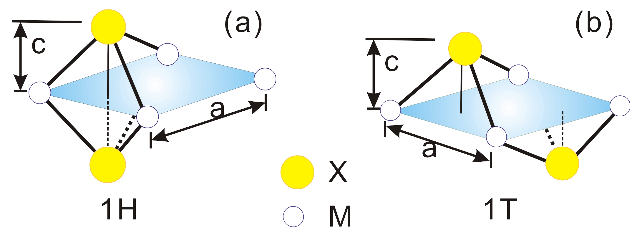
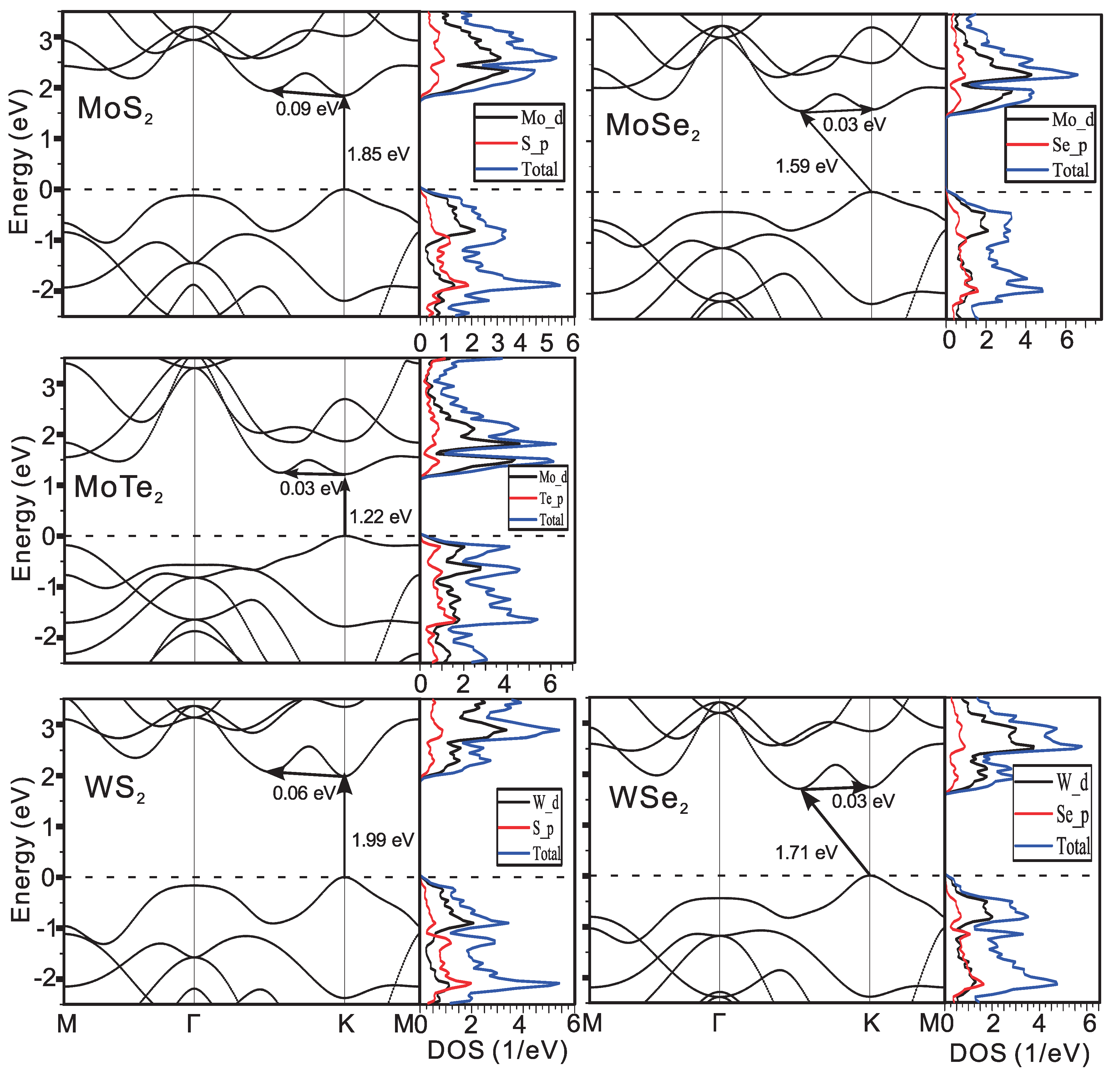
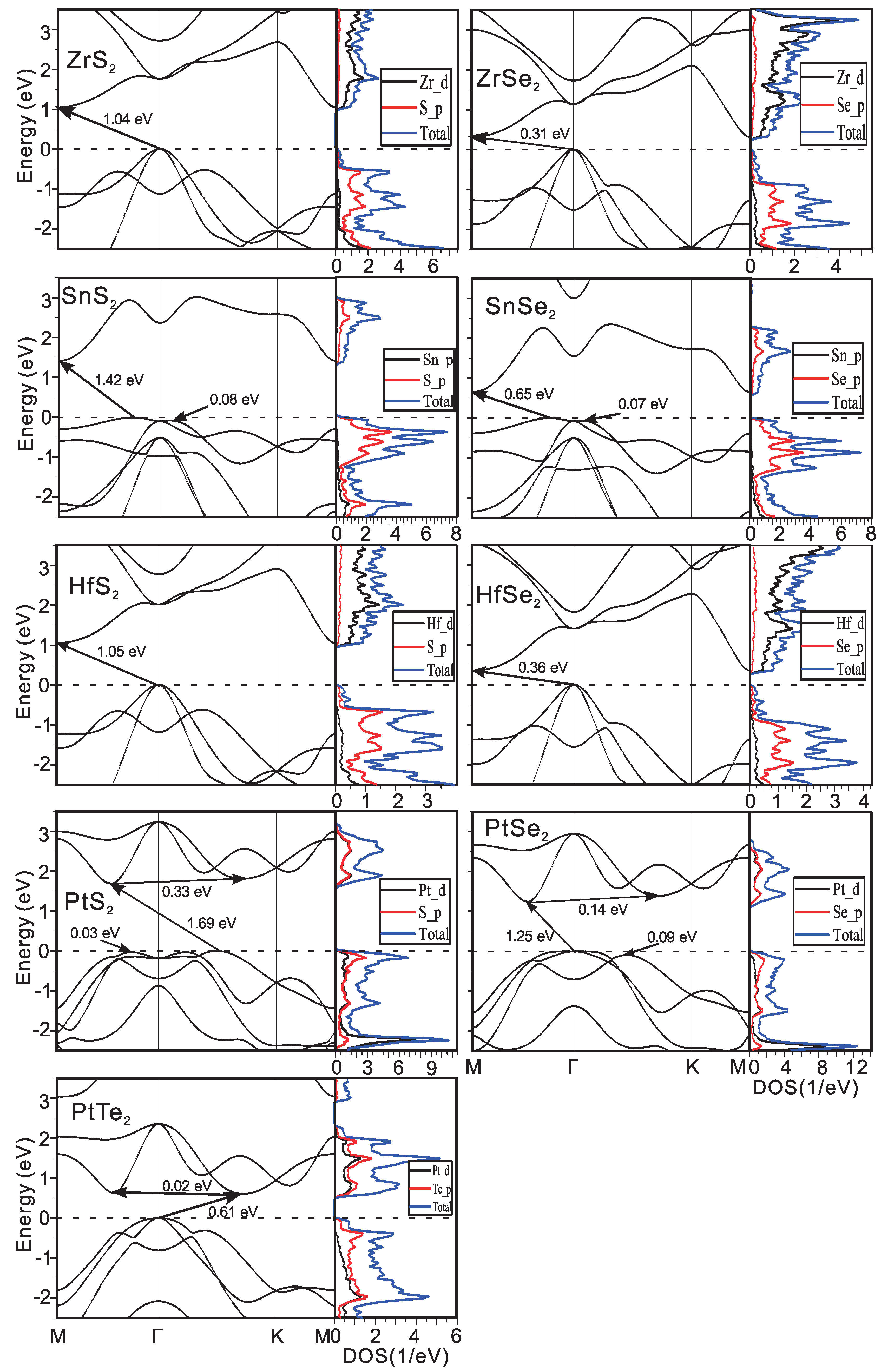
3.1. Electron and Phonon Dispersions

The electronic structures have been discussed in our previous work [19], where the most important parameters for the mobility are the effective masses of electrons. As seen in the previous works, the compounds with the 1T-structure are mostly anisotropic, while the ones with 1H-structures are more or less isotropic, which is obvious from the electronic bands in Figure 2 and Figure 3. The effective electron masses (m * ) and the bandgap by the local density approximation (LDA) are listed in Table 1. The m * of MoX 2 are about 0.5 (m e ), where (m e ) is the static mass of the free electron. The electron is even lighter in WX 2 , which is only about 0.25 m e . This will give systematically higher electron mobility. For the same metal atoms, with the increase of atomic number of X, the (m e ) slightly increases.
There is a sizable bandgap in all of these compounds ranging from 0.31 eV in ZrSe 2 to 1.99 eV in WS 2 by LDA. This value is usually systematically underestimated by LDA as we know. The electronic band structure and the atomic projected Density of States (pDOSs) of all these compounds are calculated as shown in Figure 2 and Figure 3 for the two structures. In the 1T-compounds, the conduction band minimum is located at the M-point except PtS 2 and PtSe 2 , where it lies between Γ - M in PtTe 2 . There is another local conduction band minimum (Q-valley) only tens of meV higher than the global conduction band minimum in the compounds, which gives additional electron scattering channels and reduces the electron mobility. The extra local minimum is also observed in compounds with 1H-structure. The DOS is projected onto different atomic orbitals as shown in the right side of the figures, which clearly show that the transition metal and the X-atoms both contribute to the states of the conduction bands in the 1H compounds. In 1T-structure, the situation is more complicated: in PtX 2 , the Pt and X-atoms contribute equally to the states. However, in HfX 2 and ZrX 2 , the contributions from the X-atoms are tiny and it is mainly due to the metal atoms, while these contributions are reversed in SnX 2 .
The phonon dispersions of the 1H and 1T structures are shown in Figure 4 and Figure 5. The characteristic homopolar phonon of the two-dimensional monolayer compounds are highlighted in the figure with red dashed lines. Within the compounds with the same metal atom, the frequency of the phonon increases with the atomic number. This is the consequence of the decrease of the chemical bond strength, where the forces between the atoms decrease and the atomic weight increases.
As the row number of X increases, the atoms become heavier and the bonds become less ionic. Changes of phonon energy are systematic. Taking PtX 2 as an example, the width of the acoustical branches decrease from 200 cm - 1 to 120 cm - 1 . The highest optical phonon frequency decreases from 380 cm - 1 to 180 cm - 1 . The gap between the optical and the acoustic branches also decreases with the decrease of the atomic weight differences. Especially, there is a gap about 100 cm - 1 between the optical and acoustic branches in PtS 2 . However, it diminishes in the other compounds with 1T-structure. The gaps also diminish in HfSe 2 and ZrX 2 . The larger phonon bandgap is favored to produce larger thermal conductivity due to the reduced acoustical and optical phonon inter-scattering. As calculated by Gu et al. [24], the thermal conductivity of 1H-type MX 2 are above 50 W/mK at room temperature, while those values of the 1T-type are much lower. The flat homopolar branch is quite obvious, as it is a characteristic of these layered structure compounds. The linear dispersion of the transversal acoustical (TA) branches becomes parabolic as the atomic number increases in PtX 2 due to the rapid decay of the transverse force constants.
Since the frequency of the optical phonon mode in these compounds is about tens of meV, which is comparable with the thermal energy of 30 meV at T = 300 K, it can have large populations at room temperature. Thus, both the acoustic and optical phonons may have the same order of contribution to the scattering processes.

3.2. Acoustic Phonon Scattering

The electron mobility limited by the LA phonon is approximated [25,26] by
μ L A = e 3 ρ V s 2 k B T m * m d E e l - p h 2 ,
where k B and are the Boltzmann constant and the Planck constant, respectively. m * is the effective mass of an electron in the electron propagation direction and m d is the electron density of state mass, which is m m , where m ( ) is the mass parallel (perpendicular) to the propagation direction. ρ is the mass density of the material. V s is the sound velocity in the corresponding direction, which is calculated by the supercell method, where a frozen phonon mode corresponding to the longitudinal phonon with vector q = π 8 a ( 1 , 0 , 0 ) was simulated. The phonon frequency ( ω k ) was obtained under the harmonic approximation, which is related to the sound velocity by ω k = V s | q | . The validity of this model has already been demonstrated. Bruzzone and Fiori used this model to compute the electron mobility of hydrogenated and fluorinated graphene as well as h-BCN from first principles. The results show that graphene with a reduced degree of hydrogenation can compete with silicon technology [27]. The electron phonon coupling (E e l - p h ) was approximated by the deformation potential D a c , which is related to the variation of the electron eigenvalue caused by the volume changes as
Δ E k = D a c Δ V V .
The related values are listed in Table 2, together with the values calculated from fitting the relaxation time obtained by Kim [18] and Kaasbjerg [14]. The values of MoS 2 obtained by Kaasbjerg is 2.4 eV, compared with 4.5 eV by Kim and our value of 3.9 eV lies between. The relative deviation of our values to the larger one of Kim is within 17 %, which will give lower electron mobility.

3.3. Optical Phonon Scattering

The zeroth order optical deformation potential D o p is defined as
Δ E = D o p d ,
where Δ E is the band energy shift under the corresponding deformation determined by the proper optical phonon mode. d is the atom displacement of the corresponding mode. There are six optical modes as shown in Figure 6, corresponding to six deformation potentials of the conduction band minimum.
The largest optical deformation potentials are listed in Table 2. The largest deformation potential was caused by the A 1 g (homopolar) mode of the phonon where the X atom moves in the opposite direction. The only exceptions are PtS 2 and PtSe 2 where the contributions are from the E mode. As reported in previous studies [28], the A 1 g mode is sensitive to electron doping and a red shift is observed on doping, which will increase the scattering rate. Thus, we can expect a significant decrease of the mobility. However, the in-plane mode is less sensitive to doping and the high mobility is expected to be kept.
The optical phonon limited mobilities are calculated by Equation (5) according to the relaxation time approximation:
μ O P = 2 e 2 ρ ω ν g d m d m * D o p 2 [ N ν Δ 1 + ( N ν + 1 ) Δ 2 ] ,
where g d is the valley degeneracy for the final electron states, N ν is the occupation number of phonon with angular frequency ω ν of mode ν, which is governed by Bose–Einstein distribution, and Δ 1 , 2 are the onsets of scattering for phonon absorption and emission, both of which are set to 1 for intravalley optical phonon scattering.

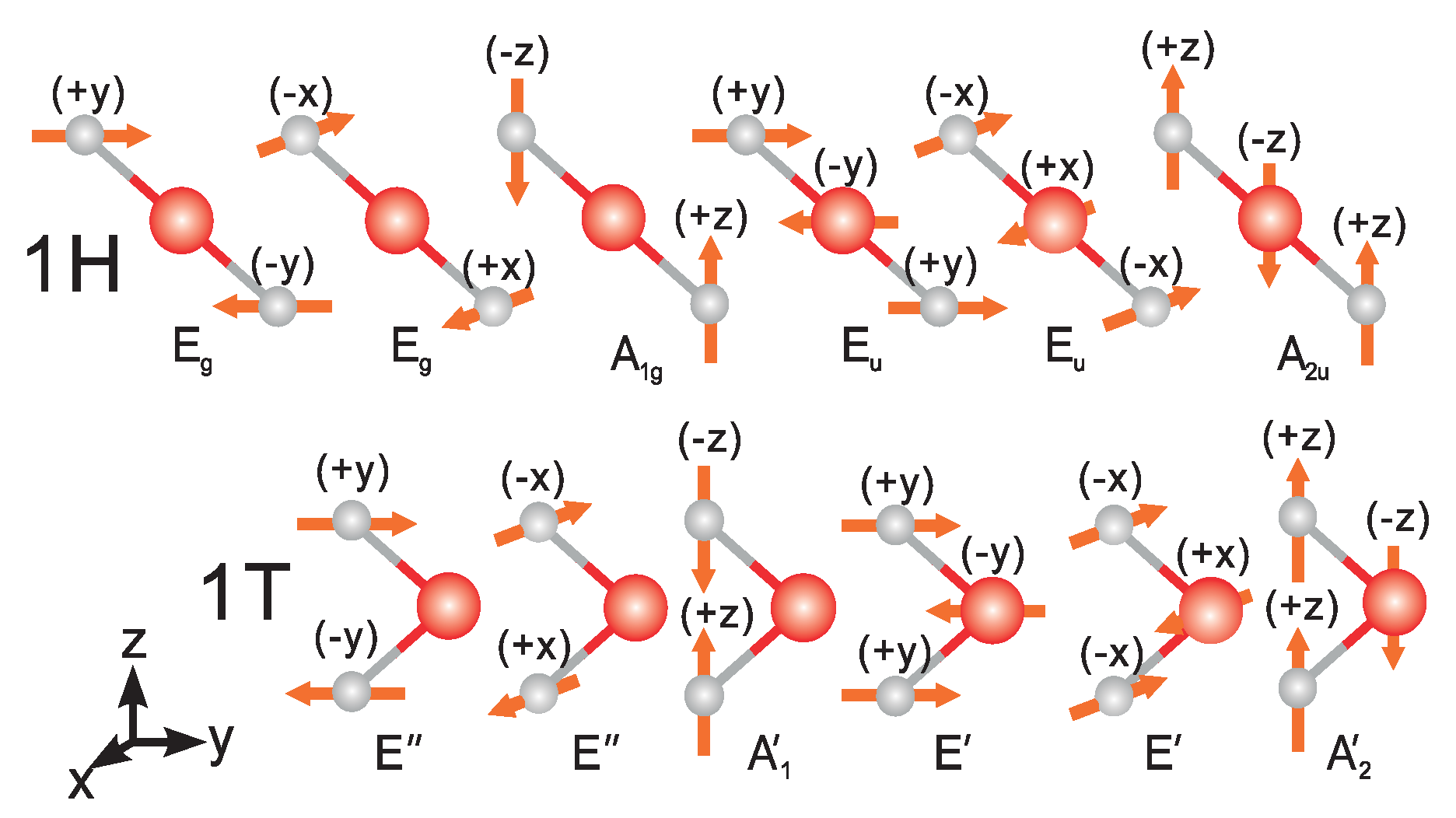
3.4. Piezoelectric Effects

When the inversion center is missed in the polar semiconductors, optical phonon deformation leads to electric polarization, which will be a scattering source of carriers. The piezoelectricity (PZ) induced scattering can be modeled in a similar way as the acoustic phonon scattering, where the PZ deformation potential D p z 2 = 1 2 ( e 11 e ϵ r ϵ 0 ) 2 substitutes E e l - p h 2 in Equation (2) to obtain the mobility [15]. The piezoelectric coefficient e 11 is defined in 2D materials, as linear response indicates that the piezoelectric effect could be treated as the first-order coupling between surface polarization and strain tensors ( ϵ i j ). The relation at fixed electric field E and temperature T is given by:
e i j k = ( P i ε j k ) E , T .
The symmetry requires that they are related by e 111 = e 11 , e 122 = e 12 = - e 11 , e 212 = e 221 = e 26 = - e 11 With the above relations, the piezoelectric coefficient is calculated by
P 1 ( ε 11 , ε 22 = 0 ) - P 1 ( ε 11 = 0 , ε 22 = 0 ) = e 11 ε 11 ,
where P is the polarization. In our calculation, the strains, ranging from −0.006 with steps of 0.002 to 0.006, are applied to the compounds. The calculated e 11 ’s are listed in Table 3 with comparison to the previous work [29].
It can be seen that the agreement is good, although our LDA values are systematically smaller than the GGA values reported by the work of Duerloo [29]. The e 11 s of the MoX 2 compounds are larger than the WX 2 compounds and decrease with the increase of the atomic number of X (X = S, Se, Te). The values are in the same order of bulk piezoelectric materials, which makes significant contributions to the scattering of the electrons. However, this scattering can be screened by dielectric medium as shown in experiments, which may explain the enhanced carrier mobilities by the proper choice of dielectric surroundings.

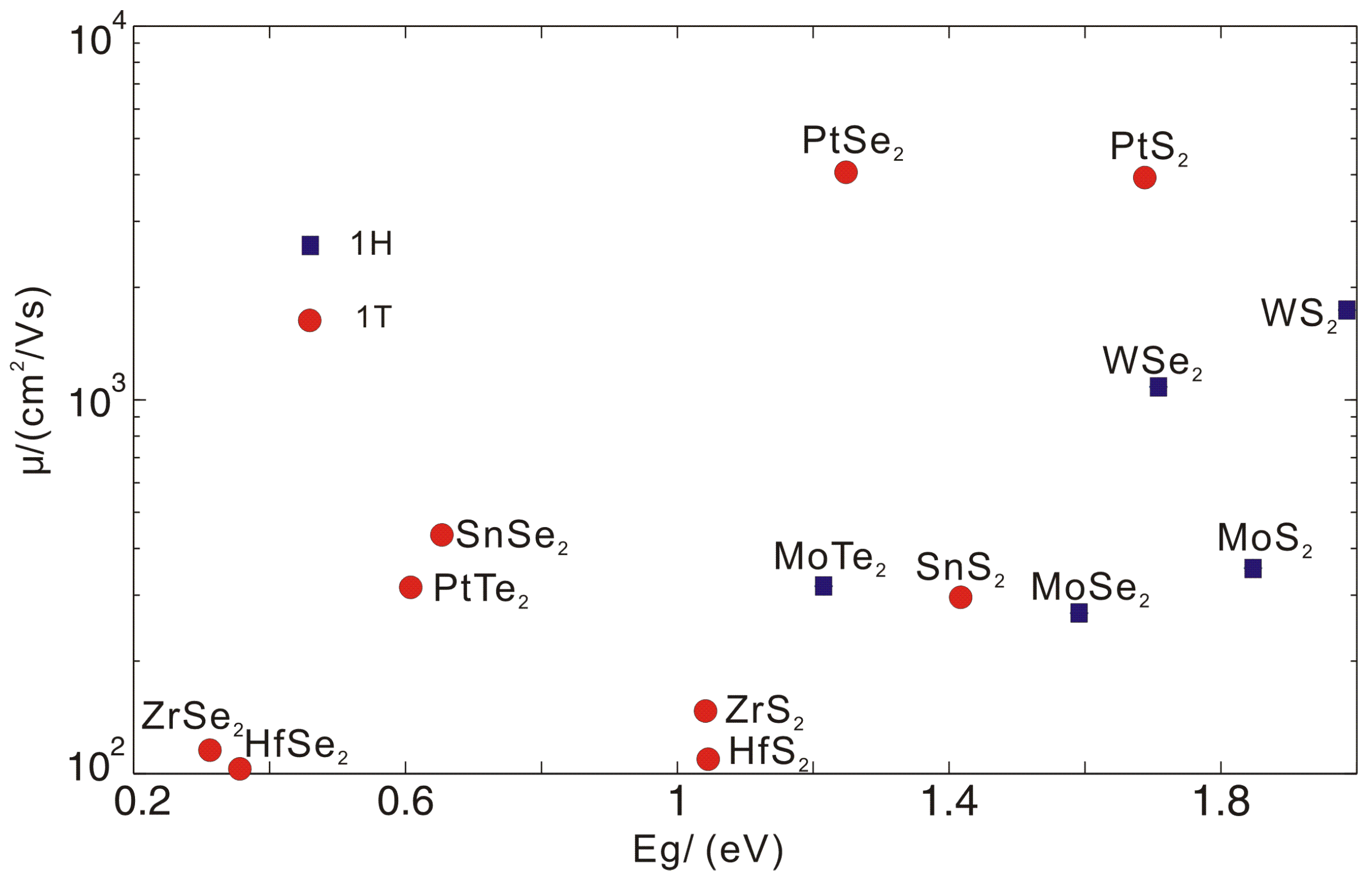
3.5. The Total Mobilities

The total electron mobilities were calculated by Matthiessen’s [30] rule as shown in Equation (1), where the contributions from the longitudinal acoustic, the optical phonons and the piezoelectric scattering were included when necessary. The data are listed in Table 4 and also shown in Figure 7 with the bandgap from LDA. There are calculations of the bandgap with PBE [31,32] and more expensive G 0 W 0 [32,33]. Our LDA gaps lie between the PBE and G 0 W 0 ones in the compounds with the 1H-structure, while it is the smallest among the three schemes in the compounds with 1T-structure. However, when compared with the experiments, there will be no obvious better agreements achieved when the G 0 W 0 is used. At the same time, the G 0 W 0 calculations give band structure as an almost rigid shift of the LDA or GGA ones, which will not change our main results of the electron mobilities here. It can also be seen from Table 4 that the optical phonon scattering largely reduces the electron mobility, which is the main source of scattering. For example, we can see that HfSe 2 and ZrSe 2 show larger acoustic phonon limited mobilities, but the optical phonon scattering is strong, which reduces the electron mobility to be less than 120 cm 2 ·V - 1 ·s - 1 . The total mobility and the LDA band gap are shown in Figure 7.
Among the compounds with the 1H structure, WS 2 and WSe 2 have mobilities of 1739 and 1083 cm 2 ·V - 1 ·s - 1 , respectively, which is nearly the same of Si (∼1750 cm 2 ·V - 1 ·s - 1 ). When compared with the up-to-date experimental data, there is quite a lot of room to increase the electron mobility. The well-studied MoS 2 has the upper limit of 354 cm 2 ·V - 1 ·s - 1 according to our calculation. The experimental value achieved now is about 200 cm 2 ·V - 1 ·s - 1 , which is already quite near this theoretical upper limit. The electron mobilities of MoX 2 compounds are low, which is mainly limited by the optical phonon scattering. This is in agreement with the previous calculations and analyses by Kaasbjerg et al. According to our calculations, the mobility of WSe 2 and WS 2 may be larger than MoS 2 . The mobility magnitude order is WS 2 > WSe 2 > MoS 2 > MoSe 2 , which is the same as the results by Kim et al. [18]. where the electron–phonon scattering matrix is computed. However, in the WS(Se) 2 compounds, the experimental values are only about tens of cm 2 ·V - 1 ·s - 1 , which is far below our theoretical limit. Recently, mobilities of WSe 2 and MoS 2 are extracted from the transfer character curves of field-effect transistors [34]. It is shown that the electron mobility in WSe 2 is about 110 cm 2 ·V - 1 ·s - 1 , while that of MoS 2 is about 25 cm 2 ·V - 1 ·s - 1 . These experimental results can be a preliminary confirmation of our prediction.
In the compounds with 1T-structures, the piezoelectric scattering is absent due to the presence of the inversion symmetry. However, the electron mobility is very limited by the optical scattering. Only two compounds, PtS 2 and PtSe 2 , show the high electron mobilities of 3942 and 4038 cm 2 ·V - 1 ·s - 1 with the LDA band gaps of 1.69 and 1.25 eV, respectively. These compounds are thus promising for semiconductor logical devices when compared with those parameters with Si.
In this work, we have considered only the long wave longitudinal acoustic and optical phonon scattering. The initial and final states of the scattered electrons are limited to the bottom of the conduction band. That is to say, only the intravalley scattering is included. There are other scattering processes, such as interband scattering, and other scattering sources like impurities, electrons and so on. The mobility will be limited by any one of these mechanisms. Thus, by computing the dominant scattering sources, the upper bound of the mobility can be estimated. We thus can say that it is hopeful that we can find compounds with possible high mobility among the selected ones with larger upper bounds. It is NOT possible to find larger mobility in the compounds that are predicted to have lower theoretical upper bounds. More sophisticated calculations are needed to aim more precisely within the reduced number of compounds.

4. Conclusions

To summarize, the electron mobility of 14 MX 2 type two-dimensional semiconductors were calculated where the elastic scattering from the long wave acoustic and optical phonons were taken into account by the deformation potential approximation. The piezoelectric scattering was also included in compounds without the inversion center and treated as the acoustic phonon-like deformation potential. We found that the total electron mobility in WS 2 can reach 1739 cm 2 ·V - 1 ·s - 1 , which is the highest value among the compounds with the 1H-structures. The values of 4038 cm 2 ·V - 1 ·s - 1 and 3942 cm 2 ·V - 1 ·s - 1 can be reached in PtSe 2 and PtS 2 with the 1T-structure, where the inversion center is presented and the piezoelectric scattering is prohibited. WS 2 is a direct band gap semiconductor with the bandgap of 1.99 eV at the K-point, while PtS 2 and PtSe 2 have the indirect bandgaps of 1.69 eV and 1.25 eV according to our LDA calculations. Concerning these two requirements of bandgap and electron mobility, these three compounds are promising for two-dimensional semiconductors used in future logical devices.

Acknowledgments

Financial support from the "863”-project (2015AA034202), a Research Grant from Chinese Central Universities (ZYGX2013Z001) and the National Natural Science Foundation of China (No. 2011JTD0006) are acknowledged.

Author Contributions

W.X.Z. proposed the calculation; Z.S.H. performed the calculations and W.L.Z supervised the calculations; Z.S.H. and W.X.Z. analyzed the data; Z.S.H. and W.X.Z. wrote the paper.

Conflicts of Interest

The authors declare no conflicts of interests.

References

  1. Mak, K.F.; Lee, C.; Hone, J.; Shan, J.; Heinz, T.F. Atomically Thin MoS2: A New Direct-Gap Semiconductor. Phys. Rev. Lett. 2010, 105, 136805. [Google Scholar] [CrossRef] [PubMed]
  2. Liu, H.; Neal, A.T.; Zhu, Z.; Luo, Z.; Xu, X.; Tománek, D.; Ye, P.D. Phosphorene: An Unexplored 2D Semiconductor with a High Hole Mobility. ACS Nano 2014, 8, 4033–4041. [Google Scholar] [CrossRef] [PubMed]
  3. Yoon, K.; Ganapathi, K.; Salahuddin, S. How Good Can Monolayer MoS2 Transistors Be? Nano Lett. 2011, 11, 3768–3773. [Google Scholar] [CrossRef] [PubMed]
  4. Yin, Z.; Li, H.; Li, H.; Jiang, L.; Shi, Y.; Sun, Y.; Lu, G.; Zhang, Q.; Chen, X.; Zhang, H. Single-Layer MoS2 Phototransistors. ACS Nano 2012, 6, 74–80. [Google Scholar] [CrossRef] [PubMed]
  5. Choi, M.S.; Qu, D.; Lee, D.; Liu, X.; Watanabe, K.; Taniguchi, T.; Yoo, W.J. Lateral MoS2 p-n Junction Formed by Chemical Doping for Use in High-Performance Optoelectronics. ACS Nano 2014, 8, 9332–9340. [Google Scholar] [CrossRef] [PubMed]
  6. Franklin, A.D. Nanomaterials in transistors: From high-performance to thin-film applications. Science 2015, 349, 704. [Google Scholar] [CrossRef] [PubMed]
  7. Kuc, A.; Heine, Th.; Kis, A. Electronic properties of transitional-metal. MRS Bull. 2015, 40, 577–584. [Google Scholar] [CrossRef]
  8. Liao, L.; Lin, Y.; Bao, M.; Cheng, R.; Bai, J.; Liu, Y.; Qu, Y.; Wang, K.L.; Huang, Y.; Duan, X. High-speed graphene transistors with a self-aligned nanowire gate. Nature 2010, 467, 305–308. [Google Scholar] [CrossRef] [PubMed]
  9. Jariwala, D.; Sangwan, V.K.; Late, D.J.; Johns, J.E.; Dravid, V.P.; Marks, T.J.; Lauhon, L.J.; Hersam, M.C. Band-like transport in high mobility unencapsulated single-layer MoS2 transistors. Appl. Phys. Lett. 2013, 102, 173107. [Google Scholar] [CrossRef]
  10. Bao, W.; Cai, X.; Kim, D.; Sridhara, K.; Fuhrer, M.S. High mobility ambipolar MoS2 field-effect transistors. Appl. Phys. Lett. 2013, 102, 042104. [Google Scholar] [CrossRef]
  11. Liu, W.; Kang, J.; Sarkar, D.; Khatami, Y.; Jena, D.; Banerjee, K. Role of Metal Contacts in Designing High-Performance Monolayer n-Type WSe2 Field Effect Transistors. Nano Lett. 2013, 13, 1983–2013. [Google Scholar] [CrossRef] [PubMed]
  12. Qiao, J.; Kong, X.; Hu, Z.; Yang, F.; Ji, W. High-mobility transport anisotropy and linear dichroism in few-layer black phosphorus. Nat. Commum. 2014, 5, 4475. [Google Scholar] [CrossRef] [PubMed]
  13. Li, L.; Yu, Y.; Ye, G.J.; Ge, Q.; Ou, X.; Wu, H.; Feng, D.; Chen, X.H.; Zhang, Y. Black phosphorus field-effect transistors. Nat. Nanotechnol. 2014, 9, 372–377. [Google Scholar] [CrossRef] [PubMed]
  14. Kaasbjerg, K.; Thygesen, K.S.; Jacobsen, K.W. Phonon-limited mobility in n-type single-layer MoS2 from first principles. Phys. Rev. B 2012, 85, 115317. [Google Scholar] [CrossRef]
  15. Kaasbjerg, K.; Thygesen, K.S.; Jauho, A.P. Acoustic phonon limited mobility in two-dimensional semiconductors: Deformation potential and piezoelectric scattering in monolayer MoS2 from first principles. Phys. Rev. B 2013, 87, 235312. [Google Scholar] [CrossRef]
  16. Restrepo, O.D.; Krymowski, K.E.; Goldberger, J.; Windl, W. A First Principles Method to Simulate Electron Mobilities in 2D Materials. New J. Phys. 2014, 16, 105009. [Google Scholar] [CrossRef]
  17. Li, X.; Mullen, J.T.; Jin, Z.; Borysenko, K.M.; Nardelli, M.B.; Kim, K.W. Intrinsic electrical transport properties of monolayer silicene and MoS2 from first principles. Phys. Rev. B 2013, 87, 115418. [Google Scholar] [CrossRef]
  18. Jin, Z.; Li, X.; Mullen, J.T.; Kim, W.K. Intrinsic transport properties of electrons and holes in monolayer transition-metal dichalcogenides. Phys. Rev. B 2014, 90, 045422. [Google Scholar] [CrossRef]
  19. Zhang, W.X.; Huang, Z.S.; Zhang, W.L.; Li, Y. Two-dimensional semiconductors with possible high room temperature mobility. Nano Res. 2014, 7, 1731. [Google Scholar] [CrossRef]
  20. Lebègue, S.; Björkman, T.; Klintenberg, M.; Nieminen, R.M.; Eriksson, O. Two-Dimensional Materials from Data Filtering and Ab Initio Calculations. Phys. Rev. X 2013, 3, 031002. [Google Scholar]
  21. Giannozzi, P.; Baroni, S.; Bonini, N.; Calandra, M.; Car, R.; Cavazzoni, C.; Ceresoli, D.; Chiarotti, G.L.; Cococcioni, M.; Dabo, I.; et al. QUANTUM ESPRESSO: A modular and open-source software project for quantum simulations of materials. J. Phys. Condens. Matter 2009, 21, 395502. [Google Scholar] [CrossRef] [PubMed]
  22. Koepernik, K.; Eschrig, H. Full-potential nonorthogonal local-orbital minimum-basis band-structure scheme. Phys. Rev. B 1999, 59, 1743. [Google Scholar] [CrossRef]
  23. Perdew, J.P.; Wang, Y. Accurate and simple analytic representation of the electron-gas correlation energy. Phys. Rev. B 1992, 45, 13244–13249. [Google Scholar] [CrossRef]
  24. Gu, X.; Yang, R. Phonon transport in single-layer transition metal dichalcogenides: A first-principles study. Appl. Phys. Lett. 2014, 105, 131903. [Google Scholar] [CrossRef]
  25. Bardeen, J.; Shockey, W. Deformation Potentials and Mobilities in Non-Polar Crystals. Phys. Rev. 1950, 80, 72–80. [Google Scholar] [CrossRef]
  26. Takagi, S.; Hoyt, J.L.; Welser, J.J.; Gibbons, J.F. Comparative study of phononlimited mobility of two-dimensional electrons in strained and unstrained Si metal-oxide-semiconductor field-effect transistors. J. Appl. Phys. 1996, 80, 1567–1577. [Google Scholar] [CrossRef]
  27. Bruzzone, S.; Fiori, G. Ab-initio simulations of deformation potentials and electron mobility in chemically modified graphene and two-dimensional hexagonal boron-nitride. Appl. Phys. Lett. 2011, 99, 222108. [Google Scholar] [CrossRef]
  28. Chakraborty, B.; Bera, A.; Muthu, D.V.S.; Bhowmick, S.; Waghmare, U.V.; Sood, A.K. Symmetry-dependent phonon renormalization in monolayer MoS2 transistor. Phys. Rev. B 2012, 85, 161403. [Google Scholar] [CrossRef]
  29. Duerloo, K.N.; Ong, M.T.; Reed, E.J. Intrinsic Piezoelectricity in Two-Dimensional Materials. J. Phys. Chem. Lett. 2012, 3, 2871–2876. [Google Scholar] [CrossRef]
  30. Ashcroft, N.W.; Mermin, N.D. Solid State Physics; Thomson Learning, Inc.: Glendale, CA, USA, 1976. [Google Scholar]
  31. Ding, Y.; Wang, Y.; Nic, J.; Shi, L.; Shi, S.; Tang, W. First principles study of structural, vibrational and electronic properties of graphene-like MX2 (M=Mo, Nb, W, Ta; X=S, Se, Te) monolayers. Physica B 2011, 406, 2254–2260. [Google Scholar] [CrossRef]
  32. Zhuang, H.; Hennig, G.R. Computational Search for Single-Layer Transition-Metal Dichalcogenide Photocatalysts. J. Phys. Chem. C 2013, 117, 20440–20445. [Google Scholar] [CrossRef]
  33. Gong, C.; Zhang, H.; Wang, W.; Colombo, L.; Wallace, R.M.; Cho, K. Band alignment of two-dimensional transition metal dichalcogenides: Application in tunnel field effect transistors. Appl. Phys. Lett. 2013, 103, 053513. [Google Scholar] [CrossRef]
  34. Fang, H.; Tosun, M.; Seol, G.; Chang, T.C.; Takei, K.; Guo, J.; Javey, A. Degenerate n-Doping of Few-Layer Transition Metal Dichalcogenides by Potassium. Nano Lett. 2013, 13, 1991–1995. [Google Scholar] [CrossRef] [PubMed]
Figure 1. Schematic illustration of the atomic positions with the structure of MoS 2 (1H) (a) and CdI 2 (1T) (b). The lattice parameters are a and c.
Materials 09 00716 g001
Figure 2. Electronic bands of 1H structure compounds and the projected and total density of states (DOS).
Materials 09 00716 g002
Figure 3. Electronic bands of 1T structure compounds and the projected and total DOS.
Materials 09 00716 g003
Figure 4. The phonon dispersions of 1H structure compounds. The homopolar mode dispersion is shown by the red dashed lines.
Materials 09 00716 g004
Figure 5. The phonon dispersions of 1T structure compounds. The homopolar mode dispersion is shown by the red dashed lines.
Materials 09 00716 g005
Figure 6. The different optical phonon modes of 1H and 1T structures.
Materials 09 00716 g006
Figure 7. The total electron mobility and band gap under the local density approximation(LDA) of the 14 compounds with 1H and 1T structure.
Materials 09 00716 g007
Table 1. The lattice constant, effective mass and the bandgap of the compounds. The types of the bandgaps are denoted by ‘d’(direct) and ‘i’ (indirect). The effective mass in the Γ - K direction for the MoS 2 structure and Γ - M direction for the CdI 2 structure is calculated.
MX 2 acm Γ - K ( M ) * m K - M * E e l - p h E g (Type)
(a.u.)(a.u.)(m e )(m e )(eV)(eV)
MoS 2 5.9272.9620.450.453.901.85 (d)
MoSe 2 6.1683.1560.520.523.651.59 (i)
MoTe 2 6.6183.4110.530.570.921.22 (d)
WS 2 6.0472.9920.240.263.921.99 (d)
WSe 2 6.1663.1640.330.313.781.71 (i)
SnS 2 6.8792.7972.110.213.551.42 (i)
SnSe 2 7.1652.9992.910.172.910.65 (i)
HfS 2 6.7312.7503.300.241.311.05 (i)
HfSe 2 6.9442.9783.100.181.080.36 (i)
ZrS 2 6.8172.7711.620.311.521.04 (i)
ZrSe 2 7.0073.0082.030.221.250.31 (i)
PtS 2 6.6702.3270.260.253.631.69 (i)
PtSe 2 6.9782.4640.210.192.861.25 (i)
PtTe 2 7.4852.6340.900.771.730.61 (i)
Table 2. The sound velocity (V s ), the acoustical (D a c ) and the optical (D o p ) deformation potential.
MX 2 V s D a c D o p
(km/s)(eV)(10 8 eV/cm)
MoS 2 7.933.90, 2.4 [18], 4.5 [14]1.75, 5.8 [18], 4.1 [14]
MoSe 2 6.013.65, 3.4 [18]1.10, 5.2 [18]
MoTe 2 5.040.921.34
WS 2 6.673.92, 3.2 [18]2.34, 3.1 [18]
WSe 2 5.553.78, 3.2 [18]1.12, 2.3 [18]
SnS 2 6.183.550.69
SnSe 2 4.832.910.38
HfS 2 5.861.310.99
HfSe 2 4.721.080.62
ZrS 2 7.211.521.12
ZrSe 2 5.421.250.75
PtS 2 6.613.631.06
PtSe 2 4.732.860.84
PtTe 2 4.891.730.95
Table 3. The piezoelectric constant ( e 11 ), dielectric constants ( ϵ r ) and the equivalent piezoelectric scattering potential D p z .
MX 2 e 11 ( 10 - 10 C/m) ϵ r D p z (eV)
This WorkRef. [29]
MoS 2 2.983.064.265.59
MoSe 2 2.682.804.744.54
MoTe 2 2.572.985.763.56
WS 2 1.722.204.133.32
WSe 2 1.511.934.632.61
Table 4. The calculated electron mobilities (with unit: cm 2 ·V - 1 ·s - 1 ) contributed from the different scattering sources.
MX 2 μ L A μ O P μ P Z μ
MoS 2 13621722663354
MoSe 2 963929621269
MoTe 2 10,104638673317
WS 2 4415537461481739
WSe 2 2822249659211083
HfS 2 7334110-109
HfSe 2 14,317102-102
PtS 2 442935,816-3942
PtSe 2 75688654-4038
PtTe 2 1467401-315
SnS 2 1224389-295
SnSe 2 1788577-436
ZrS 2 4989152-148
ZrSe 2 9264117-116

