Multi-Beam Interference Advances and Applications: Nano-Electronics, Photonic Crystals, Metamaterials, Subwavelength Structures, Optical Trapping, and Biomedical Structures

Abstract
: Research in recent years has greatly advanced the understanding and capabilities of multi-beam interference (MBI). With this technology it is now possible to generate a wide range of one-, two-, and three-dimensional periodic optical-intensity distributions at the micro- and nano-scale over a large length/area/volume. These patterns may be used directly or recorded in photo-sensitive materials using multi-beam interference lithography (MBIL) to accomplish subwavelength patterning. Advances in MBI and MBIL and a very wide range of applications areas including nano-electronics, photonic crystals, metamaterials, subwavelength structures, optical trapping, and biomedical structures are reviewed and put into a unified perspective.1. Introduction
Nothing has had a greater impact on our daily lives than microelectronics. The semiconductor revolution is the engine that drives cell phones, the internet, flat-panel televisions, flash memory chips, global positioning system devices, solar cells, etc. Microelectronics has had a profound impact on the fields of biomedicine, transportation, communications, entertainment, defense, environmental monitoring, and homeland security [1]. In 1965, Gordon Moore, a co-founder of Intel, predicted that the number of transistors in a commercial integrated circuit would double every two years. For more than three decades optical lithography has been the enabling technology to meet the semiconductor industry's push to decrease device size and satisfy Moore's law. However, today there is serious doubt that conventional optical lithography can continue to provide the needed decreasing sizes. Efforts to reduce the wavelength of the source (e.g., from 192 nm to 157 nm) have not met commercial success. Increasing the surrounding refractive index in immersion lithography (e.g., from 1.44 to 1.65) remains a research and development tool. New approaches are needed. Techniques being considered include (1) self-assembly approaches; (2) construction-based approaches including immersion lithography, double patterning, two-photon lithography, printing, direct writing, mask optimization, and micromanipulation; and, (3) interference lithography [2-5].
Among these approaches, multi-beam interference lithography (MBIL), sometimes referred to in the literature as “holographic” or “interferometric” lithography, has emerged as a promising technology for relatively simple, subwavelength, and cost-effective periodic patterning in one, two and even three dimensions. Over the past decade, research has provided a comprehensive understanding of multi-beam interference (MBI) patterning possibilities and optimization requirements. Naturally, much effort has focused on the use of MBIL to meet micro- and nano-electronic fabrication requirements. However, MBI has found numerous additional applications outside the microelectronics industry, specifically in the fields of photonic crystals, metamaterials, subwavelength structures, optical trapping, and biomedical structures. Several review papers are available that describe MBI methods and capabilities [3,6,7] while a recent review focuses on the impact of interference lithography on nanostructure research [8]. The present work complements these papers, providing a review of the advances in MBI and MBIL and their use in nano-electronics, followed by a unified, comprehensive discussion of other current applications.
2. Multi-Beam Interference
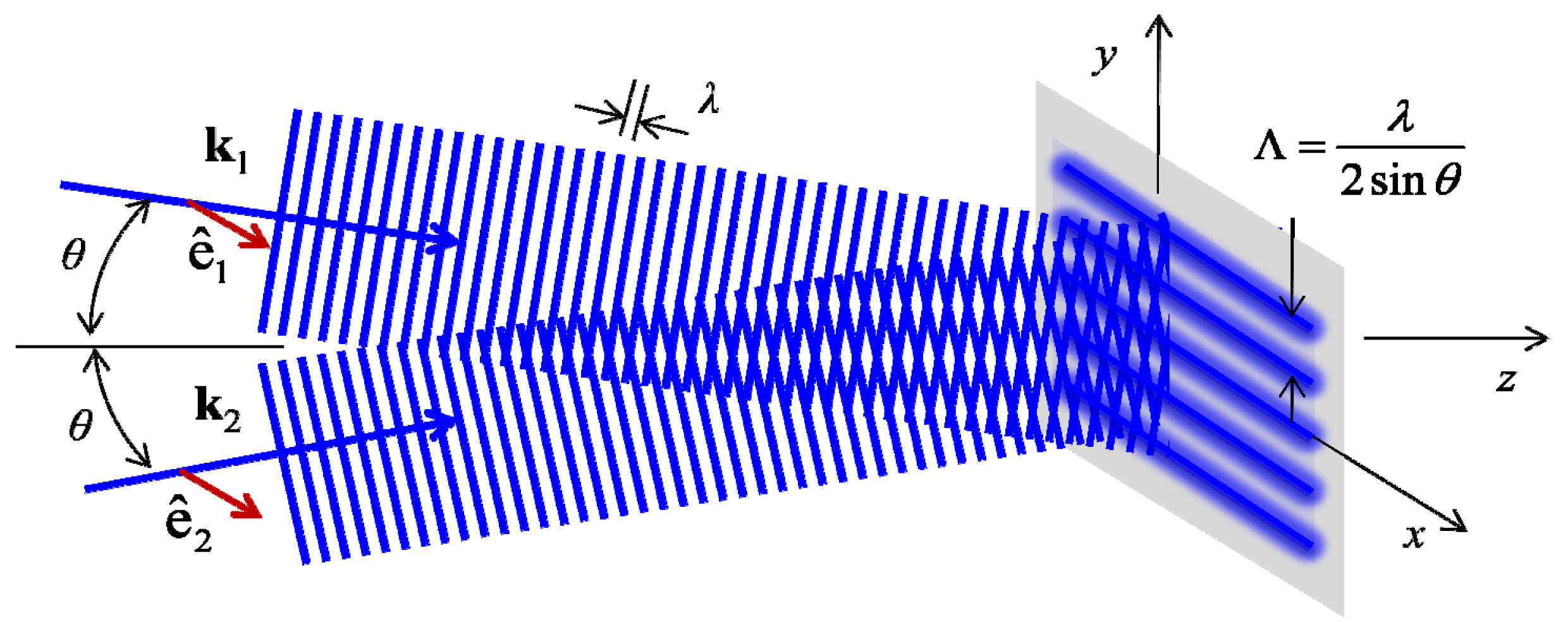
An understanding of MBI may be developed by first considering the familiar interference pattern produced by two linearly-polarized, monochromatic, plane waves derived from a common coherent source. Each plane wave may be defined by Ei(r, t) = Ei cos(ωt − ki·r + Φi)êi, where Ei is the amplitude, ω is the frequency, ki is the wavevector, Φi is the phase, and êi represents the linear polarization vector, and i = 1,2. The interference of the two plane waves produces a one-dimensional (1D) fringe pattern with a periodicity Λ directly proportional to the wavelength λ and inversely proportional to the sine of the sum of the wavevector incidence angles θ with respect to the z axis as depicted in Figure 1.
The total time-independent intensity distribution IT(r) at the intersection of the two waves is expressed as the absolute square of the sum of the amplitudes lT(r) = |E1(r) + E2(r)|2 For the wavevector configuration depicted in Figure 1, the total intensity distribution may be given by
For N interfering beams, the general form of the total time-independent intensity distribution IT(r) may given as
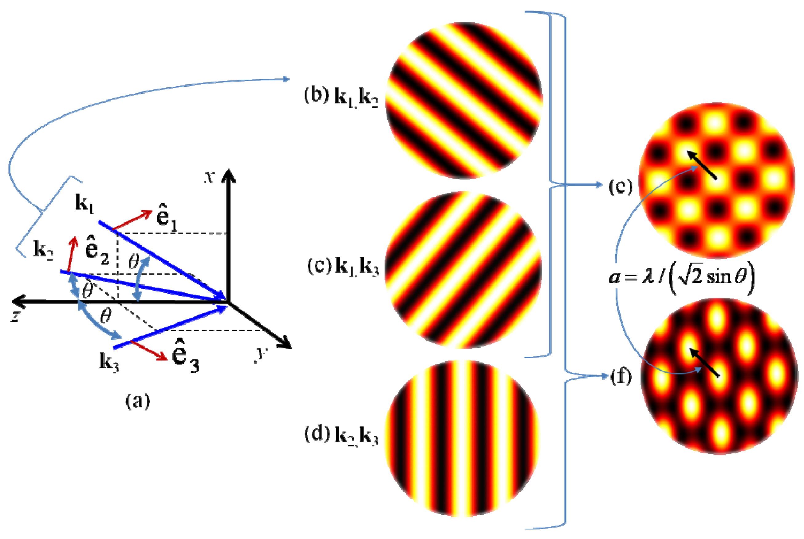
In Equation 2, we see that every beam-pair combination produces a fringe pattern, each defined by a spatial-cosine term with magnitude Vij that contributes to the overall periodic optical-intensity distribution. The orientation and periodicity of these 1D fringe patterns are determined by the relative beam-pair wavevector configurations and angles of incidence, while the relative phase difference determines the position of the fringes along the dimensional axis. In general, three-beam interference produces up to three 1D fringe patterns that combine to form a two-dimensional (2D) pattern as depicted in Figure 2. Four-beam interference provides three-dimensional (3D) patterning with up to six interfering beam pairs. Increasingly complex designs are realized as the number of interfering beams increases and elliptical or circular beam polarizations are considered. Together, the configuration of the wavevectors determines the translational symmetry of the periodic pattern.
The geometry of the unit cell within the periodic pattern further defines the space group symmetry and is determined by the amplitude and polarization of the individual beams. Specifically, the magnitude of each interference coefficient, as defined by Equation 3, is proportional to the product of the amplitudes EiEj and the dot product of the polarization vectors ei · ej for each beam pair. The interference coefficient for each spatial cosine term, in turn, determines the contrast and relative contribution of each beam-pair fringe pattern to the overall periodic distribution. The significance of the individual beam polarizations is demonstrated in Figure 2. By adjusting the relative linear polarizations of the beams defined by k2 and k3, the interference coefficient V23 may be set to a zero value when the two polarization vectors are mutually orthogonal, thereby eliminating the fringe pattern of Figure 2(d) altogether. In this case, assuming equal contrast for the two remaining fringe patterns (V12 = V13), a square lattice is formed with p4m plane group symmetry as depicted in Figure 2(e). Alternatively, for the same wavevector configuration, the relative polarizations may be selected such that all three interference coefficients are equal (V12 = V13 = V23), again combining to form a square lattice, but now with cmm plane group symmetry as depicted in Figure 2(f).
2.1. Advances in Multi-Beam Interference Periodic Patterning
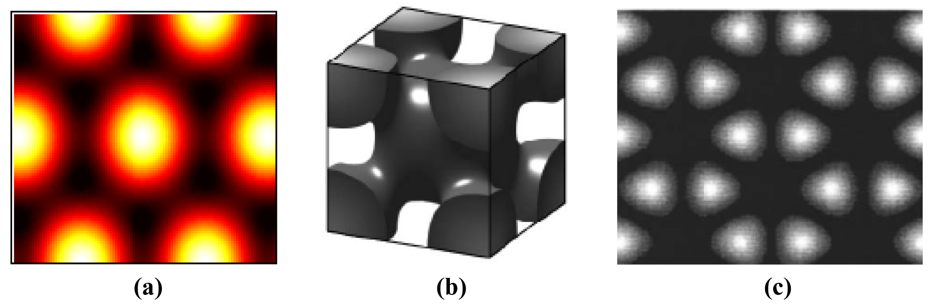
By careful selection of the individual beam wavevectors, amplitudes, and polarizations, research has demonstrated the ability to create all 2D Bravais lattices [10], five of seventeen 2D plane group symmetries [11], and all 3D Bravais lattices via single- [12-15] and multiple-exposure [16,17] techniques. If elliptical polarization is allowed for the individual beams, 4 additional 2D plane group symmetries have been demonstrated for a three-beam configuration [11]. Figure 3(a) demonstrates a 2D hexagonal lattice with p6m plane group symmetry formed by three-beam interference. Figure 3(b) depicts a 3D face-centered-cubic lattice formed by four-beam interference. When the phase of the individual beams is considered, additional control over the interference pattern is possible. For patterns created by four or fewer linearly polarized beams, a change to the relative phase simply translates the interference pattern according to the translational symmetry. If more beams are added, the relative phase difference of the beam pairs will further define the unit cell structure leading to increasingly complex patterning possibilities and space group symmetries [15,18-20]. As an example, a 2D honey-comb structure formed by six-beam interference is depicted in Figure 3(c). Alternatively, a phase shift may be introduced by elliptical polarization in one or more of the interfering beams to produce compound lattices formed by as few as four beams [21-23]. Other quasi-periodic patterns demonstrated using MBI include: 2D structures with 5-, 10-, 12-, and 60-fold symmetries [24,25], connected fcc-like lattices [26], chiral-basis [23] and icosahedral [27] structures, as well as Archimedean-tiled and Penrose lattices [25].
The translational periodicity together with the space group symmetry of the periodic patterns created by MBI determine the geometry of the individual lattice points, or motifs [29]. In some cases, the motif geometry plays a significant role in the performance characteristics of a device fabricated using MBI. For example, the lattice point geometry has been shown to affect the photonic-bandgap characteristics in photonic crystals [30-45], selective plasmonic excitation in plasmonic crystals [46], photonic crystal laser beam pattern [47] and polarization mode control [48], birefringence of photonic crystal fibers [49], cell behavior in tissue engineering [50], tuning of surface textures [51], magnetization switching in periodic magnetic arrays [52], and, negative refraction and superlensing in metamaterials [53,54]. Accordingly, several studies report analytical and computational methods to select individual beam parameters to change the motif orientation and shape [34,42,55,56] from hemispherical to hemielliptical [57]; circular to triangular [58]; as well as, general structures including micro-cavities, micro-bumps, and rectangular bumps [51]. Most recently, research has focused on the exact analytical design and fabrication of motifs with 2D geometries that vary from the shape of an ellipse to that of a rhombus [59].
Given the numerous periodic patterning and motif geometry possibilities afforded by MBI, significant research has focused on maximizing the absolute contrast of the interference pattern by optimized selection of individual beam amplitudes, polarizations, and phases [60-67]. In this effort, the concept of uniform contrast was introduced, in which the relative amplitudes and individual-beam polarizations are optimized to ensure the highest contrast of the pattern as a whole for three- [68-70] and four-beam interference [71,72]. More recently, the conditions for primitive-lattice-vector-direction equal contrasts provided a complete treatment of contrast considerations in three- [73] and four-beam interference [28,74]. While these conditions assume individual control over beam amplitudes and polarizations, recent research suggests that sufficient contrast is still possible, even when beam parameters are perturbed [22] or requirements are simplified by design constraints [59,75].
2.2. Multi-Beam Interference Configurations
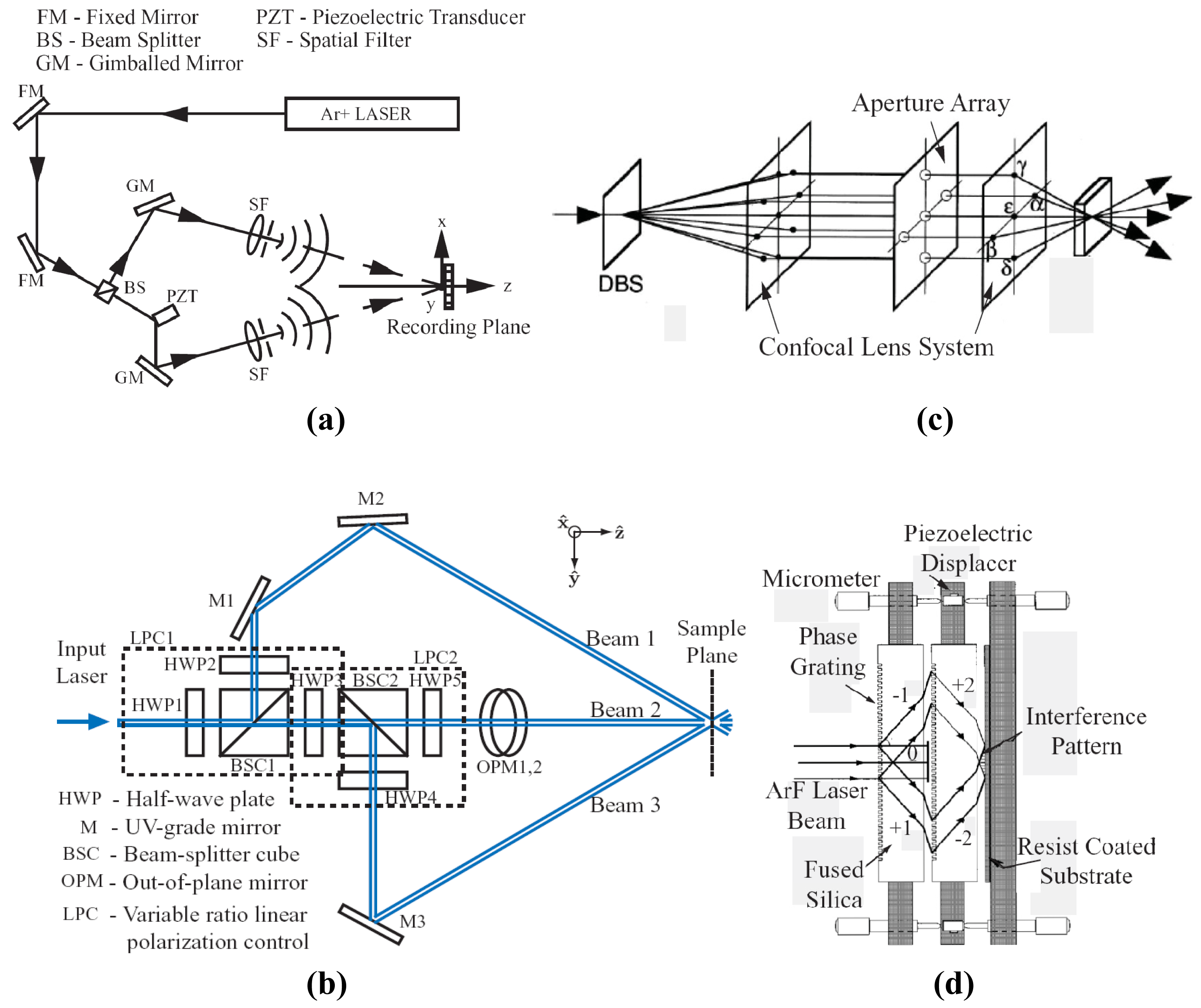
Numerous optical configurations have been employed to generate the multiple beams required for MBI with varying levels of control over beam parameters, interferometric stability, and coherence requirements. These configurations may be broadly categorized as amplitude- or wavefront-splitting methodologies.
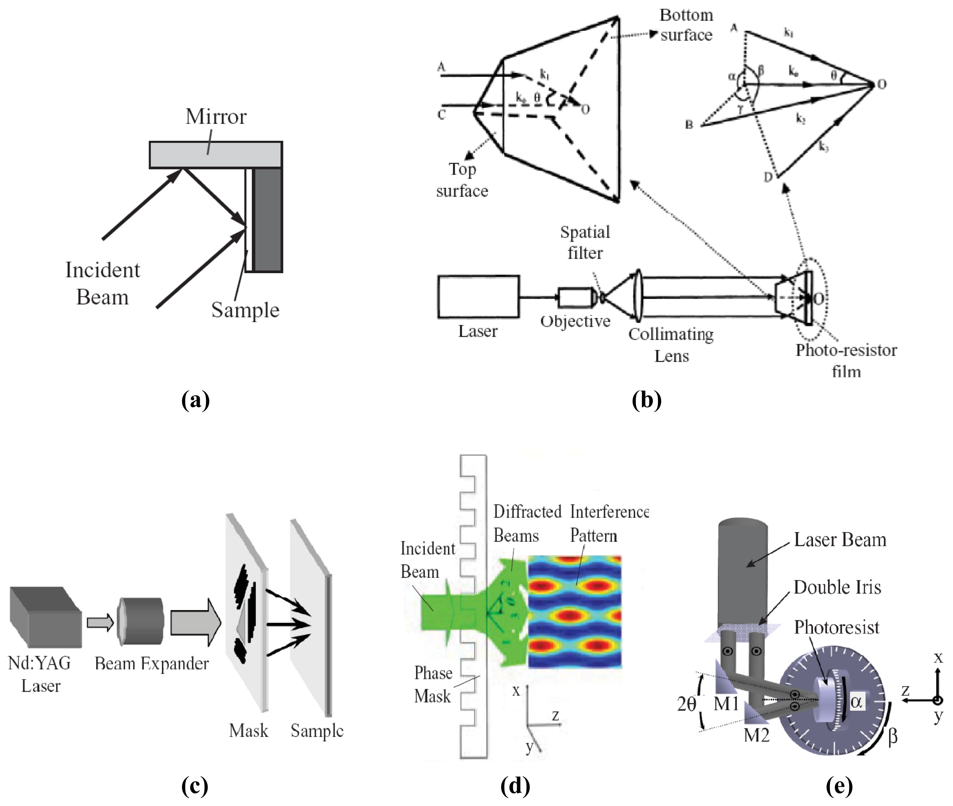
Amplitude-splitting configurations typically divide the single common source beam into two or more beams through the use of beam splitters or other diffractive elements. The beams are then directed to intersect at the plane of interference through the use of mirrors, lens, and/or prisms. An example two-beam configuration to record a 1D grating utilizing a single beam splitter and beam-directing mirrors is depicted in Figure 4(a). In any two-beam configuration, multiple exposures are required to generate more complex 2D and 3D patterns in a photo-sensitive material [76-79]. This is often accomplished by incorporating a rotating sample stage at the recording plane [80-83]. More advanced amplitude splitting systems, such as the configuration depicted in Figure 4(b), allow for the single-exposure of multiple beams [84,85]. Ideally suited for research and development, these configurations often afford the option of individual control over beam amplitude, polarization, and phase, along with a wide range of wavevector configurations and incidence angles [86,87]. For example, using an argon-Ion laser source of 363.8 nm, the configuration in Figure 4(b) can produce five of the seventeen 2D plane group symmetries with a lattice constant ranging from approximately 3.5 μm down to 300 nm. One drawback of these beam-splitting-based configurations is the potential for interferometric instability. Any perturbations to the optical components, optical path lengths, or relative phases of the interfering beams may result in a translation of the pattern or change in the symmetry of the unit cell as discussed earlier.
To lessen these effects, other amplitude-splitting configurations have been developed that rely on gratings to diffract a single incident beam into two or more beams. These beams are, in turn, focused onto the plane of interference by either a lens system as depicted in Figure 4(c) [72,88], beam-directing mirrors [25,89], or cascaded diffractive elements [90,91] such as the achromatic interference lithography configuration depicted in Figure 4(d) [92]. The symmetries formed by the zero- and first-order diffracted beams in Figure 4(c) make this configuration particularly useful in implementing the much-studied five-beam umbrella configuration consisting of a central beam (C-beam) surrounded by four symmetric ambient beams (A-beams) [67,93-96]. For an umbrella configuration, this scheme is particularly useful if the individual beams require specific conditioning, such as different polarizations (e.g., circularly polarized C-beam and linearly polarized A-beams) [97] or phase control [25].
To simplify optical configurations and improve interferometric stability, wavefront-splitting schemes have been developed that divide portions of a single expanded source beam into the multiple beams required for MBI. The most common and widely used wavefront-splitting configuration incorporates a Lloyd's mirror to reflect a portion of an expanded source beam to intersect with the transmitted portion as depicted in Figure 5(a). As early as 1985, a Lloyd's mirror configuration was used as a simple way to fabricate linear grating couplers [100]. Again, multiple exposures are required with this configuration to produce 2D and 3D patterns [101], with one recent report of a Lloyd's mirror capable of producing three beams with 120 degree symmetry [102]. A Lloyd's mirror configuration may also be combined with immersion lithography, further reducing the fringe pattern periodicity to the sub-100 nm range [103].
A second common wavefront-dividing configuration incorporates a specially designed prism to divide and refract the single expanded beam into multiple beams as depicted in Figure 5(b) [104-106]. This prism-based method is particularly useful in implementing the previously discussed umbrella configuration, with expanded options for four or more beams [107]. By selecting a prism with a refractive index matching that of the recording material, refraction-induced asymmetries may be mitigated at the at the prism-sample plane interface. In fact, an index-matching prism element may be also be used in amplitude-splitting configurations, incorporated at the sample plane, to mitigate these same asymmetries, including changes to the individual beam polarizations at the air-photoresist interface [25,108,109].
Diffractive gratings may also be used in a wavefront-dividing scheme in the form of a single diffractive photo-mask. In this configuration, two or more gratings are typically used to diffract a single expanded beam, such that the first order diffracted beams intersect and interfere at the sample plane as depicted in Figure 5(c) [110-115]. In one report, multiple gratings with precisely controlled periods were used to produce compound periodic patterns with a large depth of focus using an achromatic source [19]. If an umbrella configuration is required, the zero-order diffracted beam from a diffractive photo-mask may function as the C-beam [116].
A fourth option for wavefront splitting places a photo mask with a single diffractive optical element in close proximity to the sample plane to produce a near-field self-interference pattern of the zero-, positive-, and negative-diffracted orders as depicted in Figure 5(d) [117-121]. In this example, a 1D phase mask diffracts the incident beam into three interfering beams at the exit of the mask. Multiple exposures of a 1D phase mask may be used to produce complex 3D periodic patterns, such as a woodpile-type structure [122,123]. Alternatively, a multi-layer mask with two orthogonal diffractive gratings [124-126] or a single 2D diffractive optical element [127-130] may be used to produce multiple beams with a single exposure. As a result of the relatively short optical path lengths for the diffracted beams, this method is essentially phase-locked, representing the most interferometrically stable option for MBIL. However, with this advantage does come some disadvantages. As with the previous three wavefront-splitting configurations, control over individual beam amplitudes and polarizations is typically limited, wavevector configurations are generally fixed, and each are sensitive to transverse incoherence. An amplitude-splitting configuration with even-symmetry reflections or diffractions as depicted in Figure 4(a,c,d) may be used to resolve transverse coherence issues, assuming any beam offset is within the transverse coherence length and the spatial coherence meets depth of focus requirements [131,132].
Finally, a fifth wavefront-splitting option is depicted in Figure 5(e), employing a double-iris amplitude mask to define the individual beams, while providing the opportunity for individual beam conditioning and wavevector control [133-135].
2.2. Multi-Beam Interference Lithography and Nano-Electronics
As early as 1970, the fringe patterns formed by two-beam interference were recorded in photoresist, forming a simple, reproducible diffraction grating for use in thin-film waveguides [137]. Two decades later, multiple MBIL exposures were proposed to generate more complex 2D patterns in a photoresist [138]. Since then, a wide range of structures have been recorded via MBIL using near-infrared [129,139-142], visible light [18,31,32,62,88,143-153], ultraviolet (UV) [62,77,78,99,115,154-160], deep-UV [92,101,142,161-163], and extreme-UV sources [164-167].
Today, MBIL is considered a potentially key enabling technology for the ever-increasing demand for smaller feature sizes in optical lithography [4,131,168]. Modern integrated circuits have very regular layouts with an underlying grid pattern that defines the smallest feature size in the integrated circuit. MBIL can be used to define this underlying periodic or quasi-periodic grid-based structure. In this application, MBIL immediately has the advantages of (1) simple optics, (2) large working distances, (3) fast processing, (4) low cost, and (5) extendable to higher resolutions [4,25,169-171].
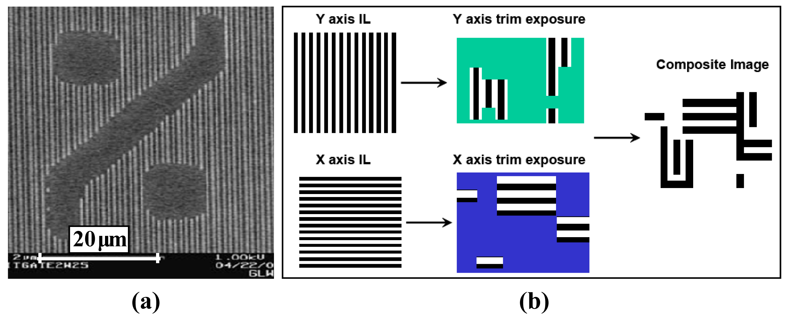
To create functional elements in the periodic pattern defined by MBIL, a second lower spatial-frequency trim exposure may be used to define the non-periodic features using a conventional technique such as projection lithography (PL), thereby easing the diffraction limitations of using PL alone [2,5,172]. As an example, Figure 6(a) depicts a hybrid optical maskless lithography technique demonstrating the use of two-beam interference to form vertical fringes, followed by a second traditional low-pitch PL trim exposure [163]. Similarly, Figure 6(b) demonstrates a multi-step procedure to create more complex composite patterns. Others have combined MBIL with various lithographic techniques including other mask-based techniques (e.g., proximity or contact lithography) [159,173], electron-beam lithography [81,174,175], electron-beam-induced deposition [176], focused ion-beam lithography [155,177], direct laser writing [77,150,178,179], atomic force microscopy nano-indentation [180], and multi-photon polymerization [181-183]. For example, interference lithography has been combined with optical contact lithography to fabricate triple-gate metal-oxide-semiconductor field effect transistors [161]. In another report, interference lithography was used for metal thin-film patterning to fabricate the electrodes and metallization patterns required by modern microelectronic devices [139]. In fact, a recent economic assessment of various lithography choices indicates that a double-exposure technique, optimized by the use of MBIL, is the best choice for low to medium volume products [4]. Future research could make MBIL a preferred component of higher volume production as well.
A wide array of photosensitive materials have been used to record the interference patterns formed by MBIL and include positive resists [115,157,184], negative resists [99,185], hybrid organic-inorganic materials [165,186,187], extreme-UV photoresists [188], silsesquioxane-based photoresists [129], holographic polymer-dispersed liquid crystals [189], amorphous-chalcogenide-semiconductor thin films [190], titanium-containing monomer films [191], red-sensitive photopolymers [145], polyimide foils [51], biocompatible polymers [50], oligomer films [153], and even silica [192] and chalcogenide [193] glasses. In the most general terms, given sufficient optical intensity, an interference pattern may be recorded in or on any material that responds to laser illumination at a given wavelength [160], to include direct writing on metallic surfaces via laser interference metallurgy [194] and direct laser interference patterning of π-conjugated polymers [195].
With the numerous patterning options, simple optical configurations, and opportunities in optical lithography, MBI has found applications across a wide range of technological areas beyond nano-electronics, including photonic crystals, metamaterials, subwavelength structures, optical trapping, and biomedical structures. Thus, a unified review of these broad applications follows.
3. Photonic Crystals
Perhaps the most documented application of MBI and MBIL has been in the formation of photonic crystal (PC) structures and is the subject of more than half of the references included in this review. PC technology has many important possible commercial applications [196,197] with the possibility of lossless control of light propagation at a size scale near the order of the wavelength of light. This technology has the potential to produce the first truly dense integrated photonic circuits and systems (DIPCS). Individual components that are being developed include resonators, antennas, sensors, multiplexers, filters, couplers, and switches. The integration of these components would produce DIPCS to perform functions such as image acquisition, target recognition, image processing, optical interconnections, analog to digital conversion, and sensing. Further, the resulting DIPCS would be very compact in size and highly field portable. Applications using light at telecommunications wavelengths require structures to be fabricated with nano-sized dimensions. Despite the advantages and benefits of using such a technology in commercial devices, a major problem exists: the practical commercial development of PC structures has been very slow.
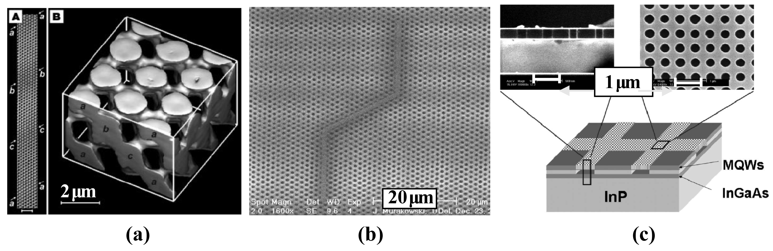
To date, research has not fully developed a methodology for the large-scale and cost-effective integration of these impressive PC-based devices into manufacturable DIPCS. No rapid and inexpensive systematic fabrication procedure has been developed for the reliable and reproducible fabrication of nano-sized PC structures. MBIL has been proposed as one method to overcome this deficiency. In the late 1990s, interference lithography was used to produce 2D [158] PC lattices exhibiting a photonic bandgap and later 3D face-centered cubic [157] PC structures as depicted in Figure 7(a). Since then, MBIL has been extensively studied, optimized, and used to fabricate PCs [109,184,198-203] with ongoing efforts to develop PC-based devices through a combination of lithography techniques such as the PC waveguide depicted in Figure 7(b). In fact, the design rules for MBIL-defined PC waveguide devices have been theoretically defined, when interference lithography is combined with direct laser writing [204]. Recently, nanoscale photonic-crystal-band-edge lasers were fabricated with the use of interference lithography, paving the way for the integration of electrically-driven PC lasers [205] as depicted in Figure 7(c). Other proposed PC-based devices relying on MBIL include optical add-drop multiplexers [206], organic light emitting diodes (LEDs) [207], coupled PC resonator arrays [208], and PC distributed feedback quantum cascade lasers [209].
4. Metamaterials
Like photonic crystals, metamaterial technology offers the control of light propagation, only now at a size scale much smaller than the wavelength of light. Accordingly, metamaterial-based devices have many important possible commercial applications [210-213]. Ultra-compact objective lenses, frequency-doubling devices, parametric amplifiers, electromagnetic cloaking, and parametric oscillators all become possible with metamaterials. The integration of these components would produce DIPCS that are very compact in size and highly field-portable.
In natural materials (as contrasted to metamaterials), atoms are arranged in a regular pattern with periods of approximately half of a nanometer. In these natural materials, the electric field component of the incident light excites the electric dipoles of the material. These dipoles re-radiate with some phase retardation. Thus, the electric relative permittivity εr is not equal to unity. In contrast, the magnetic dipoles do not appreciably interact with the magnetic field component of the incident light. Thus the relative magnetic permeability μr is unity. Metamaterials overcome this lack of magnetic dipole through subwavelength-sized artificial magnetic dipoles (e.g., split-ring resonator structures). The index of refraction, in general, is n = ±(εr μr)1/2. For the case when both εr and μr are less than zero, the refractive index is negative. That is, n = −(εr μr)1/2. The index is not n = +(εr μr)1/2. This result was first reported and discussed by Veselago [214].
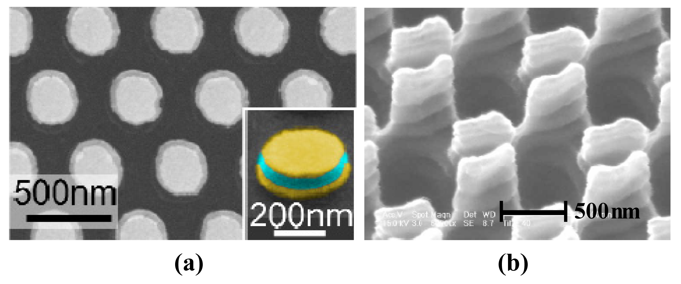
The subwavelength-sized magnetic dipoles needed to make a metamaterial, can be produced by making microscopic split-ring resonators (SRR's). These SRR devices have also been called “slotted-tube resonators” or “loop-gap resonators” in the literature. If SRR devices are produced in subwavelength arrays, they behave as “magnetic atoms” and thus metamaterials become possible. Metamaterials have been successfully developed at microwave frequencies [215-217]. However, the production of metamaterials at optical frequencies has been much more challenging [218,219]. Further, current technologies lack the ability to produce these precise nanostructure devices rapidly and at low cost. Again, MBIL provides a potential solution to this critical shortcoming [220]. To produce a large area split-ring array template for magnetic metamaterials, MBIL has been proposed as a mechanism to form single-slit and double-slit split-ring arrays in 2D triangular and square lattice arrays [221]. Others have used MBIL to demonstrate high-throughput experimental fabrication of metal-dielectric-metal “magnetic atoms” [222,223] as depicted in Figure 8(a), as well as cylindrical nanoshell, U-shaped, and double-split ring resonator array metamaterials [224] as depicted in Figure 8(b). In some cases, MBIL may be used in conjunction with other methods to facilitate the economical fabrication of metamaterials. For example, interference lithography can be used to form a 1D array of trenches to serve as a template for the self-directed assembly of a silver nanocluster metamaterial [225].
5. Subwavelength Structures
Research into micro- and nano-scale subwavelength structures has grown exponentially in the last decade. By utilizing the subwavelength periodic patterns produced by MBIL, numerous important structures can be realized for an increasing number of subwavelength structure applications, including synthesized-index elements, form-birefringent polarization elements, guided-mode resonant elements [226], field-emission devices, plasmonic structures, surface texturing, magnetic nanostructures, and numerous other nanotechnology efforts.
5.1. Synthesized-Index Elements
Synthesized-index elements include 1D and 2D periodic surface structures for use as antireflection surfaces. Simple 1D binary surface-relief gratings on dielectrics can exhibit zero-reflectivity at optical wavelengths [227,228]. For example, interference lithography has been used to record subwavelength gratings on the surface of diffractive beam splitters, reducing surface reflections, thereby improving efficiency [229]. Similarly, MBIL was used to fabricate subwavelength antireflective coatings to improve the performance of optoelectronic LEDs [230]. More recently, subwavelength antireflection patterns were recorded in a Si substrate using interference lithography, providing broadband (250–1,200 nm), wide angle (0–45°) operation [231] as depicted in Figure 9(a). Such antireflection surfaces have been extended to lossy, even metallic, materials [232,233]. 2D crossed gratings have also been implemented to provide polarization-independent antireflection behavior, mimicking the effect of a “moth's eye” [149,234,235]. Periodic and quasi-period surfaces have been widely applied to increase the efficiency of solar cells [236,237]. To this end, interference lithography was recently used to fabricate antireflective gratings on thin-film solar cells [238]. Other example applications include a 100 nm period grating in an amorphous silicon thin film used to stabilize the linear polarization of vertical-cavity surface-emitting laser operating at 850 nm [239], and a critical angle transmission grating facilitated by the use of scanning-beam interference lithography [240].
5.2. Form-Birefringent Polarization Elements
Form-birefringent polarization elements include retardation plates, polarizers, and beam-splitters. Retarders can behave as quarter-waveplates, half-waveplates, full-waveplates, etc. and thus convert linearly polarized light to circular polarization, rotate linear polarization, provide narrowband filtering, etc. Subwavelength grating retarders have been made using MBIL for use in the visible and in infrared regions of the spectrum [241] as depicted in Figure 9(b). Similarly, subwavelength-grating polarizers have also been reported [98]. Two-beam interference lithography has been demonstrated as a highly cost effective fabrication process to generate these subwavelength structures [228].
5.3. Guided-Mode Resonant Elements
Guided-mode resonant gratings are widely utilized for their very narrowband filter characteristics [242-244]. Such subwavelength-grating filters represent important devices in dense-wavelength-division multiplexed communications and in chemical, biological, toxicological, and environmental sensing applications. Recently, broadband versions of these resonant gratings have also been demonstrated [245].
5.4. Field Emission Devices
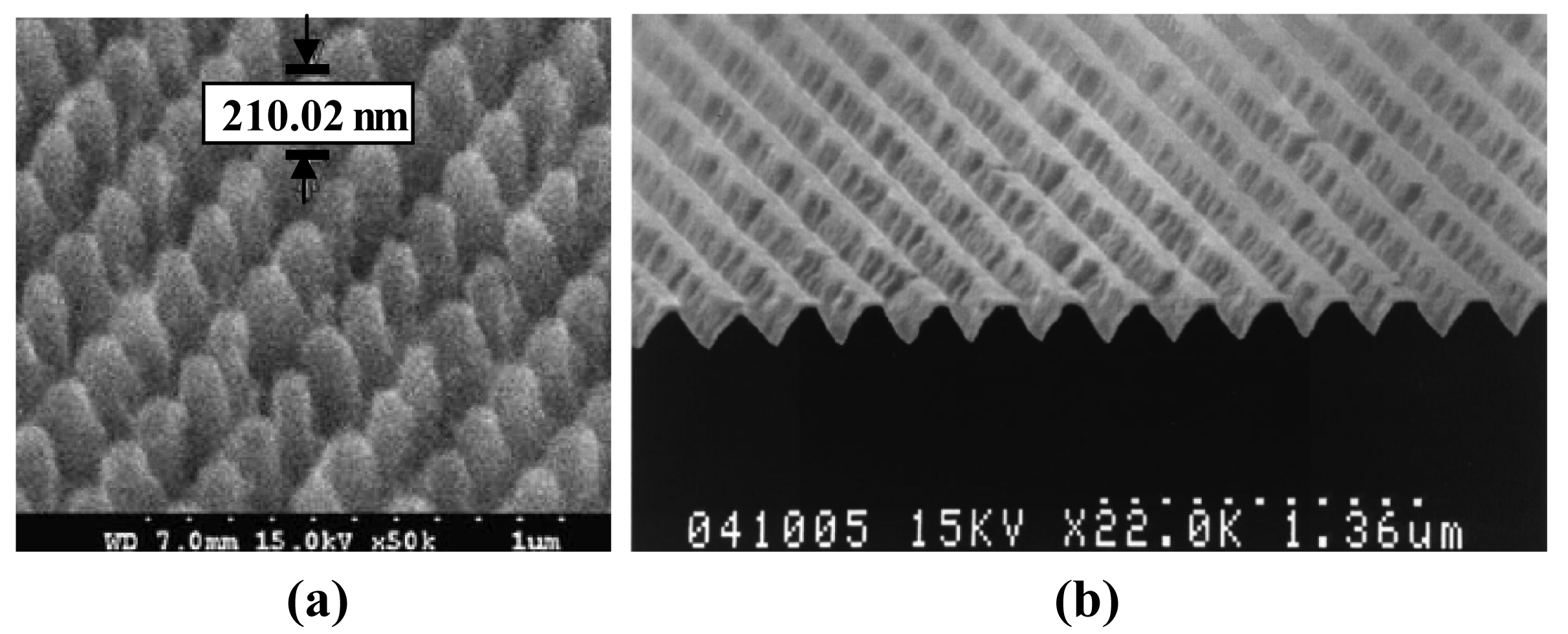
The process of field emission ejects electrons from a metal surface or a doped semiconductor material under the influence of an applied electric field. Traditionally, field emission is generated from micro-structured tips used as the cathodes for electron extraction. Field emission devices have found applications in field emission displays, vacuum microelectronics, satellite subsystems, mass spectrometers, and even electrodynamic space tethers [246,247]. As early as 1995, interference lithography was used to manufacture high density micro-field emitter arrays with submicron emitter spacing to improve field emission display performance and reduce manufacturing costs [156,248]. Recent efforts have focused on the use of interference lithography, combined with catalytic etching, to produce the nanocones used in field emission as depicted in Figure 10(a), potentially eliminating the need for other more complicated lithography techniques [249]. Others have employed MBIL to aid in the production of carbon nanotubes as depicted in Figure 10(b) that could prove useful in field emission display applications [250].
5.5. Plasmonic Structures
Surface plasmon resonances occur for a range of frequencies when an electromagnetic field excites oscillations of free electrons on the surface of metallic nanostructures [251]. Near-field coupling effects on the plasmon resonance of these metal nanostructures, called localized surface plasmons, can be used in biosensing applications, surface enhanced Raman spectroscopy, and novel photonic devices [82,252,253]. The mechanism of plasmonic resonance is directly related to the refractive index variation in the metallic film nanostructures, commonly fabricated using self-assembly methods. As an alternative to self-assembly methods, MBIL has been used as a mechanism to produce plasmonic metallic nanostructures including silver dot arrays [251,254], gold particle arrays [82,252], and bimetallic dot structures [46,253] depicted in Figure 11(a–c) respectively.
5.6. Surface Texturing
Surface patterning at the micro- and nano-scale has been the subject of much study, with applications across numerous areas, including microelectromechanical systems, automotives, aviation, defense, and biological areas [194,255]. Laser surface texturing using MBI is of particular interest to tribology technologies including textured surfaces for mechanical seals, piston rings, and thrust bearings. In one study, laser interference metallurgy was employed to improve lubrication film lifetimes and the tribological behavior of various surface textured materials as depicted in Figure 12(a) [194]. Others have studied the wetting properties and superhydrophobicity of surfaces, patterned by laser interference, for such applications as corrosion inhibition, microfluidic technology, self-cleaning window glass, and evaporation-driven nanopatterning [151,256]. Similarly, interference patterning has been used to create biomemetic structures as depicted in Figure 12(b), mimicking natural sub-micron patterns [257] such as bone material and shells exhibiting advantageous mechanical stability and dynamic surface properties [255].
5.7. Magnetic Nanostructures
Magnetic nanostructures, often called “nanomagnets,” have been proposed as an alternative technology for information storage [258,259]. In this application, discrete nanomagnets with uniaxial magnetic anisotropy store binary information when magnetized in one of two possible antiparallel directions. To generate these magnetic nanostructures, interference lithography has been used to generate a nanoscale array of dots that are, in turn, transferred to a magnetic film using ion beam etching as depicted in Figure 13(a) [258,259]. Others have employed interference lithography in the fabrication of cobalt magnetic arrays for use in magnetic random access memory devices as depicted in Figure 13(b) [260]. Most recently, MBIL was used to create magnetic patterns in Co/Pd multilayer systems with favorable magnetic properties as depicted in Figure 13(c) [261].
6. Optical Trapping
The periodic pattern produced by MBI need not always be recorded in a photosensitive material. For example, the light intensity distribution produced by MBI may be used directly as optical traps. Traditionally, optical trapping relies on the increased electrical field associated with the localized optical intensity of a focused beam. A dielectric particle is, in turn, guided by the increased electric field force to the point of the highest light intensity. By this mechanism, optical traps have been used to manipulate a range of particles including polymer spheres, metallic particles, and biological specimens [262]. Recently, techniques to manipulate suspended micro- and nano-scale particles have been realized through the use of holographic optical tweezers, trapping multiple objects simultaneously [263]. In this application, the focused beams are replaced by computer-defined beam arrays generated by a spatial light modulator. Using this method, sophisticated algorithms have been developed to provide updates to the computer generated hologram to control dynamically the orientation of the multiple trapped particles. Recently, this techniques was used to control and study rod-shaped bacteria [264] and zeolite L crystals [265].
As an alternative to computer generated holographic optical tweezers, MBI may provide similar optical arrays along with dynamic control of light intensity and orientations in two- and three dimensions, easing the requirement for complicated computer control algorithms. MBI optical trapping was first realized in the 1990's with a two-beam interferometric trap to hold polystyrene beads of a few microns in diameter as depicted in Figure 14(a) [266]. Later, 2D and 3D interference patterns were used to trap, sort, and manipulate trapped particles on a small scale using focused interfering beams [267-271] as depicted in Figure 14(c). Recently, large-area 3D arrays of optical traps have been demonstrated through the use of MBI, without the need for iterative computational algorithms, as depicted in Figure 14(b) [272].
7. Biomedical Structures
Biomedical structures that are periodic or quasi-periodic in one-, two-, and three-dimensions are critically important in a wide variety of areas. Some representative example applications are described here to enable gauging the impact that they have in biomedicine. In regenerating nerves, arrays of microchannels are needed to guide nerve growth [274]. In facilitating bone regrowth, periodic meshes are needed to retain and sequester bone morphogenetic protein. This process reduces protein dose by localizing the morphogenetic stimulus [275]. In the forming, maintaining, and repairing of tissue, engineered surfaces are needed that present controlled densities of peptides to direct the assembly of extracellular matrices [276]. In measuring the strength of cell adhesion to the extracellular matrix, meshes are needed to control the size and position of cells to be able to determine the individual contributions of the various structures present [277]. In identifying genetic biomarkers for human disease, high density microarrays are needed for the detection of dozens of polymorphisms in a single analysis. For example, 11 micron square positions are used so that highly redundant oligonucleotide probes can ensure robustness [278]. In studying the functions of a cell (gene expression, adhesion, migration, proliferation, and differentiation), micropatterning of the cells is needed since the cell functions are affected by the microscale and nanoscale environment [279]. In enhancing bone formation in vivo, it is necessary to microstructure the titanium implant surfaces. For example, 100 μm cavities are found to produce osteoblast attachment and growth [280]. In the controlled delivery of insulin, a permeable membrane mesh is needed that allows insulin and nutrients to pass through while blocking larger immune cells, T-cells, and antigen-presenting cells.
Common to all of these biomedical applications is the requirement for appropriate periodic or quasi-periodic structures that can be made by MBIL. This fact has led several to turn to MBIL for numerous biomedical applications in recent years. For example, micro-structured particles have been produced using a combination of MBIL and stop-flow lithography as depicted in Figure 15(a) with several potential applications including cell growth, tissue engineering, and biosensors [153]. To immobilize proteins in a square array of anchor sites, nano-scale lattices were formed by interference lithography. This application will assist in the analysis of biomaterials and the study of interactions of living cells with biomolecules [281,282]. As an example, Figure 15(b) depicts a scanning electron microscope image of square lattice of submicron domains to provide selective absorption of protein fibronectin, leading to advanced studies in the influence of protein organization in adhesion complex formation and function. In the development of neural prosthetic devices, phase mask interference lithography was used to fabricate 3D hydrogels with controlled geometries and sub-micron feature sizes as depicted in Figure 15(c). This application could lead to advances in drug delivery, tissue engineering and improved material-device interactions [50]. In the field of antibacterial research, MBIL was used to create a 2D pore-array to immobilize silver nanoparticles, known for their antibacterial properties. In a study of this application, the fabricated antibacterial nanocomposition proved effective against the E. coli bacteria [283]. Based on these recent examples, MBIL could become an important tool in the development of the next generation of biomedical structures.
8. Conclusions
MBI and MBIL have the potential to impact significantly a wide variety of applications. Numerous periodic and quasi-periodic patterns with specific space group symmetries and motif geometries are now possible by careful selection of individual beam amplitudes, polarizations, wavevector configurations, and phases. These same parameters also enable the optimization of the contrast of the resulting pattern, providing lithographically useful patterning possibilities. As such, several optical configurations and lithographic techniques have been developed to incorporate MBIL, providing the potential for low-cost, wafer-scale, simple, and fast lithographic fabrication. Of obvious interest to the nano-electronics industry, MBI and MBIL have found additional applications in the areas of photonic crystals, metamaterials, subwavelength structures, optical trapping, and biomedical structures
The potential importance of MBI continues to grow with the ever-increasing interest in nano-technologies. More research and development are needed to bring MBI into mainstream applications, including combining MBIL with other conventional processes to produce functional integrated devices. In doing so, MBIL may provide the technology necessary to continue to meet the predictions of Moore's law in the IC industry, while finding additional applications in an increasing list of micro- and nano-technology fields.


Acknowledgments
This research was supported in part by Grant No. ECCS 0925119 from the National Science Foundation.
References
- Cressler, J.D. Silicon Earth: Introduction to the Microelectronics and Nanotechnology Revolution; Cambridge University Press: New York, NY, USA, 2009. [Google Scholar]
- Rothschild, M. Nanopatterning with UV optical lithography. Mater. Res. Soc. Bull. 2005, 30, 942–946. [Google Scholar]
- Jang, J.H.; Ullal, C.K.; Maldovan, M.; Gorishnyy, T.; Kooi, S.; Koh, C.Y.; Thomas, E.L. 3D micro- and nanostructures via interference lithography. Adv. Funct. Mater. 2007, 17, 3027–3041. [Google Scholar]
- Jhaveri, T.; Strojwas, A.; Pileggi, L.; Rovner, V. Economic assessment of lithography strategies for the 22 nm technology node. Proc. SPIE 2009, 7488, 74882Y. [Google Scholar]
- Smith, B.W. Alternative optical technologies: More than curiosities? Proc. SPIE 2009, 7274, 727402. [Google Scholar]
- Solak, H.H. Nanolithography with coherent extreme ultraviolet light. J. Phys. D Appl. Phys. 2006, 39, R171–R188. [Google Scholar]
- Moon, J.H.; Ford, J.; Yang, S. Fabricating three-dimensional polymeric photonic structures by multi-beam interference lithography. Polym. Adv. Technol. 2006, 17, 83–93. [Google Scholar]
- Xia, D.; Ku, Z.; Lee, S.C.; Brueck, S.R.J. Nanostructures and functional materials fabricated by Interferometric lithography. Adv. Mater. 2011, 23, 147–179. [Google Scholar]
- Saleh, B.E.A.; Teich, M.C. Fundamentals of Photonics; John Wiley & Sons, INC.: New York, NY, USA, 1991. [Google Scholar]
- Cai, L.Z.; Yang, X.L.; Wang, Y.R. Formation of a microfiber bundle by interference of three noncoplanar beams. Opt. Lett. 2001, 26, 1858–1860. [Google Scholar]
- Mao, W.D.; Zhong, Y.C.; Dong, J.W.; Wang, H.Z. Crystallography of two-dimensional photonic lattices formed by holography of three noncoplanar beams. J. Opt. Soc. Am. B 2005, 22, 1085–1091. [Google Scholar]
- Cai, L.Z.; Yang, X.L.; Wang, Y.R. All fourteen Bravais lattices can be formed by interference of four noncoplanar beams. Opt. Lett. 2002, 27, 900–902. [Google Scholar]
- Turberfield, A.J. Photonic crystals made by holographic lithography. MRS Bull. 2001, 26, 632–636. [Google Scholar]
- Mei, D.; Cheng, B.; Hu, W.; Li, Z.; Zhang, D. Three-dimensional ordered patterns by light interference. Opt. Lett. 1995, 20, 429–431. [Google Scholar]
- Petsas, A.I.; Coates, A.B.; Grynberg, G. Crystallography of optical lattices. Phys. Rev. A 1994, 50, 5173–5189. [Google Scholar]
- Ono, Y.; Ochi, T. All fourteen Bravais lattices can be fabricated by triple exposure of two-beam interference fringes. Proc. SPIE 2006, 6327, 632709. [Google Scholar]
- Dwivedi, A.; Xavier, J.; Joseph, J.; Singh, K. Formation of all fourteen Bravais lattices of three-dimensional photonic crystal structures by a dual beam multiple-exposure holographic technique. Appl. Opt. 2008, 47, 1973–1980. [Google Scholar]
- Wu, L.J.; Zhong, Y.C.; Wong, K.S.; Wang, G.P.; Yuan, L. Fabrication of hetero-binary and honeycomb photonic crystals by one-step holographic lithography. Appl. Phys. Lett. 2006, 88, 09115. [Google Scholar]
- Solak, H.H. Space-invariant multiple-beam achromatic EUV interference lithography. Microelectron. Eng. 2005, 78-79, 410–416. [Google Scholar]
- Jimenez-Ceniceros, A.; Trejo-Duran, M.; Alvarado-Mendez, E.; Castano, V.M. Extinction zones and scalability in N-beam interference lattices. Opt. Commun. 2010, 283, 362–367. [Google Scholar]
- Mao, W.D.; Dong, J.W.; Zhong, Y.C.; Liang, G.Q.; Wang, H.Z. Formation principles of two-dimensional compound photonic lattices by one-step holographic lithography. Opt. Express 2005, 13, 2994–2999. [Google Scholar]
- Chan, T.Y.M.; Toader, O.; John, S. Photonic band gap templating using optical interference lithography. Phys. Rev. E 2005, 71, 046605. [Google Scholar]
- Dedman, E.R.; Sharp, D.N.; Turberfield, A.J.; Blanford, C.F.; Denning, R.G. Photonic crystals with a chiral basis by holographic lithography. Photonics Nanostruct. 2005, 3, 79–83. [Google Scholar]
- Lai, N.D.; Lin, J.H.; Hsu, C.C. Fabrication of highly rotational symmetric quasi-periodic structures by multiexposure of a three-beam interference technique. Appl. Opt. 2007, 46, 5645–5648. [Google Scholar]
- Juodkazis, S.; Mizeikis, V.; Misawa, H. Three-dimensional microfabrication of materials by femtosecond lasers for photonics applications. J. Appl. Phys. 2009, 106, 051101. [Google Scholar]
- Zaccaria, R.P.; Shoji, S.; Sun, H.B.; Kawata, S. Multi-shot interference approach for any kind of Bravais lattice. Appl. Phys. B 2008, 93, 251–256. [Google Scholar]
- Tam, W.Y. Icosahedral quasicrystals by optical interference holography. Appl. Phys. Lett. 2006, 89, 251111. [Google Scholar]
- Stay, J.L.; Gaylord, T.K. Conditions for primitive-lattice-vector-direction equal contrasts in four-beam-interference lithography. Appl. Opt. 2009, 48, 4801–4813. [Google Scholar]
- Ullal, C.K.; Maldovan, M.; Wohlgemuth, M.; Thomas, E.L.; White, C.A.; Yang, S. Triply periodic bicontinuous structures through interference lithography: A level-set approach. J. Opt. Soc. Am. A 2003, 20, 948–954. [Google Scholar]
- Yang, X.L.; Cai, L.Z.; Wang, Y.R.; Dong, G.Y.; Shen, X.X.; Meng, X.F.; Hu, Y. Large complete bandgaps in a two-dimensional square photonic crystal with isolated single-atom dielectric rods in air. Nanotechnology 2008, 19, 025201–025201. [Google Scholar]
- Moon, J.H.; Pine, D.J.; Yang, S.-M. Fabrication of two-dimensional photonic crystals of non-spherical atoms by holographic lithography. Proceedings of Photonic Crystal Materials and Nanostructures, Strasbourg, France, 27–29 April 2004; pp. 95–99.
- Quinonez, F.; Menezes, J.W.; Cescato, L.; Rodriguez-Esquerre, V.F.; Hernandez-Figueroa, H.; Mansano, R.D. Band gap of hexagonal 2D photonic crystals with elliptical holes recorded by interference lithography. Opt. Express 2006, 14, 4873–4879. [Google Scholar]
- Hung, Y., Jr.; Lee, S.-L.; Pan, Y.-T. Photonic bandgap analysis of photonic crystal slabs with elliptical holes and their formation with laser holography. J. Opt. 2010, 12, 015102. [Google Scholar]
- Ao, X.; He, S. Two-stage design method for realization of photonic bandgap structures with desired symmetries by interference lithography. Opt. Express 2004, 12, 978–983. [Google Scholar]
- Chanda, D.; Abolghasemi, L.; Herman, P.R. Numerical band calculation of holographically formed periodic structures with irregular motif. Proc. SPIE 2006, 6128, 61281E. [Google Scholar]
- Qiu, M.; He, S. Optimal design of a two-dimensional photonic crystal of square lattice with a large complete two-dimensional bandgap. J. Opt. Soc. Am. B 2000, 17, 1027–1030. [Google Scholar]
- Qi, L.M.; Yang, Z.Q.; Gao, X.; Liu, W.X.; Liang, Z. Research on three types of rhombus lattice photonic band structures. J. Electromagn. Waves Appl. 2008, 22, 1155–1164. [Google Scholar]
- Pu, Y.-Y.; Liang, G.-Q.; Mao, W.-D.; Dong, J.-W.; Wang, H.-Z. Fabrication of two-dimensional photonic crystals with triangular rods by single-exposure holographic lithography. Chin. Phys. Lett. 2007, 24, 983–985. [Google Scholar]
- Cai, L.Z.; Dong, G.Y.; Feng, C.S.; Yang, X.L.; Shen, X.X.; Meng, X.F. Holographic design of a two-dimensional photonic crystal of square lattice with a large two-dimensional complete bandgap. J. Opt. Soc. Am. B 2006, 23, 1708–1711. [Google Scholar]
- Wang, R.; Wang, X.-H.; Gu, B.-Y.; Yang, G.-Z. Effects of shapes and orientations of scatterers and lattice symmetries on the photonic band gap in two-dimensional photonic crystals. J. Appl. Phys. 2001, 90, 4307–4313. [Google Scholar]
- Cai, L.Z.; Shen, X.X.; Yang, X.L.; Dong, G.Y.; Meng, X.F.; Xu, X.F.; Wang, Y.R. Holographic design of hexagonal photonic crystals of irregular columns with large full band gap. Opt. Commun. 2006, 267, 305–309. [Google Scholar]
- Yang, X.L.; Cai, L.Z.; Wang, Y.R.; Feng, C.S.; Dong, G.Y.; Shen, X.X.; Meng, X.F.; Hu, Y. Optimization of band gap of photonic crystals fabricated by holographic lithography. Europhys. Lett. 2008, 81, 14001. [Google Scholar]
- Chien, C.W.; Lee, Y.C.; Lee, P.S.; Chang, J.Y.; Chen, J.C. Analysis of a two-dimensional photonic bandgap structure fabricated by an interferometric lithographic system. Appl. Opt. 2007, 46, 3196–3204. [Google Scholar]
- Ohlinger, K.; Lin, Y.K.; Qualls, J.S. Maximum and overlapped photonic band gaps in both transverse electric and transverse magnetic polarizations in two-dimensional photonic crystals with low symmetry. J. Appl. Phys. 2009, 106, 063520. [Google Scholar]
- Li, Z.-Y.; Wang, J.; Gu, B.Y. Full band gap in fcc and bcc photonic band gaps structure: Non-spherical atom. J. Phys. Soc. Jpn. 1998, 67, 3288–3291. [Google Scholar]
- Kang, H.K.; Lee, K.H.; Wong, C.C.; Romanato, F. ID to 2D transitional structure of plasmonic crystals: fabrication and characterization. Appl. Phys. B 2009, 97, 671–677. [Google Scholar]
- Noda, S. Photonic crystal lasers-ultimate nanolasers and broad-area coherent lasers. J. Opt. Soc. Am. B Opt. Phys. 2010, 27, B1–B8. [Google Scholar]
- Noda, S.; Yokoyama, M.; Imada, M.; Chutinan, A.; Mochizuki, M. Polarization mode control of two-dimensional photonic crystal laser by unit cell structure design. Science 2001, 293, 1123–1125. [Google Scholar]
- Hu, B.; Lu, M.; Li, W.; Zou, K.; Zhou, Z.; Lin, A.; Li, N. High birefringent rhombic-hole photonic crystal fibers. Appl. Opt. 2010, 49, 6098–6101. [Google Scholar]
- Jang, J.; Jhaveri, S.J.; Rasin, B.; Koh, C.; Ober, C.K.; Thomas, E.L. Three-dimensionally-patterned submicrometer-scale hydrogel/air networks that offer a new platform for biomedical applications. Nano Lett. 2008, 8, 1456–1460. [Google Scholar]
- Huang, J.; Beckemper, S.; Gillner, A.; Wang, K. Tunable surface texturing by polarization-controlled three-beam interference. J. Micromech. Microeng. 2010, 20, 095004. [Google Scholar]
- Vavassori, P.; Donzelli, O.; Metlushko, V.; Grimsditch, M.; Ilic, B.; Neuzil, P.; Kumar, R. Magnetic switching in submicron-scale periodic magnetic arrays. J. Appl. Phys. 2000, 88, 999–1003. [Google Scholar]
- Tang, Z.X.; Peng, R.W.; Fan, D.Y.; Wen, S.C.; Zhang, H.; Qian, L.J. Absolute left-handed behaviors in a triangular elliptical-rod photonic crystal. Opt. Express 2005, 13, 9796–9803. [Google Scholar]
- Shen, X.X.; Yang, X.L.; Cai, L.Z.; Dong, G.Y.; Meng, X.F.; Xu, X.F.; Wang, Y.R. Negative refractions in two-dimensional photonic crystals formed by holographic lithography. Opt. Express 2007, 15, 8003–8009. [Google Scholar]
- Yuan, L.; Wang, G.P.; Huang, X.K. Arrangements of four beams for any Bravais lattice. Opt. Lett. 2003, 28, 1769–1771. [Google Scholar]
- Li, E.B.; Xi, J.T.; Chicharo, J. Predication of multi-dimensional photonic crystal structures generated by multi-beam interference in holographic lithography. Smart Mater. Struct. 2006, 15, 158–164. [Google Scholar]
- Do, D.B.; Lai, N.D.; Wu, C.Y.; Lin, J.H.; Hsu, C.C. Fabrication of ellipticity-controlled microlens arrays by controlling the parameters of the multiple-exposure two-beam interference technique. Appl. Opt. 2011, 50, 579–585. [Google Scholar]
- Menezes, J.W.; Cescato, L. Recording different geometries of 2D hexagonal photonic crystals by choosing the phase between two-beam interference exposures. Opt. Express 2006, 14, 8578–8583. [Google Scholar]
- Burrow, G.M.; Gaylord, T.K. Constrained parametric optimization of point geometries in multi-beam-interference lithography. Proceedings of Frontiers in Optics 2010, Rochester, NY, USA, 27 October 2010.
- Yang, X.L.; Cai, L.Z.; Liu, Q. Polarization optimization in the interference of four umbrellalike symmetric beams for making three-dimensional periodic microstructures. Appl. Opt. 2002, 41, 6894–6900. [Google Scholar]
- Su, H.M.; Zhong, Y.C.; Wang, X.; Zheng, X.G.; Xu, J.F.; Wang, H.Z. Effects of polarization on laser holography for microstructure fabrication. Phys. Rev. E 2003, 67, 056619. [Google Scholar]
- Fernandez, A.; Decker, J.Y.; Herman, S.M.; Phillion, D.W.; Sweeney, D.W.; Perry, M.D. Methods for fabricating arrays of holes using interference lithography. J. Vac. Sci. Technol. B 1997, 15, 2439–2443. [Google Scholar]
- Fernandez, A.; Phillion, D.W. Effects of phase shifts on four-beam interference patterns. Appl. Opt. 1998, 37, 473–478. [Google Scholar]
- Ellman, M.; Rodriguez, A.; Perez, N.; Echeverria, M.; Verevkin, Y.K.; Peng, C.S.; Berthou, T.; Wang, Z.; Olaizola, S.M.; Ayerdi, I. High-power laser interference lithography process on photoresist: Effect of laser fluence and polarisation. Appl. Surf. Sci. 2009, 255, 5537–5541. [Google Scholar]
- Stay, J.L.; Gaylord, T.K. Contrast in four-beam-interference lithography. Opt. Lett. 2008, 33, 1434–1436. [Google Scholar]
- Chanda, D.; Abolghasemi, L.E.; Herman, P.R. Single laser exposure fabrication of diamond-like 3-dimensional photonic crystal microstructures using circularly polarized light. Appl. Phys. A 2008, 93, 33–37. [Google Scholar]
- Meisel, D.C.; Wegener, M.; Busch, K. Three-dimensional photonic crystals by holographic lithography using the umbrella configuration: symmetries and complete photonic band gaps. Phys. Rev. B 2004, 70, 165104. [Google Scholar]
- Cai, L.Z.; Yang, X.L.; Wang, Y.R. Interference of three noncoplanar beams: Patterns, contrast and polarization optimization. J. Mod. Opt. 2002, 49, 1663–1672. [Google Scholar]
- Cai, L.Z.; Yang, X.L. Interference of circularly polarized light: contrast and application in fabrication of three-dimensional periodic microstructures. Opt. Laser Technol. 2002, 34, 671–674. [Google Scholar]
- Yang, X.L.; Cai, L.Z. Wave design of the interference of three noncoplanar beams for microfiber fabrication. Opt. Commun. 2002, 208, 293–297. [Google Scholar]
- Yang, X.L.; Cai, L.Z. Wave design and polarization optimization in the interference of four non-coplanar beams for making three-dimensional periodical microstructures. J. Mod. Opt. 2003, 50, 1445–1453. [Google Scholar]
- Yang, X.L.; Cai, L.Z.; Wang, Y.R.; Liu, Q. Interference of four umbrellalike beams by a diffractive beam splitter for fabrication of two-dimensional square and trigonal lattices. Opt. Lett. 2003, 28, 453–455. [Google Scholar]
- Stay, J.L.; Gaylord, T.K. Three-beam-interference lithography: Contrast and crystallography. Appl. Opt. 2008, 47, 3221–3230. [Google Scholar]
- Stay, J.L. Multi-Beam-Interference-Based Methodology for the Fabrication of Photonic Crystal Structures. Ph.D. Thesis, Electrical and Computer Engineering, Georgia Institute of Technology, Atlanta, GA, USA, 2009. [Google Scholar]
- Salaun, M.; Audier, M.; Duneau, M.; Delyon, F. Holographic lithography of a two-dimensional hexagonal structure: effect of beam polarization. Appl. Surf. Sci. 2007, 254, 850–854. [Google Scholar]
- Lasagni, A.F.; Dajun, Y.; Das, S. Layer-by-layer interference lithography of three-dimensional microstructures in SU-8. Adv. Eng. Mater. 2009, 11, 408–411. [Google Scholar]
- Pang, L.; Nakagawa, W.; Fainman, Y. Fabrication of two-dimensional photonic crystals with controlled defects by use of multiple exposures and direct write. Appl. Opt. 2003, 42, 5450–5456. [Google Scholar]
- Pati, G.S.; Heilmann, R.K.; Konkola, P.T.; Joo, C.; Chen, C.G.; Murphy, E.; Schattenburg, M.L. Generalized scanning beam interference lithography system for patterning gratings with variable period progressions. J. Vac. Sci. Technol. B 2002, 20, 2617–2621. [Google Scholar]
- Gutierrez-Rivera, L.E.; Cescato, L. SU-8 submicrometric sieves recorded by UV interference lithography. J. Micromech. Microeng. 2008, 18, 115003. [Google Scholar]
- Gauthier, R.C.; Mnaymneh, K.W. Design of photonic band gap structures through a dual-beam multiple exposure technique. Opt. Laser Technol. 2004, 36, 625–633. [Google Scholar]
- Moormann, C.; Bolten, J.; Kurz, H. Spatial phase-locked combination lithography for photonic crystal devices. Proceedings of 29th International Conference on Micro and Nano Engineering, Delft, The Netherlands, 22–25 September 2003; pp. 417–422.
- Lee, F.Y.; Fung, K.H.; Tang, T.L.; Tam, W.Y.; Chan, C.T. Fabrication of gold nano-particle arrays using two-dimensional templates from holographic lithography. Curr. Appl. Phys. 2009, 9, 820–825. [Google Scholar]
- Dyachenko, P.N.; Karpeev, S.V.; Fesik, E.V.; Miklyaev, Y.V.; Pavelyev, V.S.; Malchikov, G.D. The three-dimensional photonic crystals coated by gold nanoparticles. Opt. Commun. 2011, 284, 885–888. [Google Scholar]
- MacLeod, B.D.; Kelsey, A.F.; Leclerc, M.A.; Resler, D.P.; Liberman, S.; Nole, J.P. Fully automated interference lithography. Proceedings of Emerging Lithographic Technologies VI, Santa Clara, CA, USA, 5–7 March 2002; pp. 910–921.
- Rodriguez, A.; Echeverria, M.; Ellman, M.; Perez, N.; Verevkin, Y.K.; Peng, C.S.; Berthou, T.; Zuobin, W.; Ayerdi, I.; Savall, J.; Olaizola, S.M. Laser interference lithography for nanoscale structuring of materials: From laboratory to industry. Microelectron. Eng. 2009, 86, 937–940. [Google Scholar]
- Lu, C.; Hu, X.K.; Dimov, S.S.; Lipson, R.H. Controlling large-scale film morphology by phase manipulation in interference lithography. Appl. Opt. 2007, 46, 7202–7206. [Google Scholar]
- Xie, X.S.; Li, M.; Guo, J.; Liang, B.; Wang, Z.X.; Sinitskii, A.; Xiang, Y.; Zhou, J.Y. Phase manipulated multi-beam holographic lithography for tunable optical lattices. Opt. Express 2007, 15, 7032–7037. [Google Scholar]
- Kondo, T.; Matsuo, S.; Juodkazis, S.; Misawa, H. Femtosecond laser interference technique with diffractive beam splitter for fabrication of three-dimensional photonic crystals. Appl. Phys. Lett. 2001, 79, 725–727. [Google Scholar]
- Pissadakis, S.; Pappas, C. Planar periodic structures fabricated in Er/Yb-codoped phosphate glass using multi-beam ultraviolet laser holography. Opt. Express 2007, 15, 4296–4303. [Google Scholar]
- Levine, Z.H.; Grantham, S.; Lucatorto, T.B. Design considerations for a cascaded grating interferometer suitable for extreme ultraviolet interference lithography. J. Microlith. Microfab. Microsys. 2009, 8, 021202. [Google Scholar]
- Klein-Wiele, J.H.; Simon, P. Fabrication of periodic nanostructures by phase-controlled multiple-beam interference. Appl. Phys. Lett. 2003, 83, 4707–4709. [Google Scholar]
- Savas, T.A.; Shah, S.N.; Schattenburg, M.L.; Carter, J.M.; Smith, H.I. Achromatic interferometric lithography for 100-nm-period gratings and grids. J. Vac. Sci. Technol. B 1995, 13, 2732–2735. [Google Scholar]
- Cai, L.Z.; Yang, X.L.; Liu, Q.; Wang, Y.R. What kind of Bravais lattices can be made by the interference of four umbrellalike beams? Opt. Commun. 2003, 224, 243–246. [Google Scholar]
- Yang, X.L.; Cai, L.Z.; Wang, Y.R.; Liu, Q. Interference technique by three equal-intensity umbrellalike beams with a diffractive beam splitter for fabrication of two-dimensional trigonal and square lattices. Opt. Commun. 2003, 218, 325–332. [Google Scholar]
- Tam, W.Y. Woodpile and diamond structures by optical interference holography. J. Opt. A Pure Appl. Opt. 2007, 9, 1076–1081. [Google Scholar]
- Dong, G.Y.; Cai, L.Z.; Yang, X.L.; Shen, X.X.; Meng, X.F.; Xu, X.F.; Wang, Y.R. Holographic design and band gap evolution of photonic crystals formed with five-beam symmetric umbrella configuration. Opt. Express 2006, 14, 8096–8102. [Google Scholar]
- Pang, Y.K.; Lee, J.C.W.; Ho, C.T.; Tam, W.Y. Realization of woodpile structure using optical interference holography. Opt. Express 2006, 14, 9113–9119. [Google Scholar]
- Brundrett, D.L.; Gaylord, T.K.; Glytsis, E.N. Polarizing mirror/absorber for visible wavelengths based on a silicon subwavelength grating: Design and fabrication. Appl. Opt. 1998, 37, 2534–2541. [Google Scholar]
- Stay, J.L.; Burrow, G.M.; Gaylord, T.K. Three-beam interference lithography methodology. Rev. Sci. Instrum. 2011, 82, 023115. [Google Scholar]
- Mai, X.; Moshrefzadeh, R.; Gibson, U.J.; Stegeman, G.I.; Seaton, C.T. Simple versatile method for fabricating guided-wave gratings. Appl. Opt. 1985, 24, 3155–3161. [Google Scholar]
- Guan, Y.; Pedraza, A.J. Synthesis and characterization of self-organized nanostructure arrays generated by laser irradiation. Mat. Res. Soc. Symp. Proc. 2004, 818, 335–340. [Google Scholar]
- de Boor, J.; Geyer, N.; Gosele, U.; Schmidt, V. Three-beam interference lithography: Upgrading a Lloyd's interferometer for single-exposure hexagonal patterning. Opt. Lett. 2009, 34, 1783–1785. [Google Scholar]
- de Boor, J.; Dong Sik, K.; Schmidt, V. Sub-50 nm patterning by immersion interference lithography using a Littrow prism as a Lloyd's interferometer. Opt. Lett. 2010, 35, 3450–3452. [Google Scholar]
- Rizvi, N.H.; Gower, M.C. Production of submicrometer period Bragg gratings in optical fibers using wavefront division with a biprism and an excimer laser source. Appl. Phys. Lett. 1995, 67, 739–741. [Google Scholar]
- Xiang, W.; Liang, J.; Zhang, G.; Wu, L.; Wong, K.S.; Wong, G.K.L. Non-coplanar multi-beam interference produced by one triangular pyramid for fabricating photonic crystals. Chin. Opt. Lett. 2005, 3, 712–714. [Google Scholar]
- Zhong, Y.C.; Wu, L.J.; Su, H.M.; Wong, K.S.; Wang, H.Z. Fabrication of photonic crystals with tunable surface orientation by holographic lithography. Opt. Express 2006, 14, 6837–6843. [Google Scholar]
- Lei, M.; Yao, B.; Rupp, R.A. Structuring by multi-beam interference using symmetric pyramids. Opt. Express 2006, 14, 5803–5811. [Google Scholar]
- Miklyaev, Y.V.; Meisel, D.C.; Blanco, A.; von Freymann, G.; Busch, K.; Koch, W.; Enkrich, C.; Deubel, M.; Wegener, M. Three-dimensional face-centered-cubic photonic crystal templates by laser holography: Fabrication, optical characterization, and band-structure calculations. Appl. Phys. Lett. 2003, 82, 1284–1286. [Google Scholar]
- Ullal, C.K.; Maldovan, M.; Thomas, E.L.; Chen, G.; Han, Y.J.; Yang, S. Photonic crystals through holographic lithography: Simple cubic, diamond-like, and gyroid-like structures. Appl. Phys. Lett. 2004, 84, 5434–5436. [Google Scholar]
- Lin, C.H.; Zhu, Z.H.; Lo, Y.H. New grating fabrication technology for optoelectronic devices: Cascaded self-induced holography. Appl. Phys. Lett. 1995, 67, 3072–3074. [Google Scholar]
- Berger, V.; Gauthier-Lafaye, O.; Costard, E. Photonic band gaps and holography. J. Appl. Phys. 1997, 82, 60–64. [Google Scholar]
- Divliansky, I.B.; Shishido, A.; Khoo, I.C.; Mayer, T.S.; Pena, D.; Nishimura, S.; Keating, C.D.; Mallouk, T.E. Fabrication of two-dimensional photonic crystals using interference lithography and electrodeposition of CdSe. Appl. Phys. Lett. 2001, 79, 3392–3394. [Google Scholar]
- Lin, Y.; Herman, P.R. Effect of structural variation on the photonic band gap in woodpile photonic crystal with body-centered-cubic symmetry. J. Appl. Phys. 2005, 98, 63104–63101. [Google Scholar]
- Schneider, G.J.; Wetzel, E.D.; Murakowski, J.A.; Prather, D.W. Fabrication of three-dimensional “Yablonovite” photonic crystals by multiple-exposure UV interference lithography. Proceedings of Micromachining Technology for Micro-Optics and Nano-Optics III, San Jose, CA, USA, 25–27 January 2005; pp. 9–17.
- Chelnokov, A.; Rowson, S.; Lourtioz, J.M.; Berger, V.; Courtois, J.Y. An optical drill for the fabrication of photonic crystals. J. Opt. A Pure Appl. Opt. 1999, 1, 3–6. [Google Scholar]
- Divliansky, I.; Mayer, T.S.; Holliday, K.S.; Crespi, V.H. Fabrication of three-dimensional polymer photonic crystal structures using single diffraction element interference lithography. Appl. Phys. Lett. 2003, 82, 1667–1669. [Google Scholar]
- Okai, M.; Tsuji, S.; Chinone, N.; Harada, T. Novel method to fabricate corrugation for a lambda/4-shifted distributed feedback laser using a grating photomask. Appl. Phys. Lett. 1989, 55, 415–417. [Google Scholar]
- Jeon, S.; Park, J.; Cirelli, R.; Yang, S.; Heitzman, C.; Braun, P.; Kenis, P.; Rogers, J. Fabricating complex three-dimensional nanostructures with high-resolution conformable phase masks. PNAS 2004, 101, 12428–12433. [Google Scholar]
- Lin, Y.; Herman, P.R.; Abolghasemi, E.L. Proposed single-exposure holographic fabrication of microsphere-type photonic crystals through phase-mask techniques. J. Appl. Phys. 2005, 97, 096102. [Google Scholar]
- Lin, Y.; Herman, P.R.; Darmawikarta, K. Design and holographic fabrication of tetragonal and cubic photonic crystals with phase mask: Toward the mass-production of three-dimensional photonic crystals. Appl. Phys. Lett. 2005, 86, 071117. [Google Scholar]
- Hill, K.O.; Malo, B.; Bilodeau, F.; Johnson, D.C.; Albert, J. Bragg gratings fabricated in monomode photosensitive optical fiber by UV exposure through a phase mask. Appl. Phys. Lett. 1993, 62, 1035–1037. [Google Scholar]
- Chanda, D.; Abolghasemi, L.; Herman, P.R. One-dimensional diffractive optical element based fabrication and spectral characterization of three-dimensional photonic crystal templates. Opt. Express 2006, 14, 8568–8577. [Google Scholar]
- Lin, Y.; Rivera, D.; Chen, K.P. Woodpile-type photonic crystals with orthorhombic or tetragonal symmetry formed through phase mask techniques. Opt. Express 2006, 14, 887–892. [Google Scholar]
- Chan, T.Y.M.; Toader, O.; John, S. Photonic band-gap formation by optical-phase-mask lithography. Phys. Rev. E 2006, 73, 46610–46611. [Google Scholar]
- Chanda, D.; Herman, P.R. Two-dimensional diffractive optical element based fabrication of 3D photonic crystal templates. Proc. SPIE 2007, 6480, 64800Q. [Google Scholar]
- Lin, Y.; Harb, A.; Rodriguez, D.; Lozano, K.; Xu, D.; Chen, K.P. Holographic fabrication of photonic crystals using multidimensional phase masks. J. Appl. Phys. 2008, 104, 113111. [Google Scholar]
- Zhou, G.; Chau, F.S. Three-dimensional photonic crystal by holographic contact lithography using a single diffraction mask. Appl. Phys. Lett. 2007, 90, 181106–181101. [Google Scholar]
- Di, X.; Chen, K.P.; Ohlinger, K.; Lin, Y. Holographic fabrication of diamondlike photonic crystal template using two-dimensional diffractive optical elements. Appl. Phys. Lett. 2008, 93, 031101. [Google Scholar]
- George, M.C.; Nelson, E.C.; Rogers, J.A.; Braun, P.V. Direct fabrication of 3D periodic inorganic microstructures using conformal phase masks. Angew. Chem. Int. Edit. 2008, 48, 144–148. [Google Scholar]
- Chanda, D.; Zachari, N.; Haque, M.; Ng, M.L.; Herman, P.R. Flexible fabrication of three-dimensional optical-domain photonic crystals using a combination of single-laser-exposure diffractive-optics lithography and template inversion. Opt. Lett. 2009, 34, 3920–3922. [Google Scholar]
- Brueck, S.R.J. Optical and interferometric lithography—Nanotechnology enablers. Proc. IEEE 2005, 93, 1704–1721. [Google Scholar]
- Horner, J.L. Additional property of interferometer symmetry. Appl. Opt. 1978, 17, 505–505. [Google Scholar]
- Lai, N.D.; Liang, W.P.; Lin, J.H.; Hsu, C.C.; Lin, C.H. Fabrication of two- and three-dimensional periodic structures by multi-exposure of two-beam interference technique. Opt. Express 2005, 13, 9605–9611. [Google Scholar]
- Divliansky, I.; Mayer, T.S. Three-dimensional low-index-contrast photonic crystals fabricated using a tunable beam splitter. Nanotechnol. 2006, 17, 1241. [Google Scholar]
- Xu, J.; Ma, R.; Wang, X.; Tam, W.Y. Icosahedral quasicrystals for visible wavelengths by optical interference holography. Opt. Express 2007, 15, 4287–4295. [Google Scholar]
- Wu, L.; Zhong, Y.; Chan, C.T.; Wong, K.S.; Wang, G.P. Fabrication of large area two- and three-dimensional polymer photonic crystals using single refracting prism holographic lithography. Appl. Phys. Lett. 2005, 86, 241102. [Google Scholar]
- Dakss, M.L.; Kuhn, L.; Heidrich, P.F.; Scott, B.A. Grating coupler for efficient excitation of optical guided waves in thin films. Appl. Phys. Lett. 1970, 16, 523–525. [Google Scholar]
- Zaidi, S.H.; Brueck, S.R.J. Multiple-exposure interferometric lithography. J. Vac. Sci. Technol. B 1993, 11, 658–666. [Google Scholar]
- Lim, K.-S.; Lee, M.; Shin, H.; Kim, H. Step-wise Ag thin film patterns fabricated by holographic lithography. Thin Solid Films 2009, 517, 3273–3275. [Google Scholar]
- Kondo, T.; Juodkazis, S.; Misawa, H. Reduction of capillary force for high-aspect ratio nanofabrication. Appl. Phys. A 2005, A81, 1583–1586. [Google Scholar]
- Amako, J.; Sawaki, D.; Kato, M. Fringe-shifting interferometric laser lithography with optical nonlinearity for micro- and nanofabrications. Appl. Phys. Lett. 2007, 91, 054105. [Google Scholar]
- Lasagni, A.; Dajun, Y.; Peng, S.; Das, S. Rapid fabrication of biocompatible hydrogels microdevices using laser interference lithography. Proc. SPIE 2009, 7365, 73650I. [Google Scholar]
- Zhong, Y.; Zhou, J.; Wong, K.S. Two-photon fabrication of photonic crystals by single-beam laser holographic lithography. J. Appl. Phys. 2010, 107, 074311. [Google Scholar]
- Yang, Y.; Wang, G.P. Realization of periodic and quasiperiodic microstructures with sub-diffraction-limit feature sizes by far-field holographic lithography. Appl. Phys. Lett. 2006, 89, 111104–111101. [Google Scholar]
- Zhu, T.-F.; Tan, B.-H.; Pan, X.-F.; Tao, W.-D. Fabrication of two-and three-dimensional periodic submicron structures by holographic lithography with a 635 nm laser and matched photopolymer. Chin. Phys. B 2010, 19, 014218. [Google Scholar]
- Arsh, A.; Klebanov, M.; Lyubin, V.; Shapiro, L.; Feigel, A.; Veinger, M.; Sfez, B. Glassy mAs2S3nAs2Se3 photoresist films for interference laser lithography. Opt. Mater. 2004, 26, 301–304. [Google Scholar]
- Wang, X.; Su, H.; Zhang, L.; He, Y.; Zheng, X.; Wang, H. Fabrication of a submicrometer crystalline structure by thermoplastic holography. Appl. Opt. 2001, 40, 5588–5591. [Google Scholar]
- Yang, S.; Megens, M.; Aizenberg, J.; Wiltzius, P.; Chaikin, P.M.; Russel, W.B. Creating periodic three-dimensional structures by multibeam interference of visible laser. Chem. Mater. 2002, 14, 2831–2833. [Google Scholar]
- Aydin, C.; Zaslavsky, A.; Sonek, G.J.; Goldstein, J. Reduction of reflection losses in ZnGeP2 using motheye antireflection surface relief structures. Appl. Phys. Lett. 2002, 80, 2242–2244. [Google Scholar]
- Liu, T.; Fallahi, M.; Moloney, J.V.; Mansuripur, M. Fabrication of two-dimensional photonic crystals with embedded defects using blue-laser-writer and optical holography. IEEE Phot. Tech. L. 2006, 18, 1100–1102. [Google Scholar]
- Berendsen, C.W.J.; Skeren, M.; Najdek, D.; Cerny, F. Superhydrophobic surface structures in thermoplastic polymers by interference lithography and thermal imprinting. Appl. Surf. Sci. 2009, 255, 9305–9310. [Google Scholar]
- Fucetola, C.P.; Korre, H.; Berggren, K.K. Low-cost interference lithography. J. Vac. Sci. Technol. B 2009, 27, 2958–2961. [Google Scholar]
- Jang, J.-H.; Dendukuri, D.; Alan, H.T.; Thomas, E.L.; Doyle, P.S. A route to three-dimensional structures in a microfluidic device: Stop-flow interference lithography. Angew. Chem. Int. Edit. 2007, 46, 9027–9031. [Google Scholar]
- Suleski, T.J.; Baggett, B.; Delaney, W.F.; Koehler, C.; Johnson, E.G. Fabrication of high-spatial-frequency gratings through computer-generated near-field holography. Opt. Lett. 1999, 24, 602–604. [Google Scholar]
- de Ridder, R.M.; Bostan, C.G.; van Wolferen, H.A.G.M.; van Dorssen, I.; Vogelaar, L.; Segerink, F.B.; Kuipers, L.; van Hulst, N.F. Fabrication of photonic crystal slabs and defects using laser interference lithography and focused ion beam-assisted deposition. Proceedings of the 4th International Conference on Transparent Optical Networks, Warsaw, Poland, 21–25 April 2002; pp. 14–19.
- Chen, X.; Zaidi, S.H.; Brueck, S.R.J.; Devine, D.J. Interferometric lithography of sub-micrometer sparse hole arrays for field-emission display applications. J. Vac. Sci. Technol. B 1996, 14, 3339–3349. [Google Scholar]
- Campbell, M.; Sharp, D.N.; Harrison, M.T.; Denning, R.G.; Turberfield, A.J. Fabrication of photonic crystals for the visible spectrum by holographic lithography. Nature 2000, 404, 53–56. [Google Scholar]
- Berger, V.; Gauthier-Lafaye, O.; Costard, E. Fabrication of a 2D photonic bandgap by a holographic method. Electron. Lett. 1997, 33, 425–426. [Google Scholar]
- Lai, N.D.; Liang, W.P.; Lin, J.H.; Hsu, C.C. Rapid fabrication of large-area periodic structures containing well-defined defects by combining holography and mask techniques. Opt. Express 2005, 13, 5331–5337. [Google Scholar]
- Peng, C.S.; Tan, C. Fast, high efficiency and cost-effective laser nano-lithography. Proceedings of 5th International Symposium on Advanced Optical Manufacturing and Testing Technologies: Design, Manufacturing, and Testing of Micro- and Nano-Optical Devices and Systems, Dalian, China, 26–29 April 2010; pp. 765708–765712.
- Lemme, M.C.; Moormann, C.; Lerch, H.; Moller, M.; Vratzov, B.; Kurz, H. Triple-gate metal-oxide-semiconductor field effect transistors fabricated with interference lithography. Nanotechnology 2004, 15, 208–210. [Google Scholar]
- Ura, S.; Hamada, M.; Ohmori, J.; Nishio, K.; Kintaka, K. Free-space-wave drop demultiplexing waveguide device fabricated by use of the interference exposure method. Appl. Opt. 2006, 45, 22–26. [Google Scholar]
- Fritze, M.; Bloomstein, T.M.; Tyrrell, B.; Fedynyshyn, T.H.; Efremow, N.N., Jr.; Hardy, D.E.; Cann, S.; Lennon, D.; Spector, S.; Rothschild, M.; Brooker, P. Hybrid optical maskless lithography: scaling beyond the 45 nm node. J. Vac. Sci. Technol. B 2005, 23, 2743–2748. [Google Scholar]
- Capeluto, M.G.; Vaschenko, G.; Grisham, M.; Marconi, M.C.; Luduena, S.; Pietrasanta, L.; Yunfeng, L.; Parkinson, B.; Menoni, C.S.; Rocca, J.J. Nanopatterning with interferometric lithography using a compact lambda = 46.9-nm laser. IEEE Nanotechnol. 2006, 5, 3–7. [Google Scholar]
- Ritucci, A.; Reale, A.; Zuppella, P.; Reale, L.; Tucceri, P.; Tomassetti, G.; Bettotti, P.; Pavesi, L. Interference lithography by a soft X-ray laser beam: nanopatterning on photoresists. J. Appl. Phys. 2007, 102, 034313. [Google Scholar]
- Solak, H.H.; He, D.; Li, W.; Singh-Gasson, S.; Cerrina, F.; Sohn, B.H.; Yang, X.M.; Nealey, P. Exposure of 38 nm period grating patterns with extreme ultraviolet interferometric lithography. Appl. Phys. Lett. 1999, 75, 2328–2330. [Google Scholar]
- Isoyan, A.; Cheng, Y.C.; Jiang, F.; Wallace, J.; Cerrina, F.; Bollepalli, S. Progress in extreme ultraviolet interferometric and holographic lithography. J. Vac. Sci. Technol. B 2007, 25, 2145–2150. [Google Scholar]
- Gates, B.D.; Xu, Q.; Stewart, M.; Ryan, D.; Willson, C.G.; Whitesides, G.M. New Approaches to nanofabrication: molding, printing, and other techniques. Chem. Rev. 2005, 105, 1171–1196. [Google Scholar]
- Sreekanth, K.V.; Chua, J.K.; Murukeshan, V.M. Interferometric lithography for nanoscale feature patterning: A comparative analysis between laser interference, evanescent wave interference, and surface plasmon interference. Appl. Opt. 2010, 49, 6710–6717. [Google Scholar]
- Luttge, R. Massively parallel fabrication of repetitive nanostructures: nanolithography for nanoarrays. J. Phys. D Appl. Phys. 2009, 42, 123001. [Google Scholar]
- Smith, H.I. Low cost nanolithography with nanoaccuracy. Proceedings of Rutherford Memorial Workshop on Semiconductor Nanostructures, Enschede, The Netherlands, 5–9 February 2001; pp. 104–109.
- Greenway, R.T.; Hendel, R.; Jeong, K.; Kahng, A.B.; Petersen, J.S.; Rao, Z.; Smayling, M.C. Interference assisted lithography for patterning of 1D gridded design. Proc. SPIE 2009, 7271, 72712U. [Google Scholar]
- Lin, Y.K.; Harb, A.; Lozano, K.; Xu, D.; Chen, K.P. Five beam holographic lithography for simultaneous fabrication of three dimensional photonic crystal templates and line defects using phase tunable diffractive optical element. Opt. Express 2009, 17, 16625–16631. [Google Scholar]
- Murakowski, J.; Schneider, G.J.; Prather, D. Fabrication of 3-dimensional Photonic Crystals with Embedded Defects. In Micromachining Technology for Micro—Optics and Nano—Optics II; San Jose: CA, USA; 27–29; January; 2004; pp. 181–189. [Google Scholar]
- Zhao, L.; Xuan, Y.; Qi, M. Generating integrated-circuit patterns via cutting and stitching of gratings. J. Vac. Sci. Technol. B 2009, 27, 2750–2754. [Google Scholar]
- Szymanski, D.; Dylewicz, R.; Patela, S.; Bartkiewicz, S.; Miniewicz, A. Defects generation in photonic crystal pattern by electron beam induced deposition technique. Proc. SPIE 2005, 5950, 59501T. [Google Scholar]
- van Rijn, C.J.M. Laser interference as a lithographic nanopatterning tool. J. Microlith. Microfab. Microsys. 2006, 5, 11012–11011. [Google Scholar]
- Sun, H.-B.; Nakamura, A.; Kaneko, K.; Shoji, S.; Kawata, S. Direct laser writing defects in holographic lithography-created photonic lattices. Opt. Lett. 2005, 30, 881–883. [Google Scholar]
- Braun, P.V.; Rinne, S.A.; Garcia-Santamaria, F. Introducing defects in 3D photonic crystals: State of the art. Adv. Mater. 2006, 18, 2665–2678. [Google Scholar]
- Parisse, P.; Luciani, D.; D'Angelo, A.; Santucci, S.; Zuppella, P.; Tucceri, P.; Reale, A.; Ottaviano, L. Patterning at the nanoscale: Atomic force microscopy and extreme ultraviolet interference lithography. Mater. Sci. Eng. B 2009, 165, 227–230. [Google Scholar]
- Ramanan, V.; Nelson, E.; Brzezinski, A.; Braun, P.V.; Wiltzius, P. Three dimensional silicon-air photonic crystals with controlled defects using interference lithography. Appl. Phys. Lett. 2008, 92, 173304. [Google Scholar]
- Lai, N.D.; Lin, J.H.; Liang, W.P.; Hsu, C.C.; Lin, C.H. Precisely introducing defects into periodic structures by using a double-step laser scanning technique. Appl. Opt. 2006, 45, 5777–5782. [Google Scholar]
- Scrimgeour, J.; Sharp, D.N.; Blanford, C.F.; Roche, O.M.; Denning, R.G.; Turberfield, A.J. Three-dimensional optical lithography for photonic microstructures. Adv. Mater. 2006, 18, 1557–1560. [Google Scholar]
- Rumpf, R.C.; Johnson, E.G. Fully three-dimensional modeling of the fabrication and behavior of photonic crystals formed by holographic lithography. J. Opt. Soc. Am. A 2004, 21, 1703–1713. [Google Scholar]
- Liu, C.H.; Hong, M.H.; Lum, M.C.; Flotow, H.; Ghadessy, F.; Zhang, J.B. Large-area micro/nanostructures fabrication in quartz by laser interference lithography and dry etching. Appl. Phys. A 2010, 101, 237–241. [Google Scholar]
- Salaun, M.; Audier, M.; Delyon, F.; Duneau, M. 3-D holographic lithography of organic-inorganic hybrids. Appl. Surf. Sci. 2007, 254, 830–835. [Google Scholar]
- Saravanamuttu, K.; Blanford, C.F.; Sharp, D.N.; Dedman, E.R.; Turberfield, A.J.; Denning, R.G. Sol-gel organic-inorganic composites for 3-D holographic lithography of photonic crystals with submicron periodicity. Chem. Mater. 2003, 15, 2301–2304. [Google Scholar]
- Gronheid, R.; Leeson, M.J. Extreme ultraviolet interference lithography as applied to photoresist studies. J. Microlith. Microfab. Microsys. 2009, 8, 021205. [Google Scholar]
- Liu, Y.J.; Sun, X.W. Electrically tunable two-dimensional holographic photonic crystal fabricated by a single diffractive element. Appl. Phys. Lett. 2006, 89, 171101. [Google Scholar]
- Teteris, J. Immersion holography based on amorphous chalcogenide films. J. Mater. Sci. Mater. Electron. 2009, 20, 149–152. [Google Scholar]
- Shishido, A.; Diviliansky, I.B.; Khoo, I.C.; Mayer, T.S.; Nishimura, S.; Egan, G.L.; Mallouk, T.E. Direct fabrication of two-dimensional titania arrays using interference photolithography. Appl. Phys. Lett. 2001, 79, 3332–3334. [Google Scholar]
- Guo, Z.G.; Qu, S.L.; Han, Y.H.; Liu, S.T. Multi-photon fabrication of two-dimensional periodic structure by three interfered femtosecond laser pulses on the surface of the silica glass. Opt. Commun. 2007, 280, 23–26. [Google Scholar]
- Vlcek, M.; Schroeter, S.; Brueckner, S.; Fehling, S.; Fiserova, A. Direct fabrication of surface relief gratings in chalcogenide glasses by excimer laser interference lithography. J. Mater. Sci. Mater. Electron. 2009, 20, 290–293. [Google Scholar]
- Duarte, M.; Lasagni, A.; Giovanelli, R.; Narciso, J.; Louis, E.; Mucklich, F. Increasing lubricant film lifetime by grooving periodical patterns using laser interference metallurgy. Adv. Eng. Mater. 2008, 10, 554–558. [Google Scholar]
- Lasagni, A.; Peng, S.; Hendricks, J.L.; Shaw, C.M.; Martin, D.C.; Das, S. Direct fabrication of periodic patterns with hierarchical sub-wavelength structures on poly(3,4-ethylene dioxythiophene)poly(styrene sulfonate) thin films using femtosecond laser interference patterning. Appl. Surf. Sci. 2010, 256, 1708–1713. [Google Scholar]
- Everitt, H.O. Applications of photonic band gap structures. Opt. Photon. News 1992, 3, 20–23. [Google Scholar]
- Parker, G.; Charlton, M. Photonic crystals. Phys. World 2000, 13, 29–34. [Google Scholar]
- Chen, J.Q.; Jiang, W.; Chen, X.N.; Wang, L.; Zhang, S.S.; Chen, R.T. Holographic three-dimensional polymeric photonic crystals operating in the 1550 nm window. Appl. Phys. Lett. 2007, 90, 093102. [Google Scholar]
- Zhong, Y.C.; Zhu, S.A.; Su, H.M.; Wang, H.Z.; Chen, J.M.; Zeng, Z.H.; Chen, Y.L. Photonic crystal with diamondlike structure fabricated by holographic lithography. Appl. Phys. Lett. 2005, 87, 61103–61101. [Google Scholar]
- Yang, X.L.; Cai, L.Z.; Liu, Q.; Liu, H.K. Theoretical bandgap modeling of two-dimensional square photonic crystals fabricated by the interference of three noncoplanar laser beams. J. Opt. Soc. Am. B 2004, 21, 1699–1702. [Google Scholar]
- Yang, X.L.; Cai, L.Z.; Wang, Y.R. Larger bandgaps of two-dimensional triangular photonic crystals fabricated by holographic lithography can be realized by recording geometry design. Opt. Express 2004, 12, 5850–5856. [Google Scholar]
- Xia, D.Y.; Zhang, J.Y.; He, X.; Brueck, S.R.J. Fabrication of three-dimensional photonic crystal structures by interferometric lithography and nanoparticle self-assembly. Appl. Phys. Lett. 2008, 93, 071105. [Google Scholar]
- Moon, J.H.; Small, A.; Yi, G.-R.; Lee, S.-K.; Chang, W.-S.; Pine, D.J.; Yang, S.-M. Patterned polymer photonic crystals using soft lithography and holographic lithography. Synth. Met. 2005, 148, 99–102. [Google Scholar]
- Chan, T.Y.M.; John, S. Circuits for light in holographically defined photonic-band-gap materials. Phys. Rev. A 2008, 78, 033812. [Google Scholar]
- Cho, C.O.; Jeong, J.; Lee, J.; Jeon, H.; Kim, I.; Jang, D.H.; Park, Y.S.; Woo, J.C. Photonic crystal band edge laser array with a holographically generated square-lattice pattern. Appl. Phys. Lett. 2005, 87, 161102. [Google Scholar]
- Gauthier, R.C.; Mnaymneh, K. Towards physical implementation of an optical add-drop multiplexer (OADM) based upon properties of 12-fold photonic quasicrystals. Proc. SPIE 2005, 5970, 59700. [Google Scholar]
- Geyer, U.; Hauss, J.; Riedel, B.; Gleiss, S.; Lemmer, U.; Gerken, M. Large-scale patterning of indium tin oxide electrodes for guided mode extraction from organic light-emitting diodes. J. Appl. Phys. 2008, 104, 093111. [Google Scholar]
- Liang, G.Q.; Mao, W.D.; Pu, Y.Y.; Zou, H.; Wang, H.Z.; Zeng, Z.H. Fabrication of two-dimensional coupled photonic crystal resonator arrays by holographic lithography. Appl. Phys. Lett. 2006, 89, 41902. [Google Scholar]
- Lu, Q.-Y.; Zhang, W.; Wang, L.-J.; Liu, J.-Q.; Li, L.; Liu, F.-Q.; Wang, Z.-G. Holographic fabricated photonic-crystal distributed-feedback quantum cascade laser with near-diffraction-limited beam quality. Opt. Express 2009, 17, 18900–18905. [Google Scholar]
- Klein, M.W.; Enkrich, C.; Wegener, M.; Linden, S. Second-harmonic generation from magnetic metamaterials. Science 2006, 313, 502–504. [Google Scholar]
- Pendry, J.B.; Holden, A.J.; Robbins, D.J.; Stewart, W.J. Magnetism from conductors and enhanced nonlinear phenomena. IEEE T. Microw. Theory 1999, 47, 2075–2084. [Google Scholar]
- Pendry, J.B.; Smith, D.R. The quest for the superlens. Sci. Amer. 2006, 295, 60–67. [Google Scholar]
- Schurig, D.; Mock, J.J.; Justice, B.J.; Cummer, S.A.; Pendry, J.B.; Starr, A.F.; Smith, D.R. Metamaterial electromagnetic cloak at microwave frequencies. Science 2006, 314, 977–980. [Google Scholar]
- Veselago, V.G. The electrodynamics of substances simultaneously negative values of ε and μ. Sov. Phys. Usp. 1968, 10, 509–514. [Google Scholar]
- Caloz, C.; Itoh, T. Metamaterials for high-frequency electronics. Proc. IEEE 2005, 93, 1744–1751. [Google Scholar]
- Grzegorczyk, T.M.; Moss, C.D.; Lu, J.; Chen, X.; Pacheco, J., Jr.; Kong, J.A. Properties of left-handed metamaterials: Transmission, backward phase, negative refraction, and focusing. IEEE Trans. Microw. Theory 2005, 53, 2956–2966. [Google Scholar]
- Hardy, W.N.; Whitehead, L.A. Split-ring resonator for use in magnetic resonance from 200–2000 MHz. Rev. Sci. Instrum. 1981, 52, 213–216. [Google Scholar]
- Dolling, G.; Enkrich, C.; Wegener, M.; Soukoulis, C.M.; Linden, S. Simultaneous negative phase and group velocity of light in a metamaterial. Science 2006, 312, 892–894. [Google Scholar]
- Linden, S.; Enkrich, C.; Dolling, G.; Klein, M.W.; Zhou, J.; Koschny, T.; Soukoulis, C.M.; Burger, S.; Schmidt, F.; Wegener, M. Photonic metamaterials: Magnetism at optical frequencies. IEEE J. Sel. Top. Quantum Electron. 2006, 12, 1097–1105. [Google Scholar]
- Zheludev, N.I. The road ahead for metamaterials. Science 2010, 328, 582–583. [Google Scholar]
- Liang, G.Q.; Mao, W.D.; Zou, H.; Chen, B.C.; Cao, J.F.; Pu, Y.Y.; Wen, X.W.; Wang, H.Z. Holographic formation of large area split-ring arrays for magnetic metamaterials. J. Mod. Opt. 2008, 55, 1463–1472. [Google Scholar]
- Feth, N.; Enkrich, C.; Wegener, M.; Linden, S. Large-area magnetic metamaterials via compact interference lithography. Opt. Express 2007, 15, 501–507. [Google Scholar]
- Li, Q.; Wang, G.P. Tunable photonic metamaterials in the near infrared frequencies. Opt. Express 2010, 18, 14123–14128. [Google Scholar]
- Yang, Y.; Li, Q.Z.; Wang, G.P. Design and fabrication of diverse metamaterial structures by holographic lithography. Opt. Express 2008, 16, 11275–11280. [Google Scholar]
- Tamma, V.A.; Lee, J.-H.; Wu, Q.; Park, W. Visible frequency magnetic activity in silver nanocluster metamaterial. Appl. Opt. 2010, 49, A11–A17. [Google Scholar]
- Kikuta, H.; Toyota, H.; Yu, W. Optical elements with subwavelength structured surfaces. Opt. Rev. 2003, 10, 63–73. [Google Scholar]
- Gaylord, T.K.; Baird, W.E.; Moharam, M.G. Zero-reflectivity high spatial-frequency rectangular-groove dielectric surface-relief gratings. Appl. Opt. 1986, 25, 4562–4567. [Google Scholar]
- Sawaki, D.; Amako, J. Deep-UV laser-based nano-patterning with holographic techniques. Proc. SPIE 2007, 6459, 64590F. [Google Scholar]
- Amako, J.; Sawaki, D.; Fujii, E. High-efficiency diffractive beam splitters surface-structured on submicrometer scale using deep-UV interference lithography. Appl. Opt. 2009, 48, 5105–5113. [Google Scholar]
- Yu, J.S.; Song, Y.M.; Leem, J.W.; Lee, Y.T. Subwavelength antireflection structures and their device applications. Proc. SPIE 2010, 7608, 760812. [Google Scholar]
- Chen, Y.-P.; Chiu, H.-C.; Chen, G.-Y.; Chiang, C.-H.; Tseng, C.-T.; Lee, C.-H.; Wang, L.A. Fabrication and measurement of large-area sub-wavelength structures with broadband and wide-angle antireflection effect. Microelectron. Eng. 2010, 87, 1323–1327. [Google Scholar]
- Gaylord, T.K.; Glytsis, E.N.; Moharam, M.G. Zero-reflectivity homogeneous layers and high spatial-frequency surface-relief gratings on lossy materials. Appl. Opt. 1987, 26, 3123–3135. [Google Scholar]
- Hartman, N.F.; Gaylord, T.K. Antireflection gold surface-relief gratings: Experimental characteristics. Appl. Opt. 1988, 27, 3738–3743. [Google Scholar]
- Clapham, P.B.; Hutley, M.C. Reduction of lens reflection by the ‘moth eye’ principle. Nature 1973, 244, 281–282. [Google Scholar]
- MacLeod, B.; Sonek, G. Motheye surfaces reflect little light. Laser Focus World 1999, 35, 109–114. [Google Scholar]
- Nakano, H.; Morita, H.; Washida, H.; Kato, T.; Hayashi, S.; Onoe, A. Low cost and high performance antireflective coatings for solar cells. Opt. Engr. 1985, 24, 207–212. [Google Scholar]
- Sopori, B.L.; Pryor, R.A. Design of antireflection coatings for textured silicon solar cells. Solar Cells 1983, 8, 249–261. [Google Scholar]
- Song, Y.M.; Yu, J.S.; Lee, Y.T. Antireflective submicrometer gratings on thin-film silicon solar cells for light-absorption enhancement. Opt. Lett. 2010, 35, 276–278. [Google Scholar]
- Zhuang, L.; Schablitsky, S.; Shi, R.C.; Chou, S.Y. Fabrication and performance of thin amorpnous Si subwavelength transmission grating for controlling vertical cavity surface emitting laser polarization. J. Vac. Sci. Technol. B 1996, 14, 4055–4057. [Google Scholar]
- Minseung, A.; Heilmann, R.K.; Schattenburg, M.L. Fabrication of ultrahigh aspect ratio freestanding gratings on silicon-on-insulator wafers. J. Vac. Sci. Technol. B 2007, 25, 2593–2597. [Google Scholar]
- Brundrett, D.L.; Glytsis, E.N.; Gaylord, T.K. Subwavelength transmission grating retarders for use at 10.6um. Appl. Opt. 1996, 35, 6195–6202. [Google Scholar]
- Magnusson, R.; Wang, S.S. New principle for optical filters. Appl. Phys. Lett. 1992, 61, 1022–1024. [Google Scholar]
- Magnusson, R.; Wang, S.S. Transmission bandpass guided-mode resonance filters. Appl. Opt. 1995, 34, 8106–8109. [Google Scholar]
- Tibuleac, S.; Magnusson, R. Reflection and transmission guided-mode resonance filters. J. Opt. Soc. Am. A 1997, 14, 1617–1626. [Google Scholar]
- Shokooh-Saremi, M.; Magnusson, R. Leaky-mode resonant reflectors with extreme bandwidths. Opt. Lett. 2010, 35, 1121–1123. [Google Scholar]
- Colgan, M.J.; Brett, M.J. Field emission from carbon and silicon films with pillar microstructure. Thin Solid Films 2001, 389, 1–4. [Google Scholar]
- Xu, N.S.; Huq, S.E. Novel cold cathode materials and applications. Mater. Sci. Eng. R 2005, 48, 47–189. [Google Scholar]
- Spallas, J.P.; Hawryluk, A.M.; Kania, D.R. Field emitter array mask patterning using laser interference lithography. J. Vac. Sci. Technol. B 1995, 13, 1973–1978. [Google Scholar]
- Dawood, M.K.; Liew, T.H.; Lianto, P.; Hong, M.H.; Tripathy, S.; Thong, J.T.L.; Choi, W.K. Interference lithographically defined and catalytically etched, large-area silicon nanocones from nanowires. Nanotechnology 2010, 21, 205305. [Google Scholar]
- Yun, J.; Wang, R.; Choi, W.K.; Thong, J.T.L.; Thompson, C.V.; Mei, Z.; Foo, Y.L.; Hong, M.H. Field emission from a large area of vertically-aligned carbon nanofibers with nanoscale tips and controlled spatial geometry. Carbon 2010, 48, 1362–1368. [Google Scholar]
- Li, H.; Luo, X.; Du, C.; Chen, X.; Fu, Y. Ag dots array fabricated using laser interference technique for biosensing. Sens. Actuat. B 2008, 134, 940–944. [Google Scholar]
- Sahoo, P.K.; Vogelsang, K.; Schift, H.; Solak, H.H. Surface plasmon resonance in near-field coupled gold cylinder arrays fabricated by EUV-interference lithography and hot embossing. Appl. Surf. Sci. 2009, 256, 431–434. [Google Scholar]
- Liu, C.H.; Hong, M.H.; Cheung, H.W.; Zhang, F.; Huang, Z.Q.; Tan, L. Hor, T.S.A. Bimetallic structure fabricated by laser interference lithography for tuning surface plasmon resonance. Opt. Express 2008, 16, 10701–10709. [Google Scholar]
- Menezes, J.W.; Braga, E.S.; Cescato, L. Photonic crystals and plasmonic structures recorded by multi-exposure of holographic patterns. Proc. SPIE 2009, 7358, 73580K. [Google Scholar]
- Daniel, C. Biomimetic structures for mechanical applications by interfering laser beams: more than solely holographic gratings. J. Mater. Res. 2006, 21, 2098–2105. [Google Scholar]
- Wu, D.; Chen, Q.-D.; Yao, J.; Guan, Y.-C.; Wang, J.-N.; Niu, L.-G.; Fang, H.-H.; Sun, H.-B. A simple strategy to realize biomimetic surfaces with controlled anisotropic wetting. Appl. Phys. Lett. 2010, 96, 053704. [Google Scholar]
- Yang, Y.-L.; Hsu, C.-C.; Chang, T.-L.; Kuo, L.-S.; Chen, P.-H. Study on wetting properties of periodical nanopatterns by a combinative technique of photolithography and laser interference lithography. Appl. Surf. Sci. 2010, 256, 3683–3687. [Google Scholar]
- Zhang, Z.; Wang, X.; Liu, Y.; Guo, Y.; Hong, Y.; Xu, X.; Fu, S.; Xu, P.; Wang, J.; Cai, J. Fabrication of CoFe nanostructures by holographic lithography. Proc. SPIE 2008, 6831, 68311B. [Google Scholar]
- Murillo, R.; van Wolferen, H.A.; Abelmann, L.; Lodder, J. C. Fabrication of patterned magnetic nanodots by laser interference lithography. Microelectron. Eng. 2005, 78-79, 260–265. [Google Scholar]
- Rosa, W.O.; Knobel, M.; Cescato, L.; Gobbi, A.L.; Vazquez, M. Experimental magnetic study and evidence of the exchange bias effect in unidimensional Co arrays produced by interference lithography. Solid State Commun. 2007, 142, 228–231. [Google Scholar]
- Leufke, P.M.; Riedel, S.; Lee, M.-S.; Li, J.; Rohrmann, H.; Eimuller, T.; Leiderer, P.; Boneberg, J.; Schatz, G.; Albrecht, M. Two different coercivity lattices in Co/Pd multilayers generated by single-pulse direct laser interference lithography. J. Appl. Phys. 2009, 105, 113915. [Google Scholar]
- Sinclair, G.; Jordan, P.; Courtial, J.; Padgett, M.; Cooper, J.; Laczik, Z.J. Assembly of 3-dimensional structures using programmable holographic optical tweezers. Opt. Express 2004, 12, 5475–5480. [Google Scholar]
- Leach, J.; Sinclair, G.; Jordan, P.; Courtial, J.; Padgett, M.J.; Cooper, J.; Laczik, Z.J. 3D manipulation of particles into crystal structures using holographic optical tweezers. Opt. Express 2004, 12, 220–226. [Google Scholar]
- Horner, F.; Woerdemann, M.; Muller, S.; Maier, B.; Denz, C. Full 3D translational and rotational optical control of multiple rod-shaped bacteria. J. Biophotonics 2010, 3, 468–475. [Google Scholar]
- Woerdemann, M.; Glasener, S.; Horner, F.; Devaux, A.; De Cola, L.D.; Denz, C. Dynamic and reversible organization of zeolite L crystals induced by holographic optical tweezers. Adv. Mater. 2010, 22, 4176–4179. [Google Scholar]
- Chiou, A.E.; Wang, W.; Sonek, G.J.; Hong, J.; Berns, M.W. Interferometric optical tweezers. Opt. Commun. 1997, 133, 7–10. [Google Scholar]
- MacDonald, M.P.; Volke-Sepulveda, K.; Paterson, L.; Arlt, J.; Sibbett, W.; Dholakia, K. Revolving interference patterns for the rotation of optically trapped particles. Opt. Commun. 2002, 201, 21–28. [Google Scholar]
- MacDonald, M.P.; Paterson, L.; Volke-Sepulveda, K.; Arlt, J.; Sibbett, W.; Dholakia, K. Creation and manipulation of three-dimensional optically trapped structures. Science 2002, 296, 1101–1103. [Google Scholar]
- Casaburi, A.; Pesce, G.; Zemánek, P.; Sasso, A. Two- and three-beam interferometric optical tweezers. Opt. Commun. 2005, 251, 393–404. [Google Scholar]
- Jonas, A.; Zemanek, P. Light at work: The use of optical forces for particle manipulation, sorting, and analysis. Electrophoresis 2008, 29, 4813–4851. [Google Scholar]
- MacDonald, M.P.; Paterson, L.; Sibbett, W.; Dholakia, K.; Bryant, P.E. Trapping and manipulation of low-index particles in a two-dimensional interferometric optical trap. Opt. Lett. 2001, 26, 863–865. [Google Scholar]
- Schonbrun, E.; Piestun, R.; Jordan, P.; Cooper, J.; Wulff, K.D.; Courtial, J.; Padgett, M. 3D interferometric optical tweezers using a single spatial light modulator. Opt. Express 2005, 13, 3777–3786. [Google Scholar]
- Jakl, P.; Cizmar, T.; Sery, M.; Zemanek, P. Static optical sorting in a laser interference field. Appl. Phys. Lett. 2008, 92, 161110–161113. [Google Scholar]
- Wieringa, P.A.; Wiertz, R.W.F.; de Weerd, E.L.; Rutten, W.L.C. In vitro verification of a 3-D regenerative neural interface design: Examination of neurite growth and electrical properties within a bifurcating microchannel structure. Proc. IEEE 2010, 98, 389–397. [Google Scholar]
- Lutolf, M.P.; Weber, F.E.; Schmoekel, H.G.; Schense, J.C.; Kohler, T.; Muller, R.; Hibbell, J.A. Repair of bone defects using synthetic mimetics of collagenous extracellular matrices. Nature Biotechnol. 2003, 21, 513–518. [Google Scholar]
- Capadona, J.R.; Petrie, T.A.; Fears, K.P.; Latour, R.A.; Collard, D.M.; Garcia, A.J. Surface-nucleated assembly of fibrillar extracellular matrices. Adv. Mater. 2005, 17, 2604–2608. [Google Scholar]
- Gallant, N.D.; Capadona, J.R.; Frazier, A.B.; Collard, D.M.; Garcia, A.J. Micropatterned surfaces to engineer focal adhesions for analysis of cell adhesion stregthening. Langmuir 2002, 18, 5579–5584. [Google Scholar]
- Koch, W.H. Technology platforms for pharmacogenomic diagnostic assays. Nat. Rev. Drug Discov. 2004, 3, 749–761. [Google Scholar]
- Sniadecki, N.J.; Desai, R.A.; Ruiz, S.A.; Chen, C.S. Nanotechnology for cell-substrate interactions. Ann. Biomed. Eng. 2006, 34, 59–74. [Google Scholar]
- Zhao, G.; Zinger, O.; Schwartz, Z.; Wieland, M.; Landolt, D.; Boyan, B.D. Osteoblast-like cells are sensitive to submicron-scale surface structure. Clin. Oral Implan. Res. 2006, 17, 258–264. [Google Scholar]
- Zoller, F.A.; Padeste, C.; Ekinci, Y.; Solak, H.H.; Engel, A. Nanostructured substrates for high density protein arrays. Microelectron. Eng. 2008, 85, 1370–1374. [Google Scholar]
- Hedberg-Dirk, E.L.; Martinez, U.A. Large-scale protein arrays generated with interferometric lithography for spatial control of cell-material interactions. J. Nanomater. 2010, 176750. [Google Scholar]
- Akhavan, O.; Abdolahad, M.; Asadi, R. Storage of Ag nanoparticles in pore-arrays of SU-8 matrix for antibacterial applications. J. Phys. D Appl. Phys. 2009, 42. [Google Scholar]
© 2011 by the authors; licensee MDPI, Basel, Switzerland. This article is an open access article distributed under the terms and conditions of the Creative Commons Attribution license (http://creativecommons.org/licenses/by/3.0/).
Share and Cite
Burrow, G.M.; Gaylord, T.K. Multi-Beam Interference Advances and Applications: Nano-Electronics, Photonic Crystals, Metamaterials, Subwavelength Structures, Optical Trapping, and Biomedical Structures. Micromachines 2011, 2, 221-257. https://doi.org/10.3390/mi2020221
Burrow GM, Gaylord TK. Multi-Beam Interference Advances and Applications: Nano-Electronics, Photonic Crystals, Metamaterials, Subwavelength Structures, Optical Trapping, and Biomedical Structures. Micromachines. 2011; 2(2):221-257. https://doi.org/10.3390/mi2020221
Chicago/Turabian StyleBurrow, Guy M., and Thomas K. Gaylord. 2011. "Multi-Beam Interference Advances and Applications: Nano-Electronics, Photonic Crystals, Metamaterials, Subwavelength Structures, Optical Trapping, and Biomedical Structures" Micromachines 2, no. 2: 221-257. https://doi.org/10.3390/mi2020221