1. Introduction
The growing demand for higher performance systems has sparked renewed interest in photonic circuits as a potential candidate to meet next generation optical interconnect applications. Owing to its strong optical confinement offered by the very high index contrast SOI platform, and its compatibility with mature CMOS fabrication technology, silicon photonics [
1] is a leading candidate technology that can provide large communication bandwidth, low latency and low power consumption for inter-chip and intra-chip connections [
2,
3,
4]. To date, significant progress has been accomplished in this area during the past decade. Several key passive building elements, including low loss waveguide routings, bends, crossings, wavelength filters, and fiber grating couplers have been successfully realized in silicon using low-cost CMOS compatible processes. However, due to the indirect band structure inherent to the group IV elements, achieving Si-based optical active devices, especially high-speed low-power silicon modulators, has been particularly challenging.
Optical modulation, the conversion from high speed electrical signals into light can occur in two general ways. One is accomplished by applying power directly to the light wave emitter, or secondly, by indirectly manipulating the light beam. Ultimately, direct modulation is limited by the internal characteristics of the diode itself and the efficiency at which it can produce light. Ongoing research in silicon photonics has mainly focused on external modulation, which can be implemented by two different types of physical effects: the free carrier plasma dispersion effect and the electro-absorption (EA) effect.
Due to the inversion symmetry of the diamond crystal family, the linear EO effect (or the so called Pockel effect) vanishes in a bulk crystal of Silicon. Research on different implementations has been extensively investigated to deliver potential solutions and applications. One of the most effective ways of producing electro-optical modulation in Group IV material is via the free carrier plasma dispersion effect, which introduces changes in refractive index and absorption coefficient by varying the electron and hole concentrations. Various device geometries have been proposed to achieve fast and efficient carrier density modulation, such as carrier injection in forward biased p-i-n diode, carrier accumulation based on MOS capacitor, and carrier depletion in reverse biased p-n junction.
The first published silicon modulator that achieved 10 Gb/s modulation was based on a MOS capacitor [
5]. However, the development of this type of modulator is power-limited by its large capacitance. For lumped-model designs, a short device length is required for high speed operation. In traveling wave electrode design, this high capacitance not only makes matching the RF phase velocity and optical group velocity very challenging, but also results in a high RF insertion loss and hence requires higher electrical power operation.
Unlike modulators based on carrier injection approach whose speed is limited by the carrier lifetime, modulators based on carrier depletion do not suffer from inherent bandwidth limitations, and hence have been widely explored and undergone significant development in recent years [
6]. Usually this type of devices is realized in Mach-Zehnder interferometric (MZI) form or with a ring resonator structure [
7,
8,
9] to increase the interaction of the light with the electro-optically active material. While MZI modulators are generally well developed with wider bandwidth, good linearity, and zero chirp (index dispersion effect), which make them best candidates for long haul telecommunication. However, they are less efficient owing to the associated weak EO effect, and typically require longer interaction lengths and/or higher driving voltages. A silicon micro-ring modulator, on the other hand, is a more promising structure due to its resonant behavior which leads to smaller footprint, sharper modulation and lower voltage operation. However, the challenges with this device are its narrow spectral bandwidth and high thermal sensitivity, which may require special tuning designs, such as thermal heaters, to overcome manufacturing non-uniformities [
10] and efficiently tune the resonator wavelength [
11,
12]. These devices continue to be the subject of active research at the device and link level.
Electro-absorption (EA) modulators fabricated in III-V compound semiconductors are widely used due to their small footprint, easy integration with diode lasers, low power consumption, ultrafast intrinsic response, and more importantly, broad operational spectrum range. In short distance communication, where power consumption is among the major constraints, EA modulators have a large potential. These modulators typically work with two principle electro-absorption mechanisms: the Franz-Keldysh effect, observed in conventional bulk semiconductors; and the Quantum-Confined Stark Effect (QCSE) for quantum well structures. The EA effects make use of the change in optical absorption near the bandgap that is induced by the presence of an applied electric field. By applying reverse bias on the material, the optical bandgap of a semiconductor is reduced, and thus results in a red shift of the absorption spectrum. The primary material candidates for EA modulators are III–V direct bandgap semiconductors, where the absorption coefficient changes very strongly in the vicinity of the band edge. Unfortunately, indirect semiconductors such as Silicon and Germanium, usually require phonons to assist the optical transition, and result in a very weak absorption near the band edge, making them poor candidates for strong optical modulation.
Despite the fact of being an indirect semiconductor, Germanium is sometimes viewed as quasi-direct bandgap material due to its unique band structures. Besides the indirect transition of 0.66 eV at L point, Ge still possesses a direct transition of 0.8 eV at Γ point. The difference of conduction band energy between direct valley and indirect valley is a relatively small value of only 0.14 eV, which could be potentially reduced to an even smaller value with large tensile strain from the thermal mismatching. Therefore Germanium shows a strong direct band absorption (with coefficient nearly 10
4/cm) with sharp absorption edge that rises near 1.55 μm, and a weaker, indirect optical absorption tail [
13], making it a promising active photonic material for obtaining large electro-absorption in optical modulation.
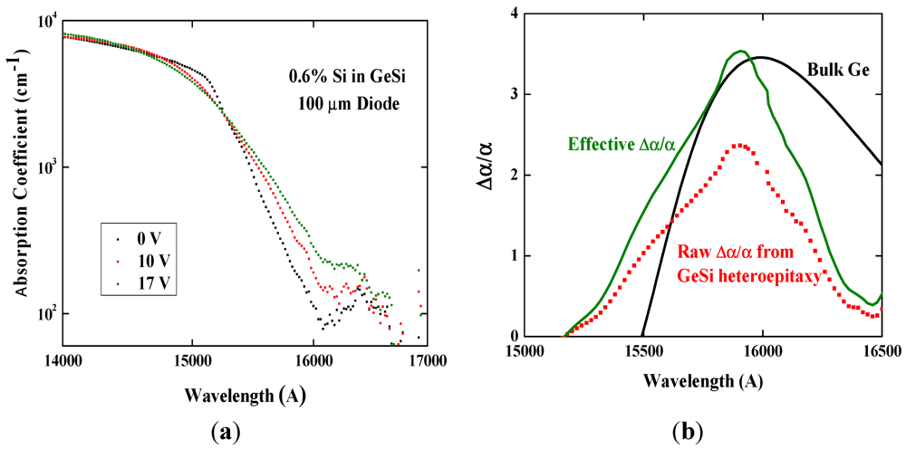
Recently, strong electro-absorption characteristic has been experimentally verified in Group IV semiconductors utilizing the direct interband transitions in compressively strained Ge quantum wells (QWs) with SiGe barriers [
14,
15]. Measured absorption change is of the same order as that of the conventional III-V based QCSE, with maximum absorption contrast ∆α/α ~4 at 1,461 nm under ~16 V/µm field. By employing wider GeSi wells (smaller quantum size energy up-shifts) and red-shifting the absorption edge at elevated temperatures, the absorption modulation band was extended out to 1,550 nm. However more work is still required to achieve strong absorption modulation for C band operation at room temperature.
Very recently, the same group at Stanford demonstrated room temperature operation with selective epitaxial growth of Ge/SiGe quantum wells [
16]. With SiO
2 mask patterned along the <110> direction, high quality epi layers with minimal inhomogeneous broadening was obtained. Thus a large E field up to 20 V/µm could be applied to align the absorption edge near 1550 nm. However, this high driving voltage may not be suitable for practical use with low-voltage CMOS technology. Other approaches such as adjusting the QW material to GeSn alloy [
17], are under investigation to lower the bandgap and bring the EA effect to 1550 nm.
Apart from the operating wavelength, the background absorption from the buffer layer may ultimately limit the contrast ratio for this type of modulator when operating in surface-normal or side entry geometries. While customized waveguide versions of this modulator can potentially mitigate the problem, the integration of the QCSE electro-absorption modulator (EAM) with the silicon waveguide is also a challenging task that is the subject of continuing research efforts.
On the other hand, the MIT group demonstrated the first waveguide integrated Franz-Keldysh-type electro-absorption modulator based on the direct transition in bulk tensile strained epitaxial GeSi [
18,
19,
20]. Processed with 180 nm CMOS technology, these integrated GeSi EAMs show >10 dB extinction ratio, ultra low power consumption (50 fJ/bit) and 14 nm wide operating wavelength range in the C band. This impressive FK effect obtained in bulk GeSi alloy implies that Ge on Si modulators are very promising candidates for the active Si-based photonics, and warrants more research on Ge FK designs focusing on large optical bandwidth and novel integration approaches. Recently, a butt-coupled Ge EA modulator fabricated on 3 µm SOI platform was reported. By carefully balancing the trade-offs between extinction ratio and insertion loss, the demonstrated device shows more than 30 GHz 3 dB bandwidth, with the ∆α/α value between 2.2–3.2 at 7.5 V/µm in the wavelength range 1,610–1,640 [
21,
22]. An evanescent-coupled Ge FK modulator [
23], targeted at more friendly integration into the mainstream CMOS node, was also reported. By designing a Ge rib on top of the Si slab, the optical signal is evanescently-coupled into the Ge active region via a crystalline silicon waveguide. An energy consumption of less than 100 fJ/bit is achieved under 7.5 V/µm field. The measured extinction ratio is larger than 10 dB over the wavelength range of 1,580–1,610 nm. However, this structure suffered from high insertion loss, which requires substantial waveguide design optimization to lower the coupling loss between Ge waveguide and Si waveguide. A brief review of FK EA device performance is provided in
Table 1 which also delineates the progress from early devices to the most recent ones.
Table 1.
Comparison of published Franz-Keldysh (FK) modulator performance.
Table 1.
Comparison of published Franz-Keldysh (FK) modulator performance.
| | SOI | Operating range (nm) | Footprint (μm2) | Speed (GHz) | Driving Voltage (V) | Δα/α |
|---|
| MIT [18,19,20] | - | 1,539–1,553 | 30 | 1.2 | 7 | ~2 |
| A*STAR [23] | 220 nm | 1,593–1,610 | 16 | 1.25 | 5 | >1 |
| Kotura/Oracle [21,22] | 3 μm | 1,610–1,640 | 45 | >30 | 4 | 2.2–3.2 |
As shown from this table, very different levels of performance for Ge FK modulator have been reported in the literature, and evidently Δα/α in the last column appears to be a good metric to illustrate this wide variance. A second observation in
Table 1 is that Δα/α has not reached the same performance level as that is found in bulk Ge [
13]. It therefore remains to be demonstrated that Ge FK modulators, when heteroepitaxial grown on Si, can ultimately reach the same device quality. In fact, the quality of epi may be part of the reason behind much of this phenomenon. Other factors may also contribute to the reported variation, such as: integration of GeSi into SOI waveguides, the SAG epi dependence and the impurity background levels during CVD growth.
To achieve system-ready optoelectronic performance in integrated Ge modulators, it is evident that a high quality Ge/GeSi epitaxial growth compatible with CMOS processes is the key to succeed. Germanium, as a bulk crystal, has a sharp absorption edge with a strong coefficient at the direct band gap. Unfortunately, when integrated onto SOI substrate, or when alloyed with dilute Si for blue-shifting to C-band operation, this strong Franz-Keldysh (FK) effect in bulk Ge is normally expected to degrade [
18]. In this paper, we report experimental study of selective growth of GeSi bulk epi by reduced pressure chemical vapor deposition. We first present a new epi growth module that can improve the resulting crystal quality and may improve the Δα/α metric. Secondly, we identify an unintentional oxygen impurity problem that can degrade Δα/α. Furthermore, we are the first to make a direct comparison of FK GeSi grown on SOI to the performance measured in bulk Ge, and we explicitly demonstrate that our GeSi FK devices do reach a quality nearly comparable to bulk Ge. Optical modulation up to 40 GHz is observed in waveguide devices. Herein we report comprehensive measurements and analysis of small signal characteristics for Ge FK devices for the first time. While high speed modulation could be limited by parasitic, transit time or material properties, our small signal analysis indicates measured bandwidth is limited by device parasitics.
Also shown in
Table 1, GeSi modulators usually require high driving voltage to reach the high extinction ratio, which becomes a large constraint for telecommunication application. To be compatible with CMOS drivers, driving voltage below 2 V are usually required. Therefore besides the excellent material quality, we also need novel device structures to achieve low voltage modulation.
2. GeSi Heteroepitaxial Growth
2.1. Growth Challenges
Due to its unique band structure, Germanium has always been a very popular research area for active photonic devices particularly in the search for a direct gap Group IV semiconductor. Not only have Ge-on-Si based photodectors been extensively investigated in recent years, new applications, such as Ge light emitters [
24] and Ge lasers [
25] were also successfully demonstrated on the Si platform. Prior to these works, more than thirty years of effort has been devoted to the material science of GeSi in search for a direct gap, emissive device. Still today, the heterogeneous integration of Ge/GeSi material system on SOI platform is a continuing research challenge that we consider next.
First, the difference of lattice constant between elemental Ge and Si is more than 4%, which is considered very large in semiconductor heteroepitaxy, and will seriously degrade the layer quality. Below the critical thickness, the Ge layer will take the lattice constant of the underlying Si substrate, so one can grow defect-free compressively strained Ge epi on Si. This critical thickness has been found to be about 4–10 nm [
26], while for the application of active photonic devices, a uniform Ge layer thicker than 1 µm may be required. When the thickness of the Ge/GeSi epitaxial layer exceeds its critical thickness, subsequent layer-by-layer growth (2-D) becomes unfavorable, a transition to three-dimensional (3-D) islands growth mode develops, which is then accompanied by epi layer lattice relaxation along with high misfit dislocations density and accompanied by high surface roughness. As a by-product of misfit dislocation, a large number of threading dislocations are created which interact and penetrate through the epilayer resulting in dislocation densities of over 10
9/cm
2. This kind of dislocation network is very difficult to avoid during the device fabrication, and hence forms a very important limitation in device performance.
Secondly, the unstrained transition energy of bulk Ge 0.8 eV is actually slightly smaller than the energy of 1.55 μm light, which makes it highly absorptive at this wavelength. A small amount of Si is required to be added into Ge to raise the direct transition energy, creating a material with an absorption edge aligned for C-band operation. Unfortunately, due to the high lattice mismatch between Ge and Si, and the lack of information for Ge-rich GeSi growth, precise control of the Si content inside the GeSi alloy while maintaining similar epi quality to that of the bulk becomes a complicated task. Different from homoepitaxial blanket growth of silicon, GeSi growth system requires a relatively low temperature or low pressure to avoid simply autodoping Ge into the Si substrate. However under these growth conditions, the diffusion length and surface mobility of the two species are so different that it might lead to composition non-uniformity when silicon is added to the epi. Therefore, the growth rate and silicon concentration in the layer is strongly dependent on the reactor settings, such as the gas flow rates, partial pressures and substrate temperature. If any of these parameters are changed, then new calibrations are required to accurately predict the epi thickness and composition.
In addition, waveguide integration, which usually involves selective epitaxial growth (SEG) or selective area growth (SAG), has proven to be very challenging due to process complexity and severe temperature constraints. The Ge epi process usually takes place after completing all the rapid thermal annealing (RTA) activation of CMOS implants steps. To integrate the GeSi EAM with silicon waveguide, through either butt coupling or evanescent coupling, GeSi selective growth needs to be performed on a pre-processed SOI wafer with all the silicon waveguides or slabs etched and windows patterned for the intended epi. Surface topology, sidewall roughness, as well as the arrangement of the SiO2 hard mask, all these pre-epi conditions will dramatically affect the material quality for the re-growth, and in some cases may damage the electro-absorption coefficient of the alloys. In addition, the size and density of the patterned windows will change the thickness and composition of the SiGe alloys in ways that are currently unpredictable. These properties have been termed as “global and local loading” effects and are akin to those found during III-V epi. For accurate alignment of the GeSi WG devices for C-band operation there will be interdependences on the gas selectivity, surface diffusivity, activation energy for decomposition. The overall quality of the GeSi epi in a window may be optimized at a different set of reactor conditions from those found on blank wafers.
2.2. Modified Two-Step Growth
The first epitaxy of GeSi heterostructures was achieved using MBE, and now most of the commercially available epitaxial wafers for GeSi use chemical vapor deposition (CVD) systems of different types for growth. The main reason behind the dominance of CVD in research and industrial environments is the particulate density. Solid source MBE has the disadvantage that material is deposited on the walls of the growth chamber which over time can fall off and create particles, while CVD reactors can produce films with high uniformity and reproducibility required for high yield production. Moreover, CVD has a higher growth rate and improved uniformity across the wafer when compared to MBE.
Despite the challenges with heteroepitaxy of germanium on silicon, many novel techniques based on CVD systems have been introduced to grow high quality Ge layers for device application. Here, threading dislocation densities have been reduced to the range of ~10
7/cm
2. Among them are, the graded buffer layer with chemical mechanical polishing (CMP) approach [
27], the two step growth method [
28], and the rapid melting growth method [
29]. The two step low-temperature buffer layer growth is often employed due to no requirement for thick buffer layers, capability of growing thick epi layers, and compatibility with the back end of line (BEOL) CMOS processing.
In this approach, a very thin, pure germanium layer of 30–50 nm is first deposited directly on Si or SOI substrate. This buffer layer growth (SEED growth) is done at a low temperature of 300 °C–350 °C to keep the epi layer topologically flat and strain relaxed. Here, low temperature prevents surface migration of Ge and prevents the SEED nucleation from reaching its otherwise thermodynamic equilibrium shape of a 3-D hemispherical dot on Si. The thickness of the SEED layer is chosen so that the flattened Ge island just begins to coalesce with its adjacent neighbors to form a contiguous film across the Si surface. Since the low-temperature buffer layer prevents the three-dimensional nucleation of Ge and the SEED thickness is greater than the critical thickness, misfit and threading dislocation generation is activated and the SEED accommodates most of the lattice mismatch. Thick film growth is then performed at high temperature (typically 600 °C) and at a larger growth rate. Due to threading dislocation annihilation in this thick film, along with high temperature growth, a much higher quality of epi film is produced. This film is then annealed at an even higher temperature (~800 °C) to further reduce the threading dislocation density (TDD) to around 107/cm2 level.
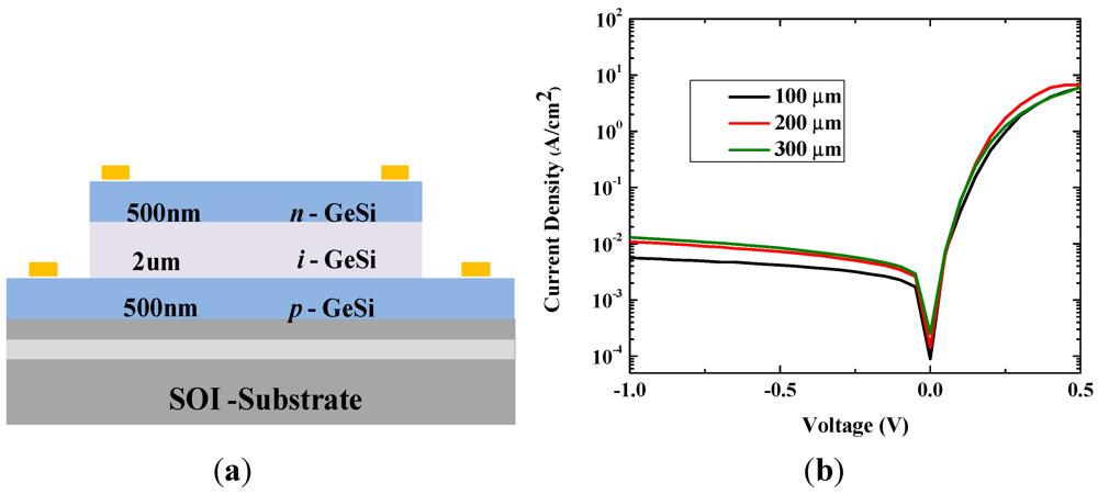
In this article, we investigate the selective epitaxial growth of the Ge-rich GeSi bulk epitaxial layers with a modified two-temperature technique. Growth was carried out in the reduced pressure CVD (RP-CVD) tool, with growth pressure ranging from 50 to100 Torr. After going through standard RCA clean and hydrogen baking, a thin GeSi buffer layer of ~100 nm was first deposited at 350–400 °C. Epitaxial GeSi layers with a total thickness of 3 µm in p-i-n geometry were then grown at a high temperature around 650 °C. A 2-µm thick intrinsic Ge1−xSix layer with various Si compositions was sandwiched between 0.5-µm thick p-type and 0.5-µm thick n-type regions.
The epi recipe used in this work differs from the standard two-step growth. Instead of conducting a post-growth annealing, a high temperature annealing step (750 °C for 10 min) was inserted between the two growths steps. As is known, annealing has always been an effective approach to reduce the threading dislocation density by expanding the misfit segment lengths. When deployed before the thick high temperature growth, a large amount of misfit dislocations can glide to the edge of the wafer (or SAG window), so that they do not generate new threading dislocations in the subsequent active epitaxial layers grown above the buffer. In addition, some threading dislocations can interact with each other during their motion, and thus lead to the so called “dislocation annihilation” inside the buffer layer. Therefore, the following thick growth is almost like a homoepitaxial growth on top of a fully relaxed and dislocation minimized buffer layer, and formation of new defects is highly discouraged. As shown in the following section, improved crystal quality with low defects and less surface undulation could be achieved with this buffer annealing method.
One of the most typically used source gases for Ge in CVD tools is germane (GeH
4). During the low temperature buffer growth, Ge will not grow on top of the native oxide with the GeH
4 source. However selective growth inside the oxide window with germane is more difficult during high temperature growth. Differential growth is more common in germane chemistries where single crystal material is grown in the device windows and poly- or amorphous- material is grown on top of the oxide mask. Moreover, due to its premature decomposition, germane is reported as a hazardous and toxic gas, which may further prevent its application in commercial technologies. Recently, a much safer alternative Ge source [
30] has been reported with a liquid organo germanium precursor—iso-butyl germane (IBGe). However, more studies are still required before this source gas can be used in a commercialized CMOS process. For our selective growth, a chloride based germanium source (GeCl
4) is used during the high-temperature deposition. Beside the nearly 100% growth selectivity over the device windows, this source gas also provides higher growth rate than that with germane, while still maintaining similar high crystal quality. However, for the buffer layer growth, due to the high thermal budget associated with GeCl
4, we still use germane as the source gas for germanium.
Today, in most of the top-tier CMOS foundries producing industrial grade electronics, germane is the preferred source gas for many of the reasons cited above. On the other hand GeCl4 has better selectivity in certain applications. However, there remain questions of residual contamination in the sources and no comprehensive comparison is readily known today. In a direct comparison of the two chemistries (GeH4 and GeCl4), we have measured the purity of both sources and found that the unintentional background to be in the low 1015 cm−3 level by Hall Effect measurement for each source epitaxy. A second, non-electrically active contaminant of bigger concern for the Ge heteroepitaxy problem is moisture, which has a direct impact on the optical quality of Germanium based devices, and will be addressed next.
2.3. From Surface Morphology to Oxygen Content
We characterize the surface roughness of the grown GeSi layers using atomic force microscopy (AFM). 10 µm by 10 µm AFM sweeps were used to exact the root-mean-square roughness (R
rms) to quantify the surface roughness.
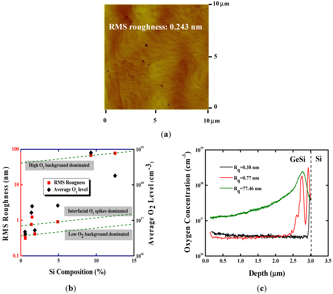
Figure 1(a) shows the typical result of an AFM image for GeSi epitaxial layers with low Si content (less than 2%). Clearly, these films all exhibited atomically flat surfaces with the very low R
rms ranging from 2 to 4 Å. Compared with the commonly reported surface roughness of ~1 nm for thick Ge films [
31] or GeSi alloys, our films demonstrates dramatic reduction in R
rms obtained with the buffer layer annealing technique.
However, the growth process of GeSi has been shown to be very sensitive to oxygen and other impurities, which may have significant impact on the surface roughness. Unlike the standard silicon CVD which is typically carried out at atmospheric pressure and involves the pyrolysis of the precursor gas at an elevated temperature (~1,000 °C), GeSi epitaxial growth processes are done at lower temperatures <800 °C to avoid the diffusion of the germanium and the development of surface undulations from high temperature growth. At these low growth temperatures, it is hard to volatilize the contaminating species completely with chamber baking, and hence the risk of oxygen incorporating into the wafer is higher. Basically, there are two main oxygen sources that will degrade the crystal surface morphology: interfacial O
2 and background O
2. Depending on the locations and background levels of oxygen inside the epitaxial layers, the GeSi heteroepitaxial growth conditions can be divided into three different regimes: epitaxy under a low O
2 background below 5 × 10
16 cm
−3 (preferred condition), degraded by interfacial O
2 contamination between the buffer layer and the substrate, and thirdly when dominated by high O
2 level (>5 × 10
17 cm
−3) in the growth chamber. As a results, measured R
rms can vary dramatically from below 5 Å to more than 70 nm, as shown in
Figure 1(b).
Figure 1.
(a) A typical AFM scan for GeSi alloy with 0.5% Si content; (b) RMS roughness and average oxygen level for GeSi alloys with various Si contents, revealing three different growth regimes associated with oxygen contamination; (c) SIMS profiles of the oxygen background for GeSi alloys grown under three regimes.
An oxide mask is usually employed for selective growth of GeSi. When Ge is deposited at a slow enough growth rate, Ge mesas only grow within the windows where the crystalline Si substrate is exposed. It has been proposed that is due to the reaction between the source gas and SiO
2 that forms volatile GeO and retards the nucleation of poly Ge on SiO
2. Indeed, it also been reported that GeH
4 actually etches the oxide at a slow rate [
32]. So if a native oxide is left on the surface of the Si wafer during the low temperature buffer growth, Ge will not grow until the native oxide is etched away. Unfortunately, SiO
2 mask is hydrophilic and it catches water drops after diluted HF dip before the growth. Even though the pre-growth baking completely evaporates these tiny water drops, some portion of oxygen will still be redeposited onto the substrate during the cooling down for buffer growth. As a result, this type of interfacial oxygen trapped between the buffer and substrate would form a thin layer of non-uniform native oxide, and thus induce a blurry, rough region during the buffer growth. From
Figure 1(b), one can find that a more than 2X surface roughing would be introduced by this type of oxygen contamination. To eliminate interfacial O
2, pre-growth procedures such as: spun dry, hydrogen bake, need to be carried out under optimized conditions to remove any residual native oxide. Extremely thin silicon trickle deposition has also been proved to be an effective way to dissolve oxygen attached to the surface.
As the growth temperature for CVD is reduced for GeSi alloys, lower background pressures are required to maintain an oxide free silicon surface to grow on. However, the background oxygen level sometimes is still very high, which is attributed to the memory effect in either the chamber or the mixture manifold. With these local oxides defects formed on the growth window, Stranski-Krastanov growth mode (3D) will develop after the initial two-dimensional wetting layer, leading to the formation of islands throughout the buffer layer and surface nucleation being exasperated after the high temperature growth. As indicated in
Figure 1(b), the heteroepitaxial growth under this condition will have serious surface undulation, and measured RMS roughness showed two orders of magnitude increase compared with those grown under low O
2 background. Installing purifiers at the source gas tanks to eliminate the oxygen contamination at lower furnace temperatures is a more prevalent fix to this problem. In addition, local contaminations-surface oxides attached to the growth chamber and gas inlets could also be eliminated by long pre-growth baking.
To establish the relationship between surface roughness and oxygen background, secondary ion mass spectrometry (SIMS) is employed to measure the oxygen background contamination. To obtain the accurate concentration of oxygen inside the films, silicon content is also profiled (not shown in the Figure) into the substrate for each GeSi films. Measured O
2 data are then normalized to the same substrate silicon concentration.
Figure 1(c) shows three typical SIMS profiles of GeSi alloys with different R
rms, representing the three different growth regimes associated with oxygen contamination. Epilayer with smooth surface (below 0.5 nm) shows very low O
2 background inside the epilayer ~3 × 10
16 cm
−3, with no sign of interfacial oxygen between buffer layer and substrate. For films with R
rms around 1–2 nm, large O
2 spikes at the GeSi/Si interface are observed in SIMS analysis, but measured background oxygen level is still below 5 × 10
16 cm
−3. When films are very rough, as expected, extremely high O
2 background in the order of 10
17 cm
−3 is detected.
In order to further quantify the oxygen impact on surface roughness, we use the average O
2 level, which is the average oxygen concentration over the entire alloy films, to cover both background and interfacial problems. As shown in
Figure 1(b), the calculated average oxygen contents inside each epilayers are in very good agreement with the measured RMS roughness of these films, indicating that the overall oxygen content inside the epitaxy, especially the residue background will greatly affect the surface roughness. For device applications, the residual background of oxygen needs to be reduced to the low 10
16 cm
−3 range.
Besides the strong impact from oxygen, growth undulations and surface roughening can be developed with increasing Si content in the GeSi films. Usually for Ge-rich GeSi alloys on silicon substrate, the presence of Si might alleviate the 3-D islanding problems by lowering strain energy. But on the other hand, Si content will also induce step bunching during Ge heteroepitaxy on Si and thereby add RMS roughness over pure Ge epitaxy.
Figure 1(b) shows the measured R
rms of GeSi alloys with different Si content under various growth conditions. As the dashed lines indicate, our experimental data suggests that higher Si concentration will lead to rougher surface under all of the three growth conditions regimes, revealing that step bunching may be the dominant factor controlling observed surface morphology. Fortunately, this characteristic roughness behavior for GeSi alloys does not show too strong Si content dependency. Smooth and flat films with less than 1 nm R
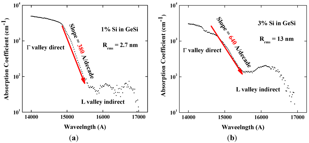
rms can still be obtained for alloys with up to 15% Si inside. Additionally, for GeSi to work in C band, only a small portion of Si is needed to form the alloys. Though the actual Si content may vary due to different film strain, the optimum Si composition ranges from 0.6% to ~1% for operation at 1,550 nm, suggesting that the high quality epi with roughness below 0.5 nm could be obtained for device application.
Finally we note that moisture and oxygen contamination in the supply source cylinders (GeH4, GeCl4) is a major problem during SiGe heteroepitaxy. Placement of purifiers to remove moisture from the source gas, and the geometry of the gas manifolds prior to introduction into the reactor, are all important considerations to mitigate oxygen incorporation and minimize RMS roughness. In our particular reactor configuration, we have configured the hardware so as to provide the lowest roughness. In our experiments, both germane and GeCl4 can produce similar smooth epi, while Germane based epi tends to produce slightly lower roughness than GeCl4, and this could be due to a lower residual oxygen level in the cylinders.
4. Waveguide Integrated Electro-absorption Modulator
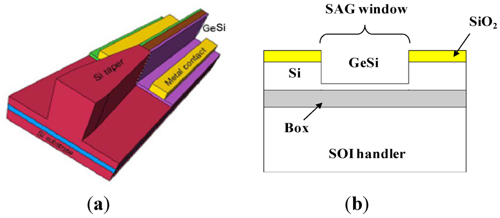
Waveguide integrated GeSi EA modulators are demonstrated with our modified two-step growth technique on the 3 µm SOI platform [
21,
22]. As shown in
Figure 5, the 2.7 µm thick GeSi layer is deposited into the deep-etched silicon trench via selective area growth (SAG). GeSi modulator waveguide is then formed with dry etch to butt couple with a deep-etched silicon waveguide. Finally, boron and phosphorous implantation is performed on the waveguide sidewalls to form a horizontally-oriented
p-i-n GeSi structure. The modulator waveguide width is designed to be 1 µm to avoid fabrication complexity. With an active length of 45 µm, the FK device demonstrated a strong electro-absorption effect over a wide spectral range: 1,610–1,640 nm. Under 4 V reverse bias, the measured extinction ratio ranges between 4.9 to 8.2 dB depending on wavelength, and the total transmission loss is in the range of 2.7–5.2 dB, which includes about 1.3 dB transition loss between Si and Ge waveguides.
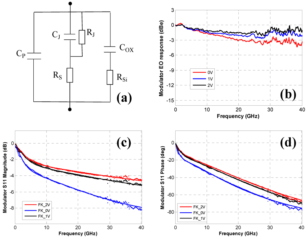
We studied the high speed behavior of the GeSi FK modulator, which includes curve-fitting of the measured S11 frequency response, and extracting the circuit values for the small signal circuit model.
Figure 6(a) is the circuit model for FK modulators built on SOI substrates. Here C
p is the capacitance between the electrodes sandwiched by the inter-layer dielectrics, R
si and C
ox denote to the substrate resistance and capacitance due to the buried oxide layer. C
j, R
j, and R
s are parameters to model the current path of the reversed biased
p-i-n junction. Optical modulators are electrically equivalent to a one-port device. This "one port" is across the top and bottom pins of
Figure 6(a). When testing modulator frequency response (
Figure 6(b)), we treat its modulated optical output as the second port. This method is commonly used for characterizing optical modulators. Optical reflections are not considered, and hence no S22 parameters are necessary.
Figure 5.
(a) Schematic of GeSi electro-absorption (EA) modulator integrated on 3 µm SOI platforms; (b) Schematic of the cross-section view of the selective area growth (SAG) of GeSi alloys.
Figure 5.
(a) Schematic of GeSi electro-absorption (EA) modulator integrated on 3 µm SOI platforms; (b) Schematic of the cross-section view of the selective area growth (SAG) of GeSi alloys.
Figure 6.
(a) Small-signal circuit model; (b) Measured electrical to optical (EO) frequency response of FK modulator; (c) Measured S11 magnitude with curve-fitting using the circuit model in (a); (d) Measured S11 phase with curve-fitting using the circuit model in (a).
Figure 6.
(a) Small-signal circuit model; (b) Measured electrical to optical (EO) frequency response of FK modulator; (c) Measured S11 magnitude with curve-fitting using the circuit model in (a); (d) Measured S11 phase with curve-fitting using the circuit model in (a).
We performed curve fitting to S11 to extract the circuit parameters. As shown in
Figure 6(c,d), excellent curve fittings (solid lines) are achieved for both the phase and magnitude of measured S11 (dotted lines) at all the voltages. Extracted circuits values are presented in
Table 2. The junction capacitance decreases with the bias because the junction depletion width increases with the bias. C
ox and R
si in principle should not change much with bias, and the observed variation is mostly due to numerical error associated with the extracted circuit values. Note that the effect of C
ox and R
si on the measured S11 is small. The purpose of extracting circuit values is to provide a semi-quantitative guideline to our modulator driver design and to help us understand the modulator behavior. Both these purposes are served in spite of small variations in the extracted model. Using these circuit values, we can predict, to some extent, the modulator frequency response. It is close to but not exactly the same as in
Figure 6(b), since there are some other effects (carrier screening due to photocurrent, carrier transit time,
etc.) that may modify the frequency response. As shown in
Figure 6(c,d), the fitting works well up to 40 GHz.
Table 2.
Extracted circuit values under different reverse bias.
Table 2.
Extracted circuit values under different reverse bias.
| | Cp (fF) | Rs (Ω) | Cj (fF) | Rj (Ω) | Cox (fF) | Rsi (Ω) |
|---|
| 0 V | 15.6 | 66.1 | 66.6 | 1,663 | 237 | 249 |
| 1 V | 17.7 | 58.6 | 43.3 | 1,750 | 135.5 | 317 |
| 2 V | 20.7 | 66.9 | 36.9 | 1,970 | 125.9 | 341 |
Electrical to optical (EO) frequency response of the fabricated device was tested to further evaluate the high speed performance.
Figure 6(b) shows the measured EO response of the modulator under various reverse biases. Clearly this waveguide integrated FK modulator has a more than 40 GHz 3 dB bandwidth with bias voltage of 2 V. The bandwidth increases with bias due to reduced junction capacitance. An interesting part in the circuit model is the C
ox and R
si branch. The low R
si value in
Table 2 suggests that there is a significant current flowing through this branch at high frequency, which reduces the RC-limited bandwidth and increases the modulator power consumption. This can be fixed by using a high resistive SOI substrate handler.
The data rate dependence on the heat management for an FK versus alternative modulators is an extremely important subject. There are several device factors to consider, such as the frequency dependence of the junction capacitance, photocurrent and leakage current just to mention a few. To do adequate justice and consider all the complex issues that interplay requires a comprehensive treatment of the device, the link, its thermal environment and its packaging. Such an analysis goes beyond the scope of our manuscript but is clearly a topic warranting future attention.


