High-Q MEMS Resonators for Laser Beam Scanning Displays

Fraunhofer Institute for Silicon Technology ISIT, Fraunhofer Strasse 1, Itzehoe D-25524, Germany
*
Author to whom correspondence should be addressed.
Micromachines 2012, 3(2), 509-528; https://doi.org/10.3390/mi3020509
Submission received: 13 April 2012
/
Revised: 5 May 2012
/
Accepted: 31 May 2012
/
Published: 6 June 2012
(This article belongs to the Special Issue Micromachined High Frequency Acoustic Wave Resonators and Filters)
Abstract
:This paper reports on design, fabrication and characterization of high-Q MEMS resonators to be used in optical applications like laser displays and LIDAR range sensors. Stacked vertical comb drives for electrostatic actuation of single-axis scanners and biaxial MEMS mirrors were realized in a dual layer polysilicon SOI process. High Q-factors up to 145,000 have been achieved applying wafer level vacuum packaging technology including deposition of titanium thin film getters. The effective reduction of gas damping allows the MEMS actuator to achieve large amplitudes at high oscillation frequencies while driving voltage and power consumption can be minimized. Exemplarily shown is a micro scanner that achieves a total optical scan angle of 86 degrees at a resonant frequency of 30.8 kHz, which fulfills the requirements for HD720 resolution. Furthermore, results of a new wafer based glass-forming technology for fabrication of three dimensionally shaped glass lids with tilted optical windows are presented.
1. Introduction
The capability to deflect a laser beam at high speed has let resonating MEMS mirrors become attractive for imaging applications [1] and for application in laser projection displays [2,3] early on. MEMS scanning mirror based projection displays represent an elegant solution to overcome the limitation of insufficient screen size of portable electronic devices like mobile phones, digital cameras or media players. Either small enough to be incorporated directly into these portable devices or used as an accessory module, MEMS scanning mirror based projection displays may offer screen sizes several times larger then the portable devices themselves. Besides use in consumer products, miniature laser scanning projection displays are also of particular interest for automotive head up displays and dashboard displays.
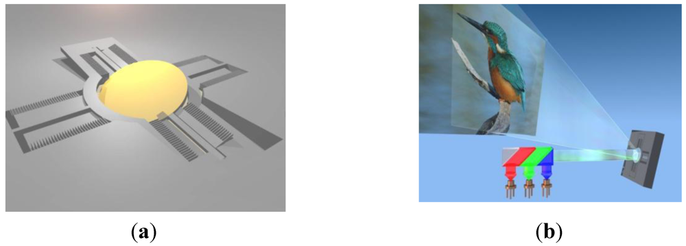
A MEMS scanning mirror consists of a silicon mirror plate which is movably suspended by lateral torsional flexures. In a laser projection display the laser beam needs to be scanned in two perpendicular axes. The two scan axes can be implemented either by two separate single axis mirror chips or on a single silicon chip using a gimbal mount configuration (Figure 1(a)). The inner fast axis of such a biaxial scanner performs the horizontal line scan while the outer gimbal axis performs the slow vertical deflection. The divergent output beams of a red, green and blue laser first are collimated by lenses and then are combined to a single laser beam that is directed on the biaxial scanning mirror. The MEMS mirror scans the laser beam in two axes across the projection screen (Figure 1(b)). Accurate control of the laser output synchronized to the biaxial MEMS mirror movement enables to project full color images pixel by pixel. In contrast to modulator matrix based projectors using DLP or LCOS such scanning laser beam projectors do not need any focusing optics since the projected image is always in focus at any distance.
Figure 1.
(a) Gimbal mounted biaxial MEMS scanning mirror electrostatically actuated by stacked vertical comb drives; (b) Biaxial MEMS scanning mirror in a laser projection display.
Figure 1.
(a) Gimbal mounted biaxial MEMS scanning mirror electrostatically actuated by stacked vertical comb drives; (b) Biaxial MEMS scanning mirror in a laser projection display.

To meet the high-resolution requirements of modern displays, which is HD720 or higher, the MEMS mirror needs to oscillate at a frequency of at least 27 kHz, enabling the projection of 54,000 lines per second. A resolution of HD1080 requires even higher oscillation frequencies up to 54 kHz depending on the chosen scanning concept (Table 1).

| WVGA | HD720 | XGA | HD1080 | |
|---|---|---|---|---|
| pixel resolution | 852 × 480 | 1,280 × 720 | 1,024 × 768 | 1,920 × 1,080 |
| corresponding line scan frequency @ 60 Hz image refresh [lines/second] | 28,800 | 43,200 | 46,080 | 64,800 |
| required MEMS oscillation frequency raster scan mode @ 80% duty cycle [kHz] | 18 | 27 | 28.8 | 40.5 |
| required MEMS oscillation frequency raster scan mode @ 60% duty cycle [kHz] | 24 | 36 | 38.4 | 54 |
| required MEMS oscillation frequency Lissajous scan mode [kHz] | 22.6 | 33.9 | 36.2 | 50.9 |
There are two principally different scanning and projection concepts: Raster scanning based projection and Lissajous scanning based projection. In a raster-scanning concept, the fast axis of the MEMS mirror oscillates at resonance while the slow axis usually performs a non-resonant scan with a saw tooth characteristic. Defining duty cycle as ratio of linear rise time of the saw tooth function and its retrace time, it is desirable to achieve a duty cycle as high as possible since it corresponds to the lowest fast axis frequency requirement. Reversely saying, a low duty cycle corresponds to a high frequency requirement for the fast axis since the total line number has to be projected within a shorter time. Besides meeting the frequency requirements of the fast axis it is extremely challenging to design and manufacture a slow axis MEMS mirror capable of performing a saw tooth like scan at high duty cycle, low linearity-error and at a sufficiently large tilt angle [4].
In a Lissajous projector both axes of the biaxial MEMS scanning mirror, or alternatively, both axes of two single axis MEMS scanning mirrors are driven at resonance or close to resonance. On the one hand, resonant actuation facilitates the achievement of the required scan angles of the slow axis but on the other hand, it also increases the frequency requirement of the fast axis (Table 1).
Regardless of what concept is chosen, to meet the relevant display resolution requirements the MEMS scanning system needs to achieve very large deflection angles. The number of pixels N resolved by a scanned beam laser display is proportional to the total optical scan angle θopt (which is equal to four times the mechanical tilt angle amplitude θmech) and inversely proportional to the spot size on the projection screen. The minimum spot size is inversely proportional to the laser beam diameter and therefore limited by the mirror diameter D.
 (1)
(1) Therefore, the characteristic number to indicate the MEMS mirror’s achievable resolution is the so-called “theta-D-product”, defined as the product of mechanical tilt angle amplitude θmech and mirror diameter D. The theta-D-products required for different display formats are listed in Table 2 [5].
Table 2.
MEMS oscillation amplitude requirements in a laser projection display [5].
| WVGA | HD720 | XGA | HD1080 | |
|---|---|---|---|---|
| pixel resolution | 852 × 480 | 1,280 × 720 | 1,024 × 768 | 1,920 × 1,080 |
| required theta-D-product [degrees*mm] | +/−10 | +/−15 | +/−12 | +/−22.5 |
2. MEMS Mirror Concept
It is the focus of this paper to present a MEMS mirror concept and a corresponding fabrication technology that enable the fulfillment of the already presented high-resolution display demands.
The achievable optical resolution is always limited by the strength of damping that the MEMS mirror experiences. At atmospheric pressure, damping by gas molecules predominates over intrinsic damping mechanisms. It so far has been tried to shift the resolution limits only by increasing the driving power in order to increase the torque acting on the MEMS mirror axes. Consequently, driving circuits for electrostatically actuated MEMS mirrors have to handle disadvantageously high driving voltages [6,7] or, in the case of electromagnetically actuated mirrors, driving currents and power consumption are disadvantageously high [4].
Thus, the MEMS mirror concept proposed in this paper is to reduce gas damping instead of further increasing power consumption. Reduction of damping effectively can be achieved by vacuum encapsulation of resonantly actuated MEMS mirrors. Since vacuum packaging on chip level is too expensive and time consuming, it is part of the concept to establish a wafer level vacuum packaging technology. Electrostatic actuation based on stacked vertical comb drives as depicted in Figure 2, is the chosen driving concept, because it is fully compatible with hermetic wafer level vacuum encapsulation. It is compatible with high temperature wafer bonding processes because it does not require the use of additional materials of non-matching expansion coefficients as for example thick metal layers for high density planar coils of electromagnetic drives.
Figure 2.
Electrostatic actuation by stacked vertical comb drives.

Vacuum encapsulation of resonant MEMS scanning mirrors is a technology that can be used beneficially in raster scanning displays as well as in Lissajous scanning laser displays. In a Lissajous approach both resonant mirror axes can benefit from damping reduction. Lissajous displays can either be configured as serial arrangement of two single-axis vacuum packaged scanning mirrors or in a single chip solution by choosing a vacuum packaged biaxial gimbal mounted design.
However, in a raster scanning MEMS concept, the reduction of damping is disadvantageous for the non-resonant slow axis because it is difficult to suppress overshoot caused by parasitic resonance excitation. Therefore, the optimum setup of a raster scanning system applies a vacuum packaged fast axis scanning mirror and a slow axis MEMS mirror working at atmospheric pressure.
3. MEMS Mirror Fabrication Process
The MEMS scanning mirrors are fabricated on n-doped 8-inch silicon substrates of 725 µm thickness. One of the key-features in the fabrication process is the deposition of thick polysilicon layers in an epitaxial reactor using SiH2Cl2 (Dichlorosilane) as a precursor [8]. That polysilicon deposition process running at 1,080 °C in a reduced pressure regime achieves a high deposition rate of 1.4 µm per minute and provides polysilicon device layers of extremely low stress (<10 MPa).
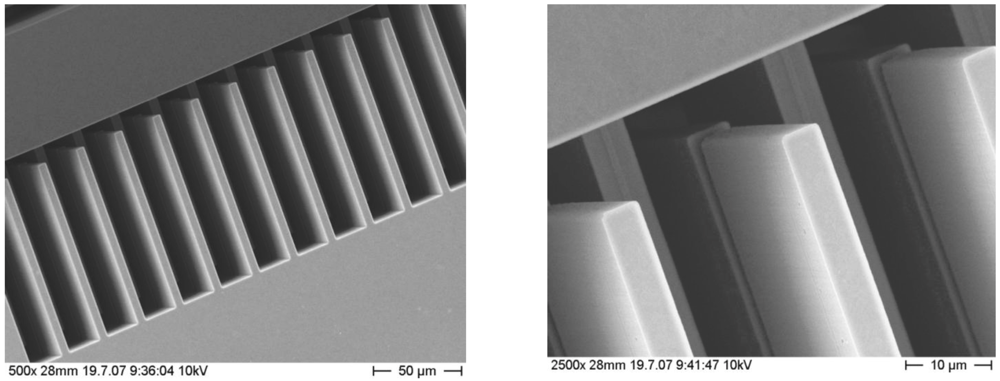
The MEMS mirror fabrication process starts with thermal growing of a 1 µm thick silicon oxide layer (Figure 3(a)). A 190 nm thick LPCVD polysilicon layer is deposited serving as a seed layer for the following deposition of a 35 µm thick polysilicon device layer. To reduce the roughness and topography the device layer is polished in a CMP process to a final thickness of 30 µm (Figure 3(b)). Next, a first 1.2 µm thick silicon oxide layer is deposited in form of a LPCVD-TEOS deposition. Another 500 nm thick polysilicon layer is deposited in a LPCVD-process. Photolithography followed by dry etching produces the wires of an electrical interconnect layer (Figure 3(c)). A second silicon oxide layer is again deposited in form of a LPCVD-TEOS deposition. Photolithography and plasma etching are applied in order to produce a buried oxide hard mask which is used in a later dry etch of the device layer. But that process step is also used to open local contacts to the polysilicon interconnect layer (Figure 3(d)). A second 30 µm thick polysilicon device layer is produced in the same sequence that was applied for forming the first device layer (Figure 3(e)). In the next process block metallization of mirror and contact pads is done. It includes deposition of a titanium-silver stack by evaporation followed by sputter deposition of a thin aluminum-nitride layer which is used to protect the silver mirror coating. Electroplating is applied to deposit 1 µm of gold in the lithographically opened photoresist areas to form the contact pads (Figure 3(f)). In a single deep reactive ion etching step that uses the combination of a photoresist mask and the buried oxide hard mask both device layers are patterned (Figure 3(g)). A further DRIE process is applied to etch deep grooves to the reverse side of the MEMS mirror wafer. The plasma etching step automatically stops when the thermally grown initial oxide layer is reached. After HF-vapor etching the MEMS mirror is finally released (Figure 3(h)). Fabricated stacked vertical comb drives are shown in Figure 4. The electrode finger width is 6 µm and 5 µm for the lower polysilicon layer and the upper polysilicon layer, respectively. The electrode gap between the lower polysilicon electrode fingers is 6 µm.
Figure 3.
MEMS mirror fabrication process.

Figure 4.
SEM pictures of stacked vertical comb drives fabricated in the dual layer polysilicon SOI process.
Figure 4.
SEM pictures of stacked vertical comb drives fabricated in the dual layer polysilicon SOI process.

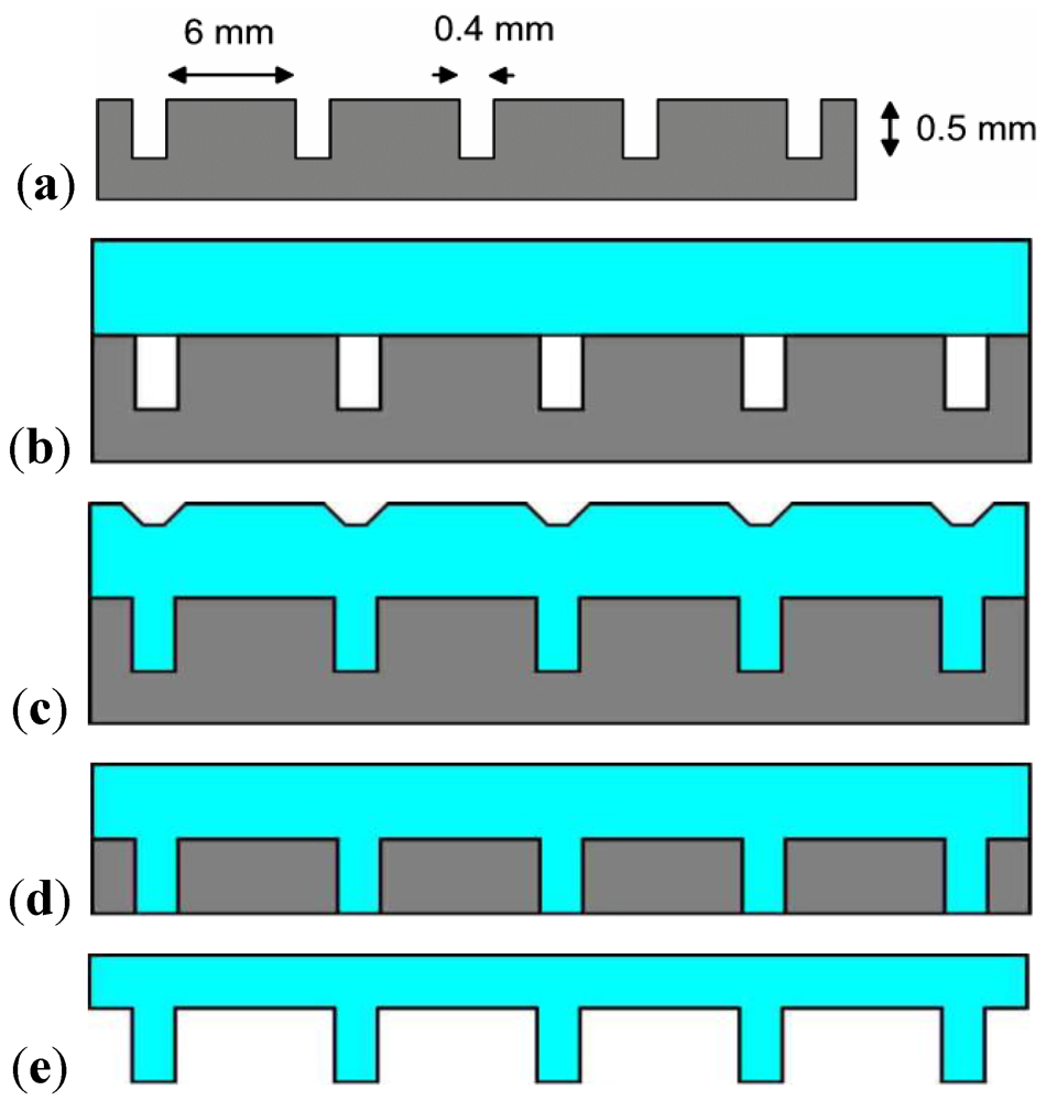
4. Fabrication of Glass Cap Wafers
The design of a packaged MEMS scanning mirror has to consider a sufficiently large space between mirror plate and transparent glass lid. Therefore, the design of a suitable glass cap wafer has to include deep cavities and windows of high optical quality. To enable low cost mass production of such glass cap wafers, a glass forming technology has been developed that uses a structured silicon wafer as a mold in a high temperature glass reflow process [9,10]. In the first step, several hundred microns deep trenches are etched into the surface of a polished silicon wafer (Figure 5(a)). Then a borosilicate glass wafer is anodically bonded to the structured silicon wafer under vacuum (Figure 5(b)). Next, the wafer compound is heated up to temperatures above 600 °C. The glass wafer gets soft and flows into the silicon mold (Figure 5(c)). After a cooling period, the glass surface shows high topography. To achieve a plane surface of low roughness again, the glass surface is polished. In addition, the silicon part is also grinded and polished until a smooth planar silicon surface with embedded glass frames becomes visible (Figure 5(d)). In the final step, the silicon mold is removed by wet-chemical etching in TMAH (Figure 5(e)).
Figure 5.
Fabrication of glass cap wafers.

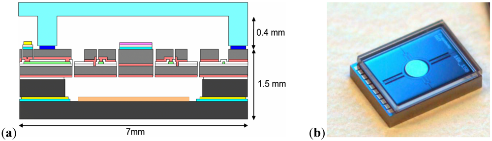
5. Wafer Level Vacuum Packaging Process
In the first step of the wafer level vacuum packaging process, the formed glass wafer with deep cavities and windows is bonded to the MEMS wafer applying a glass frit bonding process at around 400 ° C. In the second step, a silicon wafer is coated with a titanium/gold layer serving as a plating base for subsequent electroplating of a 3 µm thick layer of gold. On that layer of gold, another 400 nm thick titanium layer is deposited and patterned. It later serves as a thin film getter. This coated and patterned base wafer is eutectically bonded to the reverse side of the MEMS wafer at a temperature of 363 °C (Figure 6(a)). The titanium getter chemically binds gas molecules and thereby reduces the pressure inside the hermetically sealed microactuator cavity to around 0.1 Pa.
Figure 6.
(a) Schematic cross section of a wafer level vacuum packaged MEMS mirror with integrated thin film getter; (b) Vacuum packaged biaxial MEMS mirror.
Figure 6.
(a) Schematic cross section of a wafer level vacuum packaged MEMS mirror with integrated thin film getter; (b) Vacuum packaged biaxial MEMS mirror.

6. Characterization of Vacuum Packaged Resonant MEMS Scanning Mirrors
In this section, the characteristic behavior of different vacuum packaged resonant 1D- and 2D-MEMS scanning mirrors is presented.
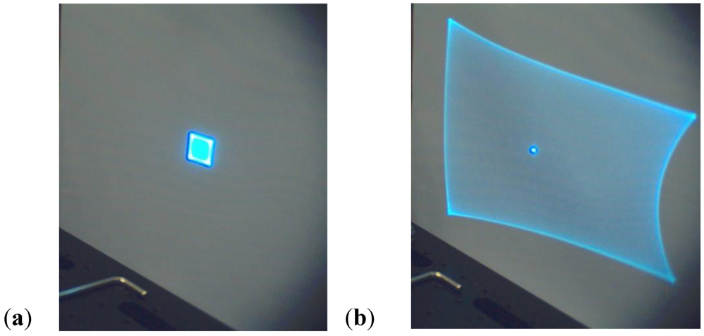
6.1. Qualitative Result
Prior to a detailed presentation of measurement data, a simple qualitative result shall be presented in order to give an impression of the benefit of vacuum encapsulated MEMS mirrors. As Figure 7 shows, the oscillation amplitude of the biaxial vacuum packaged MEMS scanning mirror is roughly 10 times larger in each axis than a MEMS mirror of identical design actuated at atmosphere. The bright spot in the center of the projection area is produced by direct reflection of the incoming laser beam at the glass cover of the vacuum packaged mirror.
Figure 7.
(a) Biaxially scanned laser beam based on a MEMS mirror actuated at atmosphere with 40 V applied to fast axis (17.8 kHz), 5 V applied to slow axis (0.5 kHz); (b) Biaxially scanned laser beam based on identical but vacuum packaged MEMS mirror design at identical driving voltages of 40 V applied to fast axis, 5 V applied to slow axis.

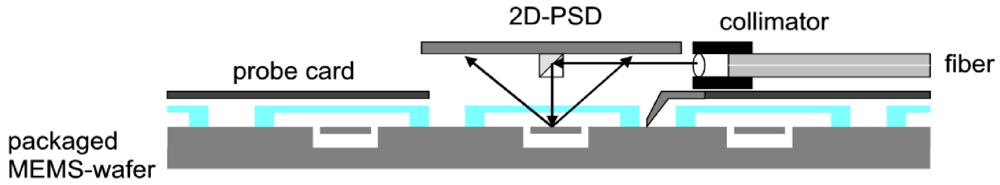
6.2. Measurement Setup for Wafer Level Testing of Vacuum Packaged MEMS Mirrors
A cap dicing process, in which only the glass cap is diced along the rows of contact pads, is done before wafer level testing begins (Figure 6). Wafer level testing is performed using a specially configured probe station (Figure 8). A grin lens collimates the divergent beam of a fiber coupled laser diode before a tiny beam splitter cube is used to reflect and redirect the collimated laser beam in such a way that the laser beam impinges perpendicularly on the MEMS mirror. Contacted by the probe pins of the probe station the MEMS mirror is electrostatically actuated in one or two axes and thus deflects the laser beam which finally hits a large two-dimensional position sensitive detector (2D-PSD). A signal processing electronics is used that directly translates the position dependent photocurrent into an xy-position, which allows measuring the mirror’s oscillation angle amplitude. The oscillation angle amplitude equals one-fourth of the measured total optical scan angle.
Figure 8.
Schematic of the optical measurement setup used for wafer level testing.

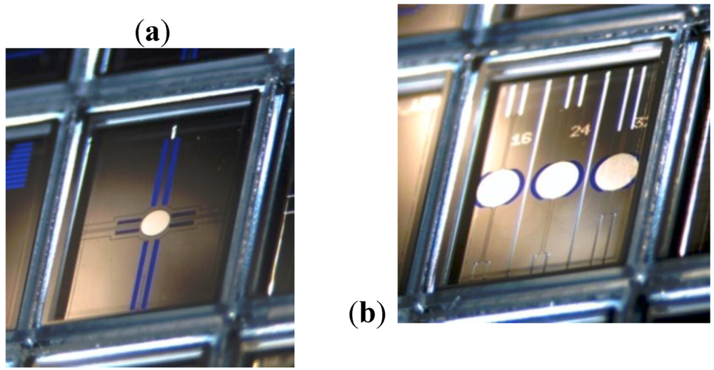
6.3. Characterization of 1D-Fast Axis Scanners
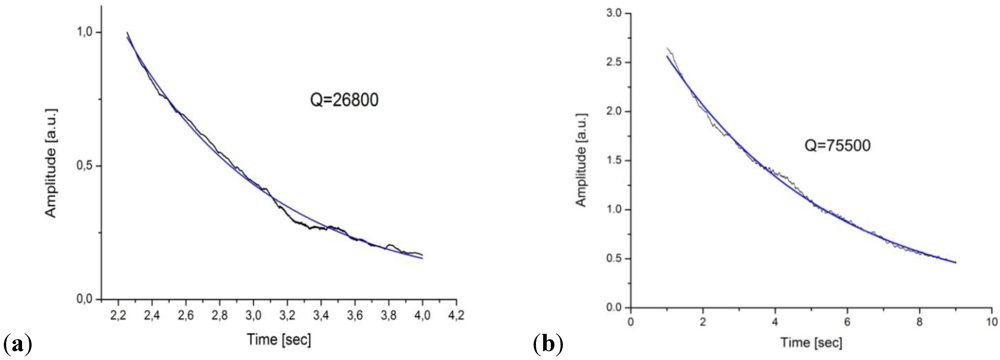
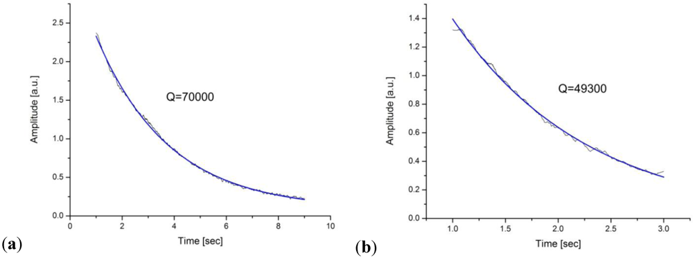
In this section measurement data of different vacuum encapsulated fast-axis MEMS mirror resonator designs is presented. Pictures of the two chips incorporating four different MEMS mirrors are shown in Figure 9. Table 3 provides the related dimensions of mirror geometry and torsional suspensions. The four MEMS mirrors exhibit resonant frequencies between 16 kHz and 38 kHz. For each of these MEMS scanners the decay of the resonance amplitude was recorded after switching off the driving signal for determination of the MEMS scanner’s Q-factors.
Figure 9.
Single-axis high-Q resonators. (a) Design #1 (b) Designs #2, #3, #4.

Table 3.
Geometrical design data and measurement data of four different fast axis mirror resonators.
| Design #1 | Design #2 | Design #3 | Design #4 | |
|---|---|---|---|---|
| Mirror aperture size | 0.8 mm | 1.0 mm | 1.0 mm | 1.0 mm |
| Mirror thickness | 60 µm | 60 µm | 60 µm | 60 µm |
| Width of beams | 47 µm | 44 µm | 65 µm | 65 µm |
| Length of beams | 1,440 µm | 1,450 µm | 1,450 µm | 600 µm |
| Thickness of beams | 60 µm | 60 µm | 60 µm | 60 µm |
| Resonant frequency | 30.8 kHz | 16.5 kHz | 25.1 kHz | 38.5 kHz |
| Q-factor | 26,800 | 75,500 | 70,000 | 49,300 |
| Theta-D-product | 17,3 mm × deg | 13.8 mm × deg | 13.8 mm × deg | 10.8 mm × deg |
Figure 10.
Resonance amplitude decay plots of different high-speed MEMS mirror resonators. (a) Design #1 (b) Design #2.
Figure 10.
Resonance amplitude decay plots of different high-speed MEMS mirror resonators. (a) Design #1 (b) Design #2.

Figure 11.
Resonance amplitude decay plots of (a) Design #3 (b) Design #4.

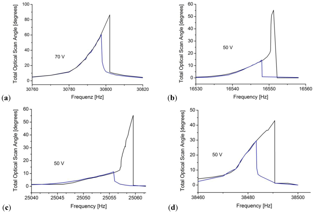
Figure 12.
Frequency response. Blue curves represent downward sweep, black curves represent upward sweep. (a) Design#1 (b) Design#2 (c) Design#3 (d) Design#4.
Figure 12.
Frequency response. Blue curves represent downward sweep, black curves represent upward sweep. (a) Design#1 (b) Design#2 (c) Design#3 (d) Design#4.

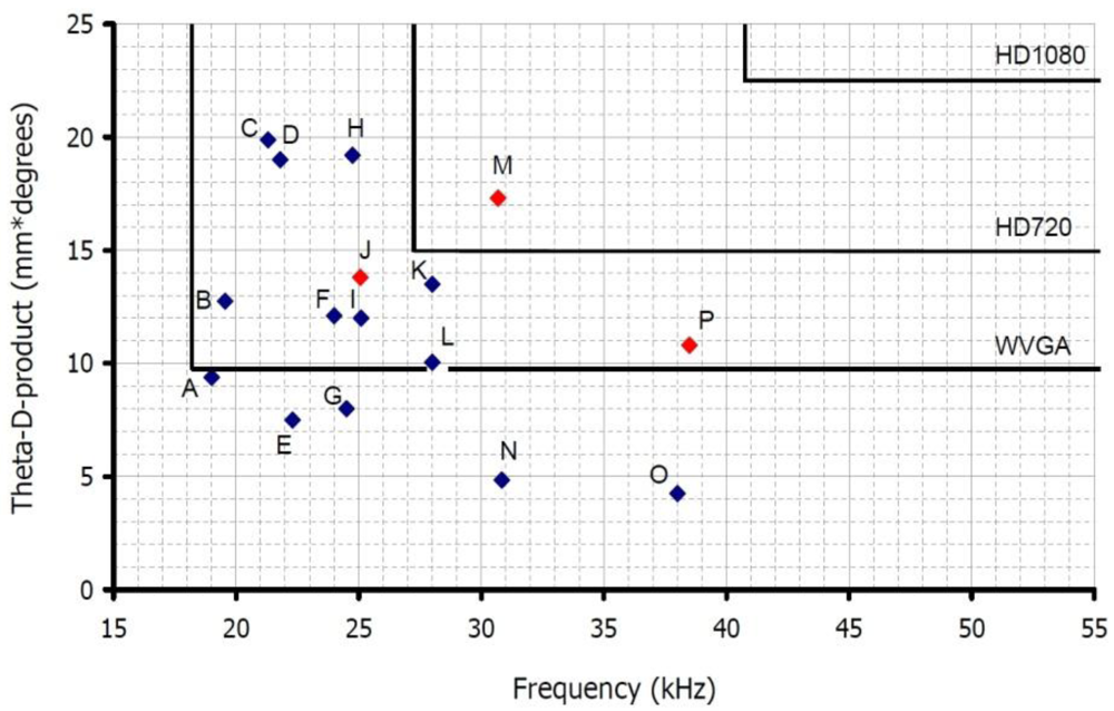
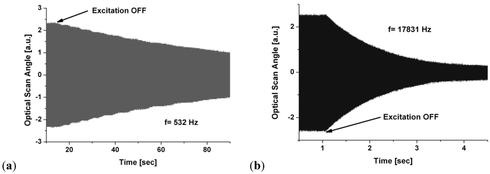
As Figure 10 and Figure 11 show, damping inside the MEMS package is so low that the high frequency scanning mirrors continue to oscillate for many seconds without excitation signal. For the three resonator designs #2, #3 and #4, which are implemented on a single chip, Q-values of 75,500, 70,000 and 49,300, were measured, respectively. The highest resonant frequency coincides with the lowest measured Q-value and vice versa. The corresponding frequency response plots of these four different MEMS scanners are shown in Figure 12, presenting nonlinear resonance characteristics. All scanners exhibit spring stiffening effects, making it necessary to drive the oscillators into resonance from lower frequencies to higher frequencies. However, designs #2 and #3 show a considerable lowering of that stiffening effect at total optical scan angles larger than 20 degrees, corresponding to mechanical tilt angle amplitudes larger than five degrees. Design #1 principally differs from the other three designs with respect to the comb electrode arrangement. In design #1 the electrodes are placed close to the torsional axis which enables overlap with the stator electrodes over a large angular range. The electrode fingers of the other three resonators are located along the mirror edges at a larger distance to the torsional axis, enabling only a short angular range of electrode finger overlap. Design #1 achieves a total optical scan angle of 86 degrees at 30.8 kHz. Because of a mirror aperture size of 0.8 mm the theta-D-product, which is the product of mirror size and mechanical tilt angle amplitude, is calculated to be 17.3 mm × degrees. That is sufficient for a raster-scanning display with HD720 resolution. A comparison of the fast axis MEMS scanning mirror presented in this work with other published developments is given in Figure 13.
Figure 13.
Comparison of fast axis MEMS scanning mirrors. The reference numbers of the corresponding published articles are listed in the caption below.
Figure 13.
Comparison of fast axis MEMS scanning mirrors. The reference numbers of the corresponding published articles are listed in the caption below.

| (A) = [11] | (B) = [12] | (C) = [13] | (D) = [14] | (E) = [15] | (F) = [16] | (G) = [17] | (H) = [18] |
| (I) = [19] | (J) = this work design #3 | (K) = [20] | (L) = [20] | (M) = this work design #1 | (N) = [21] | (O) = [22] | (P) = this work design #4 |
During oscillation a resonant MEMS scanning mirror does not remain perfectly flat. It always experiences dynamic deformation. Maximum deformation occurs in the turning points of the oscillation where the angular acceleration ![Micromachines 03 00509 i002]() is:
is:
 is:
is: (2)
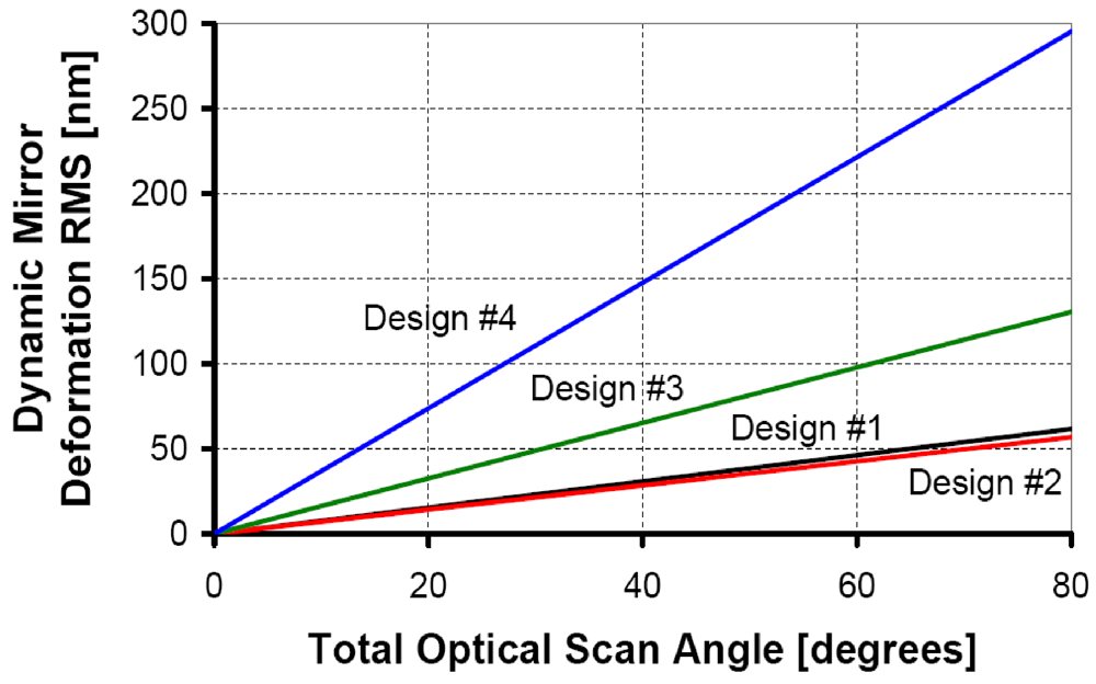
(2) where θ is the mirror tilt angle amplitude and ω is the angular frequency. Because mirror deformation contributes to beam divergence, it reduces the optical resolution of the projection display. It can be shown that the dynamic mirror deformation δ scales proportional to the fifth power of mirror size L [23]:
 (3)
(3) where f is the scan frequency, E is Young’s modulus and t denotes the mirror thickness. The dynamic mirror deformation that has to be expected for the four different single axis MEMS mirrors has been calculated by Finite Element Analysis applying the acceleration given by Equation (2). In order to minimize loss of resolution, dynamic deformation should not exceed one tenth of the wavelength. That means that the deformation should be less than 50 nm. In Figure 14, the calculated dynamic deformations are plotted as a function of the scan angle. For design #1 and design #2 the deformation is within the limits of lambda/10 up to a total optical scan angle of 65 degrees. For designs #3 and #4 the deformation increases much faster because of the mirror diameter and a higher scan frequency. Mirror flatness can be improved by either increasing the thickness of the mirror plate or by using a more sophisticated mirror mounting [24].
Figure 14.
Finite Element Analysis based calculation of dynamic mirror deformation for all four designs.
Figure 14.
Finite Element Analysis based calculation of dynamic mirror deformation for all four designs.

6.4. Characterization of a 2D-Gimbal Mounted Scanner
In this section a biaxial resonant gimbal mounted MEMS mirror for Lissajous laser projection is presented (Figure 15). The principal mirror properties are:
- Mirror aperture size: 1 mm
- Fast axis resonant frequency: 17.8 kHz
- Slow axis resonant frequency: 0.5 kHz
Figure 15.
Biaxial gimbal mounted MEMS scanning mirror for Lissajous laser projection.

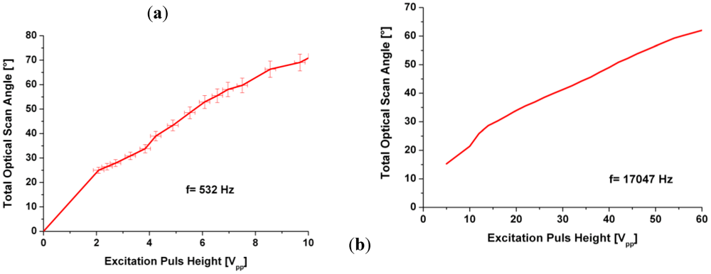
This MEMS scanner features separated pairs of driving and sensing comb electrodes for each axis. While driving electrodes are placed distant to the axis, the sensing electrodes for capacitive phase feedback are arranged close to the respective axis. Because of the very low gas damping, the vacuum packaged biaxial MEMS scanning mirror accumulates energy over several thousand oscillations. Figure 16 shows the slow decay of the resonance amplitude after switching off the excitation signal. It takes about 90 s until the resonance amplitude of the gimbal reduces by a factor of two. The Q-factors were calculated to be 145,000 and 60,000 for slow axis and fast axis, respectively. The benefit of this energy conserving MEMS scanner becomes obvious when analyzing the deflection angle as a function of voltage, shown in Figure 17. An excitation pulse height of only 10 V is necessary to drive the slow axis to a total optical scan angle of more than 70 degrees, whereas the fast axis needs a pulse height of only 60 V to achieve a total optical scan angle of 60 degrees. Due to the low driving voltages the power consumption of the 2D-scanning mirror is less than one milliwatt.
Figure 16.
Amplitude decay over time of gimbal (a) and mirror (b).

Figure 17.
Total optical scan angle as function of driving voltage for gimbal (a) and mirror (b).

6.5. Capacitive Phase Feedback and Closed Loop Control
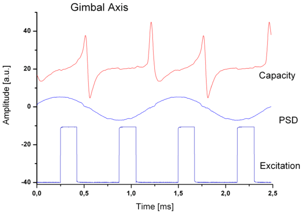
Because of the high Q-factors, the frequency response of the vacuum encapsulated 2D-MEMS scanning mirror exhibits extremely narrow resonance peaks and steep phase-frequency dependence. This leads to a high sensitivity of the oscillation amplitude to changes of temperature. Since in a laser video projection the changing laser power permanently causes temperature changes of the mirror and its suspensions, it is necessary to control each scan axis by an individual and independent phase control loop (PLL) in order to maintain a constant scan amplitude. For that reason, dedicated sensing comb electrodes provide capacitive phase feedback and thereby enable monitoring and stabilizing the scanning amplitude at both axes (Figure 18). Figure 19 shows the transient signals of capacitive feedback, optical position feedback and applied driving signal. The phase control of the biaxial resonant scanning mirror results in a Lissajous scanning mode with variable frequencies of the fast and slow axes. An additional control loop is therefore required to control the density of projected lines, which can change depending on the frequency ratio of the two oscillating axes.
Figure 18.
Capacitive phase feedback.

Figure 19.
.Measured capacitive feedback signal over time in comparison with optically measured PSD output signal and driving pulse signal applied on the gimbal comb electrodes
Figure 19.
.Measured capacitive feedback signal over time in comparison with optically measured PSD output signal and driving pulse signal applied on the gimbal comb electrodes

6.6. Lissajous Laser Projection Based on High-Q Scanning Mirrors
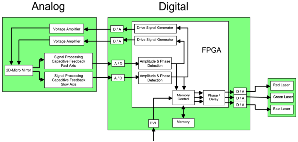
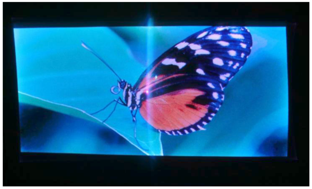
Synchronization of MEMS mirror and RGB laser sources is performed on a FPGA platform (Figure 20). Because of the high Q-factor the mirror oscillation is almost a perfect sine. That enables the accurate calculation of the instantaneous amplitude based on the measured phase and frequency. This xy-position information is used to read out the corresponding RGB pixel data, which then is used for modulating the light sources. According to the large scan angles of more than 60 degrees in both axes, laser projection based on vacuum packaged MEMS scanning mirrors enables high-resolution image and video projections (Figure 21).
Figure 20.
Analog and digital control electronics for MEMS scanning mirror based laser display

Figure 21.
Lissajous-laser-projection of a 512 × 1,024 pixel image based on a biaxial scanner with a plane glass window. The bright spot in the center of the image is caused by a direct reflex of the incoming laser beam at the glass lid of the MEMS mirror.
Figure 21.
Lissajous-laser-projection of a 512 × 1,024 pixel image based on a biaxial scanner with a plane glass window. The bright spot in the center of the image is caused by a direct reflex of the incoming laser beam at the glass lid of the MEMS mirror.

6.7. Ongoing Improvements
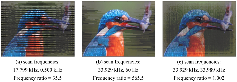
The non-homogeneous line density of the Lissajous trajectory causes one existing disturbing artifact that the picture of Figure 21 does not demonstrate. Within one period of the slow axis oscillation at 500 Hz, two interlace images of 17.8 lines each are projected. Thus, projection of the whole image of 512 lines requires at least 14.3 oscillations of the gimbal axis. That means the complete image is projected after 28.8 ms, corresponding to a frame rate of 35 Hz. However, to achieve a standard video frame rate of 60 Hz the whole number of lines needs to be projected within 16.7 ms. In addition to the low frame rate, the ratio of fast axis and slow axis frequency is disadvantageous since it leads to a scan pattern of varying line density. In a simulation of the image projection, it can be shown what the scan pattern looks like after 1/60 s (Figure 22(a)). The projected image is severely disrupted by dark patterns. In a live video demonstration with a real Lissajous laser projector, those patterns become visible as disturbing flicker effects. Hence, in order to increase the line density and in order to stabilize it even under the impact of rapidly changing laser power, there are two principle options. The first option is shown in Figure 22(b). The frequency ratio of the fast axis and the slow axis can either be chosen as high as possible, meaning that the fast axis frequency of the biaxial scanner needs to be increased and the slow axis should be decreased to the image refresh rate of 60 Hz. As an alternative, the frequency ratio can also be chosen as low as possible, meaning that the fast axis frequency and the slow axis frequency differ only by the image refresh rate of 60 Hz (Figure 22(c)). The best coverage is achieved with the high frequency ratio. However, the drawback is that the MEMS device becomes more fragile and more sensitive to vibrations by such a low resonant frequency of the slow axis. Thus, for automotive display applications the second concept based on a MEMS mirror with two fast axes of almost identical resonance frequencies could be a very robust alternative.
Figure 22.
Simulation of Lissajous laser projected images based on three different scanning mirrors. The integration time is 1/60 s and the source image has a resolution of HD720.
Figure 22.
Simulation of Lissajous laser projected images based on three different scanning mirrors. The integration time is 1/60 s and the source image has a resolution of HD720.

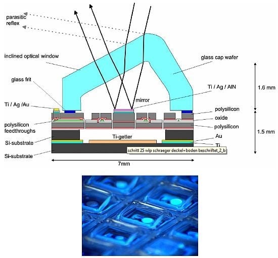
Another necessary and already achieved improvement of the display quality refers to the suppression of the bright spot which is caused by direct reflection of the incoming laser beam at the glass window in front of the oscillating mirror (Figure 21). To avoid this disturbing bright spot, there are two alternatives: Either the MEMS mirror is permanently tilted inside the cavity with respect to the plane window, or the glass cap is tilted with respect to the mirror in its non-deflected position. Both solutions spatially separate the projected image from the bright spot, provided that the angle of inclination is larger than the mechanical tilt angle amplitude. Figure 23 shows the schematic cross section of a packaged MEMS mirror with a tilted glass window. Part of the incoming laser beam does not enter the MEMS mirror cavity because it is reflected at one of the two glass interfaces. As the picture shows, this parasitic beam is reflected into a direction that is spatially separated from the angular range that can be used for laser image projection. The glass forming technology has been further developed to enable fabrication of glass wafers containing hundreds of tilted optical windows (Figure 24). Such glass cap wafers have been successfully applied for wafer level vacuum packaging. Successful suppression of the bright spot is demonstrated by projection (Figure 25).
Figure 23.
Schematic cross-section of packaged MEMS mirror with tilted optical window.

Figure 24.
Wafer level vacuum packaged MEMS mirrors with tilted glass windows.

Figure 25.
Suppressed reflex by use of a vacuum packaged mirror with tilted window.

7. Conclusions
Compact laser projection displays are of particular interest for automotive head-up displays as well as for consumer products like pico-projectors embedded in cell-phones or digital cameras. Other MEMS products like inertial sensors have already shown that wafer level packaging has become a necessity for low cost mass production. Hermetic wafer level encapsulation effectively protects the MEMS devices against contamination of all kind. Hence, also MEMS mirrors for pico-projectors will need to be packaged on wafer level. That automatically implies the need to find a solution for the reflex produced at the transparent interface. In this paper a solution has been presented that applies the tilting of the glass window which is achieved by a glass forming process on wafer level.
Since the resolution requirements of modern displays increase rapidly, MEMS scanning mirrors will have to fulfill the technical specifications of HD720 and of HD1080, i.e., large theta-d-products up to 22.5 mm × degrees, and scan frequencies exceeding 40 kHz. Low power consumption is another important property that the MEMS device has to demonstrate for all mobile applications. To meet all these requirements, increasing the Q-factor instead of increasing power consumption is the concept proposed in this paper. In this paper, a vacuum packaged MEMS mirror has been presented that achieves an optical scan angle of 86 degrees at a scan frequency of 30.8 kHz that meets the frequency and scan angle requirements of HD720. However, Finite Element simulations indicate that the dynamic deformation of this mirror will exceed lambda/10 at optical scan angles larger than 65 degrees. Based on vacuum encapsulation of MEMS mirrors, there is no principle barrier anymore to achieve the tilt angle and scan frequency requirements for HD1080 resolution. However, such a display will need to be set up as a serial arrangement of two single axis scanning mirrors, either as raster projector or in a Lissajous scan concept.
Acknowledgments
The authors want to thank Frerk Soerensen, Frank Senger, Bjoern Jensen, Juergen Hagge, Vanessa Stenchly, Christian Eisermann, Arne Schulz-Walsemann, Sascha Muehlmann, Thorsten Giese, Lars Ratzmann, Steffen Sorge, Bernd Hoefer (FHG-IOF) and Christian Mallas for their extensive support in MEMS mirror fabrication, packaging, software, optomechanics and electronics development.
References
- Hofmann, U.; Muehlmann, S.; Witt, M.; Doerschel, K.; Schuetz, R.; Wagner, B. Electrostatically driven micromirrors for a miniaturized confocal laser scanning microscope. Proc. SPIE 1999, 3878, 29–38. [Google Scholar]
- Conant, R.A.; Hagelin, P.M.; Krishnamoorthy, U.; Solgaard, O.; Lau, K.Y.; Muller, R.S. A raster-scanning full-motion video display using polysilicon micromachined mirrors. In Proceedings of IEEE Transducers Conference, Sendai, Japan, 7–10 June 1999.
- Urey, H.; Wine, D.; Lewis, J. Scanner design and resolution tradeoffs for miniature scanning displays. In Proceedings of SPIE Conference on Flat Panel Display Technology and Display Metrology, San Jose, CA, USA, 27–29 January 1999; pp. 60–68.
- Yalcinkaya, A.D.; Urey, H.; Brown, D.; Montague, T.; Sprague, R. Two-axis electromagnetic Microscanner for high resolution displays. J. Microelectromech. Syst. 2006, 15, 786–794. [Google Scholar] [CrossRef]
- Urey, H.; Wine, D.W.; Osborn, T.D. Optical performance requirements for mems-scanner based microdisplays. Proc. SPIE 2000, 4178, 176–185. [Google Scholar]
- Kurth, S.; Kaufmann, C.; Hahn, R.; Mehner, J.; Doetzel, W.; Gessner, T. A novel 24 kHz resonant scanner for high resolution laser display. Proc. SPIE 2005, 5721, 23–33. [Google Scholar]
- Gokce, S.K.; Holstrom, S.; Brown, D.; Davis, W.O.; Urey, H. A high-frequency comb-actutated resonant mems scanner for microdisplays. In Proceedings of International Conference on Optical MEMS and Nanophotonics (OMN), Istanbul, Turkey, 8–11 August 2011.
- Kirsten, M.; Wenk, B.; Ericson, F.; Schweitz, J.A.; Riethmüller, W.; Lange, P. Deposition of thick doped polysilicon films with low stress in an epitaxial reactor for surface micromachining applications. Thin Solid Films 1995, 259, 181–187. [Google Scholar] [CrossRef]
- Merz, P.; Quenzer, H.J.; Bernt, H.; Wagner, B.; Zoberbier, M. A novel micromachining technology for structuring borosilicate glass substrates. In Proceedings of IEEE Transducers Conference, Boston, MA, USA, 8–12 June 2003; pp. 258–261.
- Oldsen, M.; Hofmann, U.; Quenzer, H.J.; Wagner, B. A novel fabrication technology for waferlevel vacuum packaged microscanning mirrors. In Proceedings of the 9th Conference on Electronics Packaging Technology (EPTC), Singapore, 10–12 December 2007; pp. 303–307.
- Wine, D.W.; Helsel, M.P.; Jenkins, L.; Urey, H.; Osborn, T.D. Performance of a biaxial MEMS-based scanner for microdisplay applications. SPIE Vol. 2000, 4178, 186–196. [Google Scholar] [CrossRef]
- Ji, C.-H.; Choi, M.; Kim, S.-C.; Lee, S.-H.; Kim, S.-H.; Yee, Y.; Bu, J.-U. An electrostatic scanning micromirror with diaphragm mirror plate and diamond-shaped reinforcement frame. J. Micromech. Microeng. 2006, 16, 1033–1039. [Google Scholar] [CrossRef]
- Yalcinkaya, A.D.; Urey, H.; Brown, D.; Montague, T.; Sprague, R. Two-axis electromagnetic microscanner for high resolution displays. J. Microelectromech. Syst. 2006, 1, 968–971. [Google Scholar]
- Arslan, A.; Brown, D.; Davis, W.O.; Holmström, S.; Gokce, S.K.; Urey, H. Comb-actuated resonant torsional microscanner with mechanical amplification. J. Microelectromech. Syst. 2010, 19, 936–944. [Google Scholar] [CrossRef]
- Yoda, M.; Isamoto, K.; Chong, C.; Ito, H.; Murata, A.; Kamisuki, S.; Atobe, M.; Toshiyoshi, H. A MEMS 1-D optical scanner for laser projection display using self-assembled vertical combs and scan-angle magnifying mechanism. In Proceedings of Conference on Solid-state Sensors, Actuators and Microsystems, Seoul, Korea, 5–9 June 2005.
- Kurth, S.; Kaufmann, C.; Hahn, R.; Mehner, J.; Doetzel, W.; Gessner, T. A novel 24-kHz resonant scanner for high-resolution laser display. Proc. SPIE 2005, 5721, 23–33. [Google Scholar]
- Ko, Y.C.; Chob, J.W.; Muna, Y.K.; Jeong, H.G.; Choi, W.K.; Kima, J.W.; Park, Y.H.; Yoo, J.B.; Lee, J.H. Eye-type scanning mirror with dual vertical combs for laser display. Sens. Actuat. A 2006, 126, 218–226. [Google Scholar] [CrossRef]
- Cho, J.W.; Park, Y.H.; Ko, Y.C.; Lee, B.L.; Kang, S.J.; Chung, S.W.; Choi, W.K.; Cho, Y.C.; Chang, S.M.; Lee, J.H.; et al. Electrostatic 1D microscanner with vertical combs for HD resolution display. Proc. SPIE 2007, 6466, 64660B:1–64660B:12. [Google Scholar]
- Tachibana, H.; Kawano, K.; Ueda, H.; Noge, H. Vacuum wafer level packaged two-dimensional optical scanner by anodic bonding. In Proceedings of IEEE Conference on MEMS, Sorrento, Italy, 25–29 January 2009.
- Gokce, S.K.; Holmstrom, S.; Brown, D.; Davis, W.O.; Urey, H. A high-frequency comb-actuated resonant MEMS scanner for microdisplays. In Proceedings of Conference on Optical MEMS and Nanophotonics, Istanbul, Turkey, 8–11 August 2011.
- Hsu, S.; Klose, T.; Drabe, C.; Schenk, H. Fabrication and characterization of a dynamically flat high resolution micro-scanner. J. Opt. A: Pure Appl. Opt. 2008, 10, 44005. [Google Scholar] [CrossRef]
- Iseki, T.; Okumura, M.; Sugawara, T. High-speed and wide-angle deflection optical mems scanner using piezoelectric actuation. IEEJ Trans. Elec. Electron. Eng. 2010, 5, 361–368. [Google Scholar] [CrossRef]
- Conant, R.A.; Nee, J.T.; Lau, K.Y.; Muller, R.S. A flat high-frequency scanning micromirror. In Proceedings of Hilton Head Solid-State Sensor and Actuator Workshop, Hilton Head Island, SC, USA, June 2000; pp. 6–9.
- Hofmann, U.; Oldsen, M.; Quenzer, H.; Janes, J.; Heller, M.; Weiss, M.; Fakas, G.; Ratzmann, L.; Marchetti, E.; D’Ascoli, F.; et al. Wafer-level vacuum packaged resonant micro-scanning mirrors for compact laser projection displays. In Proceedings of Conference on MOEMS and Miniaturized Systems VII, San Jose, CA, USA, 22–23 January 2008.
© 2012 by the authors; licensee MDPI, Basel, Switzerland. This article is an open-access article distributed under the terms and conditions of the Creative Commons Attribution license (http://creativecommons.org/licenses/by/3.0/).
Share and Cite
MDPI and ACS Style
Hofmann, U.; Janes, J.; Quenzer, H.-J. High-Q MEMS Resonators for Laser Beam Scanning Displays. Micromachines 2012, 3, 509-528. https://doi.org/10.3390/mi3020509
AMA Style
Hofmann U, Janes J, Quenzer H-J. High-Q MEMS Resonators for Laser Beam Scanning Displays. Micromachines. 2012; 3(2):509-528. https://doi.org/10.3390/mi3020509
Chicago/Turabian StyleHofmann, Ulrich, Joachim Janes, and Hans-Joachim Quenzer. 2012. "High-Q MEMS Resonators for Laser Beam Scanning Displays" Micromachines 3, no. 2: 509-528. https://doi.org/10.3390/mi3020509