Fabrication of Nanopillar Micropatterns by Hybrid Mask Lithography for Surface-Directed Liquid Flow


Abstract
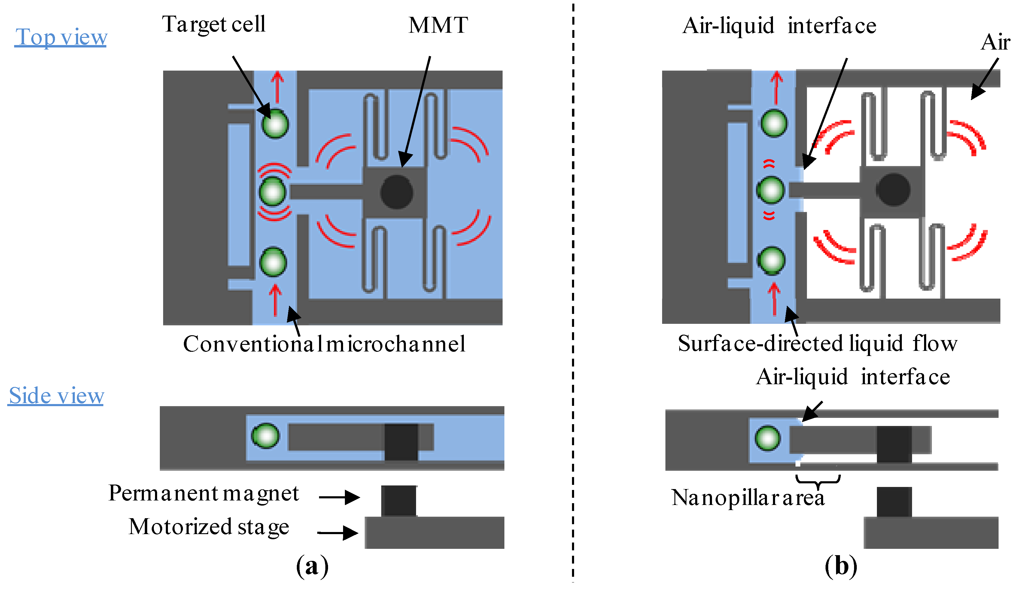
:1. Introduction

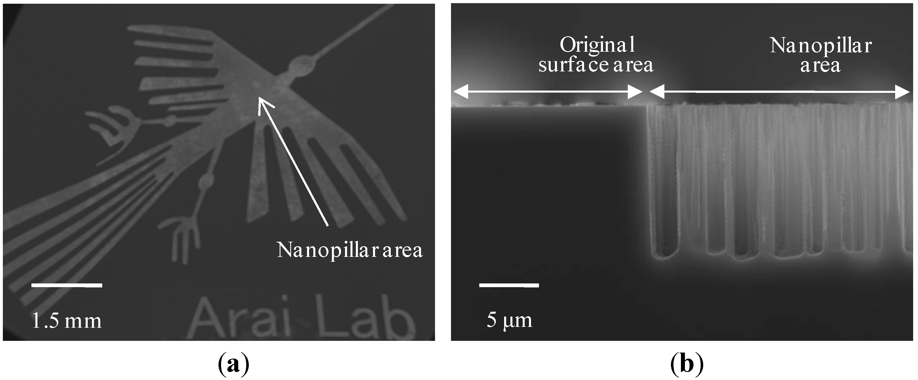
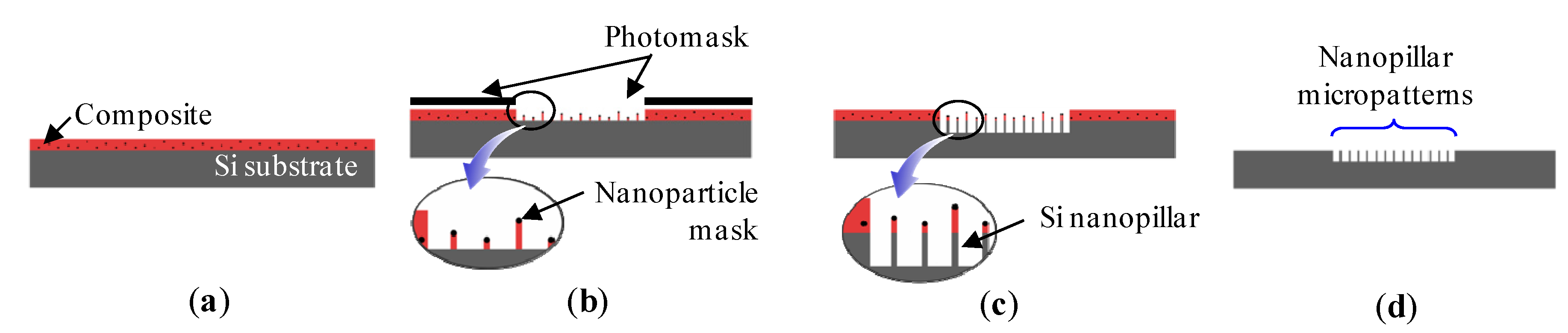
2. Fabrication of Nanopillar Micropatterns
- (1)
- It is possible to fabricate arbitrary 2D patterns using photolithography.
- (2)
- Nanopillars at the diffraction-limited size are achieved by using nanoparticles mask.
- (3)
- The density of nanopillars can be controlled by simply changing the weight ratio of the nanoparticles of the composite.
- (4)
- The height of nanopillars can also be controlled to be the same as the micropattern, which is the original surface of the substrate.

3. Results and Discussions
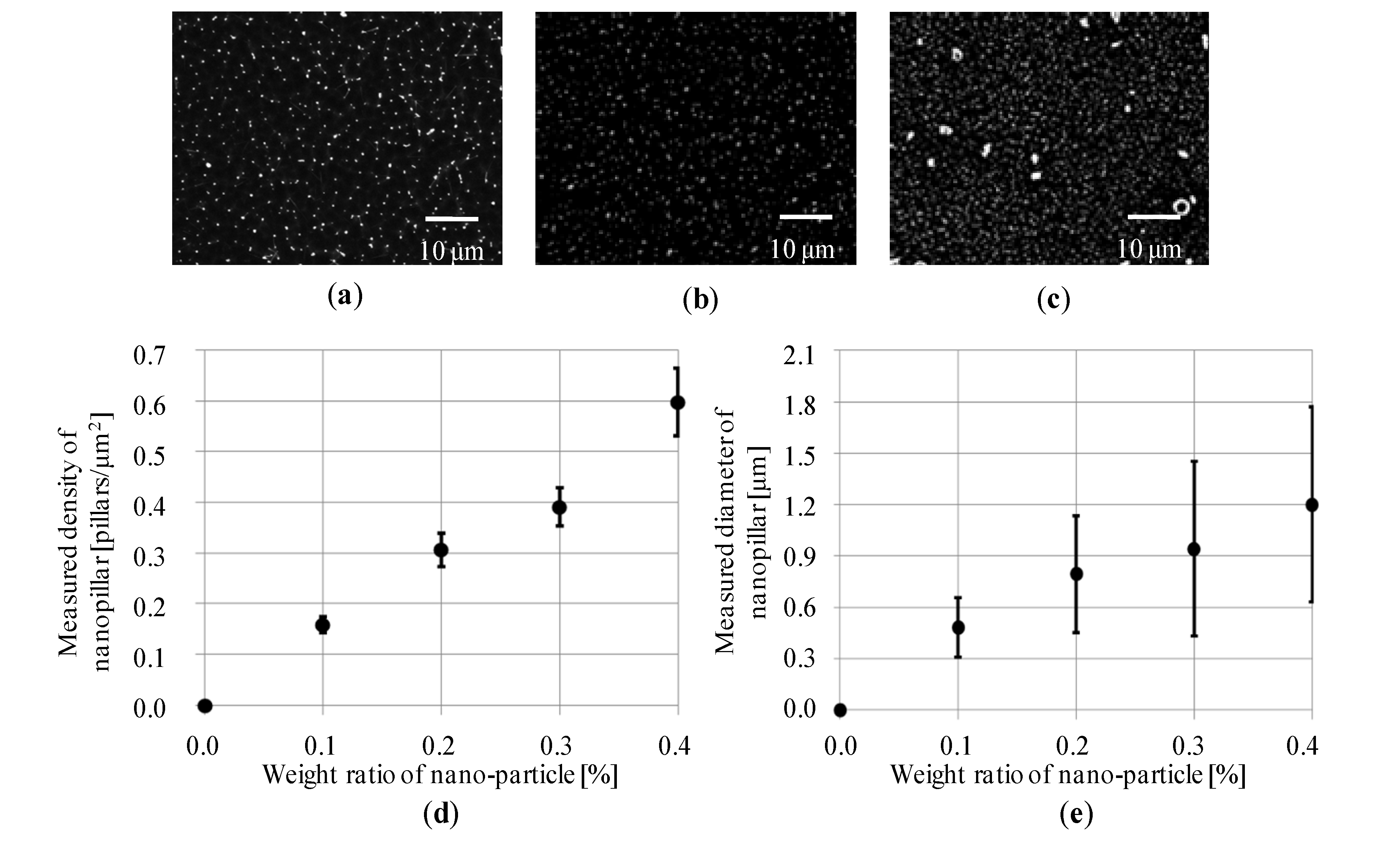
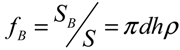
3.1. Density Control of Nanopillars

3.2. Contact Angle Control
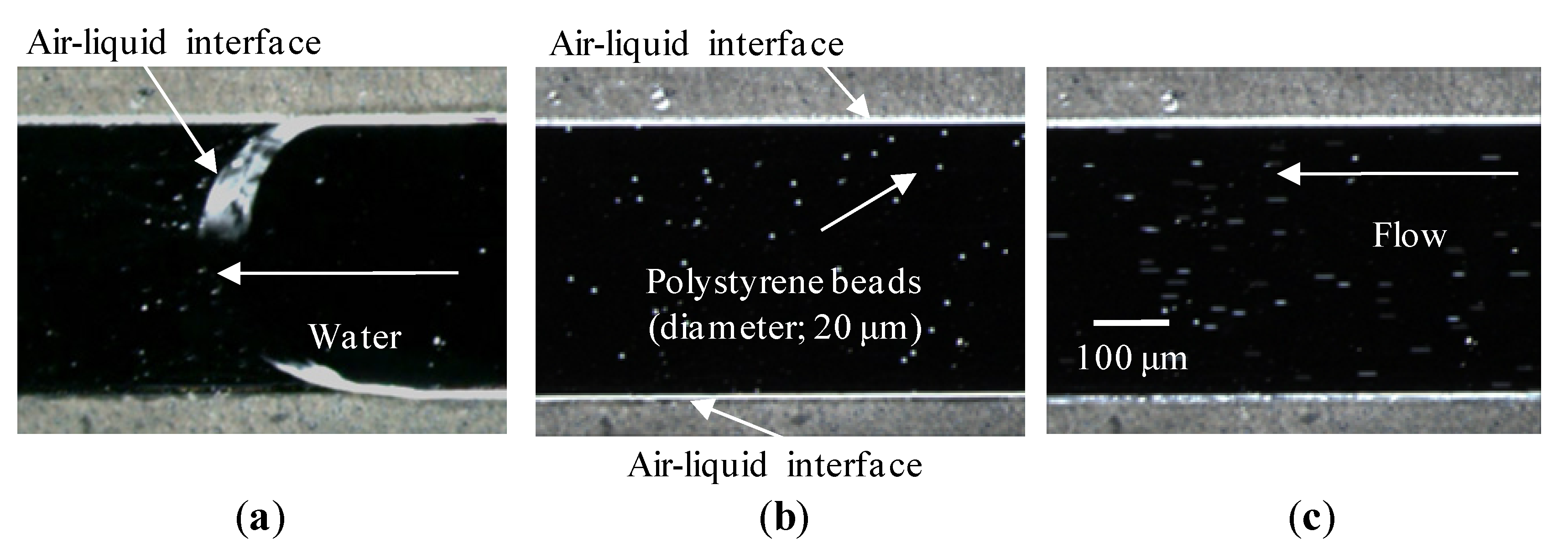
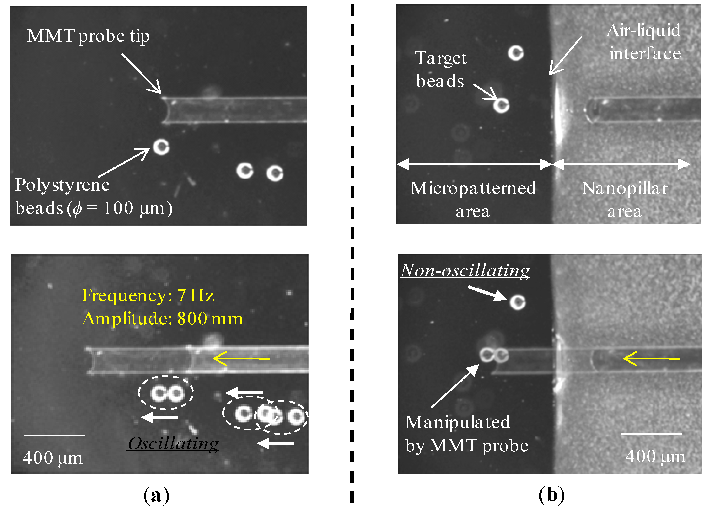
3.3. Surface-Directed Liquid Flow


4. Conclusions
Acknowledgments
References
- Wakayama, T.; Perry, A.C.F.; Zuccotti, M.; Johnson, K.R.; Yanagimachi, R. Full-term development of mice fromenucleated oocytes injected with cumulus cell nuclei. Nature 1998, 394, 369–374. [Google Scholar] [CrossRef]
- Sun, Y.; Wan, K.T.; Roberts, K.P.; Bischof, J.C.; Nelson, B.J. Mechanical property characterization of mouse zona pellucida. IEEE Trans. NanoBiosci. 2003, 2, 279–286. [Google Scholar] [CrossRef]
- Trimmer, W.S.N. Microrobots and micromechanical systems. Sens. Actuators 1989, 19, 267–287. [Google Scholar] [CrossRef]
- Arai, F.; Ogawa, M.; Fukuda, T. Selective manipulation of a microbe in a microchannel using a teleoperated laser scanning manipulator and dielectrophoresis. Adv. Rob. 1999, 13, 343–345. [Google Scholar] [CrossRef]
- Onda, K.; Arai, F. Multi-beam bilateral teleoperation of holographic optical tweezers accelerated by general-purpose GPU. Opt. Express 2012, 20, 3642–3653. [Google Scholar] [CrossRef]
- Mensing, G.A.; Pearce, T.M.; Graham, M.D.; Beebe, D.J. An externally driven magnetic microstirrer. Philos. Trans. R. Soc. Lond. Ser. A 2004, 362, 1059–1068. [Google Scholar] [CrossRef]
- Ryu, K.S.; Shaikh, K.; Goluch, E.; Fan, Z.; Liu, C. Micro magnetic stir-bar mixer integrated with parylene microfluidic channels. Lab Chip 2004, 4, 608–613. [Google Scholar] [CrossRef]
- Hu, W.; Ishii, K.S.; Ohta, A.T. Micro-assembly using optically controlled bubble microrobots. Appl. Phys. Lett. 2011, 99, 094103. [Google Scholar] [CrossRef]
- Yamanishi, Y.; Sakuma, S.; Onda, K.; Arai, F. Powerful actuation of magnetized microtools by focused magnetic field for particle sorting in a chip. Biomed. Microdevices 2008, 10, 411–419. [Google Scholar] [CrossRef]
- Yamanishi, Y.; Sakuma, S.; Kihara, Y.; Arai, F. Fabrication and application of 3-D magnetically driven microtools. J. Microelectromechanical Sys. 2010, 19, 350–357. [Google Scholar] [CrossRef]
- Hagiwara, M.; Kawahara, T.; Yamanishi, Y.; Masuda, T.; Feng, L.; Arai, F. On-chip magnetically actuated robot with ultrasonic vibration for single cell manipulations. Lab Chip 2011, 11, 2049–2054. [Google Scholar] [CrossRef]
- Hagiwara, M.; Kawahara, T.; Yamanishi, Y.; Arai, F. Precise control of magnetically driven microtools for enucleation of oocytes in a microfluidic chip. Adv. Rob. 2011, 25, 991–1005. [Google Scholar] [CrossRef]
- Atencia, J.; Beebe, D.J. Magnetically-driven biomimetic micro pumping using vortices. Lab Chip 2004, 4, 598–602. [Google Scholar] [CrossRef]
- Gassner, A.-L.; Abonnenc, M.; Chen, H.-X.; Morandini, J.; Josserand, J.; Rossier, J.S.; Busnel, J.-M.; Girault, H.H. Magnetic forces produced by rectangular permanent magnets in static microsystems. Lab Chip 2009, 9, 2356–2363. [Google Scholar]
- Stubenrauch, M.; Fischer, M.; Kremin, C.; Stoebenau, S.; Albrecht, A.; Nagel, O. Black silicon-new functionalities in microsystems. J. Micromech. Microeng. 2006, 16, S82–S87. [Google Scholar] [CrossRef]
- Onda, T.; Shibuichi, S.; Satoh, N.; Tsujii, K. Super-water-repellent fractal surfaces. Langmuir 1996, 12, 2125–2127. [Google Scholar] [CrossRef]
- Walker, B.N.; Stolee, J.A.; Pickel, D.L.; Retterer, S.T.; Vertes, A. Tailored silicon nanopost arrays for resonant nanophotonic ion production. J. Phys. Chem. C 2010, 114, 4835–4840. [Google Scholar]
- Bouaidat, S.; Hansen, O.; Bruus, H.; Berendsen, C.; Bau-Madsen, N.K.; Thomsen, P.; Wolff, A.; Jonsmann, J. Surface-directed capillary system; theory, experiments and applications. Lab Chip 2005, 5, 827–836. [Google Scholar] [CrossRef]
- Hong, L.; Pan, T. Surface microfluidics fabricated by photopatternable superhydrophobic nanocomposite. Microfluid. Nanofluid. 2011, 10, 991–997. [Google Scholar] [CrossRef]
- Jansen, H.; Boer, M.; Legtenberg, R.; Elwenspoek, M. The black silicon method: A universal method for determining the parameter setting of a fluorine-based reactive ion etcher in deep silicon trench etching with profile control. J. Micromech. Microeng. 1995, 5, 115–120. [Google Scholar] [CrossRef]
- Choi, C.H.; Kim, C.J. Large slip of aqueous liquid flow over a nanoengineered superhydrophobic surface. Phys. Rev. Lett. 2006, 96, 066001. [Google Scholar] [CrossRef]
- Martines, E.; Seunarine, K.; Morgan, H.; Gadegaard, N.; Wilkinson, C.D.W.; Riehle, M.O. Superhydrophobicity and superhydrophilicity of regular nanopatterns. Nano Lett. 2005, 5, 2097–2103. [Google Scholar] [CrossRef]
- Lee, H.; Lee, B.P.; Messersmith, P.B. A reversible wet/dry adhesive inspired by mussels and geckos. Nature 2007, 448, 338–341. [Google Scholar] [CrossRef]
- Choi, C.K.; Fowlkes, J.D.; Retterer, S.T.; Siuti, P.; Lyer, S.; Doktycz, M.J. Surface charge- and space-dependent transport of proteins in crowded environments of nanotailored posts. ACS Nano 2010, 4, 3345–3355. [Google Scholar] [CrossRef]
- Hazlett, R.D. Fractal applications: Wettability and contact angle. J. Colloid Interface Sci. 1990, 137, 527–533. [Google Scholar] [CrossRef]
© 2013 by the authors; licensee MDPI, Basel, Switzerland. This article is an open-access article distributed under the terms and conditions of the Creative Commons Attribution license (http://creativecommons.org/licenses/by/3.0/).
Share and Cite
Sakuma, S.; Sugita, M.; Arai, F. Fabrication of Nanopillar Micropatterns by Hybrid Mask Lithography for Surface-Directed Liquid Flow. Micromachines 2013, 4, 232-242. https://doi.org/10.3390/mi4020232
Sakuma S, Sugita M, Arai F. Fabrication of Nanopillar Micropatterns by Hybrid Mask Lithography for Surface-Directed Liquid Flow. Micromachines. 2013; 4(2):232-242. https://doi.org/10.3390/mi4020232
Chicago/Turabian StyleSakuma, Shinya, Masakuni Sugita, and Fumihito Arai. 2013. "Fabrication of Nanopillar Micropatterns by Hybrid Mask Lithography for Surface-Directed Liquid Flow" Micromachines 4, no. 2: 232-242. https://doi.org/10.3390/mi4020232