1. Introduction
During the past 5 decades there has been a huge improvement in micro- and nano-fabrication processes. A plethora of different techniques, machines and materials have been developed in order to keep pace with the technological requirements of our society. The metric that is normally used to track the progress of a fabrication process is based on the minimum achievable dimensions by the lithographic technique used within the process. As an example, CMOS foundries have evolved from full wafer ultra-violet (UV) optical lithography (minimum dimensions around 1 um) to deep UV (DUV) using a stepped exposure across the wafer (minimum dimensions below 100 nm). One of the major challenges of nanofabrication lies in the huge cost of the lithography machines and their operation, exponentially increasing when reducing pattern size. This is not only true for optical-based lithography. In fact, the second most used nanolithography technique (after DUV) is electron beam lithography (EBL), which also entails costly machines and operation.
Several technologies have been proposed over the last few years as alternative nanolithographic methods to be used on large scale: multi-beam electron lithography, self-assembly based lithography, nanoimprint lithography (NIL) [
1], nanostencil lithography (nSL) [
2],
etc. These two latter options offer a very high resolution (low minimum dimensions), choice of pattern size and shapes, and the costs can be pushed to a fraction of what the more standard lithography techniques mentioned in the previous paragraph require.
NIL is based on the imprinting of a stamp with nanopatterns on a polymer. The resulting patterned polymer layer can be used as a mask for subsequent etching or to do lift-off after metallization. nSL is based on patterned thin membranes that physically mask the deposition of metal [
2,
3,
4,
5], the implantation of ions [
6] or the etching of the underlying substrate [
7]. nSL is being increasingly utilized because it is a resistless technique that allows operation in several substrates, including pre-patterned [
8] and polymeric [
9]. To give a few examples, it has been used to fabricate metallic nanowires [
10], nanodot arrays for surface plasmon resonance [
11], and nano-electro-mechanical resonators integrated with CMOS circuitry [
12].
NIL and nSL rely on the accuracy of the aforementioned solid stamps and perforated membranes (stencils) respectively. Therefore, in order to minimize costs it is required to develop an inexpensive way of producing stamps and stencils. This might be very important for NIL, mostly in the cases where high pressures are utilized to imprint in the polymer, given the fact that stamps partially lose their properties after every use due to wearing. The usual procedure to achieve this is the replication of an EBL-made stamp. To do this, it is necessary to do an imprinting, a subsequent lift-off and finally a pattern transfer using the deposited metal as a hard mask [
13]. By replicating the original stamp, it is possible to increase by about one order of magnitude the amount of imprints that can be generated from one single EBL.
In this paper we show an alternative solution, which consists of the use of an EBL-made nanostencil to fabricate NIL stamps. By doing this, we eliminate some of the steps for the stamp fabrication with no resist, no solvents and no baking processes being used. In addition, stencil lithography can be used in any clean room (metal evaporators are a basic tool) and it is not necessary to have full wafer NIL machines to achieve a cost-effective stamp replication. Indeed, the lifetime of a stencil has been proven to be longer than a dozen times [
14], providing a simple and cheap method for the fabrication of stamps for NIL.
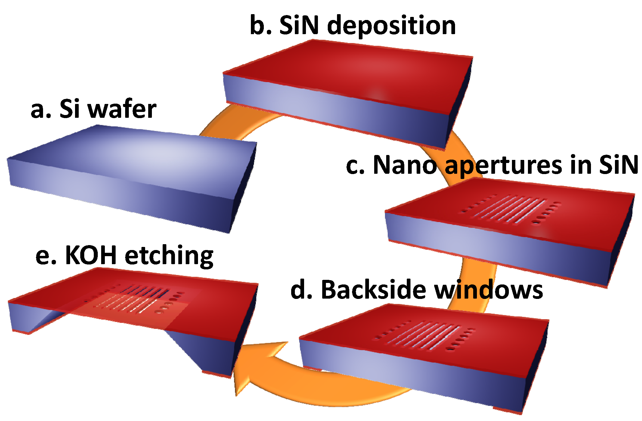
2. Stencil Fabrication
For this work, full wafer stencils are used. The fabrication starts with a double sided polished Silicon wafer (100 mm in diameter) (
Figure 1a). A layer of LPCVD (Low Pressure Chemical Vapor Deposition) low stress silicon nitride (LS-SiN) (100 to 500 nm thick, to be chosen depending on the particular application and design that is being targeted) is deposited at 840 °C (
Figure 1b) on both sides of the wafer. A lithography step is performed on the front-side of the wafer via EBL, using ZEP as the electron-sensitive resist. Then, the nitride layer is patterned using an ICP 601-E dry etcher from Alcatel, with 20 sccm of C
2F
6 as the etching gas, at 0.5 Pa with 450 platen power and 1200 W coil power (
Figure 1c). Once those patterns are transferred into the nitride, the functional apertures are opened on the front-side. Subsequently, another lithography step is performed on the backside (UV-lithography) to define the windows for KOH bulk micromachining on the backside (
Figure 1d). Finally, the release of the membranes is made using a KOH etching (60 °C, 40% in weight;
Figure 1e).
Figure 1.
Simplified stencil fabrication process flow. The fabrication starts with (a) double side polished silicon wafers, where a layer of low stress silicon nitride (LS-SiN) is deposited on both sides of the wafer (b). The thickness depends on the particular dimension requirements of the application. (c) LS-SiN is patterned on the front side by using electron beam lithography (EBL) and reactive ion etching. (d) LS-SiN is patterned on the backside in order to define the windows for the subsequent KOH etching (e), which actually releases the membranes.
The thickness of the nitride layer is chosen depending on the required stencil characteristics. The optimum value is a trade-off between the mechanical stability of the membrane and the smallest aperture size. On the one hand, the thicker the membrane, the larger deformations it can endure [
15]. On the other hand, the aspect ratio—membrane thickness/aperture width—needs to be ≤2 due to fabrication restrictions [
16], which means that in order to have small patterns, thin membranes are required.
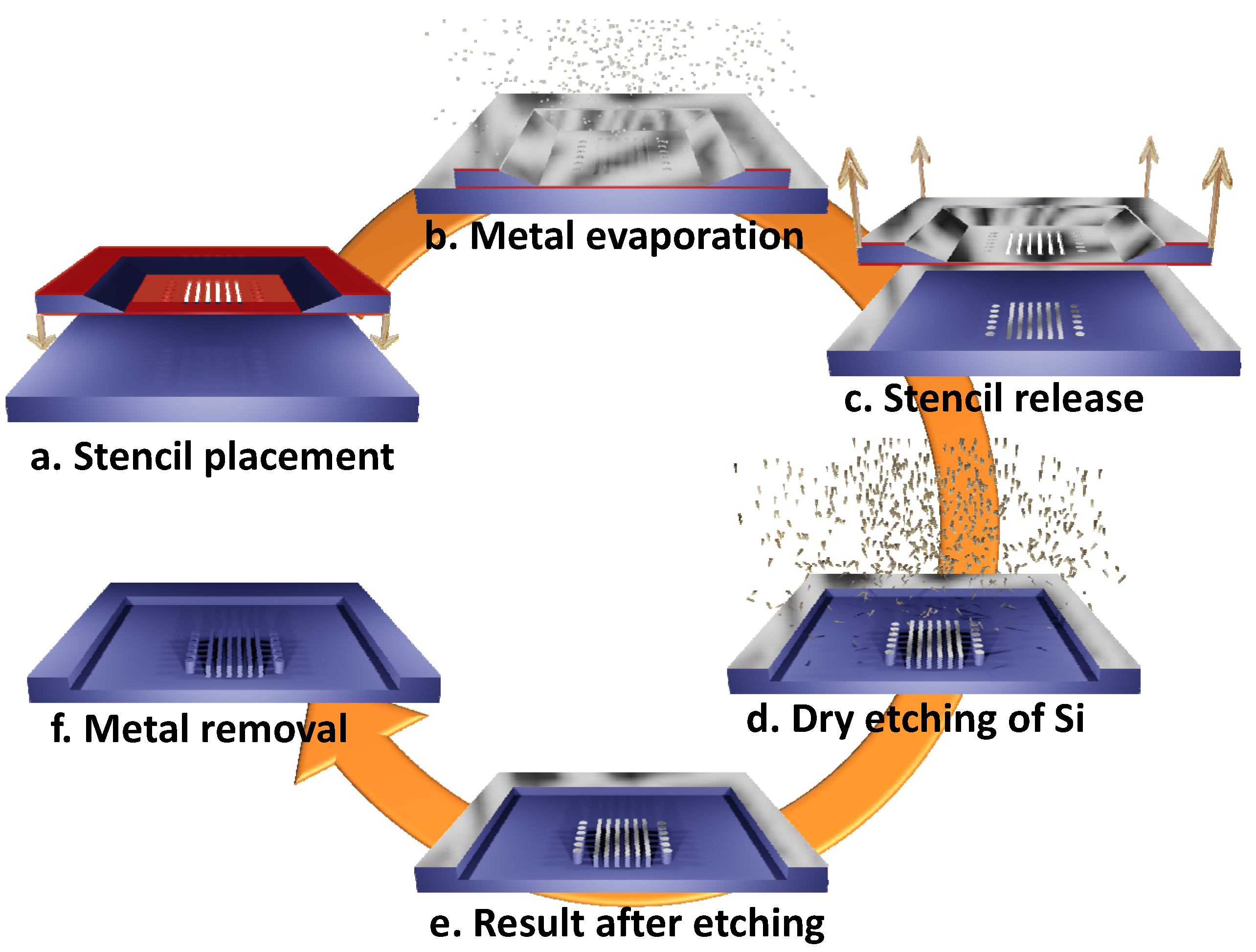
3. Stamp Fabrication
Using the stencils described in the previous section, we perform the fabrication of NIL stamps in silicon by following a similar procedure to that described elsewhere [
17,
18]. We first place the stencil on top of a 100 mm diameter Si wafer, deposit a thin aluminum layer (25 nm, e-beam evaporated,
P = 10
−6 mbar, 0.1 nm/s, the sample being placed at a distance of 1 m from the metal source with an average evaporation angle of 0°) and withdraw the stencil from the substrate (
Figure 2a–c). Once the stencil is removed, metal patterns are visible on the substrate but distortion of the patterns (blurring) can be observed [
19,
20]. We then perform the etching of the Si to define the stamp itself. A short aluminum etching is performed prior to the Si etching. This is done to remove the very-thin layer that is spread around the patterns due to surface diffusion of Al [
20,
21]. Si etching is performed using an ICP 601-E dry etcher from Alcatel with a mixture of 100 sccm of SF
6 and 100 sccm of C
4F
8 at 3 Pa with 50 W platen power and 1800 W coil power (
Figure 2d,e). Finally, Al leftovers are etched using a wet chemical etching (Al-etch, commercially available) and an anti-sticking self-assembled monolayer (SAM) is deposited on the stamp (
Figure 2f).
Figure 2.
Nanoimprint lithography (NIL) stamp fabrication process flow. The fabrication starts with (a) silicon wafers, where the stencil is placed to perform (b) a localized deposition of metal (Al) and (c) subsequently removed from the substrate. A short corrective etching is performed to remove a very thin metal layer that spreads due to surface diffusion. Subsequently, the transfer of the metal patterns into the Si is performed via dry etching (d, e) and eventually the metal is removed via wet chemical etching (f). The last detail is the deposition of an anti-sticking self-assembled monolayer.
This fabrication process flow (with slight modifications) can be also applied to stamps made out of different materials. The use of Si stamps is preferred for thermal NIL, but for UV-NIL a transparent stamp is required and this technique can be used to pattern, e.g., glass wafers into a usable stamp. The slight modifications in the process flow consist of a different etching recipe for the stamp material and, in addition, the choice of a different metal to attain a sufficiently high selectivity so that the stamp can be properly patterned.
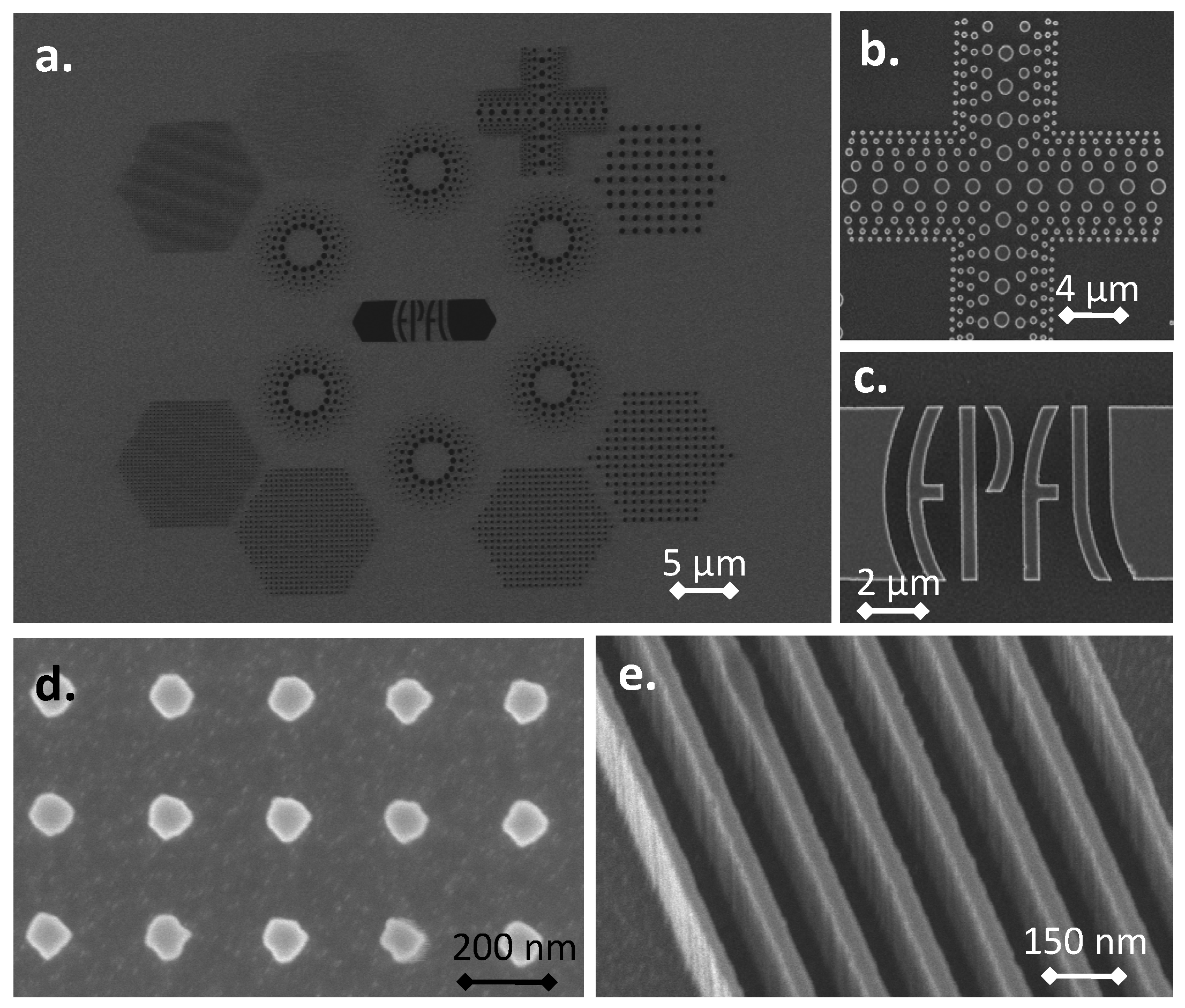
Figure 3 shows some typical results obtained following the fabrication process flows described above. In particular,
Figure 3a shows the nano-apertures in a stencil membrane. On the right,
Figure 3b,c shows the transfer of some of these apertures into a Si substrate, yielding a stamp.
Figure 3d,e shows some of the smallest features in the fabricated stamps: 100 nm pillars (
Figure 3d) and 50 nm lines (
Figure 3e). Across the whole wafer, pattern sizes are within ±5 nm of the stencil aperture sizes (extracted from the measurement of 50 different structures across the wafer).
Figure 3.
SEM micrographs showing fabrication results. (a) Detail of a nanostencil membrane. (b) and (c) show some of the patterns in (a) after the transfer to the Si has been performed. (d) and (e) show the parts of the stamp with the smallest size designs (100 nm in diameter pillars; 50 nm wide lines). Stamp features’ dimensions lie within ±10 nm of the stencil apertures’ dimensions.
4. Stamp Validation
In order to prove the validity of the fabricated stamps, thermal NIL is performed with all of them. Two different resists are used: mr-L 7010 (thickness of 100 nm) and mr-L 7030 (thickness of 300 nm), from microresist technology. We compare the behavior of the fabricated stamps using stencil lithography with the behavior of stamps directly fabricated by EBL and a stamp acquired from NIL Technology. The results are indistinguishable, with replication of the stamps’ patterns within ±10 nm (extracted from the measurement of 50 structures across the whole wafer).
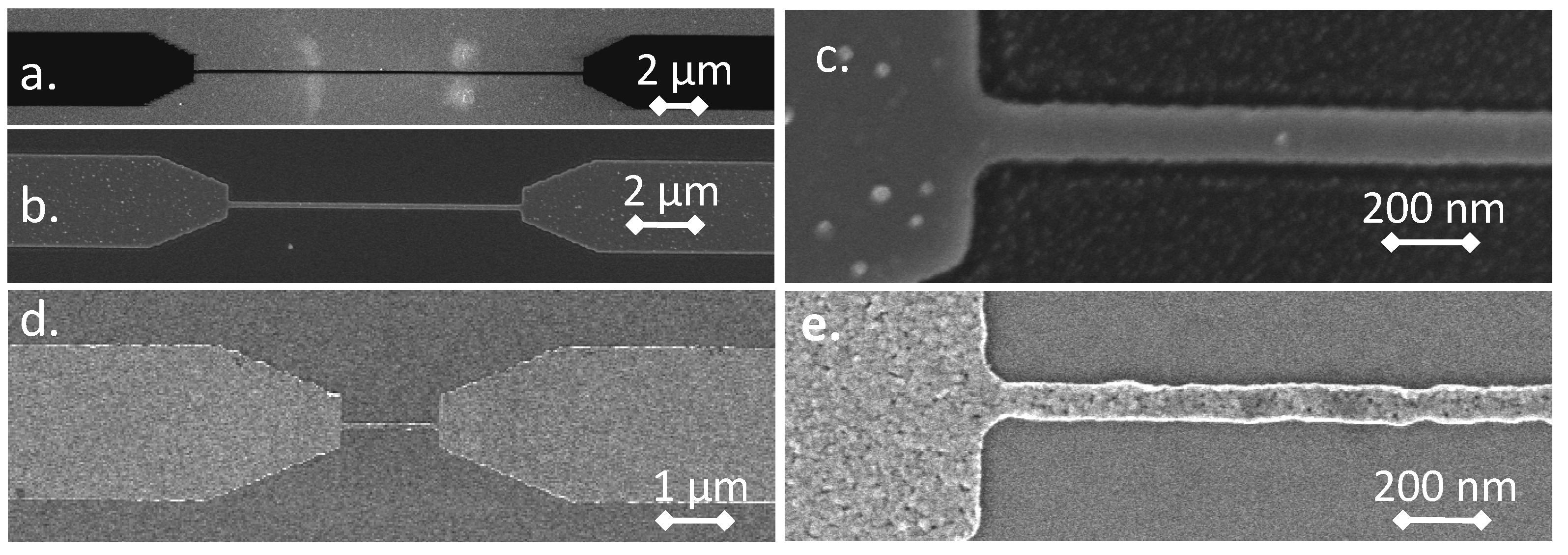
Figure 4 shows a particular example of the use of stencil-fabricated NIL stamps. We use an EBL-fabricated stencil with nanowire designs (
Figure 4a). After the stamp is fabricated in Si, every nanowire pattern is present in the stamp, with minimum features of 100 nm
Figure 4b,c). After imprinting in mr-L 7010, we perform a short (5 s) oxygen plasma with high DC bias (in order to maintain the dimensions as much as possible). We then evaporate a thin aluminum layer (50 nm thick) using e-beam evaporation. After the subsequent and necessary lift-off, the minimum achieved aluminum nanowire width was 100 nm (
Figure 4d,e).
Figure 4.
Validation of NIL stamp. (a) EBL-fabricated nanostencil. (b) and (c) are stamp details corresponding to nanowire designs. (d) and (e) resulting metal patterns after lift-off.
Figure 4.
Validation of NIL stamp. (a) EBL-fabricated nanostencil. (b) and (c) are stamp details corresponding to nanowire designs. (d) and (e) resulting metal patterns after lift-off.
5. Conclusions
In this paper, we have shown that stencil lithography is a suitable technique for the fabrication of NIL stamps with features down to 50 nm size. We have also shown how those stamps can successfully be used to perform NIL. As a proof of that, the pattern transfer into the resist, and subsequently into the metal, of aluminum nanowires of 100 nm width is demonstrated. We believe this is the first demonstration of this cost-efficient and useful fabrication technique for the replication of NIL stamps. Even though some type of structures (e.g., concentric rings) might prove difficult to transfer, the overall result of this technique might be interesting for fabrication facilities where standard NIL-based stamp replication is not possible.
