A Fluidic Interface with High Flow Uniformity for Reusable Large Area Resonant Biosensors

 , and
, and 
Abstract
:1. Introduction
2. Design and Simulation
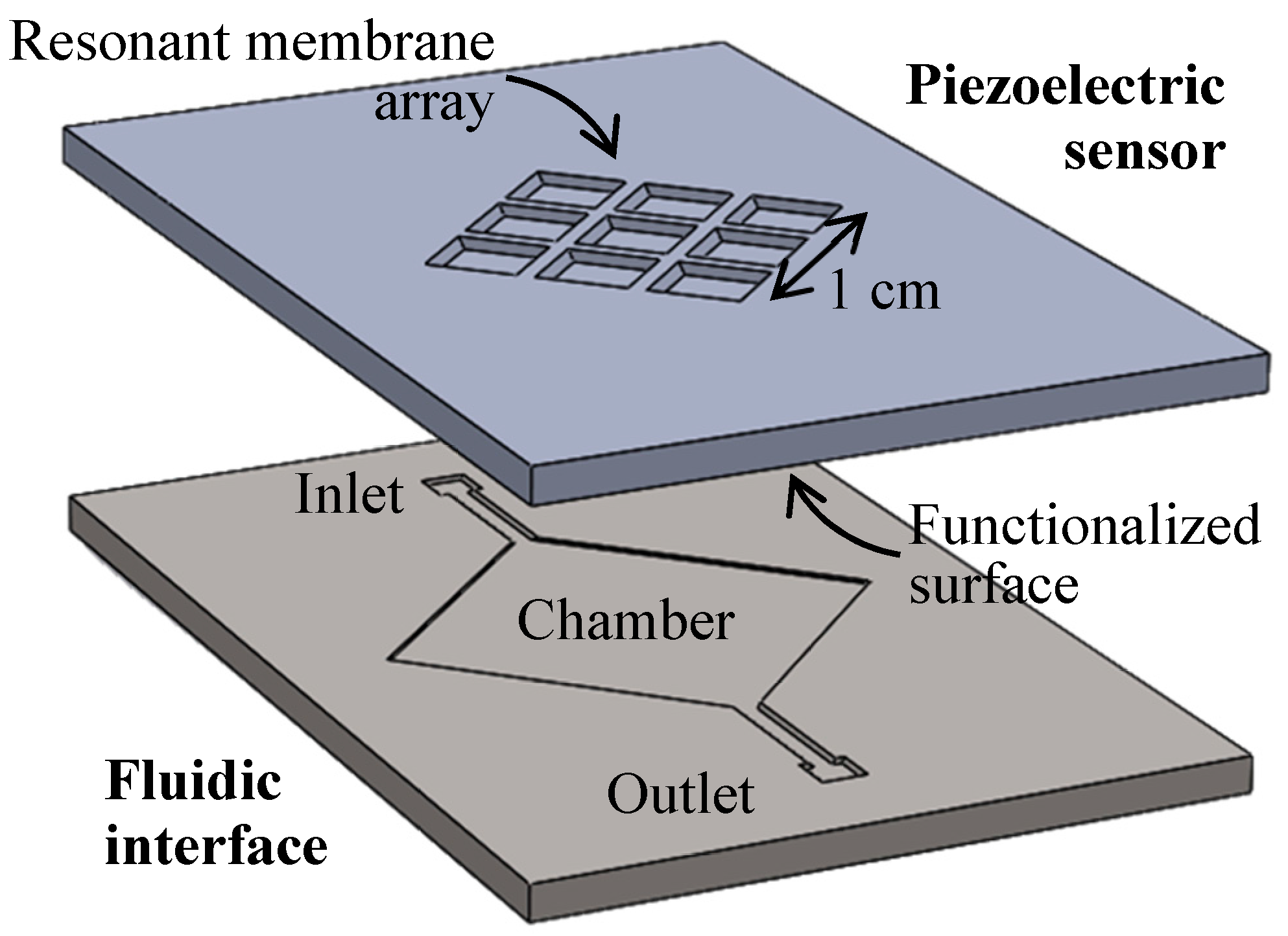
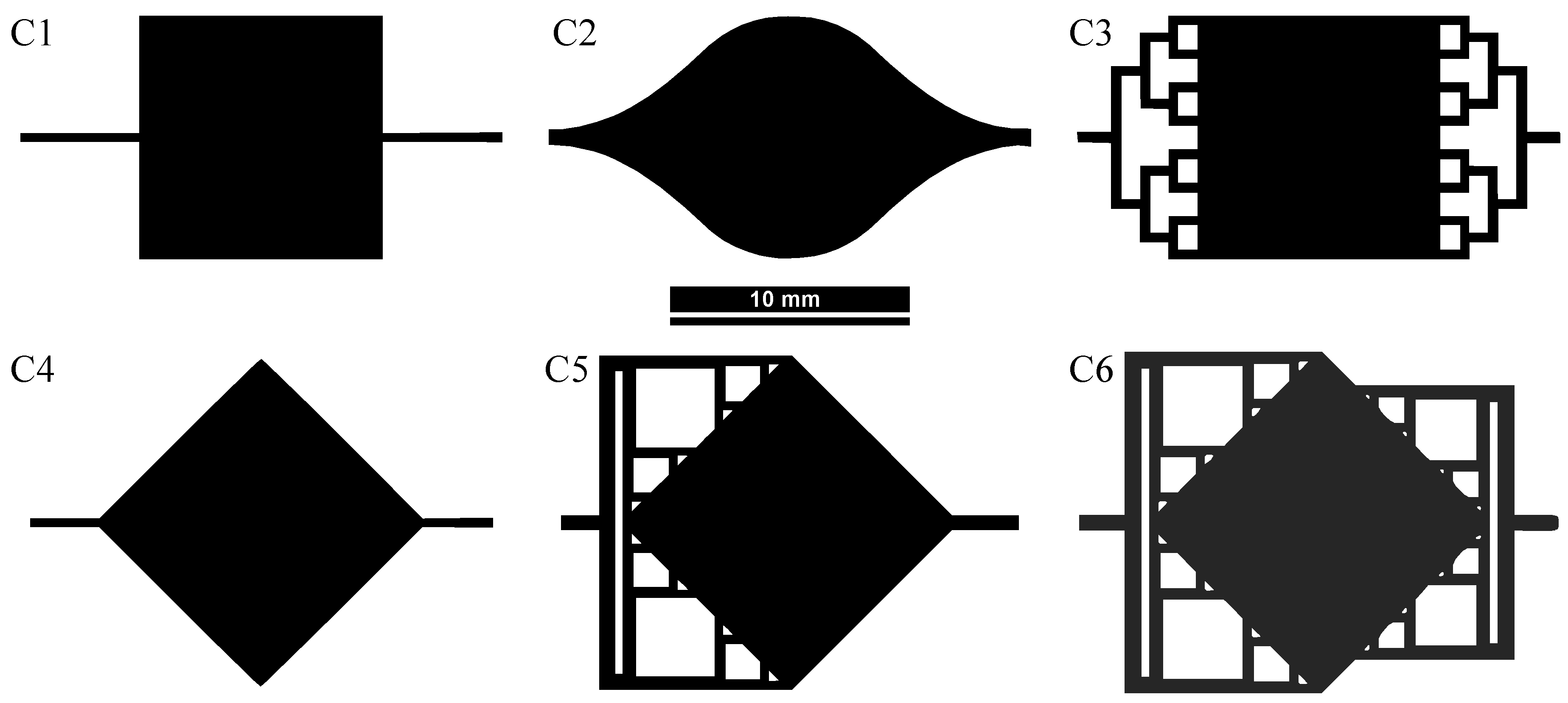
2.1. Fluidic Interface Characteristics
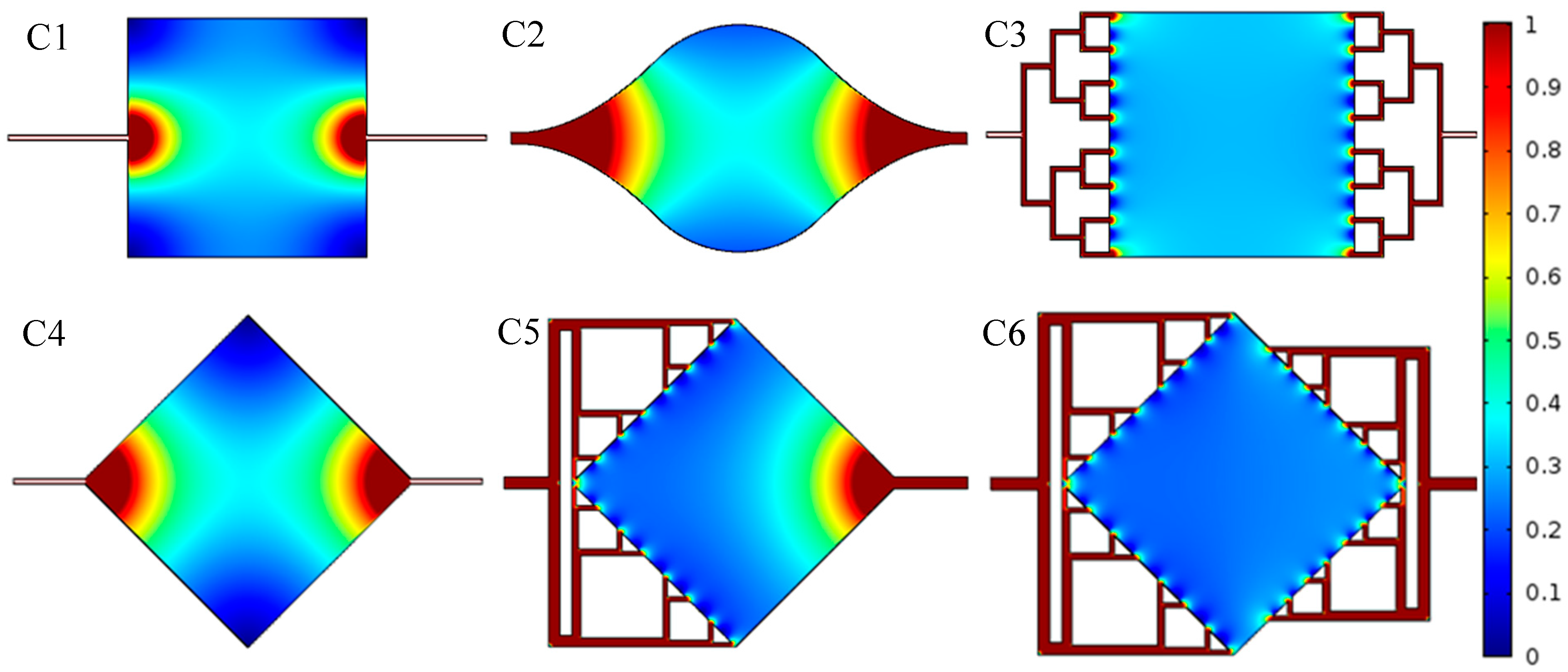
2.2. Flow Simulation
3. Microfabrication
3.1. Layout of Microfluidic Circuit
3.2. Microfabrication Process
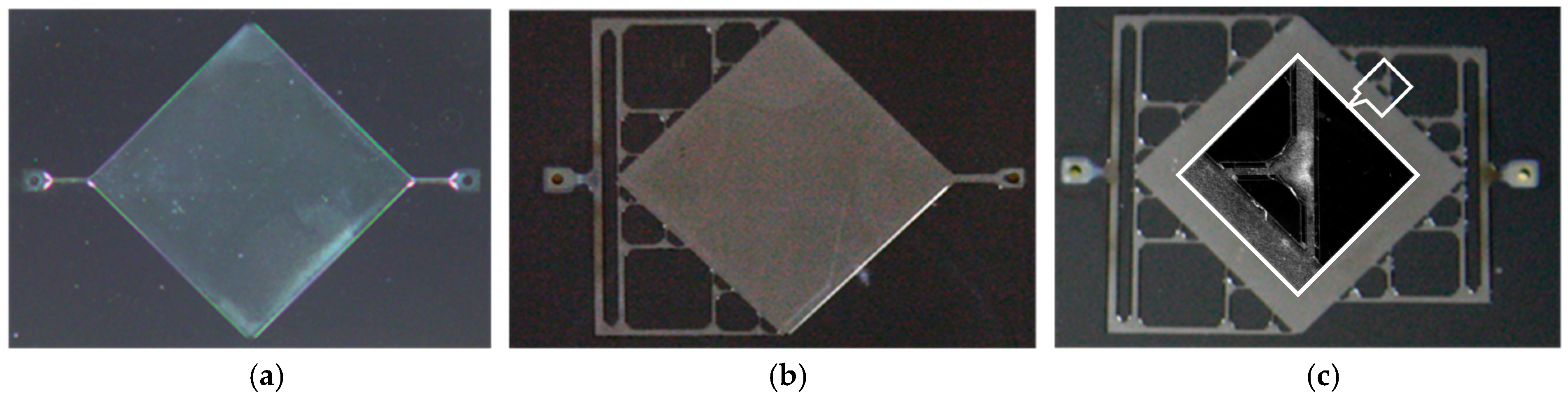
3.3. Micromachined Structures
4. Experimental Characterization
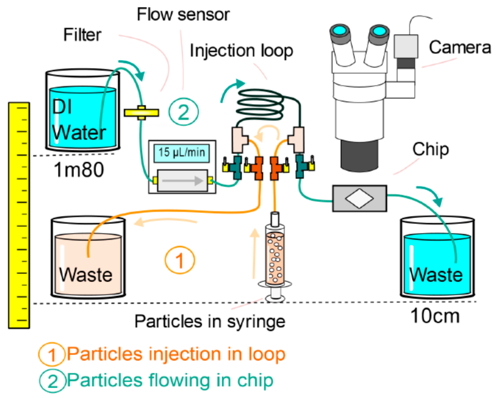
4.1. Experimental Setup
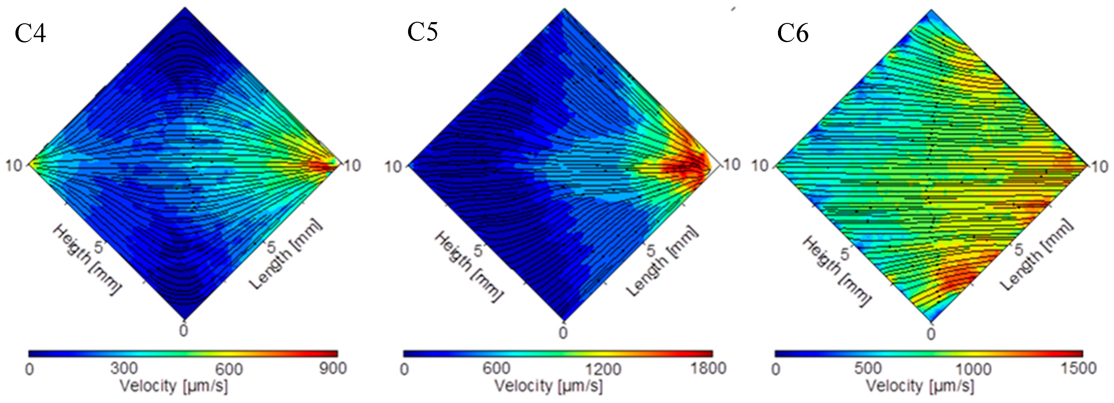
4.2. Results
5. Conclusions
Supplementary Materials
Supplementary File 1Acknowledgments
Author Contributions
Conflicts of Interest
References
- Wingqvist, G.; Yantchev, V.; Katardjiev, I. Mass sensitivity of multiplayer thin film resonant BAW sensors. Sens. Actuators A 2008, 148, 88–95. [Google Scholar] [CrossRef]
- Lin, R.-E.; Chen, Y.-C.; Chang, W.-T.; Cheng, C.-C.; Kao, K.-S. Highly sensitive mass sensor using film bulk acoustic resonator. Sens. Actuators A 2008, 147, 425–429. [Google Scholar] [CrossRef]
- Bao, L.; Qu, X.; Chen, H.; Su, X.; Yao, S.; Wei, W. A bulk acoustic wave viscosity sensor for determination of lysozyme based on lysis of micrococcus lysodeikeicus. Microchim. Acta 1999, 132, 61–65. [Google Scholar] [CrossRef]
- Branch, D.W.; Brozik, M.S. Low-level detection of a bacillus anthracis stimulant using love-wave biosensors on 36° YX LiTaO. Biosens. Bioelectron. 2004, 19, 849–859. [Google Scholar] [CrossRef] [PubMed]
- Ergezen, E.; Hong, S.; Barbee, A.K.; Lec, R. Real time monitoring of the effects of Heparan Sulfate Proteoglycan and surface charge ont the cell adhesion process using thickness shear mode senso. Biosens. Bioelectron. 2007, 22, 2256–2260. [Google Scholar] [CrossRef] [PubMed]
- Saitakis, M.; Tsortos, A.; Gizeli, E. Probing the interaction of a membrane receptor with a surface-attached ligand using whole cells on acoustic biosensor. Biosens. Bioelectron. 2010, 25, 1688–1693. [Google Scholar] [CrossRef] [PubMed]
- Squires, T.M.; Messinger, R.J.; Manalis, S.R. Making it stick: Convection, reaction and diffusion in surface-based biosensors. Nat. Biotechnol. 2008, 26, 417–426. [Google Scholar] [CrossRef] [PubMed]
- Saias, L.; Autebert, J.; Malaquin, L.; Viovy, J.-L. Design, modeling and characterization of microfluidic architectures for high flow rate, small footprint microfluidic systems. Lab Chip 2011, 11, 822–832. [Google Scholar] [CrossRef] [PubMed]
- Pálovics, P.; Ender, F.; Rencz, M. Microfluidic flow-through chambers for higher performance. In Proceedings of the 2017 Symposium on Design, Test, Integration and Packaging of MEMS/MOEMS (DTIP), Bordeaux, France, 29 May–1 June 2017. [Google Scholar]
- Liao, W.; Wang, N.; Wang, T.; Xu, J.; Han, X.; Liu, Z.; Zhang, X.; Yu, W. Biomimetic microchannels of planar reactors for optimized photocatalytic efficiency of water purification. Biomicrofluidics 2016, 10, 014123. [Google Scholar] [CrossRef] [PubMed]
- Emerson, D.R.; Cieślicki, K.; Gu, X.; Barber, R.W. Biomimetic design of microfluidic manifolds based on a generalised Murray’s law. Lab Chip 2006, 6, 447–454. [Google Scholar] [CrossRef] [PubMed]
- Cao, C.; Kim, J.P.; Kim, B.W.; Chae, H.; Yoon, H.C.; Yang, S.S.; Sim, S.J. A strategy for sensitivity and specificity enhancements in prostate specific antigen-α 1-antichymotrypsin detection based on surface plasmon resonance. Biosens. Bioelectron. 2006, 21, 2106–2113. [Google Scholar] [CrossRef] [PubMed]
- Piliarik, M.; Bocková, M.; Homola, J. Surface plasmon resonance biosensor for parallelized detection of protein biomarkers in diluted blood plasma. Biosens. Bioelectron. 2010, 26, 1656–1661. [Google Scholar] [CrossRef] [PubMed]
- Bienaime, A.; Liu, L.; Elie-Caille, C.; Leblois, T. Design and microfabrication of a lateral excited gallium arsenide biosensor. Eur. Phys. J. Appl. Phys. 2012, 57, 21003. [Google Scholar] [CrossRef]
- Gardeniers, H.; Luttge, R.; Berenschot, E.; Boer, M.D.; Yeshurun, S.; Hefetz, M.; Oever, M.V.; Berg, A.V.D. Silicon Micromachined hollow microneedles for transdermal liquid transport. J. Microelectromech. Syst. 2003, 12, 855–862. [Google Scholar] [CrossRef]
- Archer, M.J.; Ligler, F.S. Fabrication and Characterization of Silicon Micro-funnels and tapered micro-channels for stochastic sensing application. Sensors 2008, 8, 3848–3872. [Google Scholar] [CrossRef] [PubMed]
- Bienaime, A.; Leblois, T.; Lucchi, G.; Blondeau-Patissier, V.; Ducoroy, P.; Boireau, W.; Elie-Caille, C. Reconstitution of a protein monolayer on thiolates functionalized GaAs surface. Int. J. Nanosci. 2012, 11, 1240018. [Google Scholar] [CrossRef]
- White, F. Fluid Mechanics; McGraw Hil: New York, NY, USA, 2003. [Google Scholar]
- Mortensen, N.; Okkels, F.; Bruus, H. Electrohydrodynamics of binary electrolytes driven by modulated surface potentials. Phys. Rev. E 2005, 71, 057301. [Google Scholar] [CrossRef] [PubMed]
- Koh, K.-S.; Chin, J.; Chia, J.; Chiang, C.-L. Quantitative studies on PDMS-PDMS interface bonding with piranha solution and its swelling effect. Micromachines 2012, 3, 427–441. [Google Scholar] [CrossRef]
- Rumens, C.V.; Ziai, M.A.; Belsey, K.E.; Batchelor, J.C.; Holder, S.J. Swelling of PDMS networks in solvent vapours; applications for passive RFID wireless sensors. J. Mater. Chem. C 2015, 3, 10091–10098. [Google Scholar] [CrossRef]
- Yablonovitch, E.; Hwang, D.M.; Gmitter, T.J.; Florez, L.T.; Harbison, J.P. Van der Waals bonding of GaAs epitaxial liftoff films onto arbitrary substrates. Appl. Phys. Lett. 1990, 56, 2419–2421. [Google Scholar] [CrossRef]
- Williams, K.R.; Gupta, K.; Wasilik, M. Etch rates for micromachining processing-Part II. J. Microelectromech. Syst. 2003, 12, 761–778. [Google Scholar] [CrossRef]
- Khan, M.S.; Williams, J.D. Fabrication of solid state nanopore in thin silicon membrane using low cost multistep chemical etching. Materials 2015, 8, 7389–7400. [Google Scholar] [CrossRef] [PubMed]
- Liu, H.; Chollet, F. Layout Controlled One-Step Dry Etch and Release of MEMS Using Deep RIE on SOI Wafer. J. Microelectromech. Syst. 2006, 15, 541–547. [Google Scholar]
- Seidel, H.; Csepregi, L.; Heuberger, A.; Baumgärtel, H. Anisotropic etching of crystalline silicone in alkaline solution. J. Electrochem. Soc. 1990, 137, 3612–3625. [Google Scholar] [CrossRef]
- Shikida, M.; Nambara, K.; Kozumi, T.; Sasaki, H.; Odagaki, M.; Sato, K.; Ando, M.; Furuta, S.; Asaumi, K. A model explaining mask corner undercut phenomena in anisotropic silicon etching: A saddle point in the etching rate diagram. Sens. Actuators A 2002, 97–98, 758–763. [Google Scholar] [CrossRef]
- Frühauf, J.; Hannemann, B. Anisotropic multi-step etch process of silicon. J. Micromech. Microeng. 1997, 7, 137–140. [Google Scholar] [CrossRef]
- Elwenspoek, M.; Jansen, H.V. Silicon Micromachining; Cambridge University Press: Cambridge, UK, 2004. [Google Scholar]
- Schroder, H.; Obermeier, E. A new model for Si{100} convex corner undercutting in anisotropic KOH etching. J. Micromech. Microeng. 2000, 10, 163–170. [Google Scholar] [CrossRef]
- Pal, P.; Sato, K.; Chandru, S. Fabrication techniques of convex corners in a {100}-silicon wafer using bulk micromachining: A review. J. Micromech. Microeng. 2007, 17, R111–R133. [Google Scholar] [CrossRef]
- Pal, P.; Sato, K. Complex three-dimensional structures in Si{100} using wet bulk micromachining. J. Micromech. Microeng. 2009, 19, 105008. [Google Scholar] [CrossRef]
- Biswas, K.; Das, S.; Kal, S. Analysis and prevention of convex corner undercutting in bulk micromachined silicon microstructures. Microelectron. J. 2006, 37, 765–769. [Google Scholar] [CrossRef]
- Wacogne, B.; Zeggari, R.; Sadani, R.; Gharbi, T. A very simple compensation technique for bent V-grooves in KOH etched (100) silicon when thin structures or deep etching are required. Sens. Actuators A 2006, 126, 264–269. [Google Scholar] [CrossRef]
- Bonnet, D.; Barthes, M.; Bailly, Y.; Girardot, L.; Ramel, D.; Grenier, A.; Guyon, D. PIV in a running automotive engine: Simultaneous velocimetry for intake manifold runners. J. Flow Vis. Image Process. 2012, 19, 239–253. [Google Scholar] [CrossRef]
- Amini, H.; Lee, W.; Di Carlo, D. Inertial microfluidic physics. Lab Chip 2014, 14, 2739–2761. [Google Scholar] [CrossRef] [PubMed]


| Material | Material Cost | Compat. with GaAs | Fabrication Cost | Resistance to Aging | Resistance to Regen. | Biocompat. |
|---|---|---|---|---|---|---|
| PDMS | low | medium | low | low | medium | high |
| Polymer | low | medium | low | low | low | medium |
| GaAs | high | high | medium | high | high | medium |
| Glass | medium | low | high | high | medium | high |
| Silicon dry | medium | medium | high | high | high | medium |
| Silicon wet | medium | medium | medium | high | high | high |
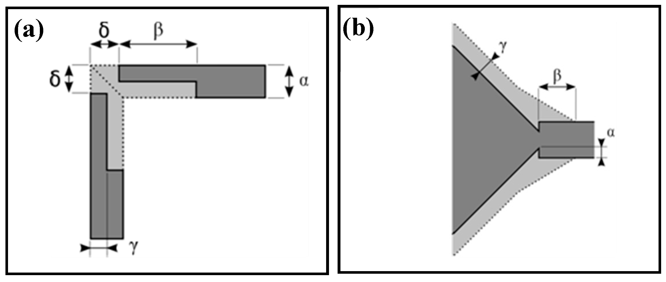
| Set | α | β | γ | δ |
|---|---|---|---|---|
| Q1 | 100 | 170 | 50 | 0 |
| Q2 | 100 | 170 | 50 | 50 |
| Q3 | 100 | 210 | 25 | 50 |
| I1 | 50 | 200 | 75 | - |
© 2017 by the authors. Licensee MDPI, Basel, Switzerland. This article is an open access article distributed under the terms and conditions of the Creative Commons Attribution (CC BY) license (http://creativecommons.org/licenses/by/4.0/).
Share and Cite
Azzopardi, C.-L.; Lacour, V.; Manceau, J.-F.; Barthès, M.; Bonnet, D.; Chollet, F.; Leblois, T. A Fluidic Interface with High Flow Uniformity for Reusable Large Area Resonant Biosensors. Micromachines 2017, 8, 308. https://doi.org/10.3390/mi8100308
Azzopardi C-L, Lacour V, Manceau J-F, Barthès M, Bonnet D, Chollet F, Leblois T. A Fluidic Interface with High Flow Uniformity for Reusable Large Area Resonant Biosensors. Micromachines. 2017; 8(10):308. https://doi.org/10.3390/mi8100308
Chicago/Turabian StyleAzzopardi, Charles-Louis, Vivien Lacour, Jean-François Manceau, Magali Barthès, Dimitri Bonnet, Franck Chollet, and Thérèse Leblois. 2017. "A Fluidic Interface with High Flow Uniformity for Reusable Large Area Resonant Biosensors" Micromachines 8, no. 10: 308. https://doi.org/10.3390/mi8100308