Transparent Ferroelectric Capacitors on Glass


Luxembourg Institute of Science and Technology, Department of Materials Research and Technology, 41 rue du Brill, Belvaux, L-4422, Luxembourg
*
Author to whom correspondence should be addressed.
Micromachines 2017, 8(10), 313; https://doi.org/10.3390/mi8100313
Submission received: 6 September 2017
/
Revised: 8 October 2017
/
Accepted: 17 October 2017
/
Published: 20 October 2017
(This article belongs to the Special Issue Piezoelectric MEMS)
Abstract
:We deposited transparent ferroelectric lead zirconate titanate thin films on fused silica and contacted them via Al-doped zinc oxide (AZO) transparent electrodes with an interdigitated electrode (IDE) design. These layers, together with a TiO2 buffer layer on the fused silica substrate, are highly transparent (>60% in the visible optical range). Fully crystallized Pb(Zr0.52Ti0.48)O3 (PZT) films are dielectrically functional and exhibit a typical ferroelectric polarization loop with a remanent polarization of 15 μC/cm2. The permittivity value of 650, obtained with IDE AZO electrodes is equivalent to the one measured with Pt electrodes patterned with the same design, which proves the high quality of the developed transparent structures.
1. Introduction
In parallel to the development of technologies on silicon, there is a large panel of new functions dedicated to transparent substrates and more specifically to glass [1]. This should involve completely transparent functional layers such as transistors [2] and sensing elements [3]. Transparent pixels or photovoltaic devices have already been published in the literature [4]. Similarly to the More than Moore trend, one can think of developing new devices on glass with optical or mechanical coupling in order to multiply applications. For instance, it has recently been suggested that haptic functions can be added on mobile phone screens through piezoelectric ceramics [5]. It would be ideal to achieve completely transparent stacks on glass so as not to perturb light transmission when it comes to adding new functionalities to screens. We will eventually target transparent piezoelectric stacks in order to fabricate haptic devices. More specifically, we want to study lead zirconate titanate (PZT) films, piezoelectric films with one of the highest reported piezoelectric coefficients, deposited on glass. Moreover, we aim at suppressing the bottom electrode in order to potentially improve the overall transparency. It induces that top electrodes will be interdigitated. Our top choice of electrode is Al-doped zinc oxide (AZO) because of its optical transparency and electrical conductivity [6]. In addition, it does not contain any rare and/or harmful components such as indium in indium tin oxide (ITO) electrodes.
The deposition of PZT on glass substrates, unlike PZT films on silicon, has barely been studied. All examples with electrical results involved a bottom electrode, which was made of Pt or transparent conductive oxides, such as ITO [7] or fluorine-doped tin oxide (FTO) [8]. Khodorov et al. deposited La-doped PZT via the sol–gel method on tin oxide-coated glass substrate [9]. The reflection in the visible range for 130-nm-thick La-doped PZT (PLZT) did not exceed 20%, and no electrical results were performed. Ohno et al. showed that 1.1-µm-thick PZT with compositions close to the morphotropic phase boundary (MPB, corresponding to Zr/Ti = 52/48), deposited via chemical solution deposition (CSD) on soda lime glass and covered with CSD ITO exhibited a dielectric permittivity εr close to 1000, a remanent polarization as large as 36 µC/cm², and a longitudinal piezoelectric coefficient d33 reaching 120 pC/N after thermal treatment at 600 °C [10]. The transmittance of the stack without top electrode was around 60% in the visible optical range, which was a substantial improvement with respect to Khodorov et al. Liu et al. [11] obtained very similar results on Co-doped PZT also deposited via CSD on an ITO/glass substrate. More recently, Bayraktar et al. [12] focused on the crystalline quality of PZT films grown on glass and reported epitaxial growth of MPB PZT by utilizing Ca2Nb3O10 and Ti0.87O2 nanosheets as crystalline buffer layers, combined with ITO or Pt/ITO as bottom electrode. Another interesting approach leading to epitaxial films has been proposed by Terada et al. [13], who first grew PZT on MgO and then transferred the layers to glass substrates, though Pt electrodes have been utilized. The unique example of a fully transparent and electrically functional PZT-based stack on glass substrates was published in 2007 by Uprety et al. [14]. The studied stack was ITO/LNO/PZT/LNO/ITO (where LNO stands for LaNiO3) on glass. The PZT was 90-nm-thick, and the overall transparency of the final device capacitor was around 50% before the deposition of the top electrode. In this paper, we propose to improve the overall transparency of the same kind of MPB PZT stack by suppressing the bottom electrode and adopting an in-plane interdigitated electrode (IDE) configuration, similar to what has been performed on silicon more than a decade ago [15].
2. Experimental Section
A 2”-diameter and 500-µm-thick substrate made of optical grade fused silica with roughness Ra <1 nm has been used. A buffer layer was needed between glass and PZT to avoid cracks. Here, this buffer layer was made of 20-nm-thick oxidized titanium deposited via evaporation at 25 °C and annealed at 700 °C in air. Such high temperature infers the complete oxidation of Ti, which stabilizes titanium oxide with respect to the subsequent steps. PZT with MPB composition—meaning Zr/Ti = 52/48—was deposited by spin coating three successive layers of “PZT-E1” commercial sol precursors from MMC (Mitsubishi Materials Corporation, Tokyo, Japan). Each of the three PZT layers was spun, dried at 130 °C for 5 min, and pyrolyzed at 350 °C for 5 min on hot plate in air. A final annealing step performed in a box furnace at 700 °C in air for 30 min induced the crystallization of the 200-nm-thick PZT film in the desired perovskite structure. The 115-nm-thick AZO IDE electrodes were then deposited via atomic layer deposition and patterned through a lift-off process using lift-off resist (LOR) Shipley resist in order to generate an undercut below a resist layer (1813 Shipley). Reference samples made of sputtered 100-nm-thick Pt electrodes with the same IDE design were also realized by standard lithography/ion beam etching process. The absolute values of electric field E, relative dielectric permittivity ε’ and polarization P were extracted from the measurements as recently described by Nigon et al. [16]. Because the gap and width of the fingers are significantly larger than the thickness of the film (a, b >> tf), the effective gap a + Δa (Δa = 1.324 × tf) was used in the calculations.
X-ray diffraction patterns were obtained with a Panalytical diffractometer in θ-2θ configuration, - 2θ being the measurement angle of the detector with respect to X-ray incident beam on the sample at angle θ. The light transmittance of the stack was measured on a TECAN (Tecan Group Ltd., Zürich, Switzerland) absorbance instrument. The Agilent atomic force microscope (AFM) was used to measure root-mean-square (RMS) surface roughness. The permittivity-electric field (ε’-E) curves and polarization-electric field (P-E) loops were collected with an Aixacct set-up.
3. Results
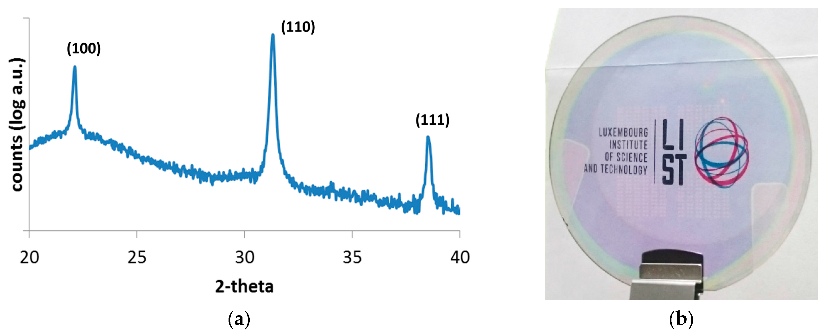
Figure 1a shows the X-ray diffraction pattern of crystallized PZT films on glass. The perovskite structure is the only visible phase. No secondary phase such as pyrochlore has been detected. There is no preferred crystalline orientation as one could expect on an amorphous substrate such as fused silica. The RMS value obtained from 5 × 5 μm2 areas by AFM is 2.0 nm. Figure 1b shows a top view of the transparent finalized substrate—fused silica/TiO2/PZT/AZO—as observed with optical microscopy. Note that the logo is not printed on the wafer but is visible through the latter. PZT film is homogeneous and did not encounter cracks during the fabrication process. Our experiments have shown that a buffer layer of TiO2 with a minimum thickness of 10 nm is mandatory to avoid cracks. For thinner layers or no buffer layer at all, PZT crystallizes but exhibits cracks.
The main drawback of TiO2 is that it induces a purplish color that limits the device’s transparency, as can be seen in Figure 1b. Fused silica exhibits transmittance beyond 93% in the visible spectral range (cf. Figure 2). This transmittance decreases down to 65% around λ = 400 nm after TiO2 has been deposited. Adding PZT creates Fabry–Perot oscillations but does not strongly impact the overall transmittance. It also shifts the minimum wavelength that can cross the wafer from 300 nm with TiO2 to 340 nm if one takes 20% transmittance as a reference. The final 115-nm-thick AZO slightly improves the stack transmittance probably because of the index matching effect. Indeed, the ZnO refractive index is around 2.0, whereas that of PZT is larger, around 2.4. Consequently, capping PZT with ZnO-based material smoothens the gap and therefore acts as an index matching layer. AZO main drawback is that it stops transmittance below 360 nm. All in all, the stack transmittance is higher than 60% in the range from 400 nm to 1000 nm. As mentioned in the introduction, Uprety et al. reported 50% transmittance on their transparent piezoelectric stack involving ITO as the bottom electrode [14]. Therefore, our strategy to suppress the bottom electrode helps in improving transparency.
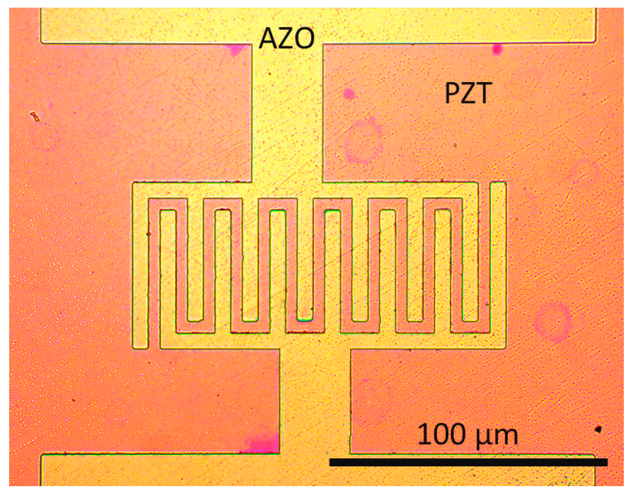
Making electrically functional transparent piezoelectric devices without bottom electrode infers that both electrodes have to be processed on the top of the piezoelectric layer. To do so, we patterned AZO IDE electrodes as shown in Figure 3. Various gaps (5, 10, and 20 µm) were processed. Although AZO is not as conductive as ITO (typical sheet resistance of 250 Ω2 for 100-nm-thick films in our case), it only involves abundant and low-cost metals (aluminium and zinc).
Figure 4a shows the relative permittivity ε’ and dielectric losses tanδ versus the DC electric field of the 7-tooth IDE structure reported in Figure 3. Both curves display the typical hysteretic behavior of ferroelectric films, with respective zero-field values of permittivity and tanδ of 650 and 0.03. Contrary to what is generally observed in metal–insulator–metal structures (MIM), the curves are very symmetrical with respect to the Y-axis. This is a direct consequence of the symmetrical IDE structure that has been processed with the same metal. The losses are very low—below 1%—at voltages as large as 400 kV/cm. It evidences the good quality of PZT, but also the compatibility of AZO electrodes with PZT in this IDE structure.
Figure 4b represents the same characterization on the same IDE structure, though with Pt electrodes. The difference lies in the maximum electric field applied, which is only 200 kV/cm with Pt. Indeed, this structure was unable to withstand larger field because of the ion milling etching step that weakened PZT and/or induced Pt re-deposition. It ended up with strong extrinsic leakage at a high electric field. In Figure 4, one can spot that permittivity values are very similar for both AZO and Pt electrodes. The latter is considered as the reference metal for PZT. Therefore, it shows that AZO stands for a convincing transparent alternative to Pt in order to contact PZT structures.
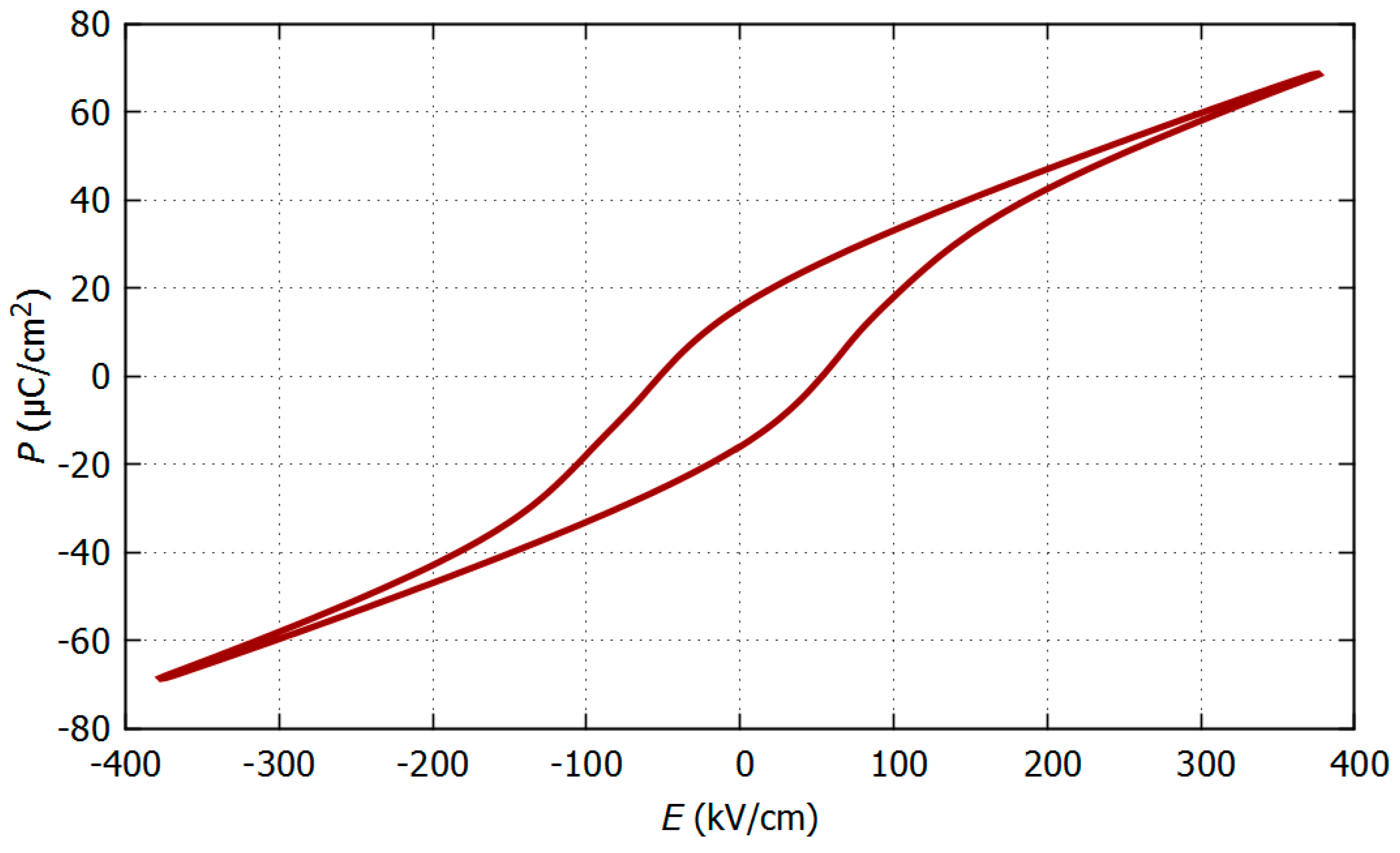
Finally, a clear ferroelectric behaviour is observed on the polarization-electric field (P-E) loop of PZT on glass with AZO electrodes, as shown in Figure 5. The extracted value of remanent polarization Pr is 15 μC/cm2, which is approximately half the value reported for 500-nm-thick (100) MPB PZT on Si with Pt IDE electrodes, but comparable to its counterpart in MIM geometry [17]. The calculated coercive field Ec is 52 kV/cm. The slanted shape of the loop is a measurement artefact due to relatively large stray capacitance compared to the total capacitance value (measured on IDE structures and shown in Figure 3). We wanted to ensure that this tilted loop was not induced by AZO’s rather high resistivity, so we compared it with Pt top electrodes patterned with the same design. Both loop shape and coercive voltage are very similar to what has been observed with AZO electrodes. In addition, we found that AZO equivalent resistance of Figure 3 is around 700 Ω. This impedance is negligible compared to PZT, which lies in the GΩ range (C~1 pF) during the P-E loop collection performed at 100 Hz. Consequently, AZO’s higher resistance has no significant influence on the P-E loop’s shape.
4. Conclusions
In this paper, we have shown that it is possible to make functional transparent ferroelectric structures with PZT and IDE AZO electrodes. The measured permittivity, dielectric losses, and polarization values of 650, 0.03, and 15 μC/cm2, respectively, have confirmed typical ferroelectric behavior, which is a pre-requisite of piezoelectric ferroelectric materials such as PZT. The main advantage of the proposed structure is the absence of bottom electrode, which implies improved transparency of the whole PZT stack (>60% in the visible range) if one compares with Uprety et al.’s [14] study with the ITO bottom electrode.
Acknowledgments
The authors thank FNR, the Luxembourg Research National Agency (Fonds National de la Recherche) for granting this study through COFERMAT project (grant number FNR/P12/4853155/Kreisel) belonging to the PEARL scheme. We also thank Patrick Grysan for his help on AFM measurements.
Author Contributions
Daniele Sette and Emmanuel Defay conceived and designed the experiments; Daniele Sette, Stéphanie Girod, and Sebastjan Glinsek performed the experiments; Renaud Leturcq, Sebastjan Glinsek, Daniele Sette, and Emmanuel Defay analyzed the data; Sebastjan Glinsek and Emmanuel Defay wrote the paper.
Conflicts of Interest
The authors declare no conflict of interest.
References
- Stoppa, M.; Chiolerio, A. Wearable Electronics and Smart Textiles: A Critical Review. Sensors 2014, 14, 11957–11992. [Google Scholar] [CrossRef] [PubMed]
- Fortunato, E.; Barquinha, P.; Martins, R. Oxide semiconductor thin-film transistors: A review of recent advances. Adv. Mater. 2012, 24, 2945–2986. [Google Scholar] [CrossRef] [PubMed]
- Martins, R.; Fortunato, E.; Nunes, P.; Ferreira, I.; Marques, A.; Bender, M.; Katsarakis, N.; Cimalla, V.; Kiriakidis, G. Zinc oxide as an ozone sensor. J. Appl. Phys. 2004, 96, 1398–1408. [Google Scholar] [CrossRef]
- Fortunato, E.; Ginley, D.; Hosono, H.; Paine, D.C. Transparent conducting oxides for photovoltaics. MRS Bull. 2007, 32, 242–247. [Google Scholar] [CrossRef]
- Bernard, F.; Gorisse, M.; Casset, F.; Chappaz, C.; Basrour, S. Design, Fabrication and Characterization of a Tactile Display Based on AlN Transducers. Procedia Eng. 2014, 87, 1310–1313. [Google Scholar] [CrossRef]
- Sette, D.; Girod, S.; Godard, N.; Adjeroud, N.; Chemin, J.B.; Leturcq, R.; Defay, E. Transparent piezoelectric transducers for large area ultrasonic actuators. In Proceedings of the 30th IEEE International Conference on Micro Electro Mechanical Systems (MEMS), Las Vegas, NV, USA, 22–26 January 2017; pp. 793–796. [Google Scholar]
- Cotroneo, V.; Davis, W.N.; Marquez, V.; Reid, P.B.; Schwartz, D.A.; Johnson-Wilke, R.L.; Trolier-McKinstry, S.E.; Wilke, R.H. Adjustable grazing incidence X-ray optics based on thin PZT films. In Proceedings of the International Society for Optics and Photonics (SPIE), San Diego, CA, USA, 12–16 August 2012; p. 850309. [Google Scholar]
- Pérez-Tomás, A.; Lira-Cantú, M.; Catalan, G. Above-Bandgap Photovoltages in Antiferroelectrics. Adv. Mater. 2016, 28, 9644–9647. [Google Scholar] [CrossRef] [PubMed]
- Khodorov, A.; Gomes, M.J. Preparation and optical characterization of lanthanum modified lead zirconate titanate thin films on indium-doped tin oxide-coated glass substrate. Thin Solid Films 2006, 515, 1782–1787. [Google Scholar] [CrossRef]
- Ohno, T.; Fujimoto, M.; Suzuki, H. Preparation and characterization of PZT thin films on ITO/glass substrate by CSD. Key Eng. Mater. 2006, 301, 41–44. [Google Scholar] [CrossRef]
- Liu, Z.; Liu, Q.; Liu, H.; Yao, K. Electrical properties of undoped PZT and Co-doped PCZT films deposited on ITO/glass substrates by a sol–gel method. Phys. Stat. Sol. A 2005, 202, 1834–1841. [Google Scholar] [CrossRef]
- Bayraktar, M.; Chopra, A.; Bijkerk, F.; Rijnders, G. Nanosheet controlled epitaxial growth of PbZr0.52Ti0.48O3 thin films on glass substrates. Appl. Phys. Lett. 2014, 105, 132904. [Google Scholar] [CrossRef]
- Terada, K.; Suzuki, T.; Kanno, I.; Kotera, H. Hidetoshi Kotera, Fabrication of single crystal PZT thin films on glass substrates. Vacuum 2007, 81, 571–578. [Google Scholar] [CrossRef]
- Uprety, K.K.; Ocola, L.E.; Auciello, O. Growth and characterization of transparent Pb (Zi, Ti)O3 capacitor on glass substrate. J. Appl. Phys. 2007, 102, 084107. [Google Scholar] [CrossRef]
- Zhang, Q.Q.; Gross, S.J.; Tadigadapa, S.; Jackson, T.N.; Djuth, F.T.; Trolier-McKinstry, S. Lead zirconate titanate films for d33 mode cantilever actuators. Sens. Actuators A 2003, 105, 91–97. [Google Scholar] [CrossRef]
- Nigon, R.; Raeder, T.M.; Muralt, P. Characterization methodology for lead zirconate titanate thin films with interdigitated electrode structures. J. Appl. Phys. 2017, 121, 204101. [Google Scholar] [CrossRef]
- Chidambaram, N.; Balma, D.; Nigon, R.; Mazzalai, A.; Matloub, R.; Sandu, C.S.; Muralt, P. Converse mode piezoelectric coefficient for lead zirconate titanate thin film with interdigitated electrode. J. Micromech. Microeng. 2015, 25, 045016. [Google Scholar] [CrossRef]
Figure 1.
(a) The θ-2θ pattern of 200-nm-thick Pb(Zr0.52Ti0.48)O3 (PZT) film deposited by spin coating on TiO2/fused silica and crystallized at 700 °C. All peaks correspond to the perovskite structure; (b) Optical image of a 2’’-diameter wafer coated with 20 nm of TiO2, 200 nm of PZT, and 115 nm of patterned Al-doped zinc oxide (AZO), the latter being visible in the central area of the wafer. TiO2 exhibits a purplish color. Note that the logo is visible through the glass wafer.

Figure 2.
Optical transmission spectra from 232 nm to 1000 nm measured on the successive stacks of AZO/PZT/TiO2/fused silica.
Figure 2.
Optical transmission spectra from 232 nm to 1000 nm measured on the successive stacks of AZO/PZT/TiO2/fused silica.
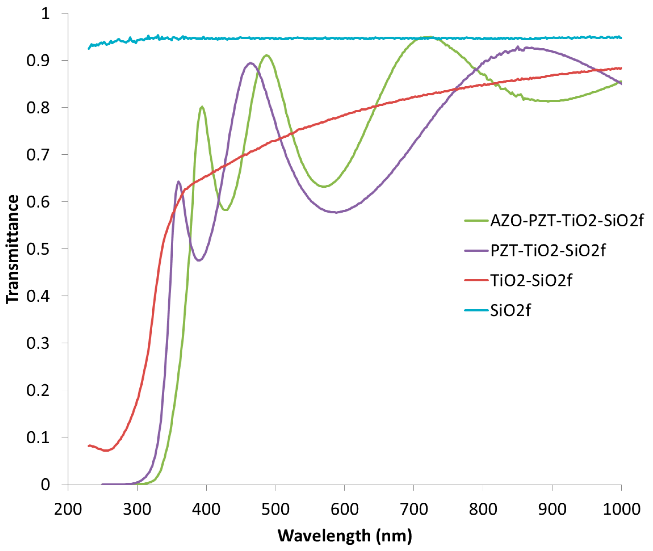
Figure 3.
Top-view optical micrograph of a final device showing patterned AZO IDE top electrodes. Here, the gap between subsequent fingers is 5 µm, and each finger is 5-µm-wide.
Figure 3.
Top-view optical micrograph of a final device showing patterned AZO IDE top electrodes. Here, the gap between subsequent fingers is 5 µm, and each finger is 5-µm-wide.

Figure 4.
Relative permittivity ε’ and tanδ at 1 kHz versus DC electric field E of a 7-tooth IDE structure with a 5 µm gap. Electrodes are made of (a) AZO and (b) Pt. For permittivity calculation, the stray capacitance was subtracted from the measured capacitance.
Figure 4.
Relative permittivity ε’ and tanδ at 1 kHz versus DC electric field E of a 7-tooth IDE structure with a 5 µm gap. Electrodes are made of (a) AZO and (b) Pt. For permittivity calculation, the stray capacitance was subtracted from the measured capacitance.
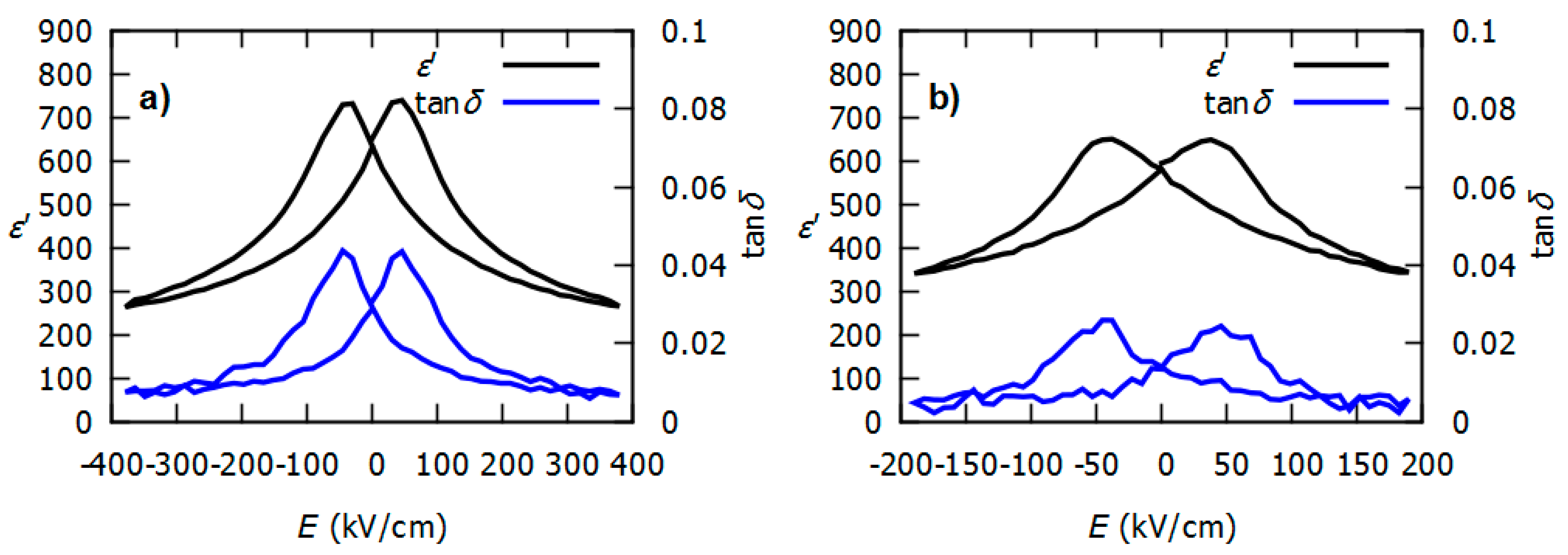
Figure 5.
Polarization-electric field (P-E) loop of the 200-nm PZT on glass with AZO 5-µm-gap IDE electrodes. The measurement was performed at 100 Hz.
Figure 5.
Polarization-electric field (P-E) loop of the 200-nm PZT on glass with AZO 5-µm-gap IDE electrodes. The measurement was performed at 100 Hz.

© 2017 by the authors. Licensee MDPI, Basel, Switzerland. This article is an open access article distributed under the terms and conditions of the Creative Commons Attribution (CC BY) license (http://creativecommons.org/licenses/by/4.0/).
Share and Cite
MDPI and ACS Style
Sette, D.; Girod, S.; Leturcq, R.; Glinsek, S.; Defay, E. Transparent Ferroelectric Capacitors on Glass. Micromachines 2017, 8, 313. https://doi.org/10.3390/mi8100313
AMA Style
Sette D, Girod S, Leturcq R, Glinsek S, Defay E. Transparent Ferroelectric Capacitors on Glass. Micromachines. 2017; 8(10):313. https://doi.org/10.3390/mi8100313
Chicago/Turabian StyleSette, Daniele, Stéphanie Girod, Renaud Leturcq, Sebastjan Glinsek, and Emmanuel Defay. 2017. "Transparent Ferroelectric Capacitors on Glass" Micromachines 8, no. 10: 313. https://doi.org/10.3390/mi8100313
Note that from the first issue of 2016, this journal uses article numbers instead of page numbers. See further details here.