1. Introduction
Microelectromechanical systems (MEMS) accelerometers are used in a wide range of markets and applications and can be classified in several categories: consumer grade, tactical grade and navigation grade depending on their performances, reliability and cost (see
Table 1) [
1,
2]. The consumer grade MEMS accelerometers are quite mature in consumer electronics and automotive electronics markets now [
3,
4], and are largely driven by lower cost, smaller size and multi-axis integration. On the contrary, the highest inertial navigation-grade markets are still dominated by macro electro-mechanical accelerometers such as Honeywell QA-3000 (Redmond, WA, USA) [
5], which can exhibit better than 1 ppm bias composite stability in one year.
With the development of MEMS technologies, MEMS accelerometers are penetrating more and more high-end applications such as aerial navigation, earthquake detection and gravity measurement [
6,
7,
8,
9]. Reduction in size of the sensing elements will offer many benefits, but also induce degradation of some specifications, such as measuring resolution, bias stability and the ratio of signal-to-noise. In general, unlike consumer grade accelerometers which are now using surface MEMS + CMOS (complementary metal-oxide-semiconductor) technology for their manufacturing [
10], high-precision MEMS accelerometers are still employing bulk silicon micromachining and hybrid assembly technologies [
11]. Many successful MEMS manufacturers are providing bulk silicon micro-machined capacitive accelerometers with highly symmetric beam-mass structures, such as Colibrys MS9000 (Neuchatel, Switzerland). Furthermore, the motion measurement of a free body needs to detect accelerations in three orthogonal directions. Common tactical grade MIMUs (Micro Inertial Measurement Units) on the market are orthogonally assembled by three individual and identical single-axis accelerometers on three different planes [
12,
13]. Thus, these MIMUs are suffering from the disadvantages of bulky package volume and possible assembly misalignment. To overcome these issues, the most effective way is to fabricate all three sensing elements on one single substrate, on the premise of not degrading any performances. There are many different reported approaches to fulfill this goal, such as by using a single proof mass but multiple electrodes for three-axis sensing [
14,
15], or by placing three sensing elements on a single die [
16,
17]. The first approach could realize extremely small size devices, but their performances are always limited by high cross-axis sensitivity. Then, the second approach normally uses comb finger sensing structures for in-plane acceleration measurement and sandwich structures for out-of-plane measurement. The combination of two different sensing structures allows a full optimization of each sensing structure’s performance, but it will also result in a much more complex fabrication process. Another possible solution using slanted-beam sensing structures was investigated in this paper, which employs very simple bulk silicon micromachining technologies and can also realize three-axis acceleration detection by fabricating four similar sensing elements on a single die.
In 1995, Andersson et al. firstly fabricated a micro-machined slanted-beam capacitive accelerometer with an asymmetrical structure [
18]. Later, in 2005, they extensively studied its working theory and performed device characterization at the Imego institute [
19,
20]. Because these accelerometers did not use differential detecting principles, their measured performances were quite limited. In addition, S. Butefisch et al. have also fabricated a glass-silicon-glass sandwich structure slanted-beam accelerometer aimed for a low-g sensor application [
21]. This sensing structure seems to be symmetrical, but because of the undercutting of silicon sidewalls during KOH etching, the fabricated proof mass can hardly ensure good symmetry. In capacitive accelerometers, it has been evidently demonstrated that accelerometers with highly symmetrical structures can exhibit much better performances [
7,
8,
9].
In this paper, a fully symmetrical slanted-beam accelerometer with all-silicon sandwich structures is presented. Its high symmetry is ensured by a specifically developed wet etch technique, and its all–silicon homogeneous structure can avoid the shortcomings of thermal coefficient mismatch and bring in chip-scale hermetic sealing. The fabricated prototype exhibits a good bias stability and low nonlinearity, experimentally demonstrating the effectiveness of our proposed design and fabrication technology.
2. Working Principles
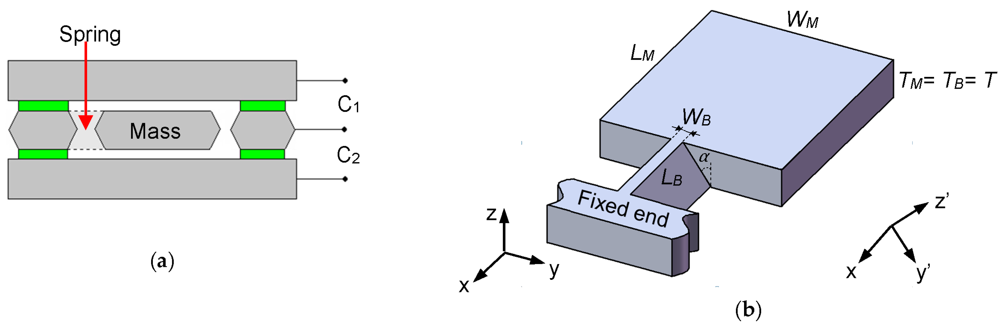
The working principles of this proposed accelerometer is based on a traditional differential capacitance detecting system, as shown in
Figure 1a. Its MEMS sensing part is composed of three different silicon layers, and the middle layer consists of a proof mass and a support spring that serve as the inertial sensing elements. When acceleration is applied, the proof mass will move upward or downward and cause a capacitance change (Δ
C =
C1 −
C2) that could be detected by the readout circuits. Then, the readout circuits will produce a voltage, and the change of this output voltage is proportional to applied acceleration.
The main difference of this slanted-beam accelerometer compared to ordinary spring-mass sensing structure is that its suspended beam is parallel to the {111} plane of a (100) silicon wafer (shown in
Figure 1b). Thus, its most sensitive direction is inclined to the wafer surface by an angle α = 35.3°, which is normally given by the crystal orientation of the monocrystalline silicon.
In order to simplify the analytical modeling, besides the normal coordinate system (x, y, z), another local coordinate system (x, y’, z’) is established with the z’-axis aligned normally to {111} the plane of the silicon crystal.
When an acceleration in the
z’-direction (
az‘) is applied on the sensing structure, the displacement and rotation of the outer tip of the supporting beam can be calculated by using the beam deflection theory [
22]. Its maximum displacement in the
z’ direction is:
The rotation angle of the proof mass around the
y’-axis is:
Here, geometrical parameters are outlined in
Figure 1b,
E is the Young’s modulus of silicon in (110) direction, and
I is the moment of inertia of the slanted beam:
F is the inertial force generated on the center of the proof mass:
Here, ρ is the density of silicon. Because capacitors are formed between two adjacent silicon wafers, only displacement of the proof mass in the
z-direction will bring changes in their capacitance values. When an acceleration in the
z’-direction is applied, the
z-axis displacement at any point of the proof mass (location is defined as
x) can be obtained as follows:
The calculation of sensitivity in the beam‘s stiffer direction, the
y’-axis, is analogous to the derivation process of Equation (5). The relationship between
dz,z’(x) and
dz,y’(x) is shown as below:
A readout circuit is used to detect the capacitances, and its output voltage is given by:
Here,
k is the total gain of the signal amplifier. Thus, the overall sensitivity of the accelerometer is:
Here,
a is the applied acceleration,
A0 is the plate area of each capacitor,
d0 is the original gap distance,
Δd is the average
z-axis displacement of the proof mass, and
ε is the permittivity of the gas in the gap. The sensitivity angle of the slanted-beam sensing structure can be calculated as follows:
Here, Sy and Sz represent the sensitivities of the slanted-beam accelerometer in the y- and z-directions, respectively.
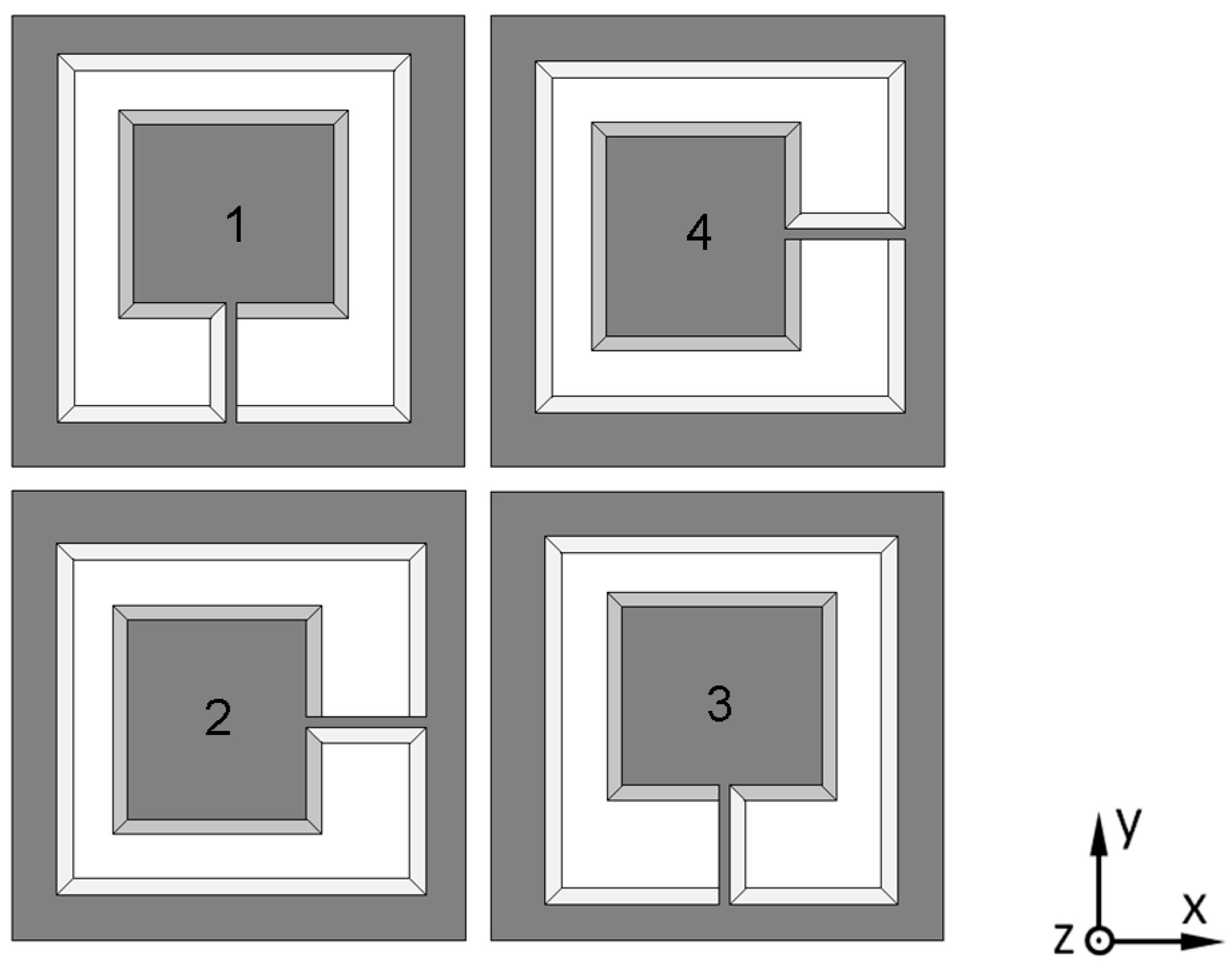
After analyzing the performance of one sensing structure, a three-axis design of the MEMS accelerometer is constituted by four of these sensing elements. As shown in
Figure 2, all of these sensing elements have the same geometrical parameters, and each one’s location is rotated by 90° in the arrangement.
Because each sensing element can detect accelerations in two orthogonal directions, four output signals related to three-axis accelerations could be obtained:
Here,
Si,j are the sensitivities in the
j-direction of sensing element
i, and
aj are the accelerations in the
j-direction. Then, a simple calculation needs to be performed after each measurement to separate three individual accelerations along the
x-,
y- and
z-directions:
3. Simulation and Structural Analysis
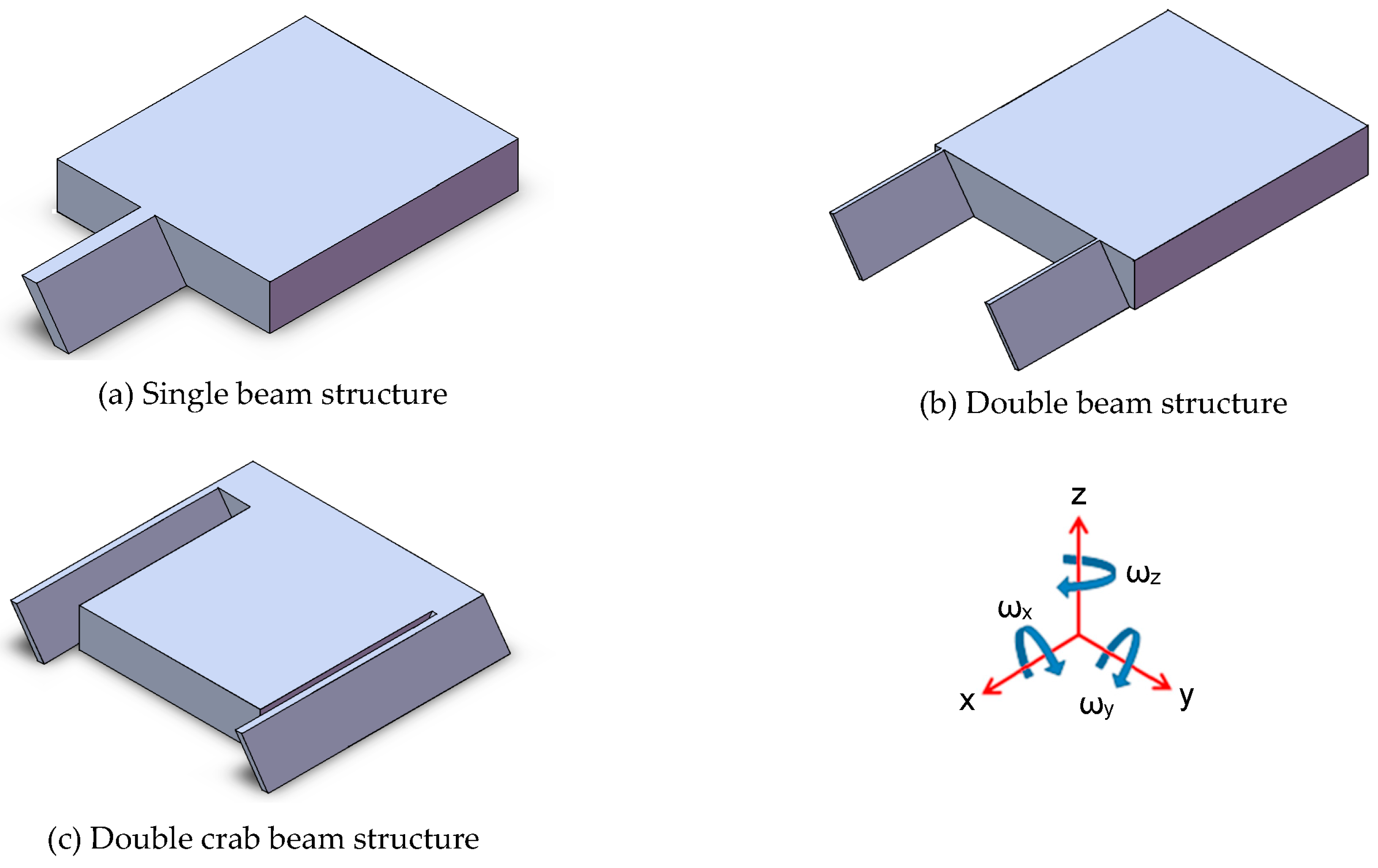
In the following content, three different simplified slanted beam-mass structures, as shown in
Figure 3, were analyzed by using a Finite Element Modeling (FEM) method and compared for their performances.
As they are not conventional spring-mass structures, potential rotation of the proof mass is a major concern at the initial design step. As shown in
Figure 3, ω
z rotation will not change the capacitance value, and ω
y rotation is a normal swing similar to the behavior of a traditional cantilever-type accelerometer; hence, only ω
x rotation is an unwanted movement. A comparison of these three structures, regarding their rotations under different directional applied accelerations, was performed. Geometrical parameters of our proposed design are given in
Table 2, and the comparative results are listed in
Table 3. What needs to be mentioned is that different dimensions of the slanted beams are used in this analysis in order to obtain similar output signal, which is given by the differential capacitance ratio: (
C1 −
C2)/(
C1 +
C2). As shown in
Table 3, all of these three structures exhibit extreme small ω
x rotation (ω
x ≤ 1.4 × 10
−5) when applied with 50 g acceleration, thus proving themselves good candidates for this inertial measurement.
Then, among them, a single beam mass structure was chosen for further investigation because of its geometrical simplicity, lower spring stiffness (considered for the same dimensions of the slanted beams) and internal stress relief of the whole beam mass structure.
Both analytical calculations and Finite Element Modeling (FEM) were performed to analyze this sensing element’s performance. The comparative results are shown in
Table 4. Because the two parallel plate method has neglected the capacitance fringe effects, the analytical calculation method gives a slight smaller value of initial capacitance value (
C0 = 16.7 pF) than the FEM method (
C0 = 16.8 pF). When a 50 g acceleration normal to the {111} plane is applied on the beam mass structure, the proof mass will move 0.136–0.667 μm in the
z-direction, which brings in a capacitance change of 7.15 pF and a differential ratio of 0.202. Then, the device’s sensitivity angle was calculated by using both Equation (9) and FEM methods, and the two results are, as expected, both larger than the silicon crystal orientation 35.3°. The dynamic analysis of this sensing element was also performed. The first resonance mode of this structure corresponds to a vibration normal to the {111} plane of the slanted supporting beam, and its resonance frequency is 3.9 kHz. The second resonance mode corresponds to the undesired roll rotation with a resonance frequency of 16 kHz. Since the natural frequency of the first mode is much smaller than higher modes, the sensor’s sensing mode proves to be successfully decoupled from other unwanted vibration modes.
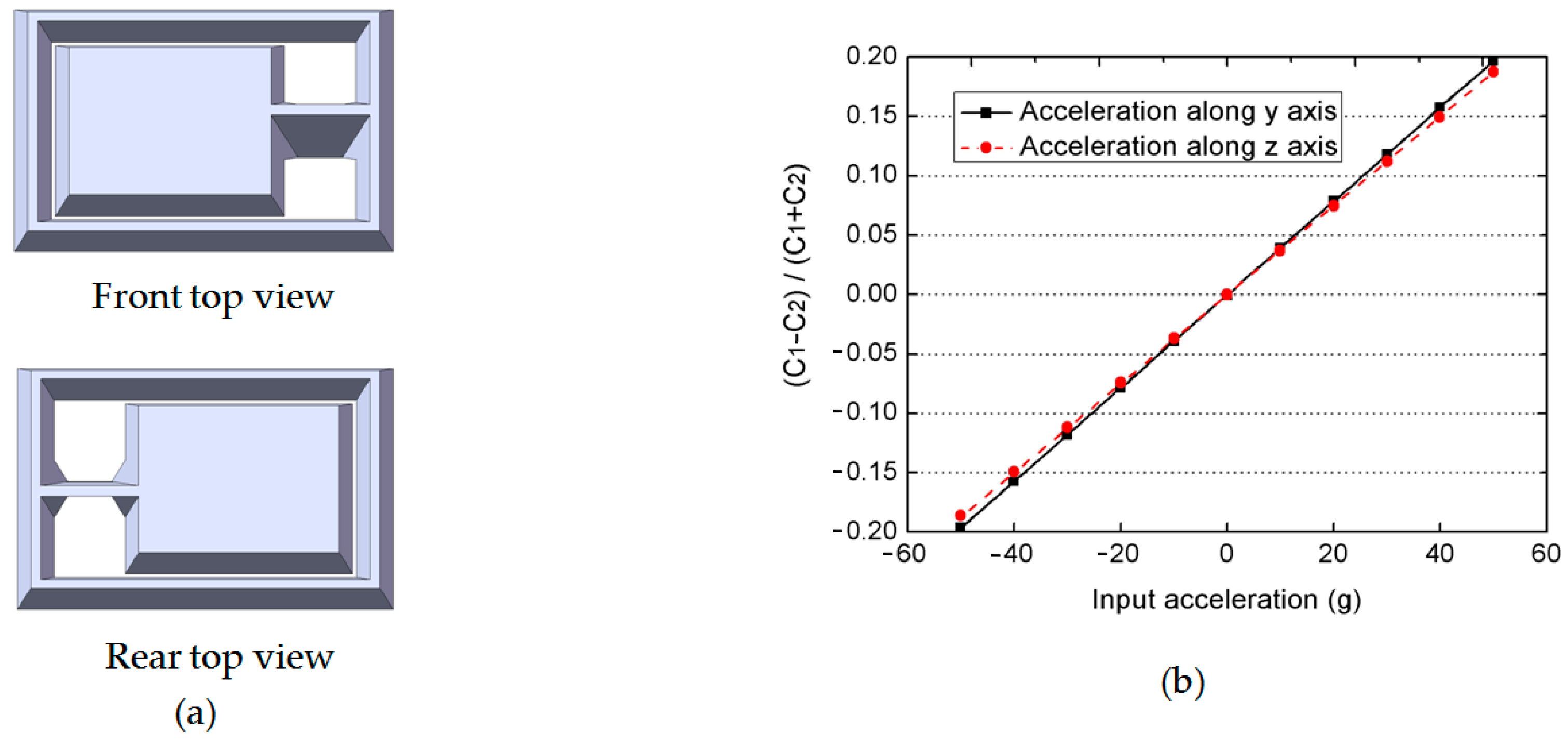
Since former analysis is only based on simplified models, a more accurate 3D model is established to simulate the performance of the real fabricated devices. As shown in
Figure 4a, convex corners will be formed at both ends of the slanted supporting beam because of the etching properties of the chosen wet etchant.
Simulated output signals (differential capacitance ratio: (
C1 −
C2)/(
C1 +
C2)) as a function of applied accelerations in both the y- and z-axes are plotted in
Figure 4b. These two lines show very good linearity (nonlinearity: 0.35‰ on the
y-axis and 0.45% on the
z-axis) over a sensing range up to ±50 g, and the sensitivities in two orthogonal directions only have a very small difference (
ky = 3.93 × 10
−3,
kz = 3.75 × 10
−3). Its sensitive angle could then be calculated to be 43.7°.
Another issue about this accelerometer is the influence of its parasitic capacitance. Since it has a rigid outer frame (frame width = 50 am) to a protect central sensitive area, large parasitic capacitance (≈10.5 pF) is generated from the bonding SiO
2 area and may worsen the accelerometer’s nonlinearity performance. This effect is eliminated by the readout circuit design. Actually, a more detailed transfer function of the detecting circuit is expressed as:
Here, C1 and C2 are variable capacitances of the upper and lower capacitor, Cpi are their parasitic capacitances, Ccomp is a programmable compensation capacitance integrated in the front end C-V converter. This slanted-beam accelerometer has a very good symmetry to ensure Cp1 = Cp2. Then, by adjusting the programmable compensation capacitance Ccomp, the sum of Cp1 and Cp2 can be subtracted in this transfer function.
4. Device Fabrication
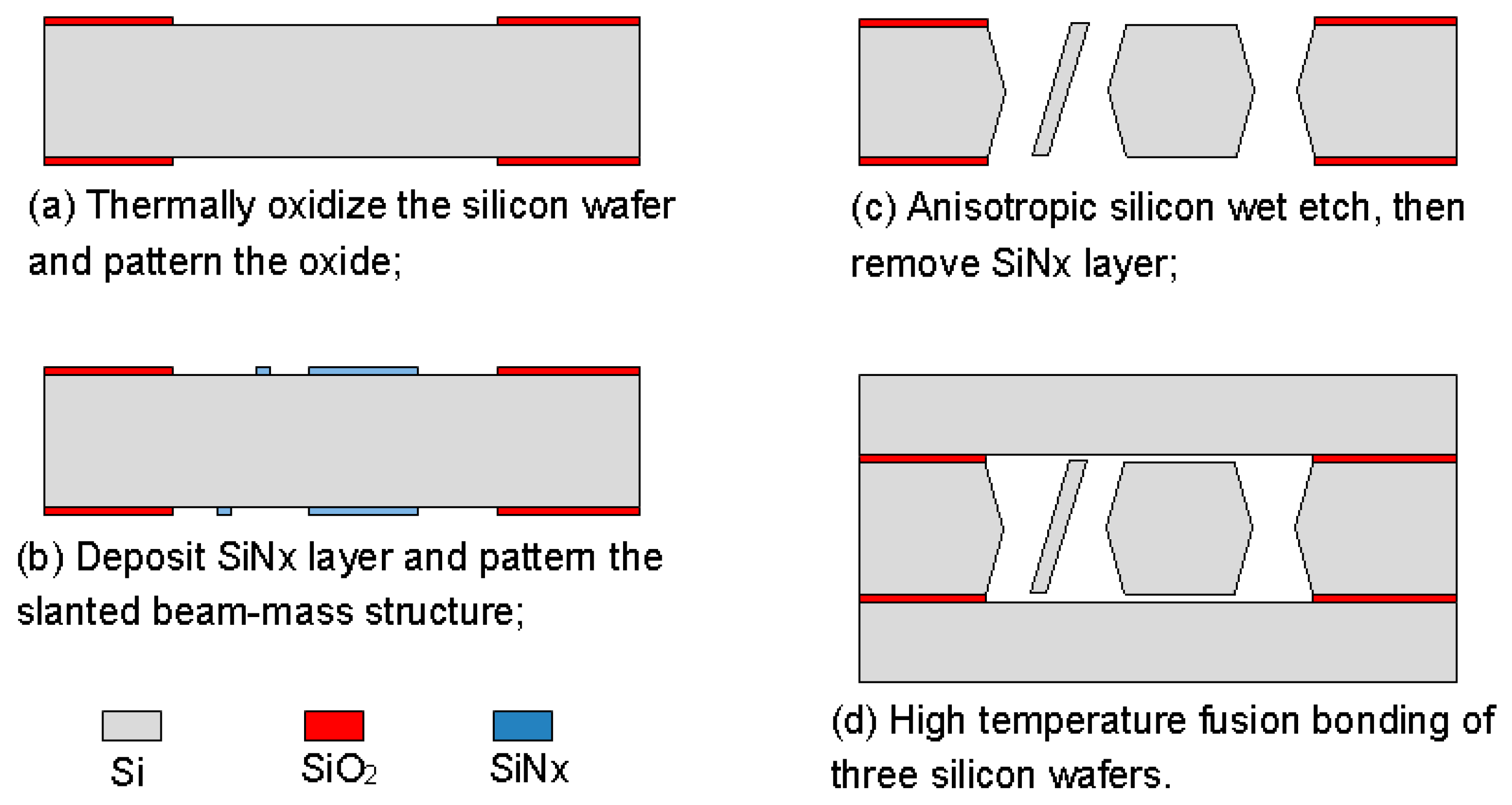
The proposed fabrication process flow of the single slanted-beam accelerometer is briefly outlined in
Figure 5. Firstly, a double side polished silicon wafer (4 inch, thickness 380 μm, (100) orientation, resistivity 0.1 Ω·cm) is thermally oxidized to grow 2 μm SiO
2 on its two surfaces at 1100 °C. Subsequently, the two oxide layers are patterned by using double-sided mask aligner and BHF (Buffered Hydrofluoric Acid) etch (
Figure 5a). These oxide layers serve as electrical isolation and define the initial distance of capacitance gap. Next, the whole silicon wafer is deposited by a 600 nm SiN
x layer on both of its sides (
Figure 5b), and these SiN
x layers are patterned to form the etching mask of the slanted beam-mass sensing structure. The silicon wafer is then etched in wet anisotropic etching solution until the slanted beam is successfully formed (
Figure 5c). This structured silicon wafer and two other silicon wafers are hermitically sealed by using a high temperature Silicon Fusion Bonding (SFB) process (
Figure 5d). Finally, a film of Cr/Au is simultaneously evaporated on three different layers to define the contacts’ metallization.
The wet etch process is performed with 25 wt % TMAH (Tetramethylammonium Hydroxide) + 0.1% (
v/
v) Triton-X-100 [C
14H
22O(C
2H
4O)
n,
n = 9–10] solution. A constant temperature bath at 80 °C is used to keep the etchant temperature within ±1 °C. Our formerly reported results [
7] have already demonstrated that additive-modified TMAH could provide the minimum undercutting at the mass corner. However, this time, the wet etch process needs a much longer time than etching through the wafer. According to our experiences, the effect of additive has already reached its limit and can no longer be competent for this task. Thus, a specific wet etching technique is developed mainly based on designing a compensation pattern in the masking layer and combining it with an additive-modified solution. Different stages of the technical development and their corresponding fabricated results are shown in
Table 5. As we can see, after adding both the additive solvent and a ‘T’ shape compensation structure (
d = 10 μm,
l = 40 μm), a well protected convex corner is successfully fabricated.
Then, this middle silicon wafer is bonded with two other silicon wafers to form the differential capacitors. Care must be taken about the cleaning of the bonding surface prior to the temporal Si-SiO
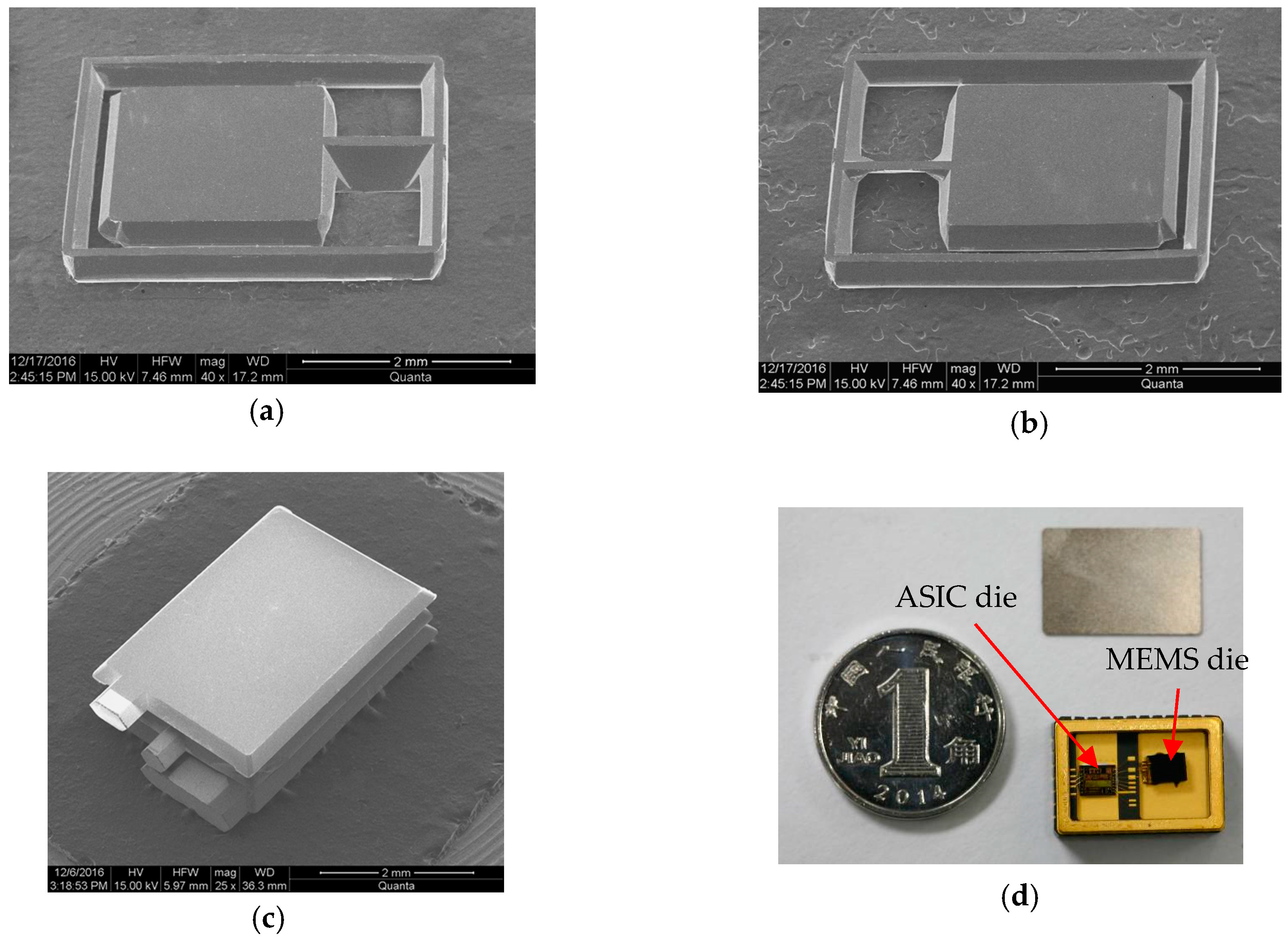
2 bonding. A high temperature annealing (>1000 °C) for 2 h is needed to permanently seal the cavity. After these process steps, a slanted-beam MEMS die with a highly symmetrical spring-mass structure has been fabricated.
Figure 6a,b show the front side and back side SEM images of fabricated single slanted beam-mass structure, and
Figure 6c shows the bonded three-layer device. Thereafter, the MEMS die is diced and assembled with a proprietary Application Specific Integrated Circuit (ASIC) die in a hermetically sealed Multichip Module (MCM) as shown in
Figure 6d.
5. Measurement Results
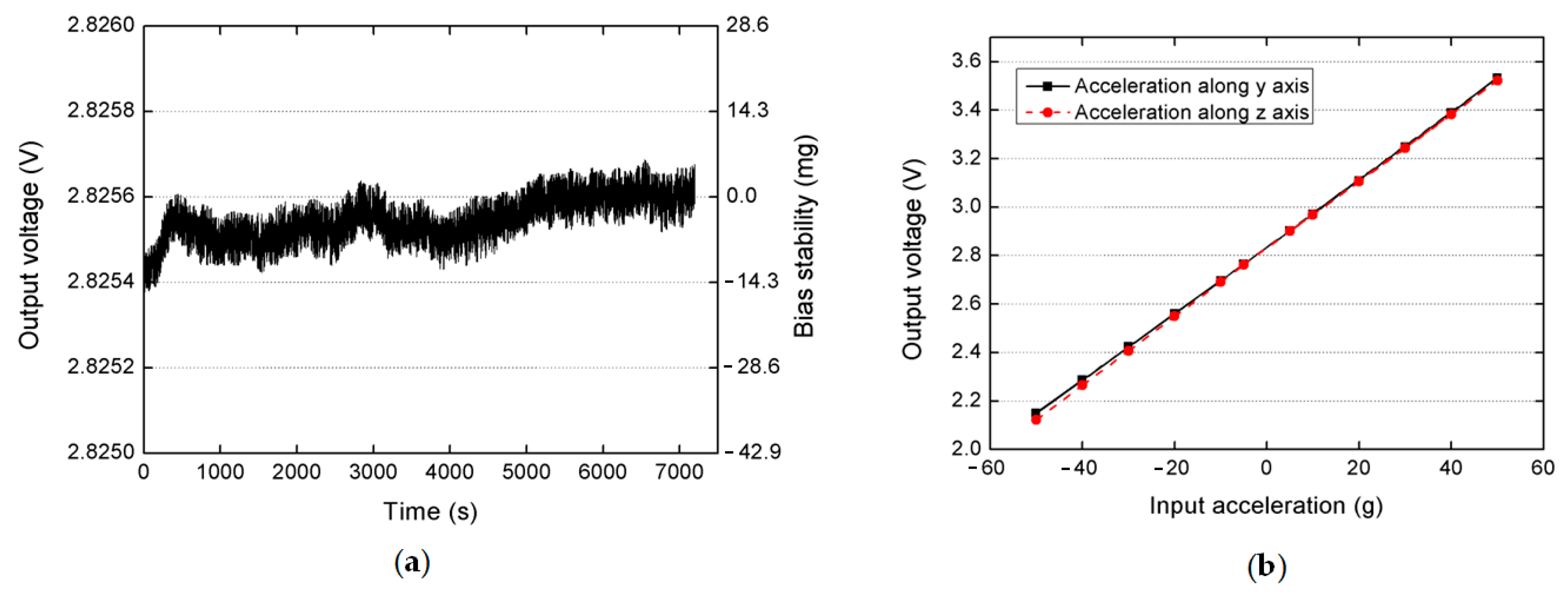
A preliminary test was performed to validate the effectiveness of a fabricated slanted-beam accelerometer. The bias stability performance was measured at room temperature for 12 min without any compensation. Its output signal was recorded immediately after the power was turned on, and the result in
Figure 7a shows that this accelerometer has demonstrated a short-time bias stability of 3.84 mg (1σ) or 15.7 mg (maximum drift). The white noise of this accelerometer was also measured to be 40.2 μV/√Hz. Then, the accelerometer’s dynamic response was also measured by using a precise centrifuge in the range of ±50 g. The plots in
Figure 7b show that the accelerometer almost has a similar scale factor in two orthogonal directions (13.79 mV/g on the
y-axis and 13.98 mV/g on the
z-axis), and its nonlinearity in two directions are both smaller than 0.5% (0.48% on the
y-axis and 0.49% on the
z-axis). The sensitivity angle is calculated to be 45.4°, which is larger than simulated value 43.7°. This difference results from the geometrical errors of fabricated slanted beams and could be minimized by future optimization of the fabrication processes. A comparison of FEM values and measured values of this prototype are listed in
Table 6.
Table 7 shows the comparison of some recently reported capacitive MEMS accelerometers with the slanted-beam accelerometer fabricated in this work. It can be seen that this accelerometer needs very simple bulk silicon fabrication processes, while also achieving good performance. These measured results demonstrate the effectiveness of our proposed design and fabrication technology. Since this prototype only used open loop control ASIC, a close loop circuit is under consideration to achieve better nonlinearity and lower noise.


