
Array Multipliers for High Throughput in Xilinx FPGAs with 6-Input LUTs †

Penn State Erie, The Behrend College, Department of Electrical and Computer Engineering, 5101 Jordan Road, Erie, PA 16563, USA
†
This paper is an extended version of our paper published in Walters III, E.G. Partial-Product Generation and Addition for Multiplication in FPGAsWith 6-Input LUTs. In Proceedings of the 48th Asilomar Conference on Signals, Systems, and Computers, Pacific Grove, CA, USA, 2–5 November 2014; pp. 1247–1251.
Computers 2016, 5(4), 20; https://doi.org/10.3390/computers5040020
Submission received: 19 June 2016
/
Revised: 13 September 2016
/
Accepted: 18 September 2016
/
Published: 23 September 2016
Abstract
:Multiplication is the dominant operation for many applications implemented on field-programmable gate arrays (FPGAs). Although most current FPGA families have embedded hard multipliers, soft multipliers using lookup tables (LUTs) in the logic fabric remain important. This paper presents a novel two-operand addition circuit (patent pending) that combines radix-4 partial-product generation with addition and shows how it can be used to implement two’s-complement array multipliers. The circuit is specific to modern Xilinx FPGAs that are based on a 6-input LUT architecture. Proposed pipelined multipliers use 42%–52% fewer LUTs, and some versions can be clocked up to 23% faster than delay-optimized LogiCORE IP multipliers. This allows 1.72–2.10-times as many multipliers to be implemented in the same logic fabric and potentially offers 1.86–2.58-times the throughput by increasing the clock frequency.
1. Introduction
Field-programmable gate arrays (FPGAs) are often used in signal processing systems for many applications, such as digital-signal processing (DSP), video processing and image processing. For these applications and others, computation of a sum-of-products is very common. As a result, multiplication is often the focus of efforts to reduce required resources, delay and power. For this reason, most contemporary FPGAs have embedded hard multipliers distributed throughout the fabric. Even so, soft multipliers using lookup tables (LUTs) in the configurable logic fabric remain important for high-performance designs for several reasons:
- Flexible size and type: Embedded multiplier operands are fixed in size and type, e.g., two’s complement, while LUT-based multiplier operands can be any size or type.
- Flexible placement: The number and location of embedded multipliers are fixed, while LUT-based multipliers can be placed anywhere, and the number is limited only by the size of the reconfigurable fabric.
- Hybrids: LUT-based multipliers are often combined with embedded multipliers to make larger multipliers.
Parandeh-Afshar and Ienne discuss the importance of this topic and present techniques to improve the performance of soft multipliers in Altera FPGAs [7]. They present radix-2 Baugh–Wooley multipliers and radix-4-modified Booth multipliers that use generalized parallel counters (GPCs) in the logic fabric to reduce the partial-product matrix to two or three rows, which are then added using a carry-propagate adder (CPA). This builds on the previous work of Parandeh-Afshar et al. using GPCs for compressor trees for the more general case of multi-operand addition [8,9,10]. In other work, Parandeh-Afshar et al. suggest modifications to the FPGA logic fabric to improve soft multiplier implementations [11,12]. Matsunaga et al. have also published work on using GPCs for multi-operand addition [13,14,15]. De Dinechin and Pasca present methods for implementing large multipliers and squarers on Xilinx FPGAs using a combination of embedded multipliers and logic-based multipliers [16]. Gao et al. present a method for implementing large multipliers that combine embedded multipliers with GPCs [17]. Brunie et al. model a generalized weighted sum of bits as a bit heap and describe techniques for summing them using a combination of embedded multipliers and GPCs on Altera and Xilinx FPGAs [18]. Kumm and Zipf present novel GPCs for Xilinx FPGAs and use them with integer linear programming (ILP) in compressor trees [19]. Mhaidat and Hamzah compare the use of GPCs to Wallace and Dadda multipliers [20]. Kumm et al. use a method similar to this work to implement softcore multipliers [21].
Unlike much of the related work, this paper is specific to the Xilinx 6-input LUT architecture found in the Spartan-6, Virtex-5, Virtex-6, 7-Series, UltraScale and perhaps future generations. The underlying generate-add unit (patent pending) can be used for many purposes, but this paper focuses on its use in general-purpose array multipliers. Previous work describes a radix-4 partial-product generate-add structure and shows how it can be used to make array and tree multipliers [22,23,24]. This paper extends that work in several ways:
- The generate-add unit is described in greater detail, and new optimizations are presented.
- Proposed array multipliers are described in greater detail, and new optimizations are presented.
- All new synthesis results are given using Vivado instead of the ISE toolchain; LogiCORE IP v12.0 multipliers are compared instead of v11.2; and more operand sizes are synthesized.
The new optimizations further reduce the number of required LUTs by approximately 10% and provide approximately a 1.5-times speedup compared to [22]. The proposed multipliers are believed to be the only designs to date that produce better results than LogiCORE IP LUT-based multipliers.
The paper is organized as follows. Section 2 gives background information. Section 3 discusses related work using GPCs. Section 4 describes the proposed two-operand adder, and Section 5 describes the proposed LUT-based array multipliers. Synthesis results are discussed in Section 6, and conclusions are given in Section 7.
2. Background
This section describes the details of the Xilinx logic fabric, two-operand addition in the Xilinx logic fabric, Altera logic fabric and radix-4-modified Booth multiplication.
2.1. Xilinx Logic Fabric
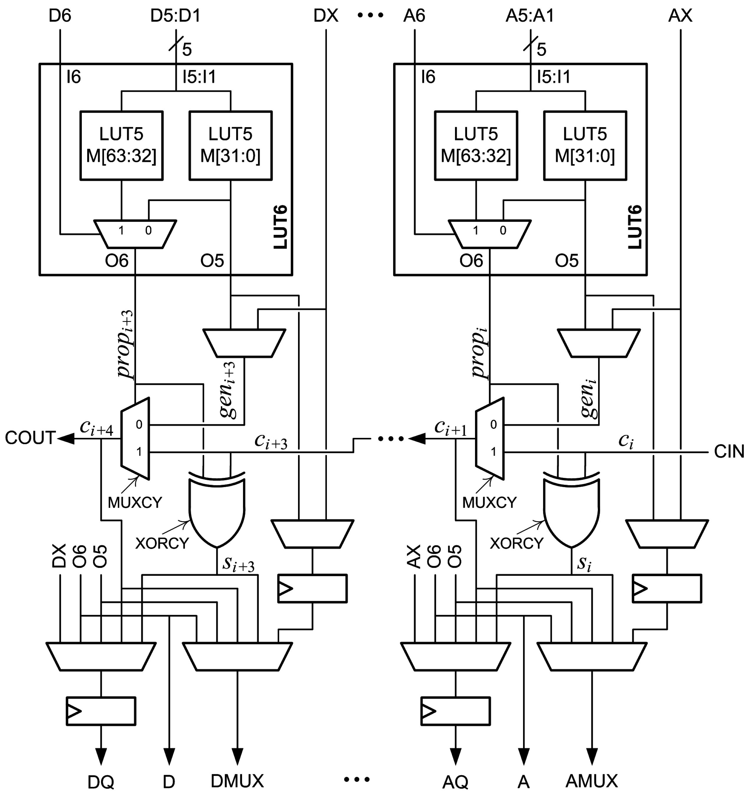
The main logic resource for implementing combinational and sequential circuits in a Xilinx FPGA is the configurable logic block (CLB). Each CLB has two slices. Figure 1 is a partial diagram of a 7-Series FPGA slice. Each slice has four 6-input lookup tables (LUT6s) designated A, B, C and D. Each LUT6 is composed of two 5-input lookup tables (LUT5s) and a two-to-one multiplexer. The two LUT5s are memories that share five inputs designated I5:I1. The memory values are designated M[63:32] in one LUT5 and M[31:0] in the other LUT5. The output of the M[31:0] LUT5 is designated O5. The sixth input, I6, is input to a multiplexer that selects one of the LUT5 outputs. The selected output is designated O6. The LUT6 is normally configured as either two LUT5s with five shared inputs and two outputs by connecting I6 to logic “1”, or as one LUT6 with six inputs and one output by connecting I6 to the sixth input [25,26].
A multiplexer and an XOR gate, indicated in Figure 1 as MUXCY and XORCY respectively, are associated with each LUT6. Inputs to the MUXCY associated with the A LUT6 are a select signal, , a first data input, , and a second data input, . The output of the MUXCY, , is connected to the MUXCY associated with the B LUT6. These connections continue through the C and D LUT6s to form a fast carry chain within the slice. The output of the slice, COUT, can be connected to the input of the next slice, CIN, to form longer carry chains. The signal is driven by the O6 output of the corresponding LUT6. The signal is selected by a configuration multiplexer and is either the O5 output of the corresponding LUT6 or the bypass input, which is designated AX, BX, CX or DX. The fast carry logic in a slice, which includes four MUXCYs, four XORCYs and the fast carry chain, is called a CARRY4 [26].
Two flip-flops are associated with each LUT6. One flip-flop can be used to register O5 or the bypass input. The other flip-flop can be used to register O5, O6, the bypass input, the MUXCY output or the XORCY output.
The Spartan-6, Virtex-5, Virtex-6 and UltraScale families are similar to the 7-Series. One notable difference is that the Spartan-6 family does not have fast carry chains in every column of slices.
2.2. Two-Operand Addition
Suppose X and Y are to be added using the Xilinx fast carry logic. For the i-th column of the adder, and are the bits of X and Y, respectively; is the carry-in bit; is the carry-out bit; and is the sum bit. A truth table can be made for the adder; then, required values for and can be derived from the table.
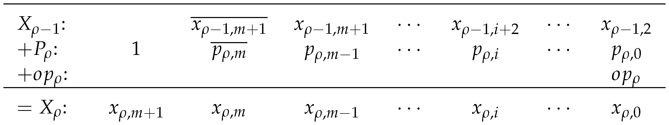
Figure 1 shows that , so must have the same value as to produce the correct value for the sum bit. When , the generate signal becomes the carry out, so must have the same value as the expected value of . When , the generate signal is not used, so it is a don’t-care. These values are given in Table 1. Next, and are expressed as functions of and . Inspection of the truth table shows that and that the generate signal can be either or .
2.3. Altera Logic Fabric
The multipliers proposed in this paper are specific to the Xilinx LUT6 architecture and are not applicable to Altera FPGAs. The Altera logic fabric is briefly described here to give context to related work on generalized parallel counters (GPCs).
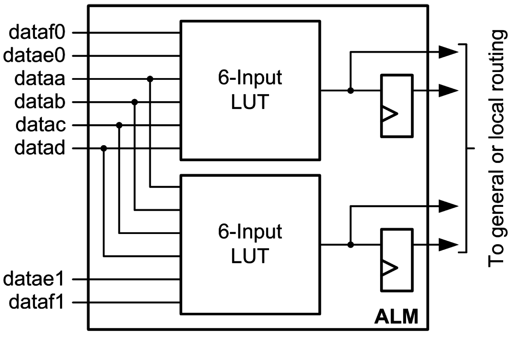
The main logic resource for implementing combinational and sequential circuits in an Altera Stratix V FPGA is the logic array block (LAB) [27]. Each LAB in the Stratix V has ten adaptive logic modules (ALMs). The ALM has evolved, but the general functionality described in this section applies to the older Stratix II family [28] through the latest family, the Stratix 10 [29].
The capabilities of an ALM can be compared to a Xilinx LUT6 and its associated MUXCY, XORCY and flip-flops. An ALM can be configured to implement two functions of six inputs, provided that four of the inputs are common, as shown in Figure 2. By comparison, a Xilinx LUT6 can implement one function of six inputs or two functions of five shared inputs.
Each ALM includes two full adders and dedicated carry connections to implement fast addition. Figure 3 shows an Altera ALM in arithmetic mode.
2.4. Radix-4-Modified Booth Multipliers
Suppose A and B are to be multiplied. If the multiplicand, A, is an m-bit two’s-complement integer and the multiplier, B, is an n-bit two’s-complement integer, then:
MacSorley’s modified Booth recoding algorithm works for both unsigned and two’s-complement multipliers [30]. First, is concatenated to the right of B and set to “0”. For two’s-complement multipliers, n must be even. If it is not, B is sign extended by one bit to make n even. For unsigned multipliers with odd values of n, B is zero-extended with one “0” to make n even. If n is already even, B is zero-extended with two “0”s.
Next, B is recoded two bits at a time using overlapping groups of three bits. For each , , and are recoded as a radix-4 signed digit, , where and . Each partial product, , is . Digit recoding and partial-product selection are summarized in Table 2. Finally, the product is computed as:
If a partial product is , then the multiplicand, A, is selected. If a partial product is , then the multiplicand is shifted left one bit before selection. If a partial product is or , then A or is subtracted by complementing each bit and adding “1” to the least significant bit (LSB). Table 3 summarizes partial-product generation for each selection. There are bits in the partial product to provide for a left shift of A, with sign extension if A is not shifted. The operation bit, , is set to “0” for addition or “1” for subtraction and is added to the LSB column of the partial product.
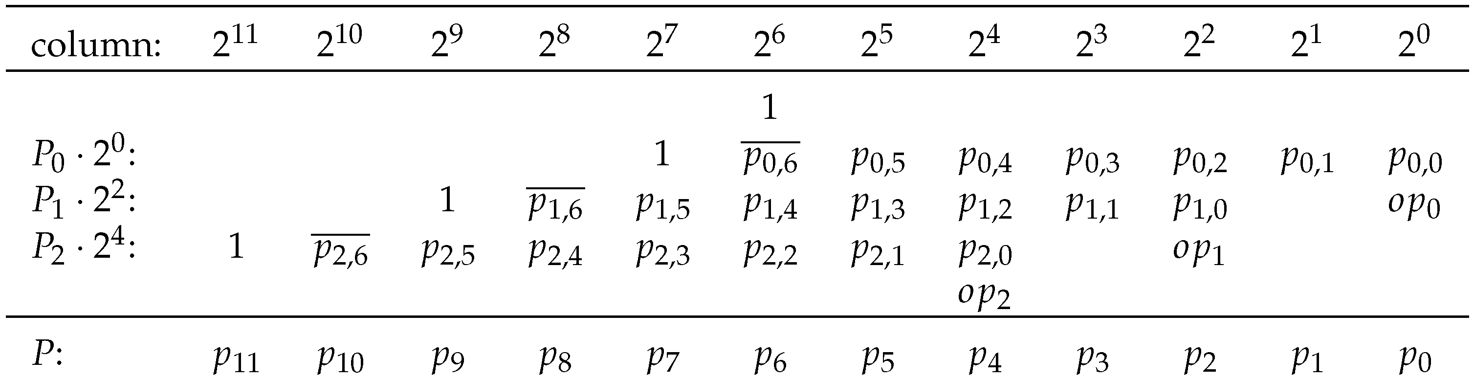
Each partial product is sign extended to the width of the multiplier in order to provide for correct addition and subtraction. Sign extension can be accomplished by complementing the sign bit, adding a “1” in the same column, and extending with constant “1”s. The constants are pre-added to reduce the number of “1”s in the matrix. Figure 4 shows the simplified partial-product matrix for a multiplier [31,32,33].
3. Related Work: Generalized Parallel Counters
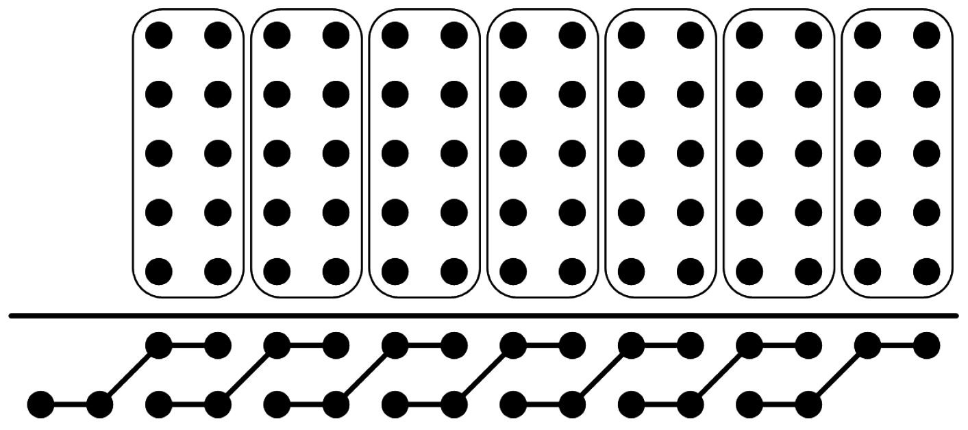
The well-known Wallace tree [34] and Dadda [35] multipliers use full adders and half adders to reduce the partial-product matrix to two rows, which are then added using a final CPA. A full adder is sometimes called a (3;2) counter, because it adds three bits in the same column and outputs a two-bit result equal to the sum of the three bits. A GPC adds bits in one or more columns and produces an n-bit result equal to the sum of the bits, taking into account the weight of the columns [36]. For example, a (5,5;4) counter adds five bits in the column and five bits in the column and outputs a four-bit result equal to the weighted sum of the ten input bits. Figure 5 shows how several (5,5;4) counters could be used to reduce five rows of bits to two rows.
Parandeh-Afshar et al. are believed to be the first to look at using GPCs implemented using LUTs to build compressor trees for multi-operand addition in FPGAs [8,9,10]. They note that modern FPGAs, such as Altera Stratix II and newer and Xilinx Virtex-5 and newer, have 6-input LUTs. Therefore, they focus on GPCs that have up to six total inputs for efficient usage of the LUTs and show that (6;3), (1,5;3), (2,3;3) and (3,3;4) counters each map to two ALMs in modern Altera FPGAs. They use a heuristic to implement multi-operand adder compressor trees with GPCs in [8], use integer linear programming (ILP) to improve the results in [9] and improve the GPCs themselves by using the ALM fast addition resources in [10]. They note that both Altera and Xilinx have efficient ternary adders, so they use GPCs to reduce the matrix to three rows. Other work on GPCs that is based on work by Parandeh-Afshar et al. presents incremental improvements or additional applications for GPCs [13,14,15,17,20]. Kumm and Zipf present two novel GPCs, (6,0,6;5) and (1,3,2,5;5), that are specific to and optimized for Xilinx FPGAs [19].
4. Proposed Two-Operand Adder
Suppose X and Y are to be added using the Xilinx fast carry logic. For the i-th column of the adder, and are the bits of X and Y, respectively; is the carry-in bit; is the carry-out ; and is the sum bit. The signal must be set to , and the signal can be set to either or to add and [22]. If and together are a function of five or fewer inputs, then the LUT6 can be configured as two LUT5s, generating either or at O5, routing it to and generating at O6 to drive . If and together are a function of six inputs, then the LUT6 can be configured to generate at O6 to drive and or can be applied to the bypass input and configured to drive the input. A disadvantage of this configuration is that the bypass flip-flop cannot be used.
Normally, a LUT6 can be used to either generate a function of six inputs at O6 or to generate two functions of five inputs at O5 and O6 [25,26]. However, there are several useful cases where one function of six variables can be output at O6 and a separate function of five shared variables can be output at O5. Suppose is a function of one variable connected to I6 and is a function of five variables connected to I5:I1. The function is stored in M[31:0], so is output at O5. If is “0”, is also output at O6. If is “1”, the function stored in M[63:32] is output at O6. If is stored in M[63:32], then is generated at O6 and is generated at O5. This can be used to add and without using the bypass input when is a function of one variable and is a function of up to five variables. Figure 6 shows the connections for this configuration. This frees the bypass input to be connected to the bypass flip-flop to implement additional registers. Input I6 has the shortest delay path, and I1 has the longest [25], so this method also allows faster inputs to be used if is a function of less than five variables. The carry into the proposed adder, , can be used to implement subtraction or to add an extra bit to the least significant column.
5. Proposed Multipliers
This section describes how the proposed array multipliers are implemented and pipelined.
5.1. Partial-Product Selection and Generation
MacSorley’s algorithm adds zero when by generating and setting . In the proposed multiplier, is generated, and is set to “1”. This complements each bit in and adds “1” to subtract zero [32]. With this modification, the operation bit , as opposed to MacSorley’s algorithm where is a function of three variables. This eliminates the logic resources and additional delay required to generate and simplifies the layout on the FPGA fabric. Table 4 shows the proposed partial-product selection (cf. Table 2), and Table 5 shows the proposed partial-product generation (cf. Table 3).
5.2. Combined Partial-Product Generation and Addition
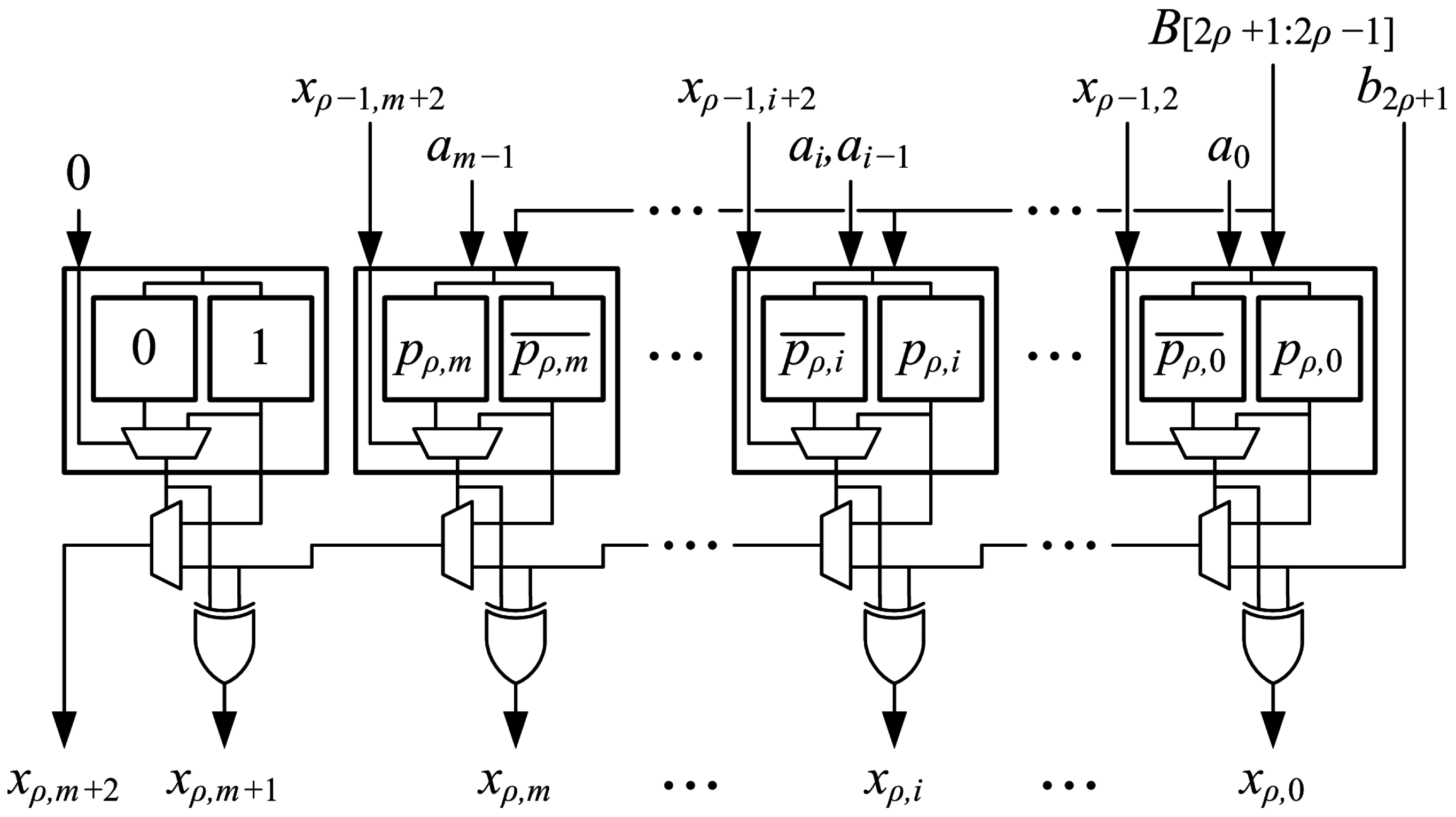
Partial-product generation and addition of a second value are combined into a generate-add unit, which is the main building block of the proposed array multipliers. The arithmetic operation is shown in Figure 7. Each unit generates one radix-4 partial product, , with a leading “1” and the most-significant bit (MSB) complemented to implement sign extension. The operation bit, , and the MSBs of the output from the previous generate-add unit, , are added to produce an accumulated sum, . The two LSBs of are bits and of the final product, so they are not added in the next unit. The generate-add unit is shown in Figure 8. It is implemented using an -bit proposed two-operand adder as described in Section 4, with and as the X and Y addends, respectively.
Bit i of partial product , , is a function of five inputs:
The inputs for each bit, , are connected to the I5:I1 inputs of a LUT6. is connected to I6 of the same LUT6. The M[31:0] LUT5 is configured to generate , and the M[63:32] LUT5 is configured to generate . O6 then generates and drives . O5 generates and is selected to drive . This is done for all of the partial-product bits except the MSB, . The MSB is complemented for sign extension by generating in the M[31:0] LUT5 and in the the M[63:32] LUT5. O6 then generates and drives . O5 generates and is selected to drive . The leading “1”, , is added by configuring the M[31:0] LUT5 to generate “1”, configuring the M[63:32] LUT5 to generate “0” and wiring “0” to I6, so that and . To summarize, the M[31:0] LUT5s generate the bits of ; the M[63:32] LUT5s generate the complement of those bits; and the bits of to be added are wired to the I6 inputs. The operation bit, , is added by wiring to . The sum produced at the XORCY output is , which is added to in the next generate-add unit.
Table 6 is the truth table for a LUT6 that generates the partial product and adds it to the bit input to I6, e.g., . Note that the values for O6 are stored in M[63:32], and the values for O5 are stored in M[31:0].
5.3. Optimizations for the Generate-Add Unit
The most-significant LUT, shown in Figure 8, can be simplified and eliminated. Inspection of the circuit shows that the input to the MUXCY is always “1”. This means that the input to the MUXCY is never used, so it is a don’t-care. This could be implemented by storing all “1”s in the M[63:32] LUT5 and wiring “1” to the I6 input, which frees the M[31:0] LUT5 to be used for another purpose. When this is done, the Xilinx tools optimize the entire LUT6 away. The Verilog models used in this work simply assign “1” to the input of the CARRY4 primitive.
Pipelined array multipliers reported in previous work [22] had an interesting result for delay. multipliers were slower than multipliers (2.402 ns vs. 2.144 ns), and multipliers were slower than multipliers (2.471 ns vs. 2.160 ns). These multipliers were implemented using the generate-add structure shown in Figure 8, which requires LUT6s. When is a multiple of four, slices are fully utilized. Inspection of Figure 1 shows that the XORCY output and the MUXCY output are registered using the same flip-flop. When is a multiple of four, such as for and multipliers, the output from the MUXCY cannot be registered within the same slice because the output and the other XORCY outputs use all of the available flip-flops. This forces to be routed outside of the slice to an available flip-flop, causing the additional delay due to longer and slower interconnect.
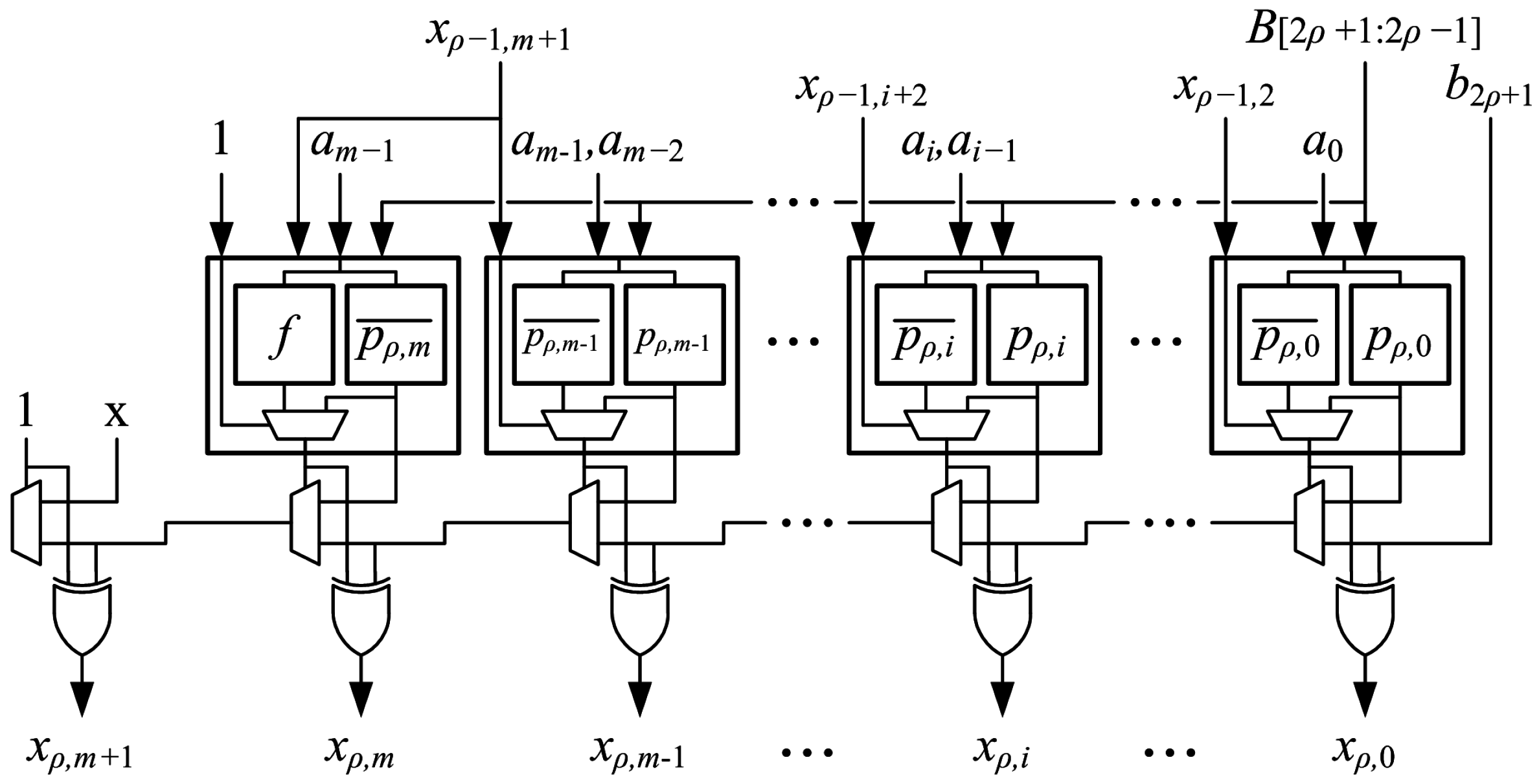
This problem is avoided by noting that . The output is used in the next row instead of so that the MUXCY output does not need to be registered. Figure 9 shows the arithmetic that is performed (cf. Figure 7). The optimized generate-add unit generates with a leading “1” and the MSB complemented to implement sign extension as in the original generate-add unit. The operation bit, , and the () MSBs of , using instead of , are added to produce an accumulated sum, . The MSB of the output, , is not needed in the next row, so it is not produced.
The most-significant LUT6 of the optimized generate-add unit is configured differently than the other LUT6s. The MSB from the previous unit, , is connected to one of the shared I5:I1 inputs, and “1” is input to I6. The M[31:0] LUT5 is configured to produce at O5 to drive the signal. The M[63:32] LUT5 is configured to produce the function at O6 to drive the signal. Since ,
Table 7 gives the truth table the for the most-significant LUT6 of an optimized generate-add unit.
Figure 10 shows the optimized generate-add unit. The optimized generate-add unit uses only LUT6s and avoids the delay of routing a MUXCY output out of a slice to be registered.
5.4. Array Structure and Pipelining
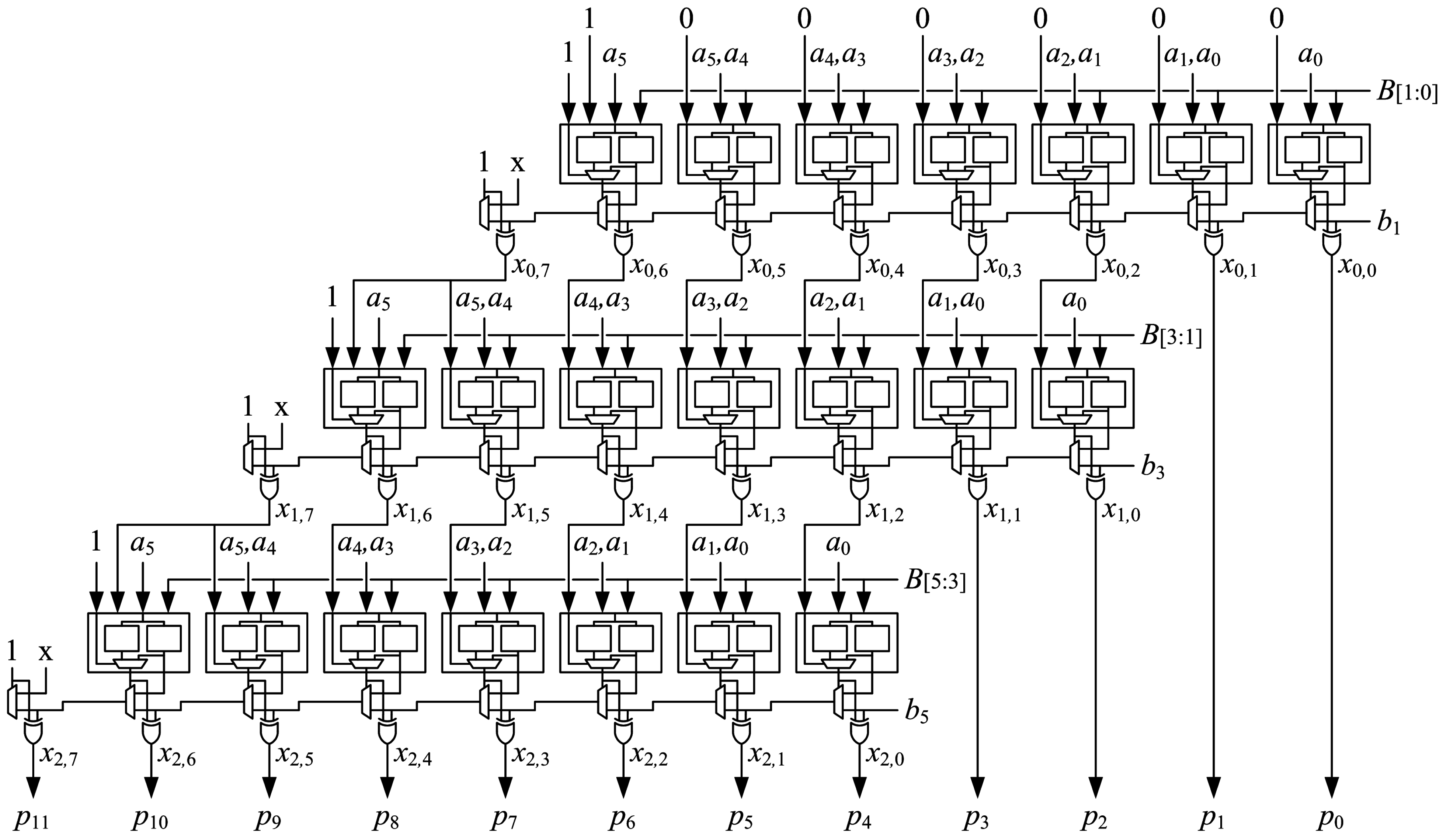
An array of optimized generate-add units is used to implement an multiplier. Optimized generate-add units are connected in an array structure as shown in Figure 11. Each generate-add unit requires LUT6s, so the number of LUT6s required to implement an array multiplier is:
The multiplier can be pipelined to reduce cycle time and increase throughput for applications that can tolerate increased latency. Figure 12 shows the connections for optimized generate-add units in a pipelined array multiplier with stages. The multiplier can be pipelined by placing a register after every two generate-add units to increase the maximum clock frequency with a modest increase in latency. All m bits of operand A and bits output from the second generate-add unit are registered at the end of the first stage. The three LSBs of operand B are not needed after the first stage, so only bits are registered. The two LSBs from the output of the first generate-add unit are also registered for a total of bits registered at the end of the first stage. In each subsequent stage, four fewer bits of B are registered while four additional LSBs from generate-add units are registered, so flip-flops are used to implement pipeline registers in each stage. There are pipeline registers, and flip-flops are needed to register the output, so the number of flip-flops required for an -stage pipelined array multiplier is:
Each of the LUT6s used to implement the array multiplier has two flip-flops, so there are flip-flops available within the footprint of the multiplier. If , there are enough flip-flops to implement an -stage pipeline with a significant number left over for other uses. This does not imply that all flip-flops used to implement the pipeline must be placed within the footprint of the multiplier. It does imply that a large number of multipliers can be densely placed on the FPGA fabric, and there will be enough flip-flops available within the logic of the multipliers for pipelining. Other designs that use the bypass input only have one flip-flop available per LUT6 and would not have enough flip-flops available for deep pipelining. If the product is truncated or rounded, the LSBs of the generate-add units do not need to be registered, and additional flip-flops are available for other uses.
The proposed array multipliers can also be pipelined with stages to further increase the maximum clock frequency. This is accomplished by placing pipeline registers after every generate-add unit. As with the -stage pipeline, this requires bits to be registered in each stage plus bits for the output register, so the number of flip-flops required for an -stage pipelined array multiplier is:
There are not enough flip-flops available within the footprint of the multiplier to implement an -stage pipeline. Unused flip-flops in nearby logic can be used to make up the difference if available. The number of required flip-flops can be reduced by using shift-register LUTs (SRLs). A single SRL can be used to replace a number of flip-flops connected as a shift register, such as the least-significant bits of the product that are shifted through each stage. The two flip-flops associated with the SRL are available for use, so using SRLs increases the number of flip-flops available in the multiplier footprint while reducing the number that is required. When SRLs are used to replace chains of three or more flip-flops, the Vivado synthesis default, there are more than enough flip-flops within the multiplier footprint to implement the -stage pipeline. As noted earlier, this does not imply that pipeline flip-flops must be placed with the footprint. Routing into or out of an SRL may be longer than the longest route between two flip-flops in a chain that it replaces, so it may be on the critical path and increase the delay of the multiplier.
The proposed array structure is easy to layout. LUT6s are placed in the fabric much like a mirror image of how they are shown in the schematic of Figure 11, which simplifies routing, as well. Deeper pipelining, i.e., using instead of stages, reduces delay significantly.
5.5. Row 0 Generate-Add Estimation Unit
The generate-add unit in the first row, , does not have an input value to add. The unit only needs to generate and add and to produce , the input to the next generate-add unit. Figure 13 shows the arithmetic for the Row 0 generate-add unit. If a maximum absolute error of one unit in the last place (ulp) can be tolerated, the generate-add unit in the first row can be replaced with an estimation unit that uses only LUT6s instead of . Figure 14 shows the Row 0 generate-add estimation unit, which produces an estimate, , instead of .
For any adjacent pair of bits in , each bit is a function of four variables:
Together, and are a function of five variables,
The two bits can be computed using two LUT5s in the same LUT6, generating at O6 and at O5. This allows to be generated using only LUT6s instead of the LUT6s required for a generate-add unit, but does not allow the fast carry chain to be used. Table 8 gives the truth table for a LUT6 that generates adjacent partial products and in the top row, Row 0.
The least-significant LUT6 can generate and , but cannot properly add because there cannot be a carry-out to the next LUT6. One option is to discard and simply output and . Another option is to generate and , add and output and if there is no carry out or and if there is a carry out. Another option is to output a function of , and that has a desired statistical result, such as an average error of zero.
The LUT5s that output for generate . The sum of and the two constant “1”s is . The LUT5s that output and generate and . As described in Section 5.3, the generate-add unit in the second row uses for and complements it internally, so does not need to be generated. The only error introduced into is the error from the least-significant LUT6, so the maximum absolute error is easily constrained to 1 ulp. Although not shown in Figure 14, could be generated using a single LUT5 and used for , and .
6. Results
The proposed multipliers are compared to Xilinx LogiCORE IP v12.0 multipliers [37] for signed -bit units. Results for 6-, 8-, 10-, 12-, 14-, 16-, 20-, 24-, 32- and 64-bit operands are given for single-cycle and pipelined units. Results from other work on GPC-based tree multipliers are compared, and the differences are discussed.
6.1. Methodology
Version 2014.4 of the Xilinx Vivado Design Suite was used. Designs were synthesized with the strategy set to “Vivado Synthesis Defaults” and implemented with the strategy set to “Performance_Retiming”. The -shreg_min_size parameter was set to the default value of three to synthesize pipelined versions of the proposed multipliers using SRLs and set to 99 to synthesize versions using flip-flops only. Designs were synthesized for the Virtex-7 XC7VX330T-FFG1157 (-3 speed grade) device with a timing constraint of 1 ns on the inner clock. All results are post place-and-route.
LogiCORE IP multipliers were created using the IP Catalog in Vivado. Area-optimized and delay-optimized units were synthesized for each operand size. Structural models of the proposed multipliers were implemented in Verilog. Single-cycle versions for each multiplier were created. Pipelined versions were created for LogiCORE multipliers using the optimal number of stages specified in the IP customization dialog. Pipelined versions of the proposed designs were created using and stages. -stage versions were synthesized using flip-flops only (no SRLs). Flip-flop-only designs and designs using SRLs were synthesized for -stage versions. Input and output ports were double registered to reduce dependence on I/O placement [38]. CARRY4 primitives were placed manually using the RLOC constraint, which specifies the relative location of primitives in the FPGA fabric. Placement of LUTs was done by the tools with no constraints. Placement of flip-flops was also done by the tools, and they were not constrained to the footprint of the multiplier. A separate clock on the inner level was used to measure the delay through each multiplier.
6.2. Single-Cycle Multipliers
Table 9 and Table 10 show synthesis results for single-cycle multipliers. The total number of LUTs used and the delay in nanoseconds of each multiplier are reported. The LUT-delay product (LDP) is computed as the total number of LUTs multiplied by the delay. This is analogous to the area-delay product of a VLSI design and gives a metric for comparing overall design efficiency, with lower values indicating higher efficiency. The reciprocal of LDP gives a metric for comparing throughput.
The area optimization for LogiCORE IP multipliers is most effective when both operands are unsigned [38]. Signed area-optimized LogiCORE multipliers were found to use more LUTs and to have a higher LUT-delay product than delay-optimized units for each of the operand sizes tested, so delay-optimized multipliers are used as the baseline for comparison. The total number of LUTs, maximum delay and LUT-delay product for each design are normalized to the delay-optimized LogiCORE multiplier of the same size.
The proposed single-cycle designs use 47%–51% fewer LUTs than the baseline LogiCORE multipliers, which allows approximately twice as many to be implemented in the same logic fabric. They are slower than baseline multipliers, and the normalized delay generally increases as n increases. For , the decrease in LUTs is more significant than the increase in delay, so those units have a 12%–46% lower LUT-delay product than baseline multipliers.
6.3. Pipelined Multipliers
Table 11, Table 12, Table 13, Table 14 and Table 15 show synthesis results for pipelined multipliers. The number of pipeline stages and the number of flip-flops (FFs) are reported. The number of flip-flops includes pipeline registers and one output register, but does not include the input registers or the second set of registers used to reduce dependence on I/O placement. Values are normalized to Xilinx LogiCORE IP multipliers reported in Table 11.
Table 12 shows proposed multipliers using an -stage pipeline and no SRLs. These versions use 47%–52% fewer LUTs than the baseline LogiCORE multipliers, which allows 1.90–2.10-times as many to be implemented in the same logic fabric. These versions use fewer flip-flops than LogiCORE multipliers. The LUTs used to implement each proposed multiplier have more associated flip-flops available for use than are used in the design because the bypass inputs are not used. These versions are generally slower than LogiCORE multipliers.
Table 13 shows proposed multipliers using an -stage pipeline and no SRLs. These versions use 47%–52% fewer LUTs and are 0%–23% faster than the baseline LogiCORE multipliers. These versions use more flip-flops than LogiCORE multipliers, and more flip-flops than are available from the associated LUTs used in the designs. If extra flip-flops are available from nearby logic, these versions offer LUT-delay products that are 52%–61% lower than baseline LogiCORE multipliers.
Table 14 shows proposed multipliers using an -stage pipeline and SRLs to save flip-flops. These versions use 42%–49% fewer LUTs and are 1%–22% faster than the baseline LogiCORE multipliers. These versions use fewer flip-flops than LogiCORE multipliers, and enough flip-flops are available from the associated LUTs. They have a 46%–55% lower LUT-delay product than baseline multipliers, indicating a potential 1.86–2.21-times increase in throughput for a fixed number of LUTs.
Table 15 shows proposed multipliers using an -stage pipeline, SRLs and a Row 0 estimation unit instead of a generate-add unit. These versions use 45%–49% fewer LUTs and are 4%–19% faster than the baseline LogiCORE multipliers. These versions use fewer LUTs and flip-flops than versions that use a generate-add unit, but may have slightly longer delay. They have a 49%–57% lower LUT-delay product than baseline multipliers, indicating a potential 1.97–2.33-times increase in throughput for a given number of LUTs.
6.4. Layout
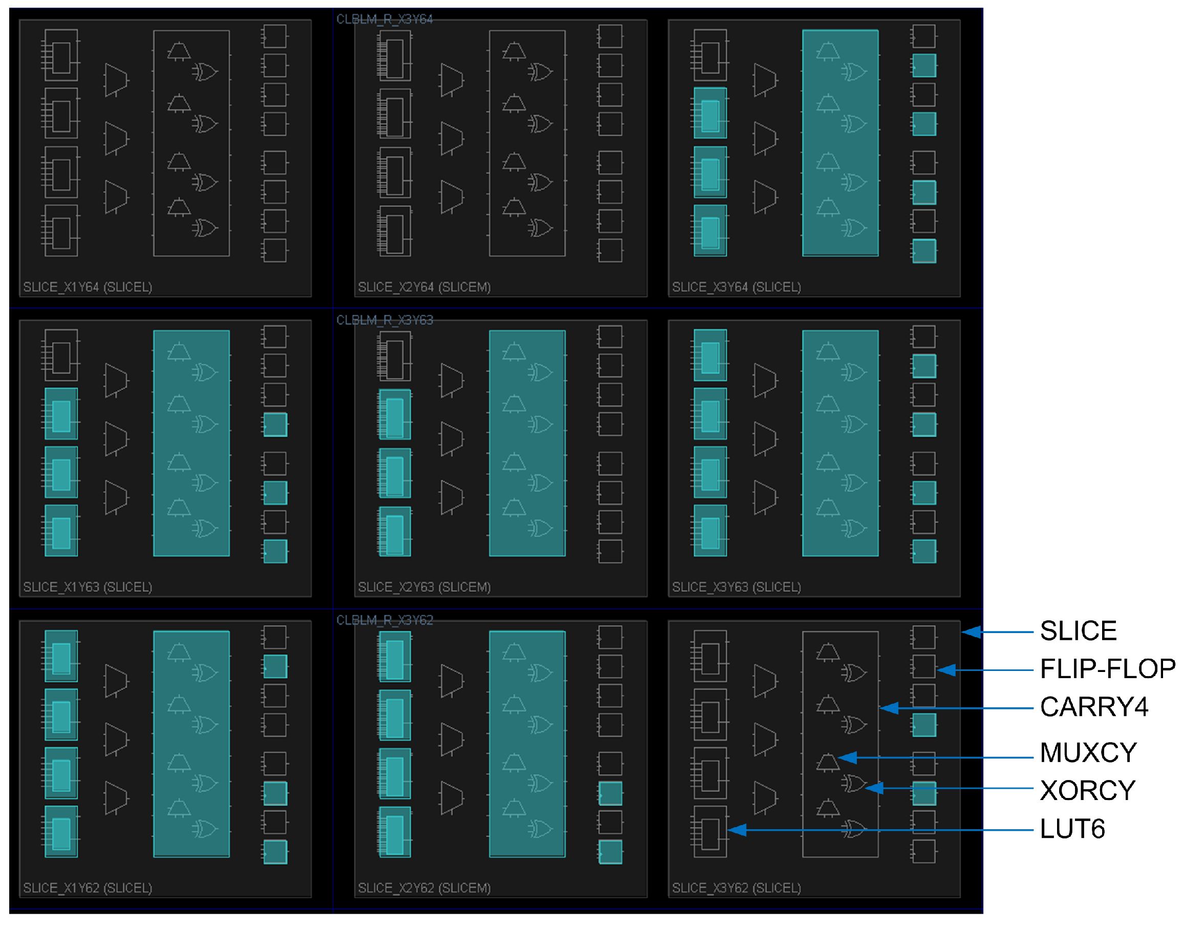
Figure 15 shows a screen capture of the implementation of a proposed single-cycle array multiplier (cf. the mirror image of Figure 11). Nine slices are shown in the screen capture, and primitives in the lower-right slice are annotated (cf. Figure 1). The four MUXCYs, four XORCYs and the fast carry chain for the slice are instantiated as a single Xilinx primitive called a CARRY4. Primitives that are used are indicated by a cyan background color. Note that in Figure 11, carries propagate from the right side of the figure to the left side, so that the most-significant bit of the product is on the left side and the least-significant bit is on the right side. In the screen capture, carries propagate from the bottom of the image to the top. The two slices in the left column of slices correspond to the generate-add unit that generates and outputs . The two slices in the middle column of slices correspond to the generate-add unit that generates and adds it to to output . The two slices in the right column of slices correspond to the generate-add unit that generates and adds it to to output . The flip-flops that are indicated as used are part of the registers used for the input and output ports to reduce dependence on I/O placement as noted in Section 6.1.
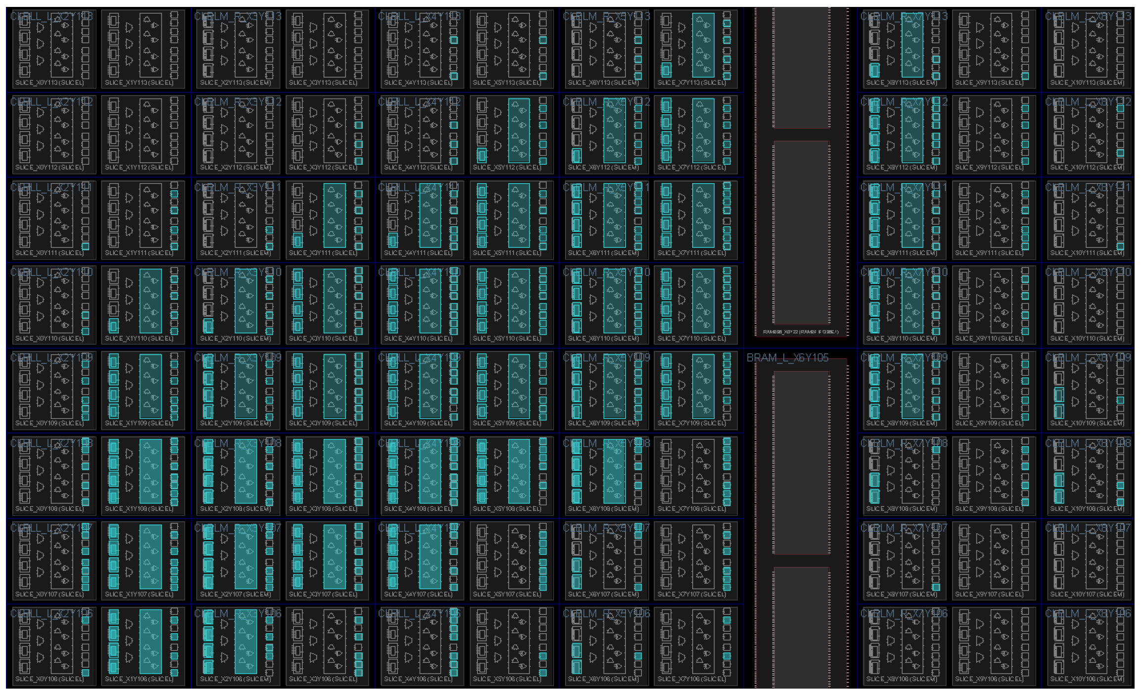
Figure 16 shows a screen capture of the implementation of a proposed pipelined multiplier, with an eight-stage pipeline using SRLs. The image on the left shows wiring from the I/O pads used for the bits of operand A to the first register for operand A. The flip-flops for the first register are generally located near the corresponding I/O pad. The wiring from the first register for operand A to the second register for operand A is not shown. Most of the flip-flops used for the second register for operand A are located near the multiplier logic at the top of the image. The image on the right shows the wiring from the second register for the output P to the I/O pads used for the bits of P. The flip-flops for the first output register for P are generally located close to the logic for the multiplier at the top of the image. This figure shows the importance of double-registering the input and output ports. If they were not double-registered, delays from long routing lines from I/O pads to the multiplier would give misleading results for the speed of a multiplier when used as part of a larger unit, such as a finite impulse response (FIR) filter that is not connected directly to I/O pads.
Figure 17 shows a screen capture of the implementation of the same eight-stage pipelined multiplier shown in Figure 16. This image shows a close-up view the multiplier logic shown at the top of the images in Figure 16. The eight generate-add units of the multiplier each occupy five slices in a column. The SRLs used in the multiplier are implemented using LUT6s in nearby slices. Most of the flip-flops in the slices are used for generate-add units, showing that the bypass inputs are indeed available and the bypass flip-flops can be used. The implementation was not constrained to use only those flip-flops. The tools implemented most of the pipeline registers using them, but left some of them unused and available while using some flip-flops in nearby slices.
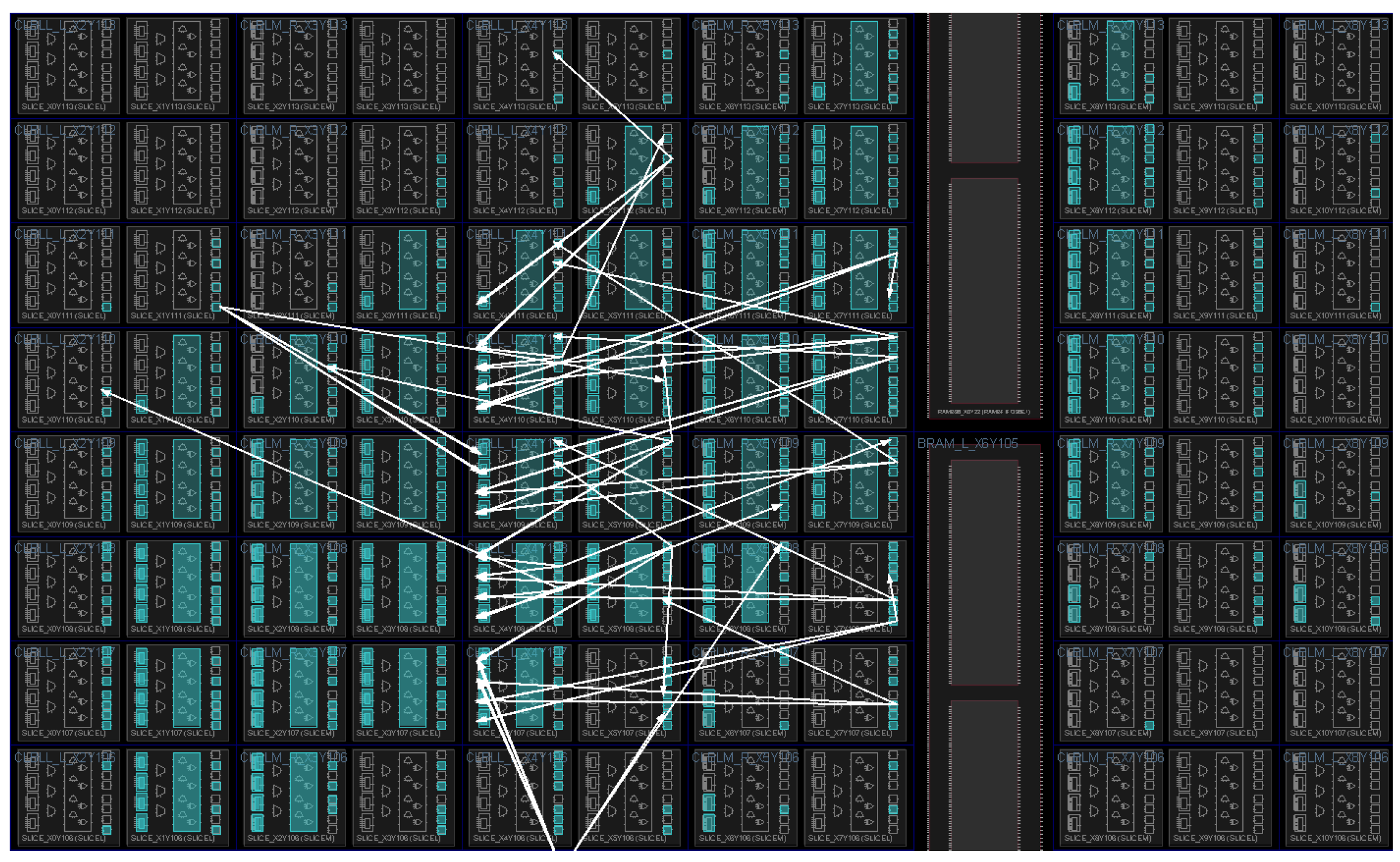
Figure 18 shows a screen capture of the same multiplier shown in Figure 17, plus the wiring from the pipeline register between the third and fourth pipeline stage to the inputs of the generate-add unit in the fourth stage. It can be seen that many of the flip-flops in the pipeline register are bypass flip-flops. However, some are not, and some are not in slices occupied by generate-add units. If many of the proposed -stage multipliers using SRLs were located next to each other, there would be enough flip-flops associated with the generate-add units and SRLs to implement all of the pipeline registers and an output register for each multiplier. However, without constraining the placement of those flip-flops, the tools would likely place some of the flip-flops for one multiplier in slices occupied by another multiplier. Further research is needed to determine if constraining flip-flops for a multiplier to the logic used to implement the same multiplier would yield any improvements in delay.
6.5. GPC-Based Tree Multipliers
Brunie et al. [18] present a data structure called a bit heap, which is similar to a BitMatrix object [4,39,40]. Bit heaps and BitMatrix objects treat a set of operands to be summed as a collection of individual weighted bits instead of a collection of operand vectors. The FloPoCo [41] arithmetic generator operates on bit heaps, applying embedded multipliers, GPCs and multipliers [42] to compute the sum. FloPoCo targets Altera and Xilinx FPGAs. Kumm and Zipf present two novel GPCs specific to Xilinx FPGAs that exploit the slice structure and are more efficient than previous work in terms of the ratio of the number of bits removed from the bit heap to the number of required LUTs. They then use ILP to select GPCs to reduce a bit heap to two rows and report improvements over the previous FloPoCo heuristic [19]. Mhaidat and Hamzah [20] present results for a Xilinx Spartan-6 FPGA, which uses a 6-input LUT architecture. They report that their multiplier uses 1133 LUTs, which is 2.15-times the number used by the proposed multipliers that do not use SRLs and 1.95-times the number used by the proposed -stage pipelined multipliers that use SRLs. They do not compare their results to LogiCORE IP, so normalized results for LUTs or delay are not available for comparison to proposed multipliers.
Two Altera ALMs can be used to implement a (6;3), a (1,5;3), a (2,3;3) or a (3,3;4) counter. (6;3) and (1,5;3) counters are favored because they eliminate three partial-product bits per counter, compared to (2,3;3) and (3,3;4) counters, which only eliminate two bits per counter. In Xilinx, three LUT6s would be required to implement a (6;3) or a (1,5;3) counter, because only five inputs can be shared between the LUT5s. A (2,3;3) counter could be implemented using two LUT6s, because there are only five inputs, so LUT5s can be used. A (3,3;4) counter would require four LUT6s. (6;3) and (1,5;3) counters can be used in Altera to eliminate 1.5 bits per ALM, but they would only eliminate one bit per LUT6 in Xilinx. The differences between Xilinx and Altera are too great to assume that results for GPC-based multipliers on Xilinx FPGAs would be comparable to results for Altera FPGAs presented in other work.
Parandeh-Afshar et al. compare LUT-based multipliers using GPCs to MegaWizard multipliers in Altera FPGAs in [7] and give a graph of the results. Numerical results are estimated from their graphs and tabulated in Table 16. Their radix-4 Booth multipliers have the best overall results. They are faster than MegaWizard multipliers at the expense of additional LUTs for most operand sizes. The normalized LUT-delay product ranges from 0.67 to 1.08. By contrast, the proposed multipliers are significantly smaller and have a much lower LUT-delay product than Xilinx LogiCORE IP multipliers when pipelined with -stages. This indicates that the proposed method has a larger improvement on Xilinx than [7] has on Altera.
7. Conclusions
This paper presents a novel two-operand adder that combines radix-4 partial-product generation and addition and shows how it can be used in FPGAs based on 6-input LUTs to implement two’s-complement array multipliers. Synthesis results are compared to Xilinx LogiCORE IP multipliers. The proposed array multipliers use approximately one-half of the LUTs needed by comparable LogiCORE IP multipliers, which allows approximately twice as many to be implemented in the same logic fabric. When deeply pipelined, the proposed multipliers are also faster than LogiCORE IP multipliers in most cases. SRLs can be used so that there are more flip-flops associated with the logic of the multiplier than required for pipelining, which allows a large number of deeply pipelined multipliers to be densely placed in the FPGA fabric. If a maximum absolute error of 1 ulp is tolerable, the number of required LUTs can be reduced further. The proposed multipliers are well suited for multiply-intensive applications, such as digital-signal processing, image processing and video processing, where they can be modified further using techniques, such as merged arithmetic and truncated-matrix arithmetic, to optimize the overall system.
Acknowledgments
The Xilinx Vivado Design Suite was obtained through the Xilinx University Program.
Conflicts of Interest
The author declares no conflict of interest.
Abbreviations
The following abbreviations are used in this manuscript:
| ALM | adaptive logic module |
| CLB | configurable logic block |
| CPA | carry-propagate adder |
| DSP | digital signal processing |
| FIR | finite impulse response |
| FPGA | field-programmable gate array |
| GPC | generalized parallel counter |
| ILP | integer linear programming |
| LAB | logic array block |
| LDP | LUT-delay product |
| LUT | lookup table |
| LUT5 | 5-input lookup table |
| LUT6 | 6-input lookup table |
| LSB | least-significant bit |
| MSB | most-significant bit |
| SRL | shift register LUT |
| ulp | unit in the last place |
References
- Swartzlander, E.E., Jr. Merged Arithmetic. IEEE Trans. Comput. 1980, C-29, 946–950. [Google Scholar] [CrossRef]
- Schulte, M.J.; Swartzlander, E.E., Jr. Truncated Multiplication with Correction Constant. In VLSI Signal Processing VI; IEEE Press: Eindhoven, The Netherlands, 1993; pp. 388–396. [Google Scholar]
- King, E.J.; Swartzlander, E.E., Jr. Data-Dependent Truncation Scheme for Parallel Multipliers. In Proceedings of the 31st Asilomar Conference on Signals, Systems, and Computers, Pacific Grove, CA, USA, 2–5 November 1997; Volume 2, pp. 1178–1182.
- Walters, E.G., III; Schulte, M.J. Design Tradeoffs Using Truncated Multipliers in FIR Filter Implementations. In Proceedings of the SPIE: Advanced Signal Processing Algorithms, Architectures, and Implementations XII, Seattle, WA, USA, 6 December 2002; Volume 4791, pp. 357–368.
- Walters, E.G., III; Arnold, M.G.; Schulte, M.J. Using Truncated Multipliers in DCT and IDCT Hardware Accelerators. In Proceedings of the SPIE: Advanced Signal Processing Algorithms, Architectures, and Implementations XIII, San Diego, CA, USA, 24 December 2003; Volume 5205, pp. 573–584.
- Walters, E.G., III. Linear and Quadratic Interpolators Using Truncated-Matrix Multipliers and Squarers. Computers 2015, 4, 293–321. [Google Scholar] [CrossRef]
- Parandeh-Afshar, H.; Ienne, P. Measuring and Reducing the Performance Gap between Embedded and Soft Multipliers on FPGAs. In Proceedings of the 21st International Conference on Field Programmable Logic and Applications, Chania, Greece, 5–7 September 2011; pp. 225–231.
- Parandeh-Afshar, H.; Brisk, P.; Ienne, P. Efficient Synthesis of Compressor Trees on FPGAs. In Proceedings of the Asia and South Pacific Design Automation Conference, Seoul, Korea, 21–24 January 2008; pp. 138–143.
- Parandeh-Afshar, H.; Brisk, P.; Ienne, P. Improving Synthesis of Compressor Trees on FPGAs via Integer Linear Programming. In Proceedings of the Design, Automation and Test in Europe, Munich, Germany, 10–14 March 2008; pp. 1256–1261.
- Parandeh-Afshar, H.; Brisk, P.; Ienne, P. Exploiting Fast Carry-Chains of FPGAs for Designing Compressor Trees. In Proceedings of the 2009 International Conference on Field Programmable Logic and Applications, Prague, Czech Republic, 31 August–2 September 2009; pp. 242–249.
- Parandeh-Afshar, H.; Verma, A.K.; Brisk, P.; Ienne, P. Improving FPGA Performance for Carry-Save Arithmetic. IEEE Trans. VLSI Syst. 2010, 18, 578–590. [Google Scholar] [CrossRef]
- Parandeh-Afshar, H.; Ienne, P. Highly Versatile DSP Blocks for Improved FPGA Arithmetic Performance. In Proceedings of the 2010 IEEE 18th Annual International Symposium on Field-Programmable Custom Computing Machines, Charlotte, NC, USA, 2–4 May 2010; pp. 229–236.
- Matsunaga, T.; Kimura, S.; Matsunaga, Y. Multi-Operand Adder Synthesis on FPGAs Using Generalized Parallel Counters. In Proceedings of the Asia and South Pacific Design Automation Conference, Taipei, Taiwan, 18–21 January 2010; pp. 337–342.
- Matsunaga, T.; Kimura, S.; Matsunaga, Y. Power and Delay Aware Synthesis of Multi-Operand Adders Targeting LUT-Based FPGAs. In Proceedings of the International Symposium on Low Power Electronics and Design, Fukuoka, Japan, 1–3 August 2011; pp. 217–222.
- Matsunaga, T.; Kimura, S.; Matsunaga, Y. An Exact Approach for GPC-Based Compressor Tree Synthesis. IEICE Trans. Fundam. Electron. Commun. Comput. Sci. 2013, E96-A, 2553–2560. [Google Scholar] [CrossRef]
- De Dinechin, F.; Pasca, B. Large Multipliers With Fewer DSP Blocks. In Proceedings of the 2009 International Conference on Field Programmable Logic and Applications, Prague, Czech Republic, 31 August–2 September 2009; pp. 250–255.
- Gao, S.; Al-Khalili, D.; Chabini, N. Implementation of Large Size Multipliers Using Ternary Adders and Higher Order Compressors. In Proceedings of the 21st International Conference on Microelectronics, Marrakech, Morocco, 19–22 December 2009; pp. 118–121.
- Brunie, N.; de Dinechin, F.; Istoan, M.; Sergent, G.; Illyes, K.; Popa, B. Arithmetic Core Generation Using Bit Heaps. In Proceedings of the 23rd International Conference on Field programmable Logic and Applications, Porto, Portugal, 2–4 September 2013; pp. 1–8.
- Kumm, M.; Zipf, P. Pipelined Compressor Tree Optimization Using Integer Linear Programming. In Proceedings of the 24th International Conference on Field Programmable Logic and Applications (FPL), München, Germany, 2–4 September 2014; pp. 1–8.
- Mhaidat, K.M.; Hamzah, A.Y. A New Efficient Reduction Scheme to Implement Tree Multipliers on FPGAs. In Proceedings of 2014 9th International Design and Test Symposium, Algiers, Algeria, 16–18 December 2014; pp. 180–184.
- Kumm, M.; Abbas, S.; Zipf, P. An Efficient Softcore Multiplier Architecture for Xilinx FPGAs. In Proceedings of the 22nd IEEE Symposium on Computer Arithmetic, Lyon, France, 22–24 June 2015; pp. 18–25.
- Walters, E.G., III. Partial-Product Generation and Addition for Multiplication in FPGAs With 6-Input LUTs. In Proceedings of the 48th Asilomar Conference on Signals, Systems, and Computers, Pacific Grove, CA, USA, 2–5 November 2014; pp. 1247–1251.
- Walters, E.G., III. Techniques and Devices for Performing Arithmetic. U.S. Patent Application 15/025,770, 25 August 2016. [Google Scholar]
- Walters, E.G., III. Techniques and Devices for Performing Arithmetic. U.S. Provisional Application 62/343,366, May 2016. [Google Scholar]
- Young, S.P.; Bauer, T.J. Programmable Integrated Circuit Providing Efficient Implementations of Arithmetic Functions. U.S. Patent 7,218,139, 15 May 2007. [Google Scholar]
- 7 Series FPGAs Configurable Logic Block User Guide; UG474 (v1.6); Xilinx: San Jose, CA, USA, August 2014.
- Stratix V Device Handbook, Volume 1: Device Interfaces and Integration; SV-5V1; Altera: San Jose, CA, USA, 2015.
- Stratix II Device Handbook, Volume 1; SII5V1-4.5; Altera: San Jose, CA, USA, 2011.
- Stratix 10 Advance Information Brief; AIB-01025; Altera: San Jose, CA, USA, 2015.
- MacSorley, O.L. High-speed Arithmetic in Binary Computers. Proc. IRE 1961, 49, 67–91. [Google Scholar] [CrossRef]
- Koren, I. Computer Arithmetic and Algorithms; Prentice Hall: Englewood Cliffs, NJ, USA, 1993. [Google Scholar]
- Ercegovac, M.D.; Lang, T. Digital Arithmetic; Morgan Kaufmann: San Francisco, CA, USA, 2004. [Google Scholar]
- Parhami, B. Computer Arithmetic: Algorithms and Hardware Design, 2nd ed.; Oxford University Press: New York, NY, USA, 2010. [Google Scholar]
- Wallace, C.S. A Suggestion for a Fast Multiplier. IEEE Trans. Electron. Comput. 1964, EC-13, 14–17. [Google Scholar] [CrossRef]
- Dadda, L. Some Schemes for Parallel Multipliers. Alta Frequenza 1965, 34, 349–356. [Google Scholar]
- Stenzel, W.J.; Kubitz, W.J.; Garcia, G.H. A Compact High-Speed Parallel Multiplication Scheme. IEEE Trans. Comput. 1977, C-26, 948–957. [Google Scholar] [CrossRef]
- LogiCORE IP Multiplier v12.0 Product Guide; PG108; Xilinx: San Jose, CA, USA, 2014.
- LogiCORE IP Multiplier v11.2 Product Specification; DS255; Xilinx: San Jose, CA, USA, 2011.
- Walters, E.G., III; Schulte, M.J.; Glossner, J. Automatic VHDL Generation of Parameterized FIR Filters. In Proceedings of the Second International Samos Workshop on Systems, Architectures, Modeling and Siulation, Samos, Greece, 22–25 July 2002; pp. 210–224.
- Walters, E.G., III. Using Truncated-Matrix Multipliers and Squarers in High-Performance DSP Systems. Ph.D. Thesis, Lehigh University, Bethlehem, PA, USA, January 2009. [Google Scholar]
- De Dinechin, F.; Pasca, B. Designing Custom Arithmetic Data Paths with FloPoCo. IEEE Des. Test Comput. 2011, 28, 18–27. [Google Scholar] [CrossRef]
- Kostarnov, I.; Whyte, A. Circuit Structure for Multiplying Numbers Using Look-Up Tables and Adders. U.S. Patent 8,352,532, 8 January 2013. [Google Scholar]
Figure 1.
Partial diagram of a Xilinx 7-Series CLB slice.

Figure 2.
Altera ALM configured as two 6-input LUTs.

Figure 3.
Altera ALM configured for arithmetic.
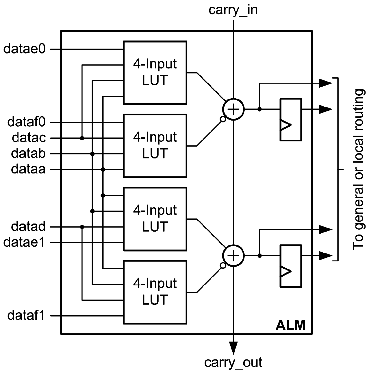
Figure 4.
Radix-4-modified Booth partial-product matrix, .

Figure 5.
Matrix reduction using (5,5;4) counters.

Figure 6.
Proposed two-operand adder; computing .
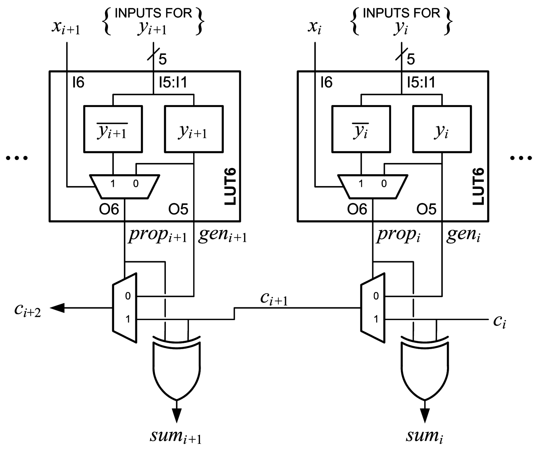
Figure 7.
Arithmetic for the partial-product generation and addition operation.

Figure 8.
Combined partial-product generation and addition unit.

Figure 9.
Arithmetic for the optimized generate-add operation.

Figure 10.
Optimized generate-add unit.

Figure 11.
Array structure of proposed multiplier, .

Figure 12.
Pipelined array multiplier with stages.
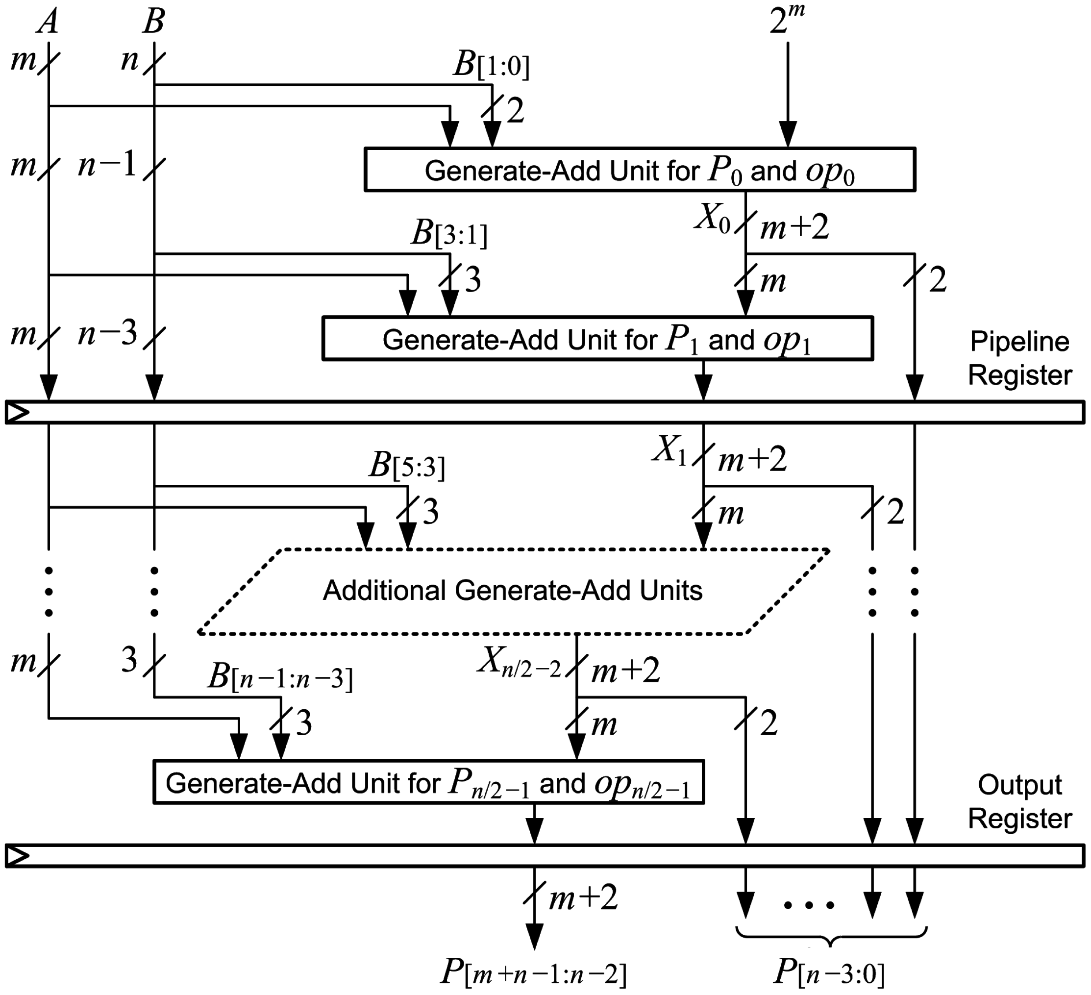
Figure 13.
Arithmetic for the Row 0 generate-add unit.
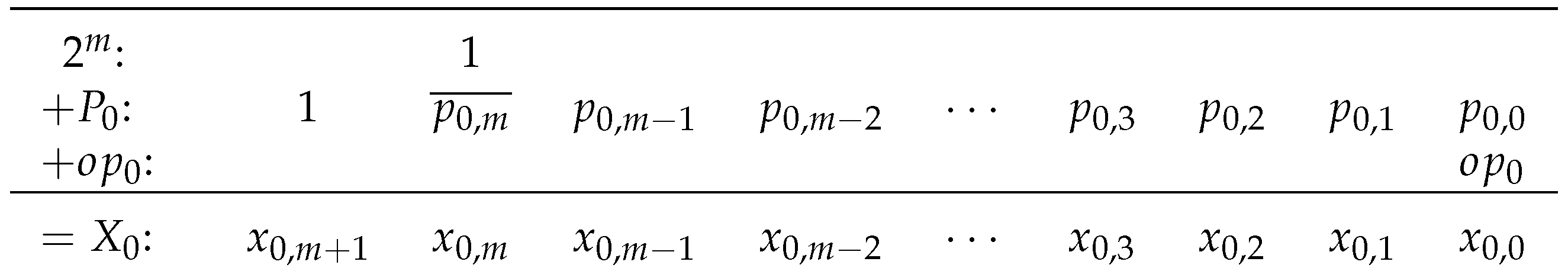
Figure 14.
Row 0 generate-add estimation unit.

Figure 15.
Implementation of the proposed single-cycle array multiplier.

Figure 16.
Implementation of the proposed pipelined multiplier (with an eight-stage pipeline using SRLs) showing wiring from the I/O pads for operand A on the left and wiring to the I/O pads for output P on the right.
Figure 16.
Implementation of the proposed pipelined multiplier (with an eight-stage pipeline using SRLs) showing wiring from the I/O pads for operand A on the left and wiring to the I/O pads for output P on the right.
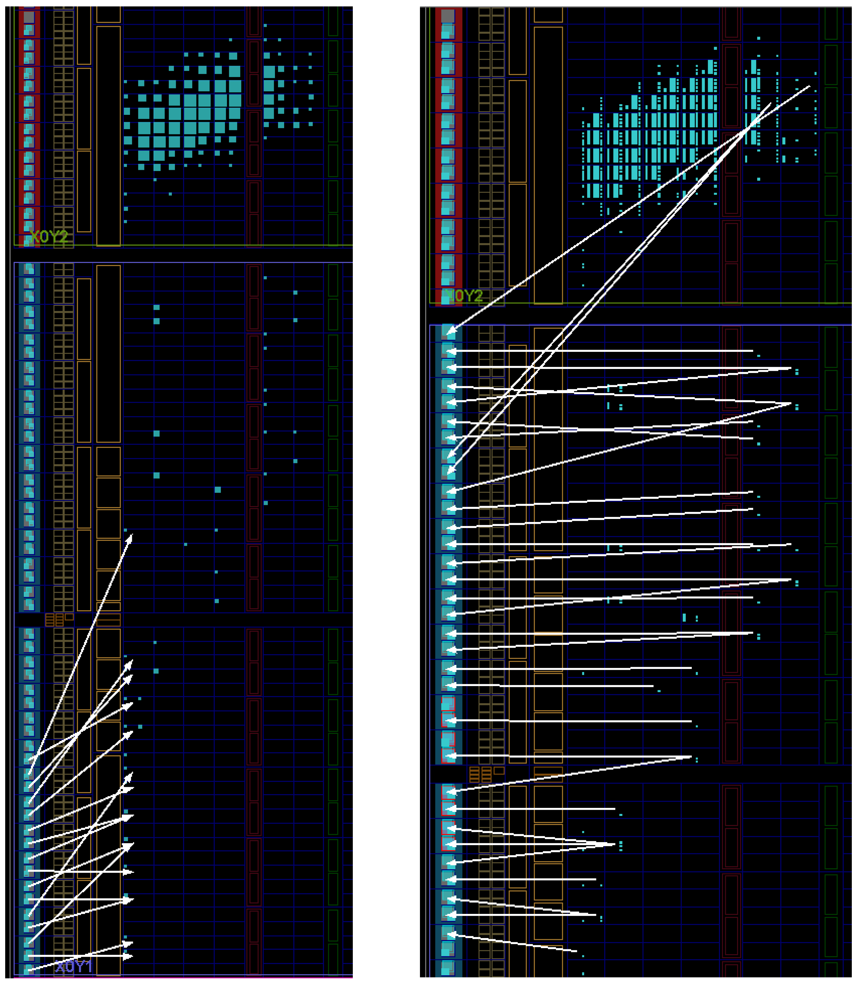
Figure 17.
Implementation of the proposed pipelined multiplier (with an eight-stage pipeline using SRLs) showing the usage of LUT6s, CARRY4s and flip-flops.
Figure 17.
Implementation of the proposed pipelined multiplier (with an eight-stage pipeline using SRLs) showing the usage of LUT6s, CARRY4s and flip-flops.

Figure 18.
Implementation of the proposed pipelined multiplier (with an eight-stage pipeline using SRLs) showing wiring from the third pipeline register to the fourth-stage generate-add unit.
Figure 18.
Implementation of the proposed pipelined multiplier (with an eight-stage pipeline using SRLs) showing wiring from the third pipeline register to the fourth-stage generate-add unit.


| Adder | Adder | MUXCY | ||||
|---|---|---|---|---|---|---|
| Inputs | Outputs | Inputs | ||||
| 0 | 0 | 0 | 0 | 0 | 0 | 0 |
| 0 | 0 | 1 | 0 | 1 | 0 | 0 |
| 0 | 1 | 0 | 0 | 1 | 1 | X |
| 0 | 1 | 1 | 1 | 0 | 1 | X |
| 1 | 0 | 0 | 0 | 1 | 1 | X |
| 1 | 0 | 1 | 1 | 0 | 1 | X |
| 1 | 1 | 0 | 1 | 0 | 0 | 1 |
| 1 | 1 | 1 | 1 | 1 | 0 | 1 |
| Comments | |||||
|---|---|---|---|---|---|
| 0 | 0 | 0 | 0 | 0 | string of “0”s |
| 0 | 0 | 1 | 1 | end of “1”s | |
| 0 | 1 | 0 | 1 | a single “1” | |
| 0 | 1 | 1 | 2 | end of “1”s | |
| 1 | 0 | 0 | beginning of “1”s | ||
| 1 | 0 | 1 | a single “0” | ||
| 1 | 1 | 0 | beginning of “1”s | ||
| 1 | 1 | 1 | 0 | 0 | string of “1”s |
| ⋯ | ||||||||
|---|---|---|---|---|---|---|---|---|
| 0 | 0 | 0 | ⋯ | 0 | 0 | 0 | 0 | |
| ⋯ | 0 | |||||||
| ⋯ | 0 | 0 | ||||||
| ⋯ | 1 | |||||||
| ⋯ | 1 | 1 |
| 0 | 0 | 0 | 0 | 0 |
| 0 | 0 | 1 | 1 | |
| 0 | 1 | 0 | 1 | |
| 0 | 1 | 1 | 2 | |
| 1 | 0 | 0 | ||
| 1 | 0 | 1 | ||
| 1 | 1 | 0 | ||
| 1 | 1 | 1 | 0 |
| ⋯ | ||||||||
|---|---|---|---|---|---|---|---|---|
| 0 | 0 | 0 | ⋯ | 0 | 0 | 0 | 0 | |
| ⋯ | 0 | |||||||
| ⋯ | 0 | 0 | ||||||
| 1 | 1 | 1 | ⋯ | 1 | 1 | 1 | 1 | |
| ⋯ | 1 | |||||||
| ⋯ | 1 | 1 |
| I5 | I4 | I3 | I2 | I1 | O6 | O5 | ||
|---|---|---|---|---|---|---|---|---|
| 0 | 0 | 0 | 0 | 0 | 0 | 0 | 1 | 0 |
| 0 | 0 | 0 | 0 | 1 | 0 | 0 | 1 | 0 |
| 0 | 0 | 0 | 1 | 0 | 0 | 0 | 1 | 0 |
| 0 | 0 | 0 | 1 | 1 | 0 | 0 | 1 | 0 |
| 0 | 0 | 1 | 0 | 0 | 1 | 0 | ||
| 0 | 0 | 1 | 0 | 1 | 1 | 0 | ||
| 0 | 0 | 1 | 1 | 0 | 0 | 1 | ||
| 0 | 0 | 1 | 1 | 1 | 0 | 1 | ||
| 0 | 1 | 0 | 0 | 0 | 1 | 0 | ||
| 0 | 1 | 0 | 0 | 1 | 1 | 0 | ||
| 0 | 1 | 0 | 1 | 0 | 0 | 1 | ||
| 0 | 1 | 0 | 1 | 1 | 0 | 1 | ||
| 0 | 1 | 1 | 0 | 0 | 1 | 0 | ||
| 0 | 1 | 1 | 0 | 1 | 0 | 1 | ||
| 0 | 1 | 1 | 1 | 0 | 1 | 0 | ||
| 0 | 1 | 1 | 1 | 1 | 0 | 1 | ||
| 1 | 0 | 0 | 0 | 0 | 0 | 1 | ||
| 1 | 0 | 0 | 0 | 1 | 1 | 0 | ||
| 1 | 0 | 0 | 1 | 0 | 0 | 1 | ||
| 1 | 0 | 0 | 1 | 1 | 1 | 0 | ||
| 1 | 0 | 1 | 0 | 0 | 0 | 1 | ||
| 1 | 0 | 1 | 0 | 1 | 0 | 1 | ||
| 1 | 0 | 1 | 1 | 0 | 1 | 0 | ||
| 1 | 0 | 1 | 1 | 1 | 1 | 0 | ||
| 1 | 1 | 0 | 0 | 0 | 0 | 1 | ||
| 1 | 1 | 0 | 0 | 1 | 0 | 1 | ||
| 1 | 1 | 0 | 1 | 0 | 1 | 0 | ||
| 1 | 1 | 0 | 1 | 1 | 1 | 0 | ||
| 1 | 1 | 1 | 0 | 0 | 1 | 0 | 1 | |
| 1 | 1 | 1 | 0 | 1 | 1 | 0 | 1 | |
| 1 | 1 | 1 | 1 | 0 | 1 | 0 | 1 | |
| 1 | 1 | 1 | 1 | 1 | 1 | 0 | 1 |
| f | |||||||||
|---|---|---|---|---|---|---|---|---|---|
| I5 | I4 | I3 | I2 | I1 | O6 | O5 | |||
| 0 | 0 | 0 | 0 | 0 | 1 | 0 | 0 | 0 | 1 |
| 0 | 0 | 0 | 0 | 1 | 0 | 0 | 0 | 1 | 1 |
| 0 | 0 | 0 | 1 | 0 | 1 | 0 | 0 | 0 | 1 |
| 0 | 0 | 0 | 1 | 1 | 0 | 0 | 0 | 1 | 1 |
| 0 | 0 | 1 | 0 | 0 | 1 | 0 | 1 | ||
| 0 | 0 | 1 | 0 | 1 | 0 | 1 | 1 | ||
| 0 | 0 | 1 | 1 | 0 | 1 | 1 | 0 | ||
| 0 | 0 | 1 | 1 | 1 | 0 | 0 | 0 | ||
| 0 | 1 | 0 | 0 | 0 | 1 | 0 | 1 | ||
| 0 | 1 | 0 | 0 | 1 | 0 | 1 | 1 | ||
| 0 | 1 | 0 | 1 | 0 | 1 | 1 | 0 | ||
| 0 | 1 | 0 | 1 | 1 | 0 | 0 | 0 | ||
| 0 | 1 | 1 | 0 | 0 | 1 | 0 | 1 | ||
| 0 | 1 | 1 | 0 | 1 | 0 | 1 | 1 | ||
| 0 | 1 | 1 | 1 | 0 | 1 | 1 | 0 | ||
| 0 | 1 | 1 | 1 | 1 | 0 | 0 | 0 | ||
| 1 | 0 | 0 | 0 | 0 | 1 | 1 | 0 | ||
| 1 | 0 | 0 | 0 | 1 | 0 | 0 | 0 | ||
| 1 | 0 | 0 | 1 | 0 | 1 | 0 | 1 | ||
| 1 | 0 | 0 | 1 | 1 | 0 | 1 | 1 | ||
| 1 | 0 | 1 | 0 | 0 | 1 | 1 | 0 | ||
| 1 | 0 | 1 | 0 | 1 | 0 | 0 | 0 | ||
| 1 | 0 | 1 | 1 | 0 | 1 | 0 | 1 | ||
| 1 | 0 | 1 | 1 | 1 | 0 | 1 | 1 | ||
| 1 | 1 | 0 | 0 | 0 | 1 | 1 | 0 | ||
| 1 | 1 | 0 | 0 | 1 | 0 | 0 | 0 | ||
| 1 | 1 | 0 | 1 | 0 | 1 | 0 | 1 | ||
| 1 | 1 | 0 | 1 | 1 | 0 | 1 | 1 | ||
| 1 | 1 | 1 | 0 | 0 | 1 | 1 | 1 | 0 | |
| 1 | 1 | 1 | 0 | 1 | 0 | 1 | 0 | 0 | |
| 1 | 1 | 1 | 1 | 0 | 1 | 1 | 1 | 0 | |
| 1 | 1 | 1 | 1 | 1 | 0 | 1 | 0 | 0 |
| I5 | I4 | I3 | I2 | I1 | O6 | O5 | |||
|---|---|---|---|---|---|---|---|---|---|
| 0 | 0 | 0 | 0 | 0 | 0 | 0 | 0 | 0 | 0 |
| 0 | 0 | 0 | 0 | 1 | 0 | 0 | 0 | 0 | 0 |
| 0 | 0 | 0 | 1 | 0 | 0 | 0 | 0 | 0 | 0 |
| 0 | 0 | 0 | 1 | 1 | 0 | 0 | 0 | 0 | 0 |
| 0 | 0 | 1 | 0 | 0 | 0 | 0 | 0 | 0 | 0 |
| 0 | 0 | 1 | 0 | 1 | 0 | 0 | 0 | 0 | 0 |
| 0 | 0 | 1 | 1 | 0 | 0 | 0 | 0 | 0 | 0 |
| 0 | 0 | 1 | 1 | 1 | 0 | 0 | 0 | 0 | 0 |
| 0 | 1 | 0 | 0 | 0 | 0 | 0 | |||
| 0 | 1 | 0 | 0 | 1 | 0 | 0 | |||
| 0 | 1 | 0 | 1 | 0 | 0 | 1 | |||
| 0 | 1 | 0 | 1 | 1 | 0 | 1 | |||
| 0 | 1 | 1 | 0 | 0 | 1 | 0 | |||
| 0 | 1 | 1 | 0 | 1 | 1 | 0 | |||
| 0 | 1 | 1 | 1 | 0 | 1 | 1 | |||
| 0 | 1 | 1 | 1 | 1 | 1 | 1 | |||
| 1 | 0 | 0 | 0 | 0 | 1 | 1 | |||
| 1 | 0 | 0 | 0 | 1 | 1 | 0 | |||
| 1 | 0 | 0 | 1 | 0 | 0 | 1 | |||
| 1 | 0 | 0 | 1 | 1 | 0 | 0 | |||
| 1 | 0 | 1 | 0 | 0 | 1 | 1 | |||
| 1 | 0 | 1 | 0 | 1 | 1 | 0 | |||
| 1 | 0 | 1 | 1 | 0 | 0 | 1 | |||
| 1 | 0 | 1 | 1 | 1 | 0 | 0 | |||
| 1 | 1 | 0 | 0 | 0 | 1 | 1 | |||
| 1 | 1 | 0 | 0 | 1 | 1 | 1 | |||
| 1 | 1 | 0 | 1 | 0 | 1 | 0 | |||
| 1 | 1 | 0 | 1 | 1 | 1 | 0 | |||
| 1 | 1 | 1 | 0 | 0 | 0 | 1 | |||
| 1 | 1 | 1 | 0 | 1 | 0 | 1 | |||
| 1 | 1 | 1 | 1 | 0 | 0 | 0 | |||
| 1 | 1 | 1 | 1 | 1 | 0 | 0 |
| Total | Delay | Normalized | |||||
|---|---|---|---|---|---|---|---|
| Type | n | LUTs | (ns) | LDP | LUTs | Delay | LDP |
| Xilinx | 6 | 40 | 2.581 | 103.2 | 1.000 | 1.000 | 1.000 |
| Xilinx | 8 | 72 | 2.662 | 191.7 | 1.000 | 1.000 | 1.000 |
| Xilinx | 10 | 110 | 3.533 | 388.6 | 1.000 | 1.000 | 1.000 |
| Xilinx | 12 | 158 | 3.666 | 579.2 | 1.000 | 1.000 | 1.000 |
| Xilinx | 14 | 214 | 3.728 | 797.8 | 1.000 | 1.000 | 1.000 |
| Xilinx | 16 | 280 | 3.937 | 1102.4 | 1.000 | 1.000 | 1.000 |
| Xilinx | 20 | 431 | 4.702 | 2026.6 | 1.000 | 1.000 | 1.000 |
| Xilinx | 24 | 617 | 4.885 | 3014.0 | 1.000 | 1.000 | 1.000 |
| Xilinx | 32 | 1089 | 5.514 | 6004.7 | 1.000 | 1.000 | 1.000 |
| Xilinx | 64 | 4261 | 7.259 | 30930.6 | 1.000 | 1.000 | 1.000 |
| Total | Delay | Normalized | |||||
|---|---|---|---|---|---|---|---|
| Type | n | LUTs | (ns) | LDP | LUTs | Delay | LDP |
| New | 6 | 21 | 2.649 | 55.6 | 0.525 | 1.026 | 0.539 |
| New | 8 | 36 | 3.594 | 129.4 | 0.500 | 1.350 | 0.675 |
| New | 10 | 55 | 4.250 | 233.8 | 0.500 | 1.203 | 0.601 |
| New | 12 | 78 | 5.248 | 409.3 | 0.494 | 1.432 | 0.707 |
| New | 14 | 105 | 5.820 | 611.1 | 0.491 | 1.561 | 0.766 |
| New | 16 | 136 | 6.875 | 935.0 | 0.486 | 1.746 | 0.848 |
| New | 20 | 210 | 8.509 | 1786.9 | 0.487 | 1.810 | 0.882 |
| New | 24 | 300 | 10.509 | 3152.7 | 0.486 | 2.151 | 1.046 |
| New | 32 | 528 | 13.956 | 7368.8 | 0.485 | 2.531 | 1.227 |
| New | 64 | 2080 | 26.323 | 54751.8 | 0.488 | 3.626 | 1.770 |
| Total | Delay | Normalized | |||||||
|---|---|---|---|---|---|---|---|---|---|
| Type | n | Stages | LUTs | (ns) | FFs | LUTs | Delay | FFs | LDP |
| Xilinx | 6 | 3 | 40 | 1.413 | 55 | 1.000 | 1.000 | 1.000 | 1.000 |
| Xilinx | 8 | 3 | 72 | 1.518 | 81 | 1.000 | 1.000 | 1.000 | 1.000 |
| Xilinx | 10 | 4 | 113 | 1.338 | 150 | 1.000 | 1.000 | 1.000 | 1.000 |
| Xilinx | 12 | 4 | 161 | 1.416 | 192 | 1.000 | 1.000 | 1.000 | 1.000 |
| Xilinx | 14 | 4 | 217 | 1.516 | 253 | 1.000 | 1.000 | 1.000 | 1.000 |
| Xilinx | 16 | 4 | 283 | 1.506 | 305 | 1.000 | 1.000 | 1.000 | 1.000 |
| Xilinx | 20 | 5 | 440 | 1.639 | 517 | 1.000 | 1.000 | 1.000 | 1.000 |
| Xilinx | 24 | 5 | 626 | 1.694 | 694 | 1.000 | 1.000 | 1.000 | 1.000 |
| Xilinx | 32 | 5 | 1099 | 1.836 | 1154 | 1.000 | 1.000 | 1.000 | 1.000 |
| Xilinx | 64 | 6 | 4288 | 2.358 | 4418 | 1.000 | 1.000 | 1.000 | 1.000 |
| Total | Delay | Normalized | |||||||
|---|---|---|---|---|---|---|---|---|---|
| Type | n | Stages | LUTs | (ns) | FFs | LUTs | Delay | FFs | LDP |
| New | 6 | 2 | 21 | 1.984 | 31 | 0.525 | 1.404 | 0.563 | 0.737 |
| New | 8 | 2 | 36 | 2.038 | 41 | 0.500 | 1.343 | 0.506 | 0.671 |
| New | 10 | 3 | 55 | 1.943 | 82 | 0.487 | 1.452 | 0.547 | 0.707 |
| New | 12 | 3 | 78 | 2.108 | 98 | 0.484 | 1.489 | 0.510 | 0.721 |
| New | 14 | 4 | 105 | 1.988 | 157 | 0.484 | 1.311 | 0.621 | 0.635 |
| New | 16 | 4 | 136 | 2.176 | 179 | 0.481 | 1.445 | 0.587 | 0.694 |
| New | 20 | 5 | 210 | 2.232 | 284 | 0.477 | 1.362 | 0.549 | 0.650 |
| New | 24 | 6 | 300 | 2.347 | 413 | 0.479 | 1.385 | 0.595 | 0.664 |
| New | 32 | 8 | 528 | 2.396 | 743 | 0.480 | 1.305 | 0.644 | 0.627 |
| New | 64 | 16 | 2080 | 2.855 | 3023 | 0.485 | 1.211 | 0.684 | 0.587 |
| Total | Delay | Normalized | |||||||
|---|---|---|---|---|---|---|---|---|---|
| Type | n | Stages | LUTs | (ns) | FFs | LUTs | Delay | FFs | LDP |
| New | 6 | 3 | 21 | 1.119 | 50 | 0.525 | 0.792 | 0.980 | 0.416 |
| New | 8 | 4 | 36 | 1.175 | 91 | 0.500 | 0.774 | 1.123 | 0.387 |
| New | 10 | 5 | 55 | 1.232 | 144 | 0.487 | 0.921 | 0.960 | 0.448 |
| New | 12 | 6 | 78 | 1.283 | 209 | 0.484 | 0.906 | 1.090 | 0.439 |
| New | 14 | 7 | 105 | 1.312 | 286 | 0.484 | 0.865 | 1.130 | 0.419 |
| New | 16 | 8 | 136 | 1.402 | 375 | 0.481 | 0.931 | 1.230 | 0.447 |
| New | 20 | 10 | 210 | 1.465 | 589 | 0.477 | 0.894 | 1.139 | 0.427 |
| New | 24 | 12 | 300 | 1.700 | 851 | 0.479 | 1.004 | 1.226 | 0.481 |
| New | 32 | 16 | 528 | 1.667 | 1519 | 0.480 | 0.908 | 1.316 | 0.436 |
| New | 64 | 32 | 2080 | 2.083 | 6111 | 0.485 | 0.883 | 1.383 | 0.429 |
| Total | Delay | Normalized | |||||||
|---|---|---|---|---|---|---|---|---|---|
| Type | n | Stages | LUTs | (ns) | FFs | LUTs | Delay | FFs | LDP |
| New | 6 | 3 | 23 | 1.193 | 46 | 0.575 | 0.844 | 0.836 | 0.485 |
| New | 8 | 4 | 42 | 1.176 | 77 | 0.583 | 0.775 | 0.951 | 0.452 |
| New | 10 | 5 | 65 | 1.251 | 116 | 0.575 | 0.935 | 0.773 | 0.538 |
| New | 12 | 6 | 92 | 1.318 | 163 | 0.571 | 0.931 | 0.849 | 0.532 |
| New | 14 | 7 | 123 | 1.292 | 218 | 0.567 | 0.852 | 0.862 | 0.483 |
| New | 16 | 8 | 158 | 1.349 | 281 | 0.558 | 0.896 | 0.921 | 0.500 |
| New | 20 | 10 | 240 | 1.441 | 431 | 0.545 | 0.879 | 0.834 | 0.480 |
| New | 24 | 12 | 338 | 1.674 | 613 | 0.540 | 0.988 | 0.883 | 0.534 |
| New | 32 | 16 | 582 | 1.824 | 1073 | 0.530 | 0.993 | 0.930 | 0.526 |
| New | 64 | 32 | 2198 | 2.050 | 4193 | 0.513 | 0.869 | 0.949 | 0.446 |
| Total | Delay | Normalized | |||||||
|---|---|---|---|---|---|---|---|---|---|
| Type | n | Stages | LUTs | (ns) | FFs | LUTs | Delay | FFs | LDP |
| New | 6 | 3 | 22 | 1.294 | 42 | 0.550 | 0.916 | 0.763 | 0.504 |
| New | 8 | 4 | 38 | 1.233 | 75 | 0.528 | 0.812 | 0.926 | 0.429 |
| New | 10 | 5 | 60 | 1.279 | 114 | 0.531 | 0.956 | 0.760 | 0.508 |
| New | 12 | 6 | 86 | 1.290 | 161 | 0.534 | 0.911 | 0.839 | 0.487 |
| New | 14 | 7 | 116 | 1.333 | 216 | 0.535 | 0.879 | 0.854 | 0.470 |
| New | 16 | 8 | 150 | 1.368 | 279 | 0.530 | 0.908 | 0.915 | 0.481 |
| New | 20 | 10 | 230 | 1.424 | 429 | 0.523 | 0.869 | 0.830 | 0.454 |
| New | 24 | 12 | 326 | 1.465 | 611 | 0.521 | 0.865 | 0.880 | 0.450 |
| New | 32 | 16 | 566 | 1.775 | 1071 | 0.515 | 0.967 | 0.928 | 0.498 |
| New | 64 | 32 | 2166 | 2.076 | 4191 | 0.505 | 0.880 | 0.949 | 0.445 |
Table 16.
Results for GPC-based multipliers on Altera [7].
| [7] Radix-4 Booth | [7] Baugh-Wooley | |||||
|---|---|---|---|---|---|---|
| Normalized to | Normalized to | |||||
| Altera MegaWizard | Altera MegaWizard | |||||
| n | LUTs | Delay | LDP | LUTs | Delay | LDP |
| 10 | 1.00 | 0.67 | 0.67 | 1.12 | 1.28 | 1.43 |
| 12 | 1.00 | 0.79 | 0.79 | 1.10 | 1.02 | 1.12 |
| 14 | 1.07 | 0.82 | 0.88 | 1.13 | 1.10 | 1.24 |
| 16 | 1.22 | 0.84 | 1.02 | 1.26 | 0.95 | 1.20 |
| 20 | 0.97 | 0.83 | 0.81 | 1.03 | 0.92 | 0.95 |
| 24 | 0.97 | 0.83 | 0.81 | 1.05 | 0.94 | 0.99 |
| 32 | 1.21 | 0.89 | 1.08 | 1.25 | 0.98 | 1.23 |
| 64 | 1.16 | 0.82 | 0.95 | 1.16 | 0.98 | 1.14 |
© 2016 by the author; licensee MDPI, Basel, Switzerland. This article is an open access article distributed under the terms and conditions of the Creative Commons Attribution (CC-BY) license (http://creativecommons.org/licenses/by/4.0/).
Share and Cite
MDPI and ACS Style
Walters, E.G. Array Multipliers for High Throughput in Xilinx FPGAs with 6-Input LUTs. Computers 2016, 5, 20. https://doi.org/10.3390/computers5040020
AMA Style
Walters EG. Array Multipliers for High Throughput in Xilinx FPGAs with 6-Input LUTs. Computers. 2016; 5(4):20. https://doi.org/10.3390/computers5040020
Chicago/Turabian StyleWalters, E. George. 2016. "Array Multipliers for High Throughput in Xilinx FPGAs with 6-Input LUTs" Computers 5, no. 4: 20. https://doi.org/10.3390/computers5040020
Note that from the first issue of 2016, this journal uses article numbers instead of page numbers. See further details here.