Article

Enhanced Photodegradation Activity of Hydrogen-Terminated Si Nanowires Arrays with Different-Oriented Crystal Phases

1
College of Physics and Cultivation Base for State Key Laboratory, Qingdao University, Qingdao 266071, China
2
National Institution Materials Society, 1-2-1 Sengen, Tsukuba, Ibaraki 3050047, Japan
3
School of Materials Science and Engineering Shandong, University of Science and Technology, Qingdao 266590, China
*
Authors to whom correspondence should be addressed.
These authors contributed equally to this work.
Catalysts 2017, 7(12), 371; https://doi.org/10.3390/catal7120371
Submission received: 14 October 2017 / Revised: 22 November 2017 / Accepted: 25 November 2017 / Published: 1 December 2017
(This article belongs to the Special Issue Nanostructured Materials for Applications in Heterogeneous Catalysis)

Abstract

:
Although Si nanowires (NWs) arrays are superior candidates for visible light photocatalysis, reports about the photodegradation activity of various crystal-orientated Si NWs are still insufficient. Here, light-doped hydrogen-terminated Si NWs arrays with different crystal orientations were prepared via a metal-assisted chemical etching method (MACE), which simply modulated the concentration of the oxidizer, H2O2. Their dye photodegradation activities were systematically and comprehensively investigated. When compared with Si NWs arrays with crystal orientations of (110) and (111), Si NWs arrays with (100) crystal orientation exhibit a superior photodegradation activity and stability due to the anisotropy of optical and physical properties. The n-type Si NWs arrays exhibit better photodegradation activity than the p-type Si NWs arrays of the same crystal orientation and similar length. The results provide a further understanding of the synthesis of Si NWs arrays with various orientations, and the relationships between photodegradation activity/stability and crystal orientations.

Graphical Abstract

1. Introduction

Over the past decades, Si nanowires (NWs) have attracted tremendous interests due to their excellent optical/electrical properties, high specific area, superior chemical/physical stability, and so on [1,2,3,4,5,6,7,8]. Owing to the special status as one-dimensional semiconductors, Si NWs have exhibited seductive application potentials in many fields, such as field effect transistors, solar cells, lithium-ion batteries, and photocatalysts [9,10,11,12,13,14,15,16,17,18,19,20]. In particular, due to the superior photocatalytic activity, Si NWs present a promising potency for future visible-light photocatalysts [19,21,22,23,24,25,26,27,28,29,30]. At present, two main methods, i.e., the vapor-liquid-solid (VLS) growth and the chemical etching (CE), are usually employed to prepare Si NWs photocatalysts. The Si NWs were firstly synthesized by the VLS method in 1964 [31], but it involves high fabrication costs, low productivity, complicated processing, and rigorous growth conditions. Hence, the VLS method is not suitable for the large-scale, low-cost, and easy-modulation fabrication. Moreover, the VLS growth method induces the deep electronic level in the band structure due to the noble metal catalyst tip on the top of NW, thereby degrading the minority-carrier life time and the diffusion length, while also depressing the photocatalytic activity [11,32,33,34]. It should be noted that the controllability of the growth direction of Si NWs is very challenging. Specifically, for the VLS method, crystal orientation of the fabricated vertically-aligned Si NWs is hard to control [35,36]. The crystal orientation of the Si NWs that are prepared by the VLS method was usually determined by the diameter of NWs. Si NWs with a small diameter prefer to grow along (110), whereas (111) is preferred by the Si NWs with larger diameter.
For practical applications, it is important to select an economical and efficient routine to fabricate Si NWs. Among the CE methods, the metal-assisted chemical etching (MACE) is considered as an alternative for fabricating large-scale, high-productivity, vertically-aligned Si NWs, in which metal catalysts (e.g., gold or sliver) in an etching solution of hydrofluoric acid (HF) and an oxidant (e.g., H2O2) assist the etching process [21,37]. In MACE, the diameter of the Si NWs can be determined by the morphology of the deposited metal catalysts, and the etching orientation depends on the crystal orientation of the selected Si substrate [4]. MACE is the preferred method to control the crystal orientations of Si NWs, because the etching direction generally depends on the orientation of the starting wafer. However, Si substrates always exhibit a preferred etching direction along (100) for all of the (100), (110), or (111) orientations [38], so a problem limited the preparations of differently oriented Si NWs is still remaining to be solved. Huang et al. found that the etching direction of Si (110) wafers mainly relied on the morphology of the deposited metal catalysts. They utilized an aluminum oxide (AAO) membrane as a mask to tune the morphology of metal catalysts, and the (110) orientated Si NWs were successfully synthesized. Although they demonstrated a novel method to control the etching direction, the utilization of the AAO mask can restrict the productivity of Si NWs and complicate the experimental procedure [39].
The crystal orientation of the porous Si wafers or Si NWs, especially those with small diameters, is one of the most critical factors and could profoundly affect the physical or chemical properties, such as photodegradation activity [39]. Xu et al. investigated the photodegradation activity of an etched porous Si wafer with p (100) and p (111) crystal orientations, and demonstrated that p (100) porous Si wafers displayed more ambitious photodegradation activity and stability than that of p (111) porous Si wafer [40]. However, these investigations on the various Si crystal orientation nanostructures were not very comprehensive and systematic. Moreover, especially regarding Si NWs, the reports are nonexistent.
The Si NWs are composited of a crystalline Si core with an amorphous SiO2 shell with thickness of 3–5 nm [1]. This SiO2 insulation layer could hinder the transport of electrons or holes, and influence the photodegradation activity of Si NWs. As far as we know, Si-H bonds play a more critical role in this aspect of the dye photodegradation of Si NWs, which can accelerate the separation of holes and electrons. In our previous report, Si–O bonds were easily converted into Si–H bonds through a simple HF treatment, and the obviously enhanced photodegradation activity of HF-treated p (100) Si NWs was observed [21]. Simultaneously, Shao et al. investigated the performance of hydrogen-terminated Si NWs (H–Si NWs) and noble metal-decorated (Pt, Pd, Au, Rh, Ag) Si NWs under visible light irradiation, and found that the H–Si NWs exhibited a superior photodegradation activity in comparison with the metal-decorated Si NWs [22].
In this work, we obtained p-type and n-type Si NWs by a rapid, facile MACE method. In order to limit the effect of mesopores, light-doped p-type and n-type Si wafers were selected as the starting material. The photodegradation activity and stability of Si NWs with various crystal orientations were comprehensively and systematically investigated. When compared with (110) and (111)-oriented Si NWs arrays, Si NWs arrays with crystal orientation (100) exhibited superior photodegradation activity and stability. Additionally, for the same crystal orientation, n-type Si NWs arrays exhibited more photodegradation activity than p-type Si NWs arrays. These results help to further the understanding and investigations of Si NWs for the future photocatalytic applications.

2. Results and Discussion

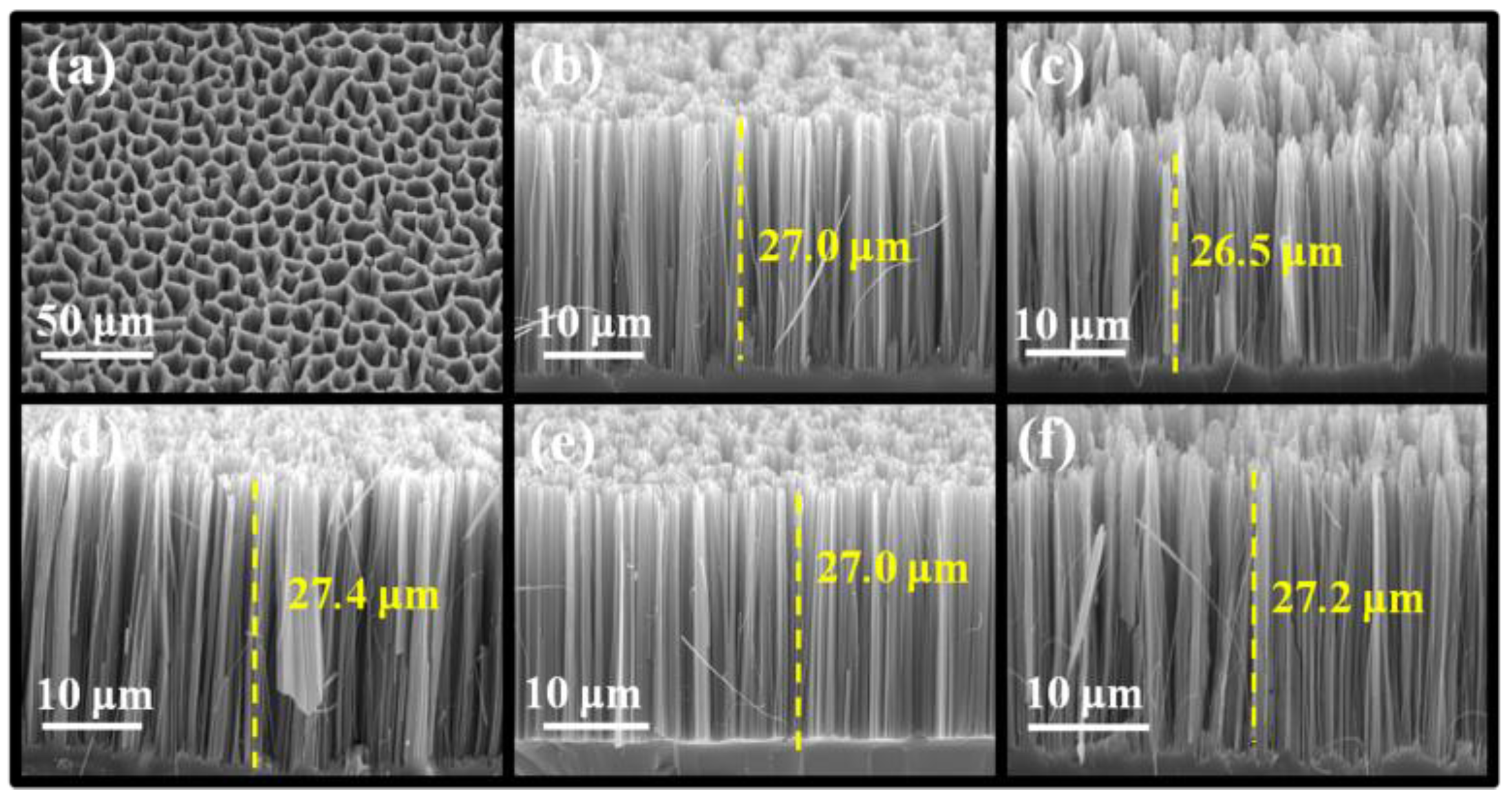
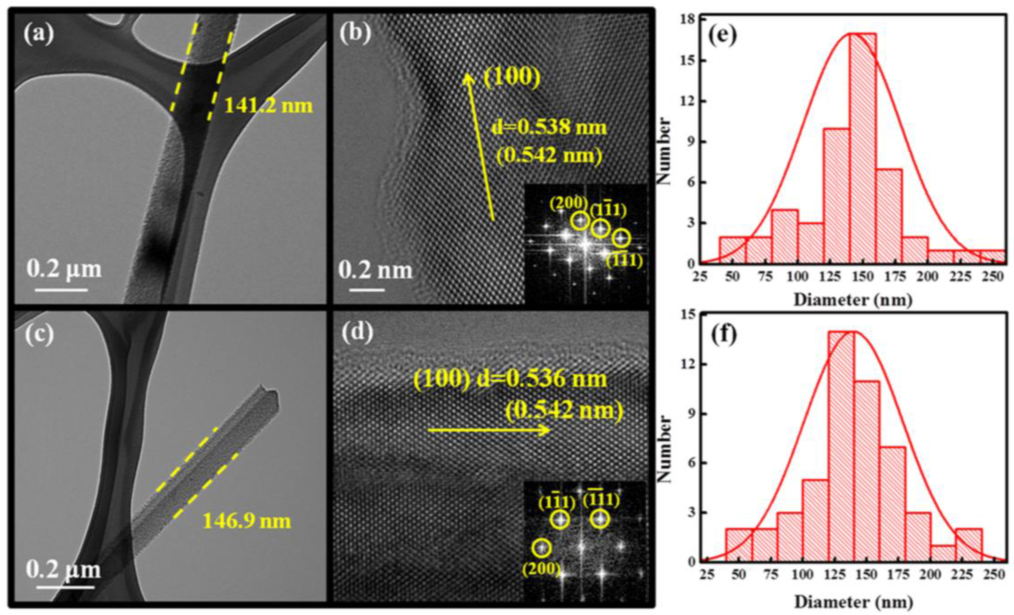
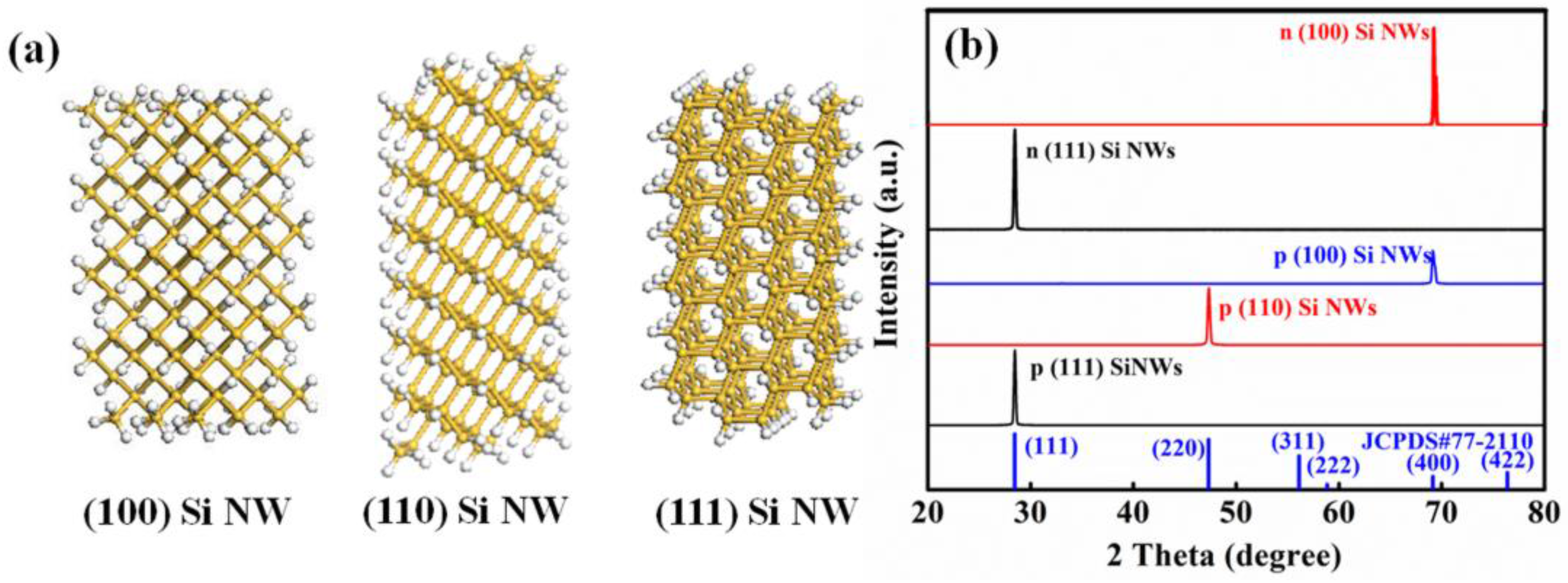
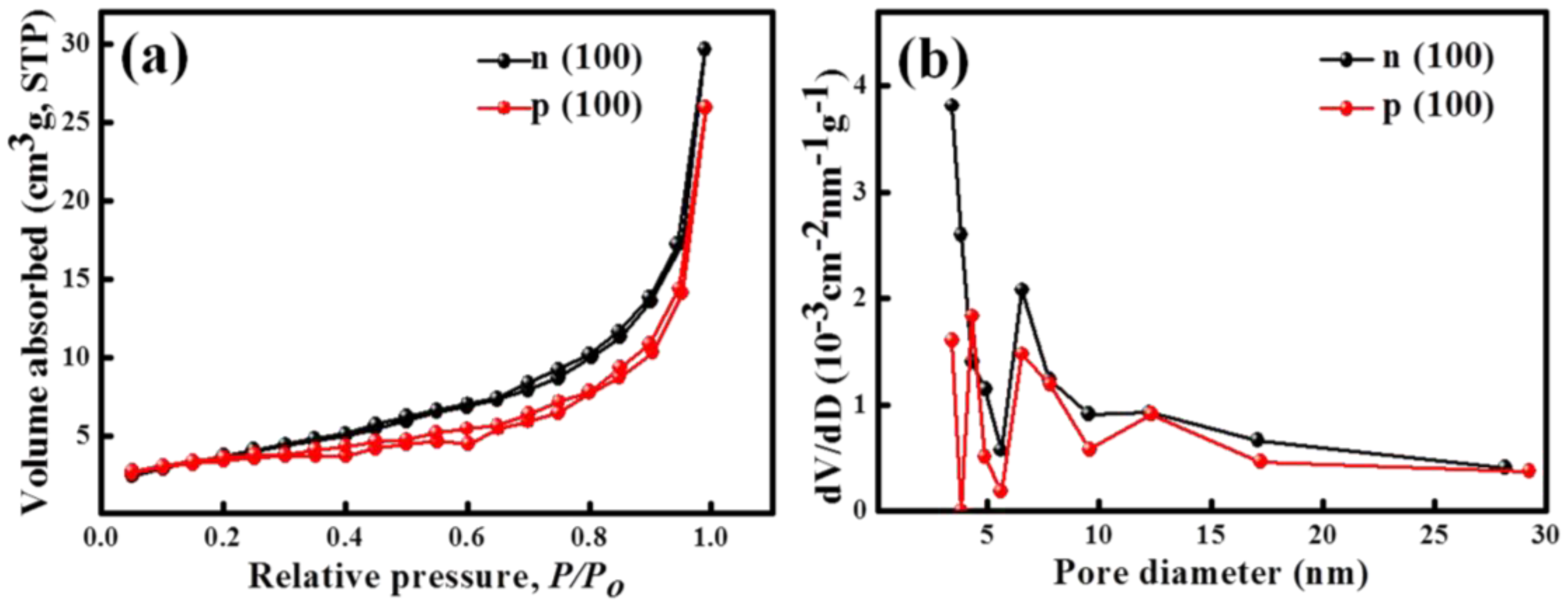
2.1. Characterization of Si NWs

To exclude the influence of different lengths, the Si NWs with various crystal orientations must possess similar lengths. Additionally, light-doped Si wafers were selected as the starting substrate to avoid the effect of mesopores. Etched, heavy-doped Si NWs produce a considerable amount of mesopores, which would be uncontrollable in the experimental process [21]. To study the morphology of Si NWs, Scanning Electron Microscope (SEM) images were performed at the same sample stage with a fixed angle. Figure 1a shows the top-view SEM image of as-synthesized p (100) Si NWs arrays, demonstrating that the Si NWs are uniformly distributed on the surface of the Si substrate and form congregated bundles and mesopores, which may be attributed to electrostatic attraction. The sectional SEM images of the samples with different crystal orientations are shown in Figure 1b–f, which correspond to the crystal orientations of p (100), p (110), p (111), n (111), and n (100), respectively, demonstrating the dense, distinguishable, uniform, straight, and vertical coverage of Si NWs on the Si substrate surface. Comparing Figure 1b–d, we can observe the differences in morphology of p (100), p (110), and p (111) Si NWs arrays. The Si NWs arrays with p (100) orientation display a more uniform length than the p (110) and p (111) Si NWs. The average length of NWs is controlled to be 27.0 ± 0.25, 26.5 ± 0.82, and 27.4 ± 0.65 μm for p (100), p (110), and p (111) Si NWs arrays, respectively. This can be obtained from a statistical error map of 50 NWs, as shown in Figure S1. It indicates that the Si NWs with different orientations possess similar lengths and the differences are negligible. Except for p (100), p (110), and p (111) Si NWs, n (100), and n (111) Si NWs arrays are also fabricated with the length of 27.0 ± 0.2, and 27.2 ± 0.95 μm, as provided in Figure 1e,f, which exhibits the same differences as the p-type Si NWs. Additionally, according to the across-sectional SEM images, the density of the five kinds of Si NWs (Figure 1b–f) generally keep the same order of magnitude, 1010/cm2. These differences can be ascribed to the complexity variation of the etching process, and the fact that the Si substrate with (100) orientation is more easily etched than the (110) and (111). This is because that the Si atom on the surface of the (100) Si NW has two back bonds, whereas the surface of (110) and (111) NWs possess three back bonds, as demonstrated in Figure 2a. This allows for the (100) Si NW to be etched more easily than the (110) and (111) Si NW. The Si NWs arrays with (110) and (111) orientations need to be etched using higher concentration of H2O2, which is detailed in the experimental section. When comparing the p (100) and n (100) Si NWs arrays, we can see that the differences in morphology, length, and density are negligible, indicating the indiscrimination between n-type and p-type Si NWs with the same orientation. The same results can be also obtained from the comparison between p (111) and n (111) Si NWs arrays. In general, the morphology, length, and density of Si NWs were kept at almost identical conditions, and the crystal orientation or conduction type were the only variable factor in order to enable the feasibility and accuracy of the experiment.
For a further understanding of the crystal structures of Si NW with various orientations, their H-terminated, automatic constructions for intrinsic Si NWs are shown in Figure 2a, in which the atoms density is apparent, leading to the differences in etching rate. Meanwhile, in order to ensure the accuracy of etched Si NWs crystal orientations, XRD spectra of Si NWs with p (100), p (110), p (111), n (100), and n (111) orientations were conducted, as shown in Figure 2b. Each kind of Si NWs exhibits a single, sharp peak, and all of them agree with the JCPDS#77-2110. No impurities and the secondary phases can be observed in the spectra, demonstrating the high purity of the products. The results indicate the accuracy of the etched Si NWs crystal orientation. Next, TEM was performed to further investigate the crystal structure and morphology of n- and p-type Si NWs, with (100) orientation. Figure 3a,c shows the TEM images of the single p (100) and n (100) Si NWs with a diameter of 141.2 nm and 146.9 nm, illustrating a relatively smooth and uniform surface. The corresponding High Resolution Transmission Electron Microscopy (HRTEM) together with the fast Fourier transform (FFT) are provided in Figure 3b,d, respectively. The interplanar spacing is measured to be 0.538 nm and 0.536 nm, which is slightly different from the ideal value of 0.542 nm because of the light-doped element. Additionally, FFT patterns transferred from HRTEM images by DigitalMicrograph software (DM3.9, Gatan, Pleasanton, CA, USA) are in consistence with the standard XRD and crystal lattice images, indicating that Si NWs have the same growth direction of (100), which is also the surface orientation of their starting wafers. To comprehensively evaluate the diameter of p (100) and n (100) Si NWs, the histograms of 50 Si NWs for the p (100) and n (100) Si NWs, respectively, demonstrate a standard normal distribution, as shown in Figure 3e,f. In the histograms, the diameter of n (100) or p (100) Si NWs always falls in the range of 125~175 nm. When comparing the measured lengths, the length/width can roughly reach 200~300, indicating a high specific area. This high specific area can absorb the most of incident solar energy and allow for a wider application of Si NWs in the visible-light photodegradation field. Additionally, from the TEM images, the morphology differences, including the uniformity and the diameter differences between p (100) and n (100) Si NWs, can be ignored.
To characterize the specific area of p (100) and n (100) oriented Si NWs, nitrogen absorption-desorption isotherms and the corresponding pore size distribution were performed. The isotherms of both n (100) and p (100) Si NWs arrays in Figure 4a show a type II-IV curve, indicating the typical characteristics of nonporous materials. The absorption isotherm of n (100) Si NWs arrays exhibits a sharp increase in the P/Po = 0.8–0.99 and a negligible hysteresis loop, which corresponds to the accumulation of Si NWs, demonstrating the nonporous characteristic of light-doped n (100) Si NWs. At the same time, non-porosity can be observed in the pore size distribution curves shown in Figure 4b, revealing that the mesoporosity as an interference factor can be eliminated. Even though mesoporosity is excluded, the multipoint Brunauer-Emmett-Teller (BET) analysis and Barett-Joyner-Halenda (BJH) of the absorption isotherm reveal a relatively large surface area of 13.88 m2/g and 11.52 m2/g, and an insignificant total pore volume of 0.045 cm3/g and 0.04 cm3/g for n (100) Si NWs and p (100) Si NWs, respectively. These results are consisted with our previous work [21] and show a large surface/volume ratio which have large advantages in the aspect of dye photodegradation applications.

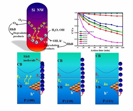
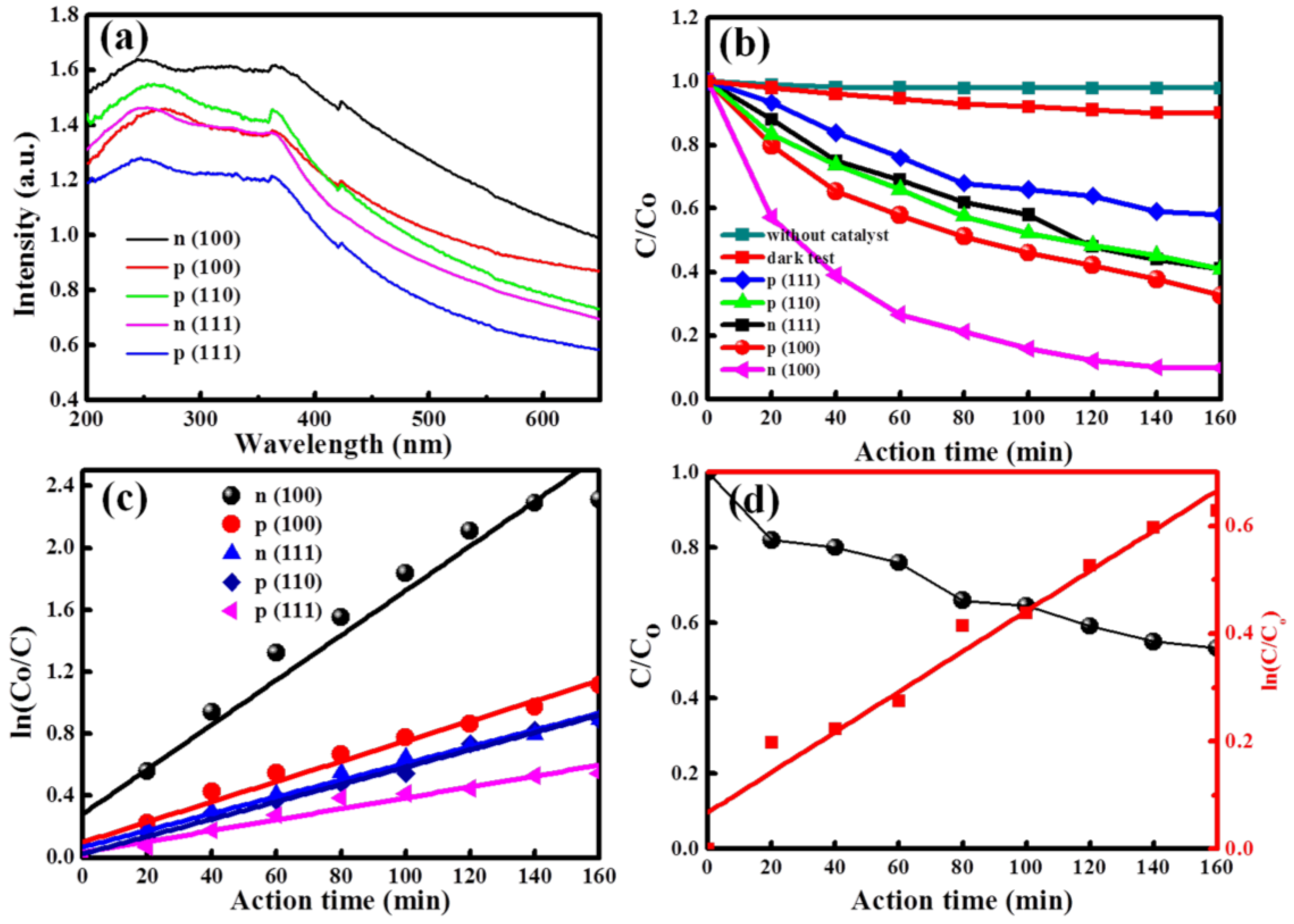
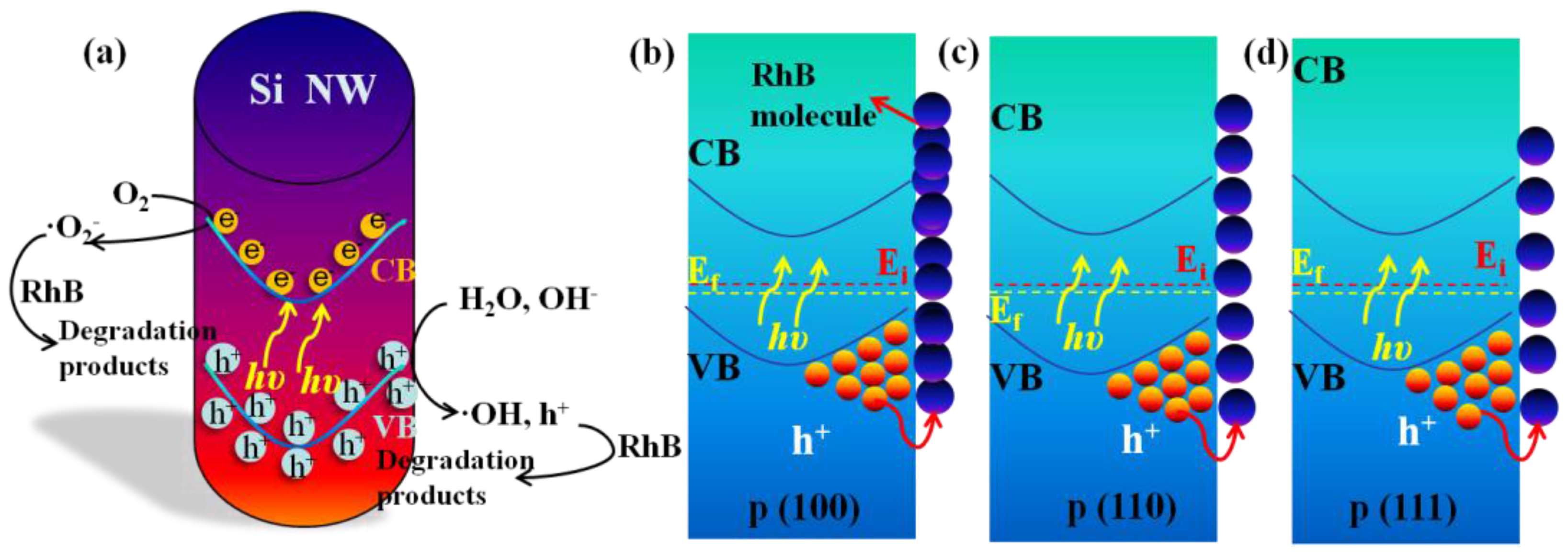
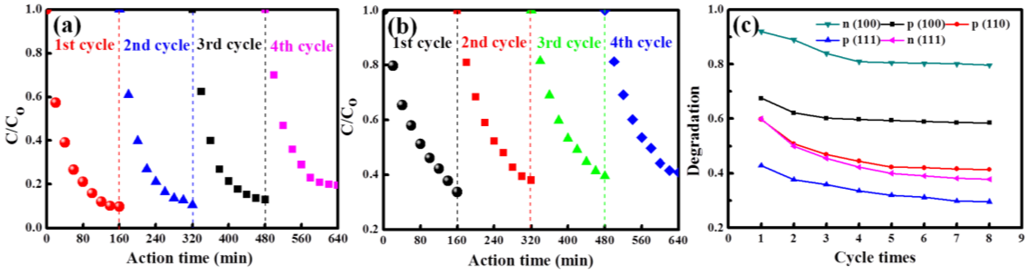
2.2. Photodegradation Activity of Si NWs with Various Crystal Orientations

To shed light on the photodegradation activity of Si NWs arrays with various orientations, rhodamine b (RhB), which is shown in Figure S3, was employed as an organic dye to verify and compare the Si NWs arrays photodegradation activity. Figure 5a shows the absorption spectra for p (100), p (110), p (111), n (100) and n (111) Si NWs arrays with nearly the same length and density on 1 cm × 1 cm substrates in an ambient atmosphere, exhibiting superior absorption under the visible light region, as expected [21]. From the absorption spectra, we can see clearly that Si NWs with the crystal orientation (100) exhibit more visible light absorption than Si NWs with crystal orientations (110) and (111). To ensure the feasibility and compare the photodegradation activity of the Si NWs with various crystal orientations, their photodegradation activity was evaluated using a 150 W Xenon lamp. The samples used in the RhB degradation were pre-treated using 5% HF for 1 min to convert the Si–O bonds into Si–H bonds. The experiments were all conducted in the ambient atmosphere and all of the samples were of the same length, density, and diameter. Figure 5b displays C/Co vs. action times curves, showing the decrease of the concentration of RhB, when compared with an initial RhB concentration of 5 × 10⁻⁶ mol/L. The RhB degradation was only 2% without the participation of the catalyst for the 160 min illumination period, indicating the importance of catalysts for RhB degradation. To evaluate the integral role of visible light, a test of the n (100) Si NWs in a black box was conducted and a RhB degradation of 9.8% was obtained, revealing that the optical excitation does play a key role in the RhB degradation. In contrast, the degradation ratio of RhB are 67.5%, 59.8%, 42.8%, 92%, and 60% for p (100), p (110), p (111), n (100), and n (111) Si NWs, respectively, after 160 min. The corresponding changes to the absorption peak are shown in Figure S2a–e, for p (100), p (110), p (111), n (100), and n (111) Si NWs. It is obvious that the bright red RhB solution is changed into a transparent, clear solution after degradation by n (100) Si NWs and under illumination of visible-light for 160 min (Figure S2f). According to the Langmuire-Hinshelwood (L-H) kinetics model, the photodegradation process can be described as a “pseudo-first-order kinetics equation”:
ln ( C o C ) = kt
where Co is the initial RhB concentration, C is the RhB concentration at the action time t, and k is the apparent rate constant. The corresponding linear fit graph of ln(Co/C) is shown in Figure 5c, and the obtained k values are 6.7 × 10⁻³, 5.7 × 10⁻³, 3.5 × 10⁻³, 1.5 × 10⁻², 5 × 10⁻³ s−1 for p (100), p (110), p (111), n (100), and n (111) Si NWs arrays, respectively, as shown in Table S1. This is consistent with the degradation ratio that is shown in Figure 5c. These results fully and comprehensively demonstrate that the Si NWs arrays with the orientation (100) exhibit superior photodegradation activity when compared with the (110) and (111) Si NWs arrays. Besides, n-type Si NWs usually display better photodegradation activity as compared with p-type Si NWs when the crystal orientations are identical. This can be mainly attributed to the high electron concentration in n-type Si [41]. In order to evaluate the feasibility and accuracy of the experiment, ten times repetition were made and the corresponding results was counted, as shown in Figure S4. In addition, it is worth noting that the Si–H bonds play a significant role in enhancing the photodegradation activity, because the hydrogen atom has a large Pauling electron negative value of 2.2. The terminated hydrogen atom with a charge of 0.09–0.13 au may also be employed as an electron sink to accelerate the separation of the electron and hole. So, for the purpose of evaluating the role of Si-H bonds, the n (100) Si NWs without HF pre-treatment was utilized to degrade polluted RhB. For the 160 min visible light illumination, the degradation ratio shown in Figure 5d was 46.3% together with the corresponding apparent rate k of 3.6 × 10⁻³ s−1, indicating decreased photocatalytic activity when compared with the H-terminated Si NWs. The dye photodegradation mechanism of H-terminated Si NW is shown in Figure 6a.
These distinctions on the degradation activity can be explained by the difference of the surface energy of the Si NWs with various orientations. In this case, more RhB molecules are absorbed on the surface of (100) Si NWs due to its larger surface free energy when compared with that of (110) and (111) oriented Si NWs, as shown in Figure 6b–d, leading to more RhB molecules being absorbed by the surface of the Si NWs [37,42,43].
Generally, the stability of photocatalysts is one of the most serious challenges hindering their practical application. Thus, the photodegradation cycle stability was measured and compared, as shown in Figure 7. The cycle measurements of n (100) Si NWs are presented in Figure 7a, in which the degradation ratio decreased from 92 to 80.6% after four cycles. For comparison with the stability of n (100) Si NWs arrays, the cycle measurements of p (100) Si NWs, as shown in Figure 7b, exhibit a decrease from 67.5 to 60% after four cycles. To further evaluate the stability of Si NWs with various crystal orientations, the degradation ratios of five kinds of Si NWs were obtained after eight cycles and statistics completed. Figure 7c shows the variation trend of the cycle measurements. After eight cycle measurements, the degradation ratio of p (100) Si NWs decreases from 67.5 to 58.7%, exhibiting a slightly decrease of photodegradation activity. Notably, no obvious degradation can be observed after the third measurement in the RhB photodegradation activity, indicating excellent photocatalytic stability. However, the degradation ratio based on the p (110) Si NWs decreases from 59.8 to 41.0%, reaching a stable level after seventh measurement. This reveals a distinct degradation of photocatalytic activity after many cycle measurements. Even though the Si NWs with p (110) crystal orientation possess higher carrier mobility in the field effect transistors while the diameter of wire is at the quantum level (<5 nm), the corresponding photodegradation activity performed an inferior photodegradation activity than that of (100) Si NWs because of its lower visible light absorption. The degradation ratio of the p (111) decreases from 42.8 to 29.6%, maintaining a slowly decreasing trend and exhibiting not only the inferior photodegradation activity, but also relatively poor stability, resulting from lowest surface electron mobility. The n (100) Si NWs also exhibit the more preferable stability, which decreases from 92 to 79% after eight cycle measurements, reaching the relatively stable level after the fifth cycle measurement. Simultaneously, the degradation ratio of n (111) Si NWs decreases from 60 to 37.8%, maintaining a slowly decreasing tendency even after eight cycle measurements. These results are consistent with the report of the etched porous Si wafers with the crystal orientation of (100) and (111) [40]. Overall, the photodegradation activity and stability of Si NWs exhibit distinct results using the anisotropy of optical properties.

3. Experimental Section

3.1. Fabrications of Si NWs Arrays with Various Crystal Orientations

Five types of Si wafers with the crystal orientations of p (100), p (110), p (111), n (100), and n (111) were used as the starting wafers (1.0 cm × 1.0 cm). Prior to the etching process, the Si wafers were sequentially cleaned in acetone, ethanol, and deionized water for 10 min each, and then immersed in an oxidant solution containing H2SO4 (97%) and H2O2 (35%), in a volume ratio of 3:1 for 30 min to remove the organic contaminants on the surface. After the cleaning step, the samples were immersed in 5% HF solution for 8 min under room temperature to dissolve the thin oxide layer off the surface and the fresh Si surfaces were H-terminated. Next, the cleaned Si wafers were immediately transferred into an Ag coating solution containing 0.005 M AgNO3 and 4.8 M HF, which were slowly stirred for 1 min at room temperature. After a uniform layer of Ag nanoparticles (Ag NPs) was deposited on the silicon wafer surfaces, the Ag NPs coated wafers were washed with deionized water to remove the extra Ag+ ions. The previously used Ag NPs were treated as a catalyst for the formation of Si NWs and the accumulation of the etching compound. Then, two etching solutions were applied, solution I (H2O2 = 0.4 M, HF = 4.8 M), and solution II (H2O2 = 0.8 M, HF = 4.8 M). The p (100), n (100) wafers were etched in solution I, and p (111), p (110), and n (111) wafers were etched in solution II. After 30 min etching at room temperature in darkness, the samples were dipped into the aqueous solution of HNO3 to dissolve the Ag catalyst, and then rinsed with deionized water for several times to remove the residuals. Ag particles were removed completely after the HNO3 treatment.

3.2. RhB Degradation Process

The RhB degradation process was conducted using a 20 mL RhB solution at a concentration of 5 × 10⁻⁶ mol/L (PH of 7.62). The solution containing the photocatalysts was then illuminated under a 150 W halogen lamp with a light intensity of 135 mWcm−2. The concentration of RhB was determined using HP Agilent 8453 ultraviolet-visible (UV–Vis) spectrophotometer by monitoring the absorption peak at a wavelength of 555 nm.

3.3. Characterizations of Si NWs Arrays with Various Crystal Orientation

The morphology of the sample with various crystal orientations was characterized by scanning electron microscopy (SEM, JEOL JSM-7800F, Tokyo, Japan). The crystal orientations of the Si NWs arrays were verified using X-ray diffusion (XRD, Rigaku D/max-rB, Tokyo, Japan). Furthermore, the crystal microstructures of p (100) and n (100) Si NWs were studied with transmission electron microscopy (TEM, Philips Technai 12 under 80 kV operation voltage, Amsterdam, The Netherlands) and high resolution TEM (HRTEM, Philips CM200 under 200 kV operation voltage, Amsterdam, The Netherlands). The sample was prepared by scrapping the substrate, ultrasonic dispersion for 10 min in ethanol, and then the sample was transferred onto a carbon-coated copper grid. Nitrogen absorption-desorption isotherm was performed by an absorption analyzer at 77 K (Quantachrome NOVA 1200e, Boynton Beach, FL, USA) to evaluate the specific area as measured by the Brunauer-Emmett-Teller (BET) method. The pore size distribution was calculated by the Barett-Joyner-Halenda (BJH) model. The absorption spectra were measured by spectrophotometer (PERSEE, T9, Beijing, China).

4. Conclusions

In conclusion, light-doped hydrogen-terminated Si NWs arrays with different crystal orientations were prepared by a metal-assisted chemical etching method (MACE) through modulating the concentration of H2O2. Their dye photodegradation activities were investigated systematically and comprehensively. Additionally, the dye degradation mechanisms of Si NWs were also discussed in detail. When compared with Si NWs arrays with crystal orientations of (110) and (111), Si NWs arrays with crystal orientation of (100) exhibit not only superior photodegradation activity, but also better stability due to the optical and physical property anisotropy. Also, for the same crystal orientation, n-type Si NWs arrays exhibit more photodegradation activity than that of p-type Si NWs arrays due to the high electron concentration. Furthermore, the Si-H bonds act as significant positions for accelerating the separation of the electron and hole pairs, and eventually enhance the photocatalytic activities. All of these findings explicitly reveal that the crystal orientations of Si NWs play a critical role in the aspect of the photocatalytic activity, which supports further investigation in the pursuit and development of practically useful, visible-light photocatalysts.

Supplementary Materials

The following are available online at https://www.mdpi.com/2073-4344/7/12/371/s1, Figure S1. Statistic error map of the Si NWs length with various crystal orientations. Figure S2. UV-Vis spectra of the RhB solutions with the increase of illumination utilizing various oriented Si NWs: (a) p (100); (b) p (110); (c) p (111); (d) n (100); (e) n (111). (f) Corresponding color change of the RhB solution using n (100) Si NWs after 160 min illumination. Figure S3. Chemical molecular formula of RhB molecule. Figure S4. Statistical graph of the degradation ratios (a) and corresponding k values (b) of Si NWs with various crystal orientations. Table S1. Comparison of degradation ratios and k values of the Si NWs with various crystal orientations.

Acknowledgments

This research was financially supported by the National Natural Science Foundation of China (51402160), the Natural Science Foundation of Shandong Province, China (ZR2014EMQ011), and the Applied Basic Research Foundation of Qingdao City (17-1-1-84-jch). The work was also supported by National Demonstration Center for Experimental Applied Physics Education (Qingdao University) and Taishan Scholar Program of Shandong Province, China.

Author Contributions

Longfei Song and Linqu Luo prepared the materials and wrote the paper; Hongchao Zhang, Xuan Li, Wei Jin performed the photocatalysis experiments; Jianjun Song and Shuiling Cheng analyzed the data; Jie Tang, Lei Liu contributed reagents/materials/analysis tools; Fengyun Wang conceived and designed the experiments, and revised the paper.

Conflicts of Interest

The founding sponsors had no role in the design of the study; in the collection, analyses, or interpretation of data; in the writing of the manuscript, and in the decision to publish the results.

References

  1. Liao, F.; Wang, T.; Shao, M. Silicon nanowires: Applications in catalysis with distinctive surface property. J. Mater. Sci. Mater. Electr. 2015, 26, 4722–4729. [Google Scholar] [CrossRef]
  2. Yuan, G.D.; Zhou, Y.B.; Guo, C.S.; Zhang, W.J.; Tang, Y.B.; Li, Y.Q.; Chen, Z.H.; He, Z.B.; Zhang, X.J.; Wang, P.F. Tunable electrical properties of silicon nanowires via surface-ambient chemistry. ACS Nano 2010, 4, 3045–3052. [Google Scholar] [CrossRef] [PubMed]
  3. Cui, L.F.; Ruffo, R.; Chan, C.K.; Peng, H.; Cui, Y. Crystalline-amorphous core-shell silicon nanowires for high capacity and high current battery electrodes. Nano Lett. 2009, 9, 491–495. [Google Scholar] [CrossRef] [PubMed]
  4. Dr, K.P.; Xu, Y.; Wu, Y.; Yan, Y.; Lee, S.T.; Jing, Z.P. Aligned single-crystalline Si nanowire arrays for photovoltaic applications. Small 2005, 1, 1062–1067. [Google Scholar]
  5. Holmes, J.D.; Johnston, K.P.; Doty, R.C.; Korgel, B.A. Control of thickness and orientation of solution-grown silicon nanowires. Science 2000, 287, 1471–1473. [Google Scholar] [CrossRef] [PubMed]
  6. Chan, C.K.; Peng, H.; Liu, G.; Mcilwrath, K.; Zhang, X.F.; Huggins, R.A.; Cui, Y. High-performance lithium battery anodes using silicon nanowires. Nat. Nanotechnol. 2008, 3, 187–191. [Google Scholar] [CrossRef] [PubMed]
  7. Lee, J.; Lee, W.; Lim, J.; Yu, Y.; Kong, Q.; Urban, J.J.; Yang, P. Thermal transport in silicon nanowires at high temperature up to 700 K. Nano Lett. 2016, 16, 4133–4140. [Google Scholar] [CrossRef] [PubMed]
  8. Li, J.; Niquet, Y.M.; Delerue, C. Complexity of the hot carrier relaxation in Si nanowires compared to bulk. Phys. Rev. B 2017, 95. [Google Scholar] [CrossRef]
  9. Knopfmacher, O.; Tarasov, A.; Fu, W.; Wipf, M.; Niesen, B.; Calame, M.; Schönenberger, C. Nernst limit in Dual-Gated Si-nanowire FET Sensors. Nano Lett. 2010, 10, 2268–2274. [Google Scholar] [CrossRef] [PubMed]
  10. Xiang, J.; Lu, W.; Hu, Y.; Wu, Y.; Yan, H.; Lieber, C.M. Ge/Si NW heterostructures as high-performance field-effect transistors. Nature 2006, 441, 489–493. [Google Scholar] [CrossRef] [PubMed]
  11. Hochbaum, A.I.; Fan, R.; He, R.; Yang, P. Controlled growth of Si nanowire arrays for device integration. Nano Lett. 2005, 5, 457–460. [Google Scholar] [CrossRef] [PubMed]
  12. Lauhon, L.J.; Gudiksen, M.S.; Wang, D.; Lieber, C.M. Epitaxial core-shell and core-multishell nanowire heterostructures. Nature 2002, 420, 57–61. [Google Scholar] [CrossRef] [PubMed]
  13. Tsakalakos, L.; Balch, J.; Fronheiser, J.; Korevaar, B.A.; Sulima, O.; Rand, J. Silicon nanowire solar cells. Appl. Phys. Lett. 2007, 91, 692. [Google Scholar] [CrossRef]
  14. Tian, B.; Zheng, X.; Kempa, T.J.; Fang, Y.; Yu, N.; Yu, G.; Huang, J.; Lieber, C.M. Coaxial silicon nanowires as solar cells and nanoelectronic power sources. Nature 2007, 449, 885–889. [Google Scholar] [CrossRef] [PubMed]
  15. Garnett, E.; Yang, P. Light trapping in silicon nanowire solar cells. Nano Lett. 2010, 10, 1082–1087. [Google Scholar] [CrossRef] [PubMed]
  16. Liu, R.; Wang, J.; Sun, T.; Wang, M.; Wu, C.; Zou, H.; Song, T.; Zhang, X.; Lee, S.T.; Wang, Z.L. Silicon nanowire/polymer hybrid solar cell-supercapacitor: A self-charging power unit with a total efficiency of 10.5. Nano Lett. 2017, 17, 4240–4247. [Google Scholar] [CrossRef] [PubMed]
  17. Yu, P.; Wu, J.; Liu, S.; Xiong, J.; Jagadish, C.; Wang, Z.M. Design and fabrication of silicon nanowires towards efficient solar cells. Nano Today 2016, 11, 704–737. [Google Scholar] [CrossRef]
  18. Ghosh, R.; Imakita, K.; Fujii, M.; Giri, P.K. Effect of Ag/Au bilayer assisted etching on the strongly enhanced photoluminescence and visible light photocatalysis by Si nanowire arrays. Phys. Chem. Chem. Phys. 2016, 18, 7715–7727. [Google Scholar] [CrossRef] [PubMed]
  19. Agarwal, D.; Aspetti, C.O.; Cargnello, M.; Ren, M.L.; Yoo, J.; Murray, C.B.; Agarwal, R. Engineering localized surface plasmon interactions in gold by silicon nanowire for enhanced heating and photocatalysis. Nano Lett. 2017, 17, 1839–1845. [Google Scholar] [CrossRef] [PubMed]
  20. Hong, J.; Meysami, S.S.; Babenko, V.; Huang, C.; Luanwuthi, S.; Acapulco, J.; Holdway, P.; Grant, P.S.; Grobert, N. Vertically-aligned silicon carbide nanowires as visible-light-driven photocatalysts. Appl. Catal. B Environ. 2017, 218, 267–276. [Google Scholar] [CrossRef]
  21. Wang, F.Y.; Yang, Q.D.; Xu, G.; Lei, N.Y.; Tsang, Y.K.; Wong, N.B.; Ho, J.C. Highly active and enhanced photocatalytic silicon nanowire arrays. Nanoscale 2011, 3, 3269–3276. [Google Scholar] [CrossRef] [PubMed]
  22. Shao, M.; Cheng, L.; Zhang, X.; Ma, D.D.; Lee, S.T. Excellent photocatalysis of HF-treated silicon nanowires. J. Am. Chem. Soc. 2009, 131, 17738–17739. [Google Scholar] [CrossRef] [PubMed]
  23. Oh, I.; Kye, J.; Hwang, S. Enhanced photoelectrochemical hydrogen production from silicon nanowire array photocathode. Nano Lett. 2012, 12, 298–302. [Google Scholar] [CrossRef] [PubMed]
  24. Hwang, Y.J.; Boukai, A.; Yang, P. High density n-Si/n-TiO2 core/shell nanowire arrays with enhanced photoactivity. Nano Lett. 2009, 9, 410–415. [Google Scholar] [CrossRef] [PubMed]
  25. Chen, H.; Wang, H.; Zhang, X.H.; Lee, C.S.; Lee, S.T. Wafer-scale synthesis of single-crystal zigzag silicon nanowire arrays with controlled turning angles. Nano Lett. 2010, 10, 864–868. [Google Scholar] [CrossRef] [PubMed]
  26. Megouda, N.; Cofininier, Y.; Szunerits, S.; Hadjersi, T.; Elkechai, O.; Boukherroub, R. Photocatalytic activity of silicon nanowires under UV and visible light irradiation. Chem. Commun. 2011, 47, 991–993. [Google Scholar] [CrossRef] [PubMed]
  27. Liu, D.; Li, L.; Gao, Y.; Wang, C.; Jiang, J.; Xiong, Y. The nature of photocatalytic “water splitting” on silicon nanowires. Angew. Chem. 2015, 54, 2980–2985. [Google Scholar] [CrossRef] [PubMed]
  28. Chen, Z.H.; Tang, Y.B.; Liu, Y.; Kang, Z.H. Dye degradation induced by hydrogen-terminated silicon nanowires under ultrasonic agitations. J. Appl. Phys. 2009, 105, 1289. [Google Scholar] [CrossRef]
  29. Chen, C.Y.; Hsiao, P.H.; Wei, T.C.; Chen, T.C.; Tang, C.H. Well incorporation of carbon nanodots with silicon nanowire arrays featuring excellent photocatalytic performances. Phys. Chem. Chem. Phys. 2017, 19, 11786–11792. [Google Scholar] [CrossRef] [PubMed]
  30. Brahiti, N.; Hadjersi, T.; Menari, H.; Amirouche, S.; Kechai, O.E. Enhanced photocatalytic degradation of methylene blue by metal-modified silicon nanowires. Mater. Res. Bull. 2015, 62, 30–36. [Google Scholar] [CrossRef]
  31. Hasan, M.; Huq, M.F.; Mahmood, Z.H. A review on electronic and optical properties of silicon nanowire and its different growth techniques. Springerplus 2013, 2, 1–9. [Google Scholar] [CrossRef] [PubMed]
  32. Hofmann, S.; Ducati, C.; Neill, R.J.; Piscanec, S.; Ferrari, A.C.; Geng, J.; Duninborkowski, R.E.; Robertson, J. Gold catalyzed growth of silicon nanowires by plasma enhanced chemical vapor deposition. J. Appl. Phys. 2003, 94, 6005–6012. [Google Scholar] [CrossRef]
  33. Alet, P.J.; Yu, L.; Patriarche, G.; Palacin, S.; Cabarrocas, P.R.I. In situ generation of indium catalysts to grow crystalline silicon nanowires at low temperature on ITO. J. Mater. Chem. 2008, 18, 5187–5189. [Google Scholar] [CrossRef] [Green Version]
  34. Wen, C.Y.; Reuter, M.C.; Tersoff, J.; Stach, E.A.; Ross, F.M. Structure, growth kinetics, and ledge flow during vapor-solid-solid growth of copper-catalyzed silicon nanowires. Nano Lett. 2013, 10, 514–519. [Google Scholar] [CrossRef] [PubMed]
  35. Wu, Y.; Cui, Y.; Huynh, L.; Barrelet, C.J.; David, C.B.; Liber, C.M. Controlled growth and structures of molecular-scale silicon nanowires. Nano Lett. 2004, 4, 433–436. [Google Scholar] [CrossRef]
  36. Schmidt, V.; Senz, S.; Gösele, U. Diameter-dependent growth direction of epitaxial silicon nanowires. Nano Lett. 2005, 5, 931–935. [Google Scholar] [CrossRef] [PubMed]
  37. Yamada, Y.M.; Yuyama, Y.; Sato, T.; Fujikawa, S.; Uozumi, Y. A palladium-nanoparticle and silicon-nanowire-array hybrid: A platform for catalytic heterogeneous reactions. Angew. Chem. 2014, 53, 131–135. [Google Scholar] [CrossRef]
  38. Huang, Z.; Geyer, N.; Werner, P.; De Boor, J.; Gösele, U. Metal-assisted chemical etching of silicon: A review. Adv. Mater. 2011, 23, 285–308. [Google Scholar] [CrossRef] [PubMed]
  39. Huang, Z.; Shimizu, T.; Senz, S.; Zhang, Z.; Zhang, X.; Lee, W.; Geyer, N.; Gösele, U. Ordered arrays of vertically aligned [110] silicon nanowires by suppressing the crystallographically preferred etching directions. Nano Lett. 2009, 9, 2519–2525. [Google Scholar] [CrossRef] [PubMed]
  40. Xu, H.; Xiao, H.; Pei, H.; Cui, J.; Hu, W. Photodegradation activity and stability of porous silicon wafers with (100) and (111) oriented crystal planes. Microporous Mesoporous Mater. 2015, 204, 251–256. [Google Scholar] [CrossRef]
  41. Prince, M.B. Drift Mobilities in Semiconductors. II. Silicon. Phys. Rev. 1954, 93, 1204–1206. [Google Scholar] [CrossRef]
  42. Ansari, D.M.; Price, G.J. Chromatographic estimation of filler surface energies and correlation with photodegradation of kaolin filled polyethylene. Polymer 2004, 45, 1823–1831. [Google Scholar] [CrossRef] [Green Version]
  43. Hong, S.; Chou, M.Y. Effect of hydrogen on the surface-energy anisotropy of diamond and silicon. Phys. Rev. B 1998, 57, 6262–6265. [Google Scholar] [CrossRef]
Figure 1. (a) Top view Scanning Electron Microscope (SEM) image of n (100) Si nanowires (NWs). (bf) SEM images of different crystal orientations: (b) n (100); (c) n (111); (d) p (100); (e) p (110); and, (f) p (111).
Catalysts 07 00371 g001
Figure 2. (a) Segments of intrinsic Si NWs with different crystal orientations: (100), (110) and (111), in which golden balls stand for Si atoms and white balls stand for hydrogen atoms. (b) X-ray diffusion (XRD) spectra of typical Si NWs with five crystal orientations.
Catalysts 07 00371 g002
Figure 3. (a) Transmission Electron Microscope (TEM) image and (b) High Resolution Transmission Electron Microscopy (HRTEM) image of light-doped p (100) NWs. Inset: the corresponding fast Fourier transform (FFT). (c) TEM image and (d) HRTEM image of light-doped n (100) Si NWs. Inset: the corresponding fast Fourier transform. (e,f) are the normal distributions of diameter corresponding to light-doped p (100) NWs and p (100) NWs, respectively.
Catalysts 07 00371 g003
Figure 4. Nitrogen adsorption measurements of Si NWs. (a) Typical nitrogen adsorption isotherms of n (100) Si NWs and p (100) Si NWs; (b) typical Barett-Joyner-Halenda (BJH) pore size distributions for n (100) Si NWs and p (100) Si NWs.
Catalysts 07 00371 g004
Figure 5. (a) Absorption spectra of Si NWs with various crystal orientations. (b) The photo-degradation efficiency of rhodamine b (RhB) degradation with different crystal orientations n/p Si NWs and (c) the corresponding linear ln (Co/C). (d) The C/Co of n (100) Si NWs without hydrofluoric acid (HF) pre-treatment (black line) and the corresponding ln(C/Co) (red line).
Catalysts 07 00371 g005
Figure 6. (a) Schematic illustration of the reaction mechanism of RhB degradation with Si NWs catalysts. (bd) The mechanism schematic diagrams of the degradation activity distinction of etched Si NWs with the crystal orientations of p (100), p (110), and p (111).
Catalysts 07 00371 g006
Figure 7. (a) C/Co of the n (100) Si NWs after four cycles. (b) C/Co of the p (100) Si NWs after four cycles. (c) Photo-degradation efficiency of RhB degradation with different crystal orientations n/p Si NWs after eight cycles.
Catalysts 07 00371 g007

