Article

TiO2 Nanotubes on Transparent Substrates: Control of Film Microstructure and Photoelectrochemical Water Splitting Performance

1
Regional Centre of Advanced Technologies and Materials, Faculty of Science, Palacky University, 17. Listopadu 1192/12, 771 46 Olomouc, Czech Republic
2
Department of Inorganic Technology, University of Chemical Technology Prague, Technicka 5, 166 28 Prague, Czech Republic
3
Institute of Physics, Academy of Sciences of the Czech Republic, Na Slovance 2, 14800 Prague, Czech Republic
4
Department of Materials Science and Engineering, University of Erlangen-Nuremberg, Martensstrasse 7, D-91058 Erlangen, Germany
*
Authors to whom correspondence should be addressed.
Catalysts 2018, 8(1), 25; https://doi.org/10.3390/catal8010025
Submission received: 13 December 2017 / Revised: 3 January 2018 / Accepted: 11 January 2018 / Published: 15 January 2018
(This article belongs to the Special Issue Titanium Dioxide Photocatalysis)

Abstract

:
Transfer of semiconductor thin films on transparent and or flexible substrates is a highly desirable process to enable photonic, catalytic, and sensing technologies. A promising approach to fabricate nanostructured TiO2 films on transparent substrates is self-ordering by anodizing of thin metal films on fluorine-doped tin oxide (FTO). Here, we report pulsed direct current (DC) magnetron sputtering for the deposition of titanium thin films on conductive glass substrates at temperatures ranging from room temperature to 450 °C. We describe in detail the influence that deposition temperature has on mechanical, adhesion and microstructural properties of titanium film, as well as on the corresponding TiO2 nanotube array obtained after anodization and annealing. Finally, we measure the photoelectrochemical water splitting activity of different TiO2 nanotube samples showing that the film deposited at 150 °C has much higher activity correlating well with the lower crystallite size and the higher degree of self-organization observed in comparison with the nanotubes obtained at different temperatures. Importantly, the film showing higher water splitting activity does not have the best adhesion on glass substrate, highlighting an important trade-off for future optimization.

1. Introduction

Titanium dioxide (TiO2) is one of the most widely studied semiconductor photocatalysts owing to its ability to catalyze numerous redox reactions [1], high stability, nontoxicity and low cost [2,3]. Nanocrystalline TiO2 has highly promising optical, photocatalytic and photoelectrochemical (PEC) performance [4], which have been extensively used for a broad range of applications including environmental purification, organic oxidations [5], solar cells, PEC water splitting, and hydrogen peroxide production [1,2,4,6,7,8,9,10,11,12].
The photocatalytic performance of TiO2 is strongly affected by its morphology and structure. With the decrease of the material’s dimensions to nanoscale, surface-to-volume ratio and specific surface area increase as well as electronic properties that may also deviate from ideal behavior [13]. Crystal phase and orientation in nanocrystals and thin films have shown a dramatic role in enhancing charge separation, band gap, and surface catalytic properties of TiO2 nanomaterials [6,11,12,13].
Furthermore, TiO2 nanomaterials have shown shape-dependent photocatalytic performance [14]. For thin films, various TiO2 one-dimensional (1D) nanostructures involving self-organized nanotubes, highly-ordered nanorod arrays, and nanowires, have attracted much attention due to the combination of highly functional features and controllable nanoscale geometry with the possibility of adjusting length, diameter, and spacing [13,15,16,17]. In particular, 1D TiO2 nanotubes (TNT) show better PEC performance than thin compact layers due to higher surface area, favorable charge transfer along the nanotube y-axis perpendicular to charge collecting bottom layer, and enhanced light harvesting efficiency [18].
Self-organized oxide tube arrays can be fabricated by electrochemical anodization of a suitable metal foil under specific anodic conditions and proper electrolytes [18,19,20,21,22,23]. For instance, highly ordered TiO2 nanotube arrays are typically grown by electrochemical anodization of titanium foils [23]. However, fully transparent photoelectrodes or photonic devices are highly desirable in many applications including photovoltaics and PEC cells [18,24]. For instance, TNT reaching transparency higher than 65% and producing stable photocurrent can be employed in PEC tandem cells, in which the illumination from the support—semiconductor interface is a required condition, enabling the efficient excitation of both photoanode and photocathode materials [24].
Recently, the anodization of titanium thin films deposited on glass substrates via different Physical Vapor Deposition methods [18,25], especially magnetron sputtering, have proven to be a promising route to achieve devices with high stability and performance [16,24,25,26,27,28,29].
In particular, the properties of TNT are highly influenced by the properties of the starting magnetron sputtered metal films, which in turn have shown strong tenability depending on energy of impinging ions, degree of ionization of the sputtered-particles [30], deposition temperature [31], and concentration of oxygen or nitrogen [32]. Nevertheless, a study exclusively focused on the influence of temperature of a glass substrate during the pulsed DC magnetron sputtering on the properties of the deposited titanium films and consequently on the properties and functionality of final TiO2 nanotubes is still missing. In this work, we report a detailed investigation of mechanical and adhesion properties of Ti films sputtered at different temperatures, as well as how these different sputtering conditions influence crystallographic and photoelectrochemical water spitting activity of the self-organized TiO2 nanotubes grown from these Ti films.

2. Results and Discussion

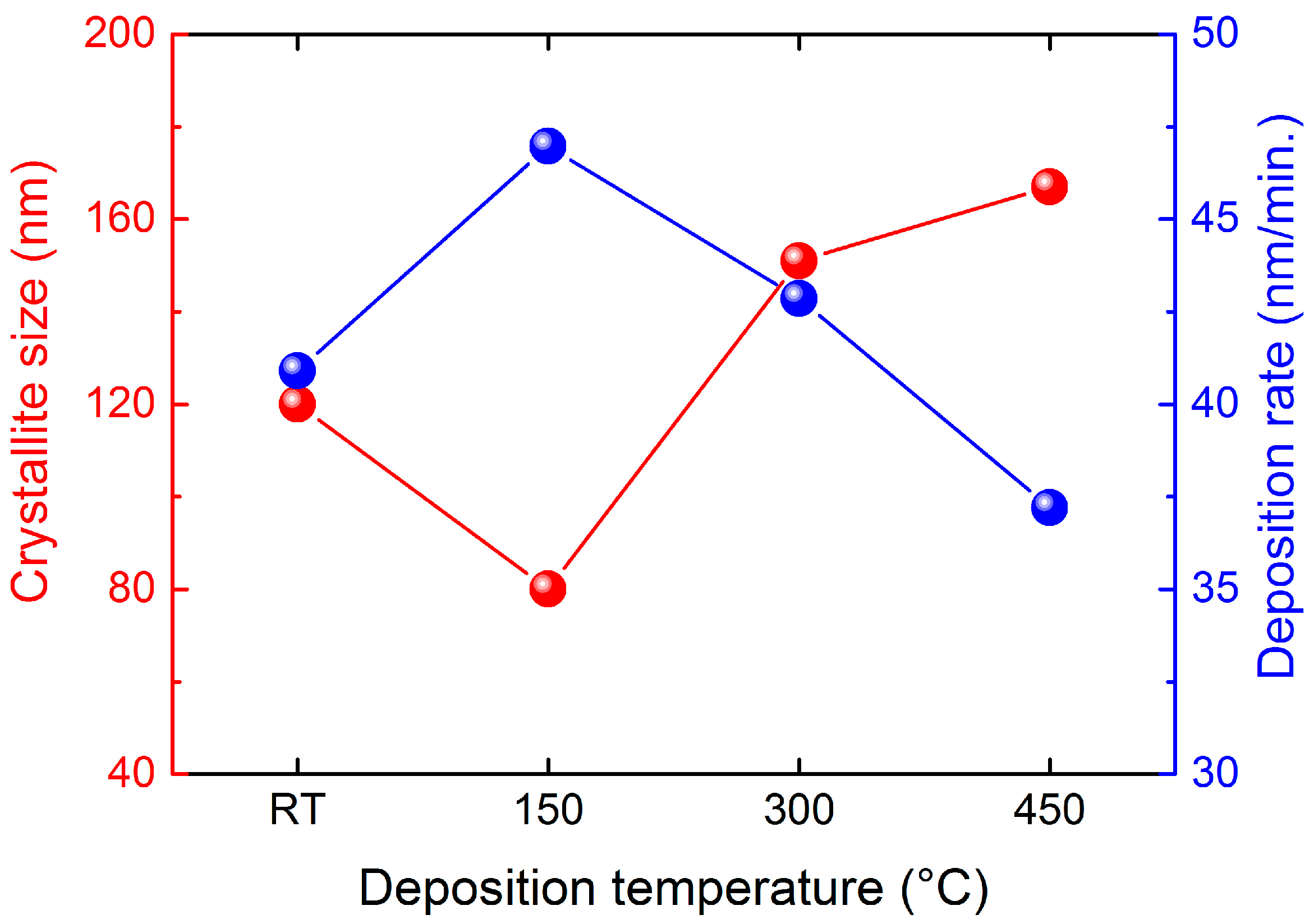
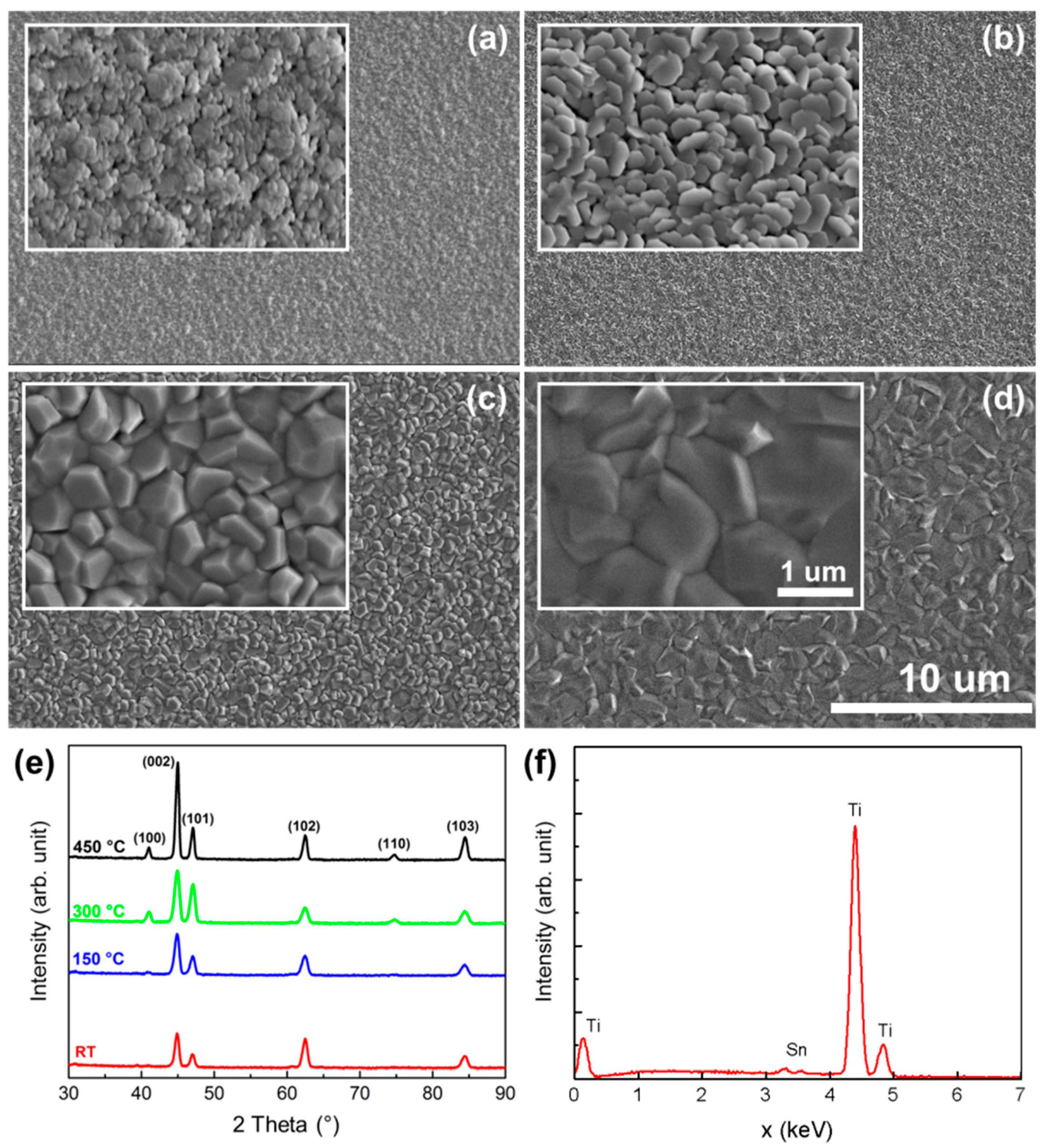
2.1. Structure and Morphology of Sputtered Ti Films

Titanium films were sputtered onto fluorine-doped tin oxide (FTO) substrate at different temperatures such as room temperature (RT), 150 °C, 300 °C, and 450 °C. For the sake of clarity, despite the fact that the RT condition did not include intentional heating, the substrate’s temperature slightly rose up to 80 °C due to the bombardment of the FTO surface by plasma discharge ions. The deposition rate follows a volcano-shaped trend with increasing the deposition temperature and reaches the maximum of 47 nm/min for 150 °C (Figure 1). The grain size follows an opposite trend and the minimum value of ~80 nm is reached for the Ti sample deposited at 150 °C. This dependence can be ascribed to the processes occurring during the sputtering deposition such as extent of shadowing effect at low deposition temperatures, and surface and volume diffusion of condensing atoms at higher temperatures in accordance with the structure zone models [33].
The as-deposited titanium samples were well adherent to the FTO substrate regardless of the temperature used without any visually observable defects. The morphological images of all deposited films are displayed in the scanning electron microscopy (SEM) micrographs reported in Figure 2a–d. With increasing temperature, the shape of grains and their size distribution varied considerably: Ti films deposited at RT showed globular morphology, while fully developed hexagonal platelets with sharp edges were clearly seen for the film deposited at 150 °C. The platelets were randomly distributed and placed on top of each other. The change of morphology is associated with a decrease of the crystallite size from 120 nm (RT) to 80 nm (150 °C) as summarized in Table 1 and Figure 1. Further increase of the deposition temperature led to a higher surface and bulk diffusivity of sputtered atoms promoting formation of angular grains, especially for film deposited at 450 °C, thus leading to a substantial increase of crystallite size (see Table 1).
X-ray diffraction was used to determine the crystalline structures of deposited Ti films. Irrespective of the deposition temperature, the as-prepared films exhibited a variation of peak intensities corresponding to hexagonal polycrystalline structure of titanium with preferential orientation along the (002) crystalline plane that is generally the densest plane for hexagonal close packed structures. It is worth noting the evolution of (100) and (110) peaks with the increase of the deposition temperature in agreement with previous work [34]. The development of these crystalline planes may be attributed to the presence of a compressive stress induced in the films’ microstructure [34,35]. Crystallite size was estimated by using the Scherrer’s equation and retrieved values are shown in Table 1. Figure 2f shows the energy dispersive X-ray spectroscopy (EDS) spectrum of the titanium film deposited at 150 °C on FTO glass. The SEM-EDS analysis revealed traces of Sn in all samples (not shown here) due to the presence of Sn ions into the FTO (i.e., F-doped SnO2) underneath substrate. The surface roughness (Ra) of deposited Ti layers was tested by contact profilometry and the obtained values of standard Ra parameters are provided in Table 1. Surprisingly, the smoothest surface was identified for the films composed of the biggest crystalline size. It was also visually observable as a very flat mirror-like surface. Film thickness obtained from profilometry measurements ranges from 1.35 to 1.60 μm, thus being comparable for all Ti films.

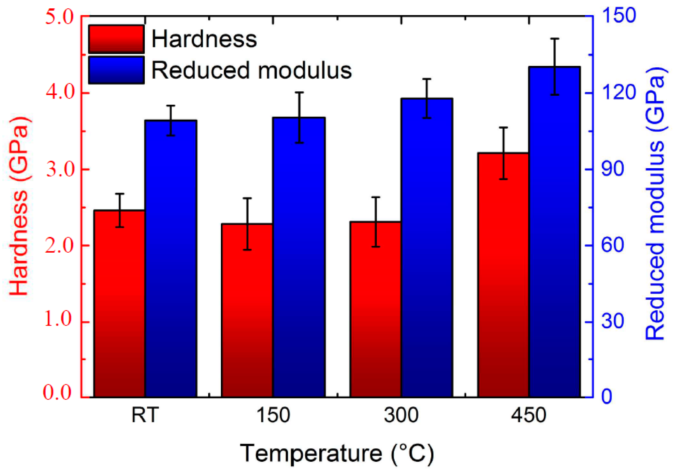
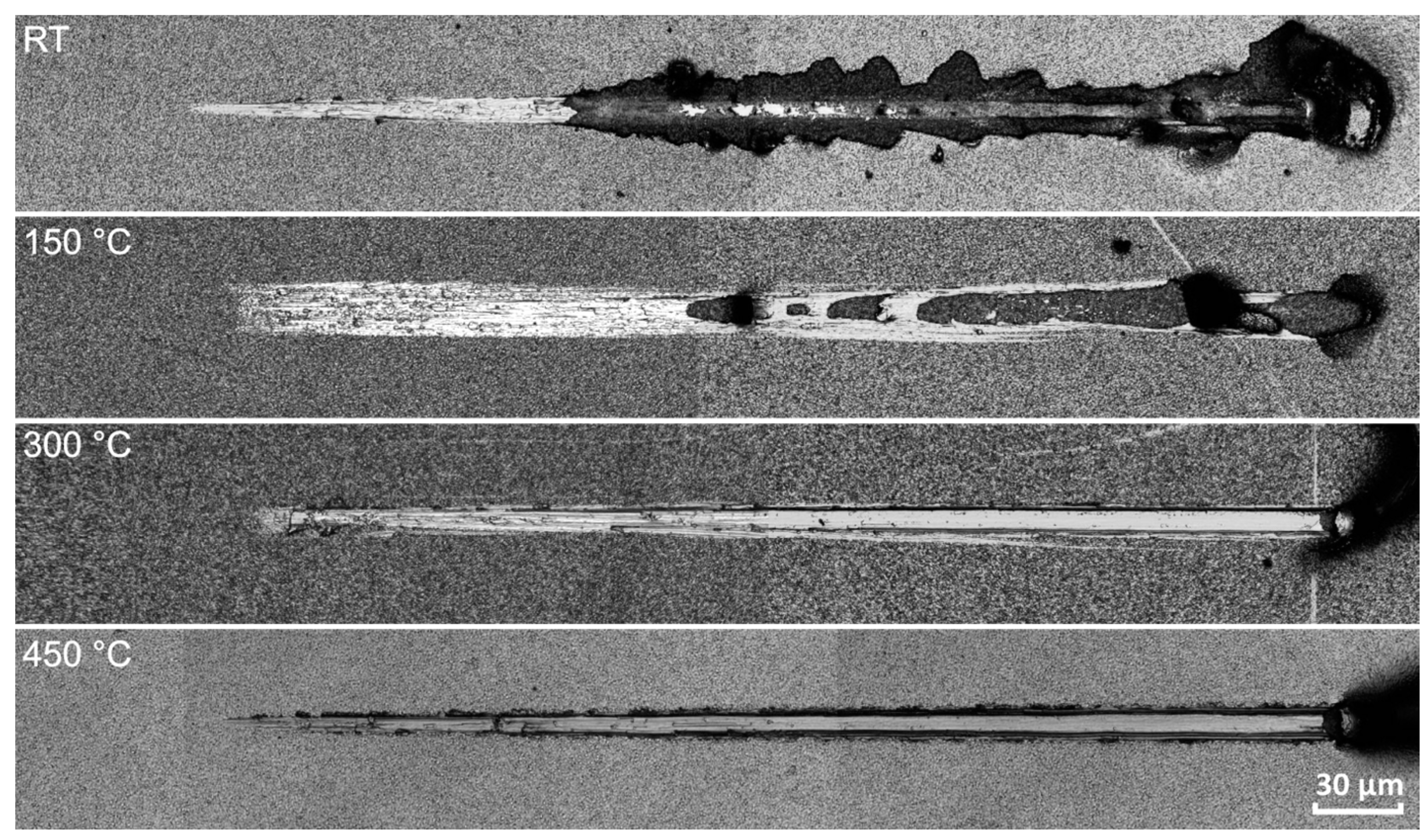
2.2. Mechanical Properties of Sputtered Titanium Films

Analysis of nanoindentation data (Figure 3) evidenced significant differences in mechanical properties between the deposited Ti films. Substrate heating led to an increase in reduced modulus from 109 GPa for RT sample (and similar values observed for 150 and 300 °C) to 130 GPa for the film deposited at 450 °C. Similarly, hardness values are almost the same regardless of the deposition temperature up to 300 °C (~3.75 GPa), while a small increase can be observed for the film deposited at 450 °C. Nanoindentation hardness of the films is only slightly higher in comparison to the coarse grained Ti bulk sheet (~2 GPa) measured at the same experimental setup, especially for the films deposited up to 300 °C. This fact correlates well with the fine-grained structure, where dislocation activity for crystallite with size around 100 nm is suppressed as explained by the well know Hall–Petch effect [36]. Nevertheless, the relative proximity of hardness values of the Ti films and pure Ti metal bulk reflects the high purity of the films, since oxygen or nitrogen impurities strongly affect the mechanical properties and increase both the hardness and elastic modulus values [32]. No traces of oxygen were detected using EDS. Hardness increase up to 4 GPa was reported for Ti sputtered films under similar conditions but under Ar/O2 gas mixture [18]. It should be noted that either oxides (TiO2) or nitrides (TiNx) can reach much higher hardness. In case of magnetron sputtered TiO2 films hardness values of pure anatase is in the range of 6–11 GPa, whereas rutile can reach around 20 GPa [37].
Progressive load scratch tests revealed increasing endurance of Ti films with the increase of deposition temperature, as demonstrated from the residual grooves tracks shown in Figure 4. Sample deposited without applying external heating (RT) exhibits full coating delamination starting from 1/3 of the scratch track. Large spalled areas uncovering the bare substrate, far beyond the residual groove, show that coating-to-substrate adhesion as well as cohesion strength are weak and become a main reason for the system failure. Substrate heating up to 150 °C led to better adhesion, as no delamination is observed and coating is scratched through after approximately half of the scratch track. Deposition temperature of 300 °C and especially 450 °C has a significant impact on scratch resistance as coatings were not scratched through. The residual scratch tracks’ surface morphologies are almost smooth and dominated by plastic deformation (see beginnings of the scratches). This is in accordance with the high level of plasticity index of approx. 83%, defined as the ratio of the plastic work to total indentation work. With increasing load, formation of faint pile up around the wear track occurs. Only slightly worn particle packing is observed at the sides of the wear track. It should be noted that findings of scratch test performed at lower maximum force of 100 mN coincide with those reported in [18].

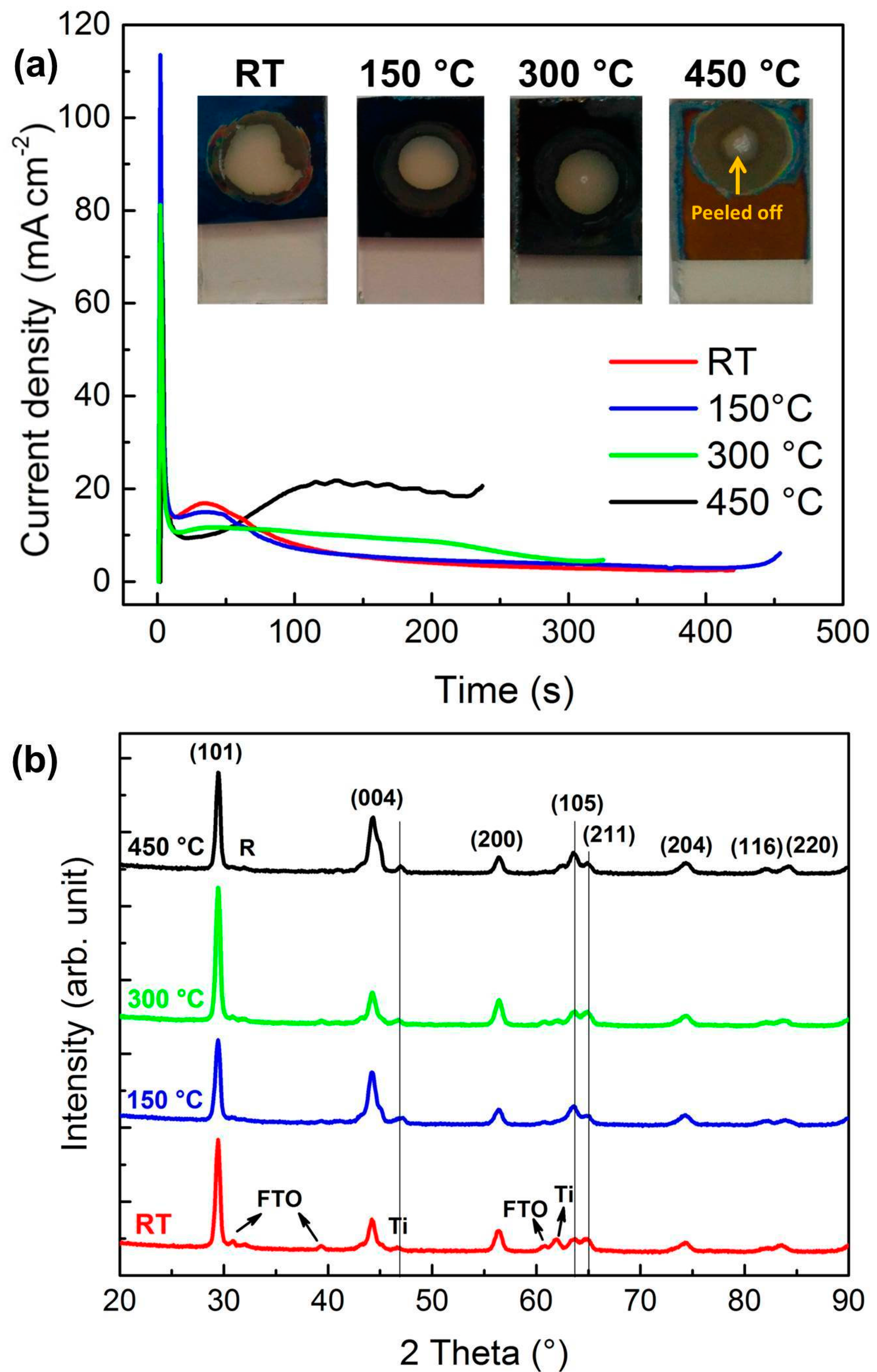
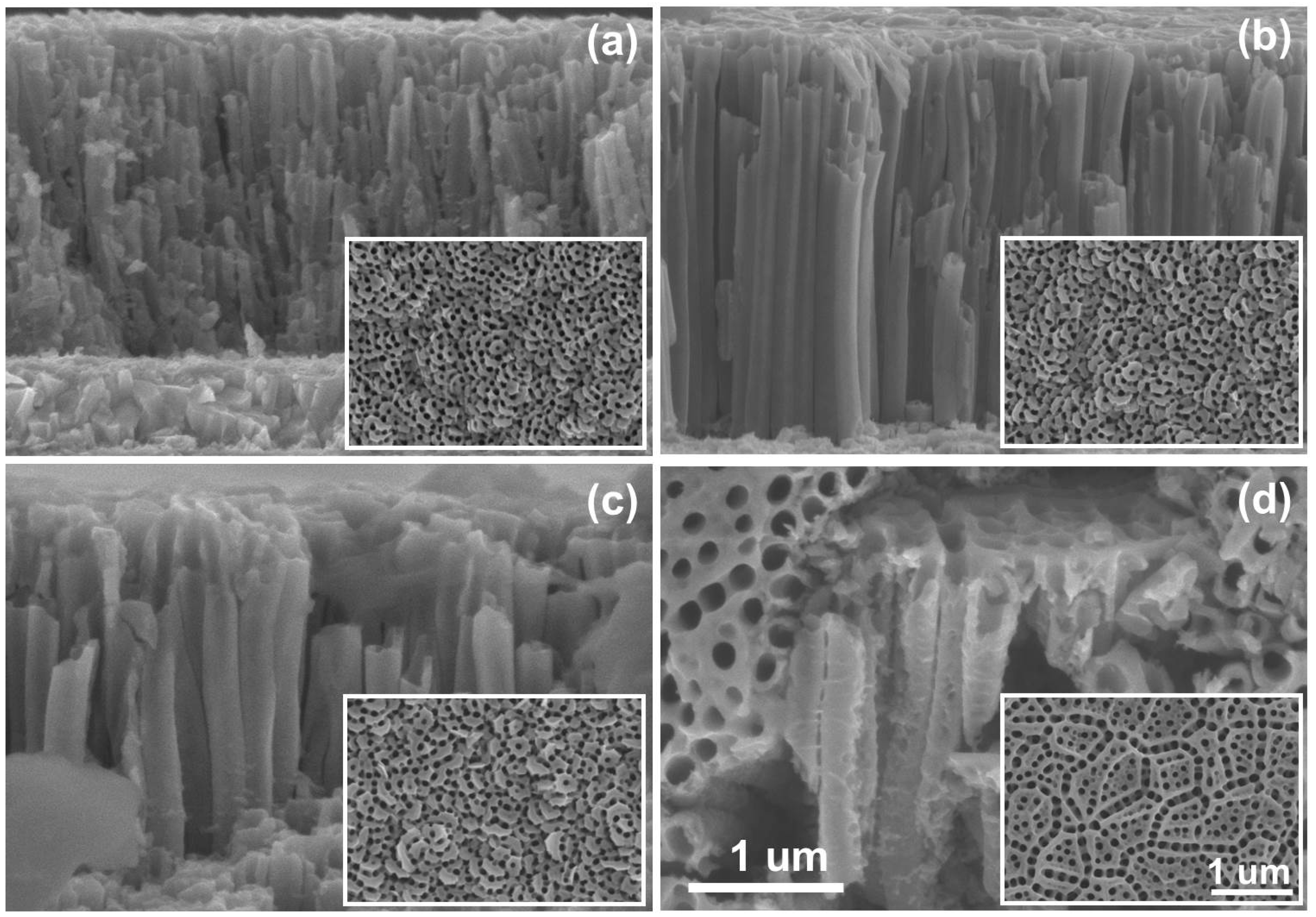
2.3. Electrochemical Anodization to Grow TiO2 Nanotubes

Figure 5a shows the current density plot in time during the anodic oxidation of the sputtered Ti layers sputtered on FTO glass at different temperatures (RT, 150, 300 and 450 °C). All the current transient curves can be divided into three typical stages, already described in detail elsewhere [16,38]. Briefly, the very sharp current density peak observed during the first seconds of the anodization process is associated with the formation of an initial compact TiO2 layer. A relatively steady state region followed, denoting the self-organizing electrochemical reaction underlying the formation of TiO2 nanotubes. Finally, a sudden increase of current density marks the end point of the reaction, which may be accompanied with the creation of random cracks within the TNT and/or their partial delamination [39].
Notably, two trends can be observed when the current density curves are compared. The titanium films deposited at higher temperature required higher current density to be anodically oxidized, while electrochemical reaction lasted for a much shorter time than the titanium films prepared under lower temperature. Due to the elevated temperatures, the crystallite size and density of layers are significantly increased, along with a change in crystallite preferential orientation towards the (002) planes. The shorter the anodization duration the larger the crystallite sizes; at the same time the denser the films the higher current density is required for TNT formation. Interestingly, the TNT peeled off in the center of the anodized area only for the 450 °C sample (Figure 5a). The photographs were captured after the thermal annealing of the as-grown amorphous TiO2 nanotubes in air at 500 °C for 1 h to obtain the crystalline structure. The delamination already occurred during the anodization process despite thermal annealing. It should be noted that the dominant (002) plane is the one with the highest thermally induced strain energy per unit volume [40]. Taking into account the crystallographic planes observed in Figure 2e, the strain energy decreases in the following order (002), (103), (102), (101), (100) and (110), where the last two are equal [40]. Hence, the problematic anodization of the film deposited at 450 °C stems from the combination of high current density (high thermal load) during anodization and the highest thermally induced strains of the film’s dominant (002) plane.
XRD spectra of the thermally annealed TiO2 nanotubes show only characteristic peaks related to the polycrystalline anatase phase (Figure 5b). The crystallite size, obtained through the Sherrer equation, followed the same trend as observed for titanium films, i.e., the smallest grain size of 14 nm was revealed for the TNT grown from the titanium films deposited at 150 °C, while with the increase of the deposition temperature the grain sizes increased up to 87 nm for 450 °C. In the diffractograms, the signals related to metallic titanium as well as the cassiterite (SnO2) of the FTO substrate were detected. The source of Ti signal is probably due to the side unanodized parts of the samples rather than residual Ti impurities in the TNTs.
The cross-sectional and surface SEM morphology images of the prepared nanotubes are shown in Figure 6. The anodization formed self-organized arrays of highly transparent nanotubes grown vertically on the FTO substrate. All the prepared nanotubes had a similar thickness of 3 µm, which corresponds to a volume expansion factor of ~2 due to the anodization procedure. This value is in agreement with findings from Albu and Schmuki, describing how key parameters such as content of water in the electrolyte and overall anodization potential influence the expansion factor of TNTs [41]. The surface SEM images (see inserts in Figure 6) are very similar for RT, 150 °C, and 300 °C deposited Ti films. The similarity is due to a nanoporous thin initiation layer which is always present at the top of nanotubes due to the TiO2 layer formed at the first stage of the anodization process (see description above). By comparing these three types of nanotube arrays a widening of the tube diameters can be indicated. The surface morphology is slightly different for the film deposited at 450 °C. In this case, pores with higher diameters are formed at edges of the very large titanium grains (see Figure 2d and Figure 6d) [39]. The highest quality of nanotubes in terms of homogeneity, degree of organization, smoothness, and compactness was observed for the TNT grown from Ti films deposited at 150 °C. A much higher number of defects was observed for the TNT grown from RT and 300 °C titanium films. For comparison, the parts of TNT made from Ti films deposited at 450 °C, which were not delaminated from the FTO substrate are also shown. The very low quality of these nanotubes is mainly due to numerous cracks and is evident (Figure 6d).

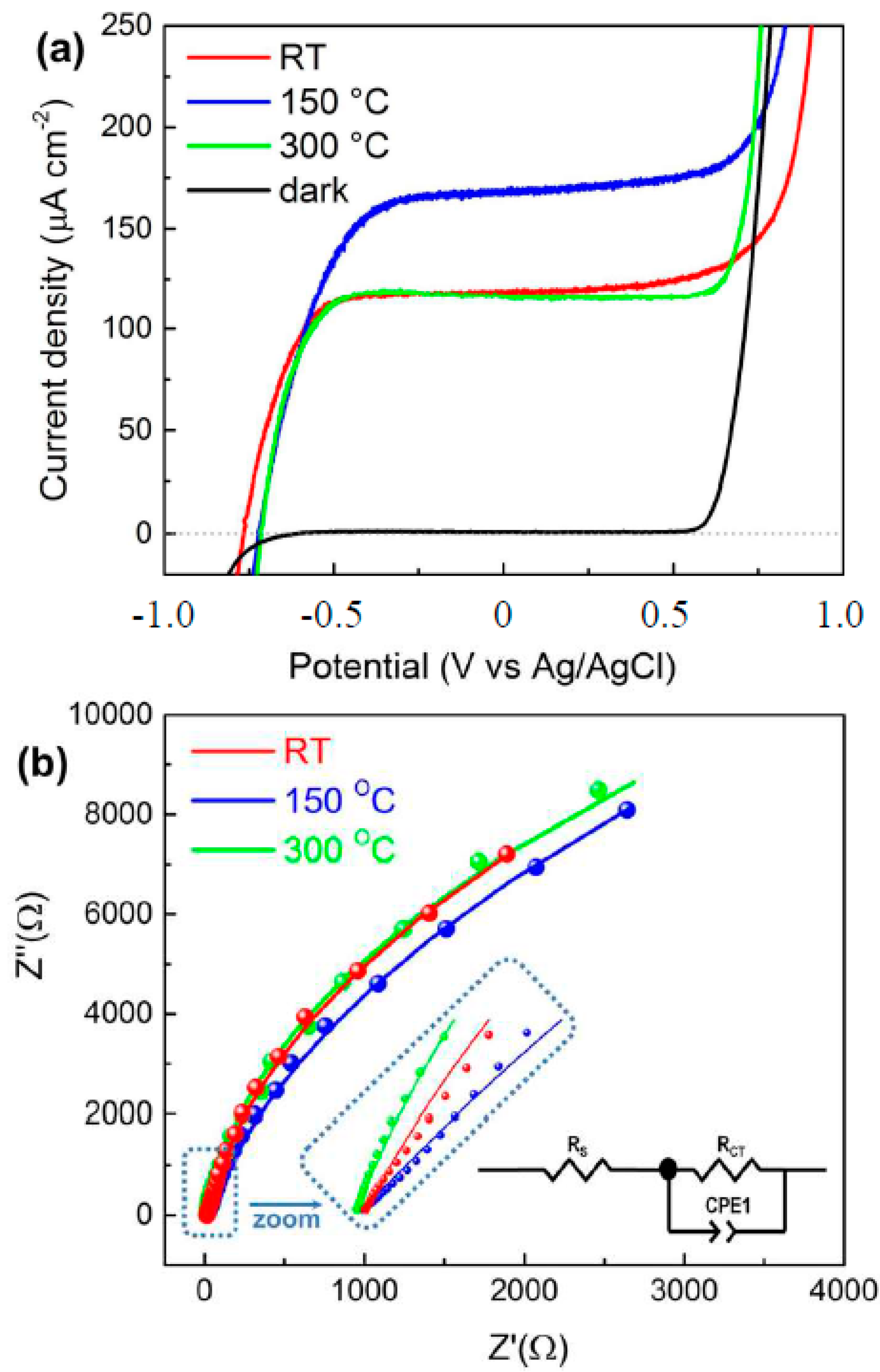
2.4. Photoelectrochemical Measurements

Photoelectrochemical properties were investigated based on linear sweep voltammetry and electrochemical impedance spectroscopy (EIS) measurements. The polarization curves showing the dependence of current density on applied potential are presented in Figure 7a. The performance of TNT obtained from Ti film sputtered at 450 °C was not measured due to the collapse of the structure upon air annealing. The experiments were carried out in a conventional three-electrode configuration in 1 M NaOH and under standard AM1.5G (intensity 100 mW/cm2) illumination. All three measured photoanodes showed a similar voltammetry profile characterized by an onset potential at ~0.74 V vs. Ag/AgCl and reaching a photocurrent plateau. From the polarization curves (see Figure 7a), the photocurrent density at 0.5 V (at the end point of the steady-state plateau-like photocurrents and before the electrochemical oxygen evolution onset potential) are as follows: 175 μA cm−2, 125 μA cm−2, and 116 μA cm−2 for 150 °C, RT, and 300 °C TNT photoanodes, respectively. The highest photocurrent value obtained for the sample TNT-150 can be ascribed to the smallest crystallite size, the defect-free morphology of high quality nanotubes for the 150 °C sample.
To investigate the reasons underlying the photocurrent trend, we carried out EIS measurements under AM1.5G illumination at 0 V vs. Ag/AgCl (Figure 7b). The semicircular arch diameter indicates the charge transfer ability of the examined photoelectrode. To extract the charge transfer parameters associated with EIS curves, we fitted the curves with an equivalent Randle’s circuit (see inset of Figure 7b), where Rs is the series/solution resistance, RCT is the charge transfer resistance, and CPE1 is the constant phase element (capacitance) of semiconductor/electrolyte interface. The fitted parameters for each sample are shown in Table 2. Rs slightly decreases with increasing temperature of Ti sputtered films and shows comparable values. The double layer capacitance CPE1 is higher for TNT-RT due to higher accumulation of charge at the electrode/electrolyte interface; it may be because of grain size differences or accumulation of more charges at the grain boundaries of the sample. The charge transfer resistance RCT for TNT-150 sample is 33.7 kΩ, lower compared to TNT-RT (39.7 kΩ) and TNT-300 (36.4 kΩ) suggesting a higher charge transfer rate at the semiconductor/electrolyte interface that, thus, underlies the observed enhancement in the photocurrent.

3. Experimental

3.1. Deposition of Titanium Films by Magnetron Sputtering

Titanium thin films, with thickness of ~1.5 μm, were deposited by pulsed DC magnetron sputtering of the titanium target (size of 4“ and purity of 99.995%) on a commercially available FTO coated glasses substrates (Solaronix, Aubonne, Switzerland) with dimensions of 25 × 15 × 2 mm. A standardized three-step cleaning protocol was used before film deposition. rinsing the substrates in an ultrasound bath in acetone, ethanol and distilled water, each step lasting 5 min. Subsequent drying at RT was applied to remove residual water from the glass samples. The chamber was evacuated to the base pressure of 1 × 10⁻⁴ Pa. The depositions were performed at a pressure of 0.2 Pa for 240 min on unheated as well as heated substrates at various temperatures of 150, 300 and 450 °C. Although no intentional heating was applied the substrate temperature increased up to 90 °C during deposition as a result of its interaction with plasma. The DC power of 700 W (power density of 8.6 W/cm2) was applied in a pulsed mode at pulse frequency of 50 kHz and duty cycle of 50%. Prior the deposition a substrate pre-treatment was employed. First the substrate surfaces were cleaned using radio frequency (RF) (13.56 MHz) plasma etching in argon and then activated in the RF discharge in the mixture 50:50 of Ar and forming gas (10% of H2 and 90% of N2). The RF power of 130 W was typically used.

3.2. Mechanical and Tribological Properties

Mechanical and tribological characteristics were explored using a fully calibrated NanoTest instrument (MicroMaterials, Wrexham, UK) in a load-controlled mode. Nanoindentation at a peak force of 3 mN with a diamond pyramidal Berkovich indenter was employed for hardness and elastic modulus measurement [42,43]. The indentation curves were analyzed using the standard method [44].
Sphero-conical Rockwell indenter with a nominal radius of 10 µm was used for scratch test to assess the adhesion-cohesion properties of the films. During the standard scratch procedure, the initially constant topographic load of 0.02 mN was applied over the first 50 μm and then ramped to 500 mN at constant loading rate of 13 mN/s to initiate films failure and reveal their cohesive and/or adhesive limits. Evaluation of the scratch test was performed on the basis of the indenter on-load depth record and analysis of the residual scratch tracks. Laser scanning confocal microscope LEXT OLS 3100 (Olympus, Tokyo, Japan) was used for high-resolution imaging.

3.3. Electrochemical Anodization to Grow Self-Organized TiO2 Nanotubes

The titanium films on FTO glass were washed with ethanol. TiO2 nanotubes were then grown at 60 V using a power source (STATRON 3253.3, Statron AG, Mägenwil, Switzerland) in a two-electrode configuration with a counter electrode made of platinum (cathode) and the working electrode was the titanium film (anode). The electrolyte contained 0.2 mol dm−3 NH4F and 4 mol dm−3 H2O in ethylene glycol. After the anodization process, the samples were washed in ethanol and then dried in a nitrogen stream. The as-prepared amorphous TNT were annealed at 500 °C for 1h in air using cylindrical furnace (Clasic CLARE 4.0, CLASIC, Revnice, Czech Republic) with temperature increase 5 °C min−1 to obtain the crystalline phase. The nanotubes grown from titanium films deposited at different temperatures such as RT, 150 °C, 300 °C, and 450 °C, are in the text coded as TNT-RT, TNT-150, TNT-300, and TNT-450, respectively.

3.4. Characterization of the Titanium Films and TiO2 Nanotubes

Structure of the Ti films was determined using the Empyrean (PANalytical, Almelo, The Netherlands) diffractometer equipped with Co. radiation source, focusing mirror, and Pixcell detector via grazing angle regime with incident angle 2°. Mean crystallite size was determined using the Scherrer equation. Surface of the films and its cross-sections were observed using Scanning Electron Microscope Hitachi SU6600 (Hitachi, Tokyo, Japan).

3.5. Photoelectrochemistry

The photoelectrochemical data were collected using a standard three-electrode electrochemical cell with a Gamry Series G 300 Potentiostat (Warminster, PA, USA). The TiO2 nanotubes served as working electrode (photoanode), the Ag/AgCl (3 M KCl) as the reference electrode and the Pt wire was used as the counter electrode. A 150 W Xenon lamp coupled with an AM1.5G filter was used as a light source. The power intensity was kept at 1 sun (100 mW/cm2) which was calibrated though a silicon reference solar cell (Newport Corporation, Irvine, CA, USA). The photoelectrochemical behavior of prepared electrodes was investigated by means of linear sweep voltammetry measurements in 1 M NaOH electrolyte (pH 13.5). The electrochemical impedance spectroscopy (EIS) data were recorded using a Gamry instrument (ESA 410, Gamry, Warminster, PA, USA) in the frequency range from 0.1 Hz to 100 kHz under 1 sun illumination at a bias of 0 V vs. Ag/AgCl. At least three electrodes of each type were fabricated and tested. All electrodes showed similar J-V curves, and representative data are reported.

4. Conclusions

In this study, we have reported a detailed investigation of mechanical and adhesion properties of Ti films sputtered at different temperatures, showing that temperatures as high as 450 °C produce Ti films with well-defined platelet texture and with best mechanical and adhesion properties. However, we have found that these different sputtering conditions strongly influence crystallographic and photoelectrochemical water spitting activity of self-organized TiO2 nanotubes grown from Ti films. The more active TiO2 nanotube sample towards photoelectrochemical water splitting was obtained from Ti substrate sputtered at 150 °C showing the lowest crystallite size, best degree of self-organization, and enhanced charge transfer at the semiconductor/liquid interface. This work remarks the challenge behind achieving highly active and durable materials for photonics applications and shows that advanced magnetron sputtering may enable good control over microstructural properties and, thus, performance of semiconductor thin films.

Acknowledgments

The authors gratefully acknowledge the support by the Operational Programme Research, Development and Education—European Regional Development Fund, project no. CZ.02.1.01/0.0/0.0/15_003/0000416 and the project 8E15B009 of the Ministry of Education, Youth and Sports of the Czech Republic. The authors also acknowledge the financial support from Grant Agency of Czech Republic (project number 15-19705S and 17-20008S) and the Internal Grant of Palacky University (IGA_PrF_2017_005).

Author Contributions

S.K. and Z.H. conceived and designed the experiments; M.Z., R.C., H.K., S.P., J.T., Y.R., A.N., J.K. performed the experiments, analyzed the data and contributed reagents/materials/analysis tools; M.Z., R.C., S.K., A.N. wrote the paper, P.S. and R.Z. supervised the project.

Conflicts of Interest

The authors declare no conflicts of interest.

References

  1. Papoutsi, D.; Lianos, P.; Yianoulis, P.; Koutsoukos, P. Sol-gel derived TiO2 microemulsion gels and coatings. Langmuir 1994, 10, 1684–1689. [Google Scholar] [CrossRef]
  2. Kment, S.; Kmentova, H.; Kluson, P.; Krysa, J.; Hubicka, Z.; Cirkva, V.; Gregora, I.; Solcova, O.; Jastrabik, L. Notes on the photo-induced characteristics of transition metal-doped and undoped titanium dioxide thin films. J. Colloid Interface Sci. 2010, 348, 198–205. [Google Scholar] [CrossRef] [PubMed]
  3. Krysa, J.; Zlamal, M.; Kment, S.; Brunclikova, M.; Hubicka, Z. TiO2 and Fe2O3 films for photoelectrochemical water splitting. Molecules 2015, 20, 1046. [Google Scholar] [CrossRef] [PubMed]
  4. Kment, S.; Kluson, P.; Stranak, V.; Virostko, P.; Krysa, J.; Cada, M.; Pracharova, J.; Kohout, M.; Morozova, M.; Adamek, P.; et al. Photo-induced electrochemical functionality of the TiO2 nanoscale films. Electrochim. Acta 2009, 54, 3352–3359. [Google Scholar] [CrossRef]
  5. Naldoni, A.; Riboni, F.; Marelli, M.; Bossola, F.; Ulisse, G.; Di Carlo, A.; Pis, I.; Nappini, S.; Malvestuto, M.; Dozzi, M.V.; et al. Influence of TiO2 electronic structure and strong metal-support interaction on plasmonic au photocatalytic oxidations. Catal. Sci. Technol. 2016, 6, 3220–3229. [Google Scholar] [CrossRef]
  6. Chen, X.; Mao, S.S. Titanium dioxide nanomaterials:  Synthesis, properties, modifications, and applications. Chem. Rev. 2007, 107, 2891–2959. [Google Scholar] [CrossRef] [PubMed]
  7. Kavan, L.; Grätzel, M.; Rathouský, J.; Zukalb, A. Nanocrystalline TiO2 (anatase) electrodes: Surface morphology, adsorption, and electrochemical properties. J. Electrochem. Soc. 1996, 143, 394–400. [Google Scholar] [CrossRef]
  8. Naldoni, A.; Montini, T.; Malara, F.; Mróz, M.M.; Beltram, A.; Virgili, T.; Boldrini, C.L.; Marelli, M.; Romero-Ocaña, I.; Delgado, J.J.; et al. Hot electron collection on brookite nanorods lateral facets for plasmon-enhanced water oxidation. ACS Catal. 2017, 7, 1270–1278. [Google Scholar] [CrossRef]
  9. Ren, L.; Li, Y.; Hou, J.; Zhao, X.; Pan, C. Preparation and enhanced photocatalytic activity of TiO2 nanocrystals with internal pores. ACS Appl. Mater. Interfaces 2014, 6, 1608–1615. [Google Scholar] [CrossRef] [PubMed]
  10. Chen, X.; Shen, S.; Guo, L.; Mao, S.S. Semiconductor-based photocatalytic hydrogen generation. Chem. Rev. 2010, 110, 6503–6570. [Google Scholar] [CrossRef] [PubMed]
  11. Ma, Y.; Wang, X.; Jia, Y.; Chen, X.; Han, H.; Li, C. Titanium dioxide-based nanomaterials for photocatalytic fuel generations. Chem. Rev. 2014, 114, 9987–10043. [Google Scholar] [CrossRef] [PubMed]
  12. Straňák, V.; Čada, M.; Quaas, M.; Block, S.; Bogdanowicz, R.; Kment, S.; Wulff, H.; Hubička, Z.; Helm, C.A.; Tichý, M.; et al. Physical properties of homogeneous TiO2 films prepared by high power impulse magnetron sputtering as a function of crystallographic phase and nanostructure. J. Phys. D: Appl. Phys. 2009, 42, 105204. [Google Scholar] [CrossRef]
  13. Roy, P.; Berger, S.; Schmuki, P. TiO2 nanotubes: Synthesis and applications. Angew. Chem. Int. Ed. 2011, 50, 2904–2939. [Google Scholar] [CrossRef] [PubMed]
  14. Gordon, T.R.; Cargnello, M.; Paik, T.; Mangolini, F.; Weber, R.T.; Fornasiero, P.; Murray, C.B. Nonaqueous synthesis of TiO2 nanocrystals using TiF4 to engineer morphology, oxygen vacancy concentration, and photocatalytic activity. J. Am. Chem. Soc. 2012, 134, 6751–6761. [Google Scholar] [CrossRef] [PubMed]
  15. Dong, F.; Zhao, W.; Wu, Z. Characterization and photocatalytic activities of C, N and S co-doped TiO2 with 1D nanostructure prepared by the nano-confinement effect. Nanotechnology 2008, 19, 365607. [Google Scholar] [CrossRef] [PubMed]
  16. Kment, S.; Riboni, F.; Pausova, S.; Wang, L.; Wang, L.; Han, H.; Hubicka, Z.; Krysa, J.; Schmuki, P.; Zboril, R. Photoanodes based on TiO2 and α-Fe2O3 for solar water splitting—Superior role of 1D nanoarchitectures and of combined heterostructures. Chem. Soc. Rev. 2017, 46, 3716–3769. [Google Scholar] [CrossRef] [PubMed]
  17. Paramasivam, I.; Jha, H.; Liu, N.; Schmuki, P. A review of photocatalysis using self-organized TiO2 nanotubes and other ordered oxide nanostructures. Small 2012, 8, 3073–3103. [Google Scholar] [CrossRef] [PubMed]
  18. Krysa, J.; Lee, K.; Pausova, S.; Kment, S.; Hubicka, Z.; Ctvrtlik, R.; Schmuki, P. Self-organized transparent 1D TiO2 nanotubular photoelectrodes grown by anodization of sputtered and evaporated ti layers: A comparative photoelectrochemical study. Chem. Eng. J. 2017, 308, 745–753. [Google Scholar] [CrossRef]
  19. Fahim, N.F.; Sekino, T.; Morks, M.F.; Kusunose, T. Electrochemical growth of vertically-oriented high aspect ratio titania nanotubes by rabid anodization in fluoride-free media. J. Nanosci. Nanotechnol. 2009, 9, 1803–1818. [Google Scholar] [CrossRef] [PubMed]
  20. Kmentova, H.; Kment, S.; Wang, L.; Pausova, S.; Vaclavu, T.; Kuzel, R.; Han, H.; Hubicka, Z.; Zlamal, M.; Olejnicek, J.; et al. Photoelectrochemical and structural properties of TiO2 nanotubes and nanorods grown on FTO substrate: Comparative study between electrochemical anodization and hydrothermal method used for the nanostructures fabrication. Catal. Today 2017, 287, 130–136. [Google Scholar] [CrossRef]
  21. Lee, K.; Kim, D.; Berger, S.; Kirchgeorg, R.; Schmuki, P. Anodically formed transparent mesoporous TiO2 electrodes for high electrochromic contrast. J. Mater. Chem. 2012, 22, 9821–9825. [Google Scholar] [CrossRef]
  22. Macak, J.M.; Schmuki, P. Anodic growth of self-organized anodic TiO2 nanotubes in viscous electrolytes. Electrochim. Acta 2006, 52, 1258–1264. [Google Scholar] [CrossRef]
  23. Zwilling, V.; Aucouturier, M.; Darque-Ceretti, E. Anodic oxidation of titanium and TA6V alloy in chromic media. An electrochemical approach. Electrochim. Acta 1999, 45, 921–929. [Google Scholar] [CrossRef]
  24. Paušová, Š.; Kment, Š.; Zlámal, M.; Baudys, M.; Hubička, Z.; Krýsa, J. Transparent nanotubular TiO2 photoanodes grown directly on fto substrates. Molecules 2017, 22, 775. [Google Scholar] [CrossRef] [PubMed]
  25. Berger, S.; Ghicov, A.; Nah, Y.C.; Schmuki, P. Transparent TiO2 nanotube electrodes via thin layer anodization: Fabrication and use in electrochromic devices. Langmuir 2009, 25, 4841–4844. [Google Scholar] [CrossRef] [PubMed]
  26. Krýsa, J.; Zlámal, M.; Paušová, Š.; Kotrla, T.; Kment, Š.; Hubička, Z. Hematite photoanodes for solar water splitting: Directly sputtered vs. Anodically oxidized sputtered Fe. Catal. Today 2017, 287, 99–105. [Google Scholar] [CrossRef]
  27. Sadek, A.Z.; Zheng, H.; Latham, K.; Wlodarski, W.; Kalantar-zadeh, K. Anodization of Ti thin film deposited on ito. Langmuir 2009, 25, 509–514. [Google Scholar] [CrossRef] [PubMed]
  28. Tang, Y.; Tao, J.; Zhang, Y.; Wu, T.; Tao, H.; Bao, Z. Preparation and characterization of TiO2 nanotube arrays via anodization of titanium films deposited on fto conducting glass at room temperature. Acta Physico-Chim. Sin. 2008, 24, 2191–2197. [Google Scholar] [CrossRef]
  29. Wang, J.; Wang, H.; Li, H.; Wu, J. Synthesis and characterization of TiO2 nanotube film on fluorine-doped tin oxide glass. Thin Solid Films 2013, 544, 276–280. [Google Scholar] [CrossRef]
  30. Olejníček, J.; Hubička, Z.; Kment, Š.; Čada, M.; Kšírová, P.; Adámek, P.; Gregora, I. Investigation of reactive HiPIMS + MF sputtering of TiO2 crystalline thin films. Surf. Coat. Technol. 2013, 232, 376–383. [Google Scholar] [CrossRef]
  31. Bukauskas, V.; Kaciulis, S.; Mezzi, A.; Mironas, A.; Niaura, G.; Rudzikas, M.; Šimkienė, I.; Šetkus, A. Effect of substrate temperature on the arrangement of ultra-thin TiO2 films grown by a dc-magnetron sputtering deposition. Thin Solid Films 2015, 585, 5–12. [Google Scholar] [CrossRef]
  32. Firstov, S.; Kulikovsky, V.; Rogul, T.; Ctvrtlik, R. Effect of small concentrations of oxygen and nitrogen on the structure and mechanical properties of sputtered titanium films. Surf. Coat. Technol. 2012, 206, 3580–3585. [Google Scholar] [CrossRef]
  33. Petrov, I.; Barna, P.B.; Hultman, L.; Greene, J.E. Microstructural evolution during film growth. J. Vacuum Sci. Technol. A 2003, 21, S117–S128. [Google Scholar] [CrossRef]
  34. Chawla, V.; Jayaganthan, R.; Chawla, A.K.; Chandra, R. Microstructural characterizations of magnetron sputtered Ti films on glass substrate. J. Mater. Process. Technol. 2009, 209, 3444–3451. [Google Scholar] [CrossRef]
  35. Savaloni, H.; Taherizadeh, A.; Zendehnam, A. Residual stress and structural characteristics in Ti and Cu sputtered films on glass substrates at different substrate temperatures and film thickness. Phys. B Condens. Matter 2004, 349, 44–55. [Google Scholar] [CrossRef]
  36. Arzt, E. Size effects in materials due to microstructural and dimensional constraints: A comparative review. Acta Mater. 1998, 46, 5611–5626. [Google Scholar] [CrossRef]
  37. Kulikovsky, V.; Ctvrtlik, R.; Vorlicek, V.; Filip, J.; Bohac, P.; Jastrabik, L. Mechanical properties and structure of TiO2 films deposited on quartz and silicon substrates. Thin Solid Films 2013, 542, 91–99. [Google Scholar] [CrossRef]
  38. Lee, K.; Mazare, A.; Schmuki, P. One-dimensional titanium dioxide nanomaterials: Nanotubes. Chem. Rev. 2014, 114, 9385–9454. [Google Scholar] [CrossRef] [PubMed]
  39. Kuzmych, O. Defect Minimization and Morphology Optimization in TiO2 Nanotube Thin Films, Grown on Transparent Conducting Substrate, for Dye Synthesized Solar Cell Application. Thin Solid Films 2012, 522, 71–78. [Google Scholar] [CrossRef]
  40. Witt, F.; Vook, R.W. Thermally induced strains in diamond cubic, tetragonal, orthorhombic, and hexagonal films. J. Appl. Phys. 1969, 40, 709–719. [Google Scholar] [CrossRef]
  41. Albu, S.P.; Schmuki, P. Influence of anodization parameters on the expansion factor of TiO2 nanotubes. Electrochim. Acta 2013, 91, 90–95. [Google Scholar] [CrossRef]
  42. Ctvrtlik, R.; Al-Haik, M.; Kulikovsky, V. Mechanical properties of amorphous silicon carbonitride thin films at elevated temperatures. J. Mater. Sci. 2015, 50, 1553–1564. [Google Scholar] [CrossRef]
  43. Ctvrtlik, R.; Kulikovsky, V.; Vorlicek, V.; Tomastik, J.; Drahokoupil, J.; Jastrabik, L. Mechanical properties and microstructural characterization of amorphous SiCxNy thin films after annealing beyond 1100 °C. J. Am. Ceram. Soc. 2016, 99, 996–1005. [Google Scholar] [CrossRef]
  44. Oliver, W.C.; Pharr, G.M. An improved technique for determining hardness and elastic modulus using load and displacement sensing indentation experiments. J. Mater. Res. 1992, 7, 1564–1583. [Google Scholar] [CrossRef]
Figure 1. Crystallite size and deposition rate as a function of deposition temperature for the direct current magnetron sputtered Ti films. Deposition rate shows a volcano shape dependence on temperature, while crystallite size has an opposite trend. RT: room temperature.
Catalysts 08 00025 g001
Figure 2. Scanning electron microscope (SEM) images of titanium samples deposited without substrate heating at (a) RT, (b) 150 °C, (c) 300 °C and (d) 450 °C. (e) X-ray diffraction (XRD) spectra of all deposited Ti films; (f) energy dispersive X-ray spectroscopy spectrum of titanium film deposited at 150 °C on fluorine-doped tin oxide (FTO) substrate.
Catalysts 08 00025 g002
Figure 3. Hardness and reduced modulus of the Ti films deposited at different temperatures.
Catalysts 08 00025 g003
Figure 4. Typical scratch tracks for Ti films deposited at temperatures ranging from room temperature (RT) to 450 °C.
Catalysts 08 00025 g004
Figure 5. (a) Current density versus time plot recorder during the electrochemical anodization of titanium films with the pictures of grown and annealed TiO2 nanotubes; (b) XRD spectra of TiO2 nanotubes after thermal annealing at 450 °C for 3 h in air.
Catalysts 08 00025 g005
Figure 6. Cross-sectional and corresponding surface (inserts) SEM images of the TiO2 nanotubes (TNT) arrays grown from titanium films deposited at RT (a), 150 °C (b), 300 °C (c), and 450 °C (d).
Catalysts 08 00025 g006
Figure 7. Linear sweep voltammetry curves of the TiO2 nanotubes (a). Nyquist plots for TNT-RT, TNT-150, and TNT-300 measured at an applied bias potential of 0 V vs. Ag/AgCl under illumination of AM1.5G with the intensity of 100 mW cm−2 (b). Symbols are experimentally measured impedance data; solid curves are fitted to the equivalent circuit shown (inset). Rs is solution resistance, RCT is charge transfer resistance, Constant phase element (CPE1) is capacitance element. Photoelectrochemical (PEC) measurements were carried out in 1 M NaOH electrolyte under simulated solar light irradiation (air mass-AM1.5G, 100 mW/cm2).
Catalysts 08 00025 g007
Table 1. Thickness and roughness from profilometry of Ti films; crystallite size of the deposited Ti films and anodized TiO2 nanotubes. RT: room temperature.
Temperature, °CThickness, µmRoughness, µmCrystallite Size Ti, nmCrystallite Size TiO2, nm
RT1.350.08012039
1501.610.1258014
3001.500.11815125
4501.480.02816787
Table 2. Electrochemical Impedance spectroscopy data from measurement taken at 0 V vs. Ag/AgCl under 1 sun illumination.
SampleRS, ΩRCT, ΩCPE1, µF
RT16.7139,799 ± 1149201 ± 0.57
15015.7033,698 ± 279172 ± 0.33
30013.3736,430 ± 841165 ± 0.44

