Article

Effects of Nanoscaled Tin-Doped Indium Oxide on Liquid Crystals against Electrostatic Discharge

1
Department of Electrical Engineering, Feng Chia University, 100 Wenhwa Rd., Seatwen, Taichung 40724, Taiwan
2
Department of Electronic Engineering, Feng Chia University, 100 Wenhwa Rd., Seatwen, Taichung 40724, Taiwan
3
Department of Materials Science and Engineering, Feng Chia University, 100 Wenhwa Rd., Seatwen, Taichung 40724, Taiwan
*
Author to whom correspondence should be addressed.
Crystals 2013, 3(4), 530-553; https://doi.org/10.3390/cryst3040530
Submission received: 2 July 2013 / Revised: 11 September 2013 / Accepted: 28 October 2013 / Published: 26 November 2013

Abstract

:
In our studies, it was confirmed that the cause of image sticking on liquid crystal (LC) cells is based on attacks of electrostatic discharge (ESD), which can be greatly relieved by doping with a small amount of tin-doped indium oxide (ITO) nanoparticles. Our proposed remedy allows the residual time of image sticking to be significantly reduced by more than an order and may protect the LC displays against any adverse ESD conditions, thus enhancing the overall display quality and reliability. In this study, conventional voltage-transmittance (V-T) characterization, voltage holding ratio (VHR) measurement, and ESD testing were employed to investigate the properties of the ITO-doped LCs. Based on our low voltage measurement results, it is interesting to find that ITO nanoparticles do not evidently alter the intrinsic properties of the LC. Namely, ITO additive initiates an early breakdown of the doped LC samples exposed to high electric fields. A model is proposed in this paper to depict the possible role of ITO particles applied in LCs.

1. Introduction

Liquid crystals (LCs) are now an ubiquitous form of matter for display applications. To obtain a higher display quality, the effects of fine particles added in LCs on the characteristics of the LCs have been investigated by several groups [1,2,3,4,5]. The chosen materials range from conducting materials [1,2] to insulating carbon nanotubes (CNTs) [3,4] and ferroelectric particles [5].
Generally, for consumer electronic products, the capability to survive attacks of high-voltage electrostatic discharging (ESD) is of importance. The breakdown mechanisms under attack of ESD are major concerns for most electronic devices today [6]. With an environment of low humidity, the ESD effect appears often more pronounced, resulting from contact with human bodies, rubbing with another insulating material, or by being in proximity of equipment operating at high voltage. It is of note that the potential ESD effect is a universal threat for the majority of electronic devices. Our work here is aimed at understanding the breakdown mechanisms under ESD attack and subsequently pursuing a viable remedy to protect the device from such electronic hazards.
Besides the possible hard damage caused by high-voltage ESD arcs, mild attacks may also result in unwanted interference in the normal operation of the electronic devices when encountering ESD incidence Possible damage and interference involved with ESD attacks is also implicated in the fabrication of liquid crystal displays (LCDs). For the present design of thin film transistor (TFT) LCDs, high-resistance LC mixtures are favored in commercial products for their ideal capability to keep down the charges in pixel cells on displaying a frame. However, if the LCD is under the influence of an ESD arc, high-voltage charges also readily accumulate at the electrodes [7]. Since the voltage of the ESD-induced charges is much heightened compared to normal operation, these charges interfere with the desirable control of displaying functions at electrodes. In addition, high-voltage anomaly may also degrade the intended properties of the LC molecules. In our ESD testing, the phenomenon of images still sticking on the panel for a considerable time is often observed. This is especially the case for TFT-LCDs, where the retention of images would be sustained extraordinarily long due to the fact that it is not easy to release the accumulated charges through the highly resistive LC layer. The solution on how to quickly remove the high-voltage charges or to reduce the amount of the charges induced from ESD becomes of great interest.
In general, two conventional remediation means elimination of the occurrence of ESD threats including the design of a leaking path in the peripheral driving circuits [8,9] and an introduction of the path by the LC itself. A viable solution that may be pursued is probably to employ conducting spacers to provide conductive paths in the LC layer [9,10]. Since the size of the spacers is comparable to the dimension of the cell gap between the electrodes, this method would cause some drawbacks as serious leakage of the LC at the normal operational voltage would occur. It is rather challenging and seemingly conflicting to simultaneously maintain charges as well as provide conducting paths from the physical standpoint of the LC materials.
Recently, there has been great interest in introducing nanoparticles into LCs to create possible new features. So far the subjects have included various kinds of materials such as metallic Ag- or Pd-nanoparticles [1,2], CNTs [3,4,11,12,13], diamond particles [14], semiconductive nanotubes [15], cage-like polymeric molecules such as polyhedral oligomeric silsesquioxanes (POSS) [16,17], and ferroelectric particles [5,18]. By using these nanoparticle candidates, newly found texture, switching behavior, or enhanced electro-optical response for the modified LC can be achieved. The involvement of nanoparticles in LCs has created a gateway for associated novel applications in display technology. Unfortunately, such findings have been rarely reported on the high-voltage properties for LCs. In this study, we planned to add a small amount of tin-doped indium oxide (ITO) powders into a nematic LC to investigate its possible effects.
According to our previous studies, incorporation of ITO nanoparticles was found to be beneficial for high resistance LCs against ESD attacks [19,20]. In these references, the relaxation time of the image-sticking effect caused by ESD was shown to be significantly reduced for a LC doped with nano-ITO. Compared to the original samples without any dopants, the relaxation time of the doped samples was significantly reduced by more than one order [19]. Our finding convinced us that there were some conductive paths available relevant to the incorporated ITO particles. Would the conductive paths deteriorate the performance of the doped LC? Can we observe the formation of conducting paths attributed to ITO particles? Are there similar phenomena in materials other than nano-ITO such that our findings can be explained with the same physical reasons? The role of nano-scaled ITO particles in LC samples is an interesting topic for us to understand.

2. Experiment Details

In our experiments, a small amount of ITO nanoparticles was uniformly blended with the LC to form a colloid with a reasonably good dispersivity. The optical, electrical properties under normal operational voltage and the image sticking properties under high voltage stress of the ITO-doped samples were examined and compared with undoped samples. Interestingly we confirmed that the nano-ITO can reduce the residual time of image sticking of the doped samples with the ESD test from our previous studies. Meanwhile, both the optical and electrical properties of the doped LC cells remained almost unchanged in comparison to the corresponding properties of the undoped samples. The evidence supports that suspended nano-ITO in LC cells can not only preserve the LC at high resistance under normal operational voltage, but can also form conducting paths under ESD attacks. The possible reasons are discussed in this paper.
In our studies, we examined the behavior of the doped nano-ITO dispersed in the LC samples. The electric field intensities across the LC layers were estimated. In addition to the measurements of V-T, VHR and the relaxation process by applying precise voltage pulses, an equivalent RC model was utilized to evaluate the relation between the obtained resistance and the doping concentrationof nano-ITO.

2.1. Sample Preparation

The preparation process for the LC samples was exactly the same as in our previous reports [19,20]. In our experiments, high resistance LC matrixes used in commercial TFT-LCDs were employed. Two kinds of LCs were used in our studies. The material parameters for the first type are listed as follows. The nominal resistivity of the undoped nematic LC mixture was 1 × 10¹³ Ω∙cm with Δε = 9.1 and Δn = 0.0922 for the anisotropic dielectric constant and the birefringence refraction index, respectively. The LC of the second type had a higher resistivity and the related parameters are listed as follows. The nominal resistivity of the undoped nematic LC mixture was 1.2 × 10¹⁵ Ω∙cm. The anisotropic dielectric constant, Δε = 3.
The structure of the LC cells consisted of two glass substrates of which the inner surfaces were coated with transparent ITO as electrodes. The thickness of the LC layers was 4 μm, which was controlled by spacers. The nominal radius of the nano-ITO powders was much smaller than the dimension of the spacer. Figure 1 illustrates the cross sectional structure of the doped samples.
Figure 1. Structure of the display cell with the liquid crystal (LC) layer doped with tin-doped indium oxide (ITO) nanoparticles.
Crystals 03 00530 g001
The active dimensions of each LC cell were 1 cm × 1 cm for ease of observation in our experiments. Figure 2 shows the layout of the LC sample. Several nano-ITO concentrations were selected. For the first type LC with 1 × 10¹³ Ω∙cm, the ITO concentrations were around 0.2 wt % in weight ratio in the LC mixture. The maximum concentration of ITO for these LC samples was 0.26 wt %. It is of note that a higher concentration of ITO would have a negative effect on the properties of the LC. On the other hand, the second type of LC with 1.2 × 10¹⁵ Ω∙cm had a higher solution limitation for ITO. The selected concentrations of ITO in the LC were 0, 0.4, 0.6, and 0.8 wt %, respectively.
In preparing the uniform doped LC mixtures, an ultrasonic vibrator, VCX 130 PB from Sonics and Material Inc., was employed. The output power of the vibrator was set at 26 W in the pulse mode. For each doped sample, the nano-ITO and LC mixture was put in the vibrator to make certain that the solution was rigorously stirred thereby ensuring the ITO powders were dispersed uniformly in the LC. Thereafter, the ITO-dispersed LC mixture was absorbed into the frame of the LC cells by capillary attraction at room temperature. In this experiment, cells with a 90° twisted-nematic (TN) LC were constructed by inserting spacers to make a cell gap of 4 μm. For comparison, the same LC filling process was performed accordingly for the undoped samples.
After fabrication of the doped and the undoped LC samples, an optical microscope was employed to observe the spatial distribution of the ITO particles in the LC. With a polarized light source and an optical magnification up to 40 × 10, the images of small ITO particles and different textures could be easily recorded. The microstructures of the finer ITO particles were examined under a scanning electron microscope (SEM) prior to mixing in the LC. The same test procedures were performed for the undoped and doped samples for comparison.
Figure 2. Top-view image of layout of LC test cell of 1 cm × 1 cm size.
Crystals 03 00530 g002

2.2. Resistivity of ITO Powder

Because the dimension of our ITO powders was in the scale of nanometers, a pronounced variation of the resistivity reading for the ITO might have been encountered. In our studies, the resistivity of our nano-ITO was measured with a four-point probe station.
For the measurement, the ITO powder was compacted to give several dense pellets and values obtained for the resistivity values for the ITO pellet blocks were higher than 100 Ω∙cm. Compared to the available bulk resistivity, 6.2 × 10⁻⁴ Ω∙cm [21], there was a fairly big discrepancy in the resistivity of 1.6 × 10⁵ times between bulks and nanopowders.
According to the study by Josell et al. [22], it was believed that the surged resistivity of our nano-ITO samples is mainly attributable to the size of the ITO particles reduced down in the regime to nanometers. The porosity of the compacted pellet of ITO powder may also affect the resulting resistivity. Based on these two factors, it is to be expected that the formed bridges of the nano-ITO dissolved in the LC would present a much higher resistivity.

2.3. Optical and Electrical Characterizations

By considering the function of optical modulation of the LCs, the V-T characteristics of our samples were investigated. In this experiment, a He-Ne laser and a Si detector were employed. The waveform of the applied voltage was a bipolar AC square wave at a frequency of 1 kHz, controlled by a computer. Figure 3 illustrates the schematic setup for the V-T characterization. The power supply shown in Figure 3 is used to provide bias for the photodetector.
The capability of retaining charges for the doped and the undoped samples was also addressed by verification with the VHR curves of our samples. Figure 4 shows the waveform of the applied voltage for this measurement. In contrast to conventional VHR experiments, the period between two consecutive excitation pulses was extended in our experiments in order to observe the long-term capability of charge retention. For the VHR usually employed in LC testing, the excitation pulse is selected with peak voltages of around ±3 V for 60 µs and the separation between pulses is a few tens of ms. In this study, the pulses were set at ±5 V for 10 ms and the pulses were separated by 10 s.
Figure 3. Optical testing setup for conventional voltage-transmittance (V-T) characterization.
Crystals 03 00530 g003
Figure 4. Waveforms for applied pulse voltage in voltage holding ratio (VHR) and the response waveform by the test cell.
Crystals 03 00530 g004

2.4. ESD Testing

For the ESD tests, all the testing conditions followed the standard requirements, e.g., the testing platform was carefully grounded, and the environment temperature was maintained at 25 ± 3 °C with the relative humidity at 50% ± 5%. The simulated arc source was an electrical gun with a nominal output voltage set at 8 kV. In this study, the air discharge mode was selected for testing. For the sample under attack of an ESD arc, a camera was used to record the in situ change of the quality of displayed image and intensity of the ESD-induced image on the cell. Figure 5 illustrates the detailed setup for the ESD testing. As shown in Figure 5b, the sample was grounded by a conducting wire.
Figure 5. Setup of the electrostatic discharge (ESD) test: (a) schematic setup; and (b) in situ testing under discharge with a high-voltage electrical gun (HV gun).
Crystals 03 00530 g005

2.5. Requirements of Simulated ESD Pulses

There was a problem with the type of electrical gun. Figure 6 illustrates the estimated induced voltages on the samples by the electrical gun operating in air mode, where one can witness that the error of the induced voltages on the samples becomes pronounced along with the intensity of the external ESD stressing. In this study, a high-precision instrument was required to evaluate the behavior of the doped LC under high electric fields. The transmission-line pulsing (TLP) system may well be suitable for the purpose of precision but has high costs in maintenance [23]. Since the pulse widths needed not to be very narrow in this study, a low-cost electronic voltage pulse generator was modified to simulate the ESD on the LC samples. Several samples with different ITO concentrations were investigated. The equivalent resistance and the possible densities of the conductive bridges induced by the electrical fields are discussed herein.
In our previous tests, the ESD pulse source provided an electric current for the voltage and the energy up to 25 kV and below 50 MJ, respectively [19]. With this simulated ESD source, the sample under test was first charged by the applied voltage which resulted in freezing an image on the LCD panel over a period of a few seconds and up to several tens of minutes.
Figure 7 illustrates the setup of the simulated ESD generator. Our pulse generator utilized a monostable circuit to generate at a time an individual short pulse.
Figure 6. Induced voltages on the sample under test with an electrical gun operating in the air mode.
Crystals 03 00530 g006
Figure 7. Setup of the simulated ESD test.
Crystals 03 00530 g007

2.5.1. Conditions of Voltage Pulses

For the high voltage pulse test, the voltages selected were 5, 20, 35, 50, and 100 V, respectively, in order to generate different electric field intensities in the LC layer. The width of the pulse was kept at 10 ms.
With the same environmental conditions for the practical ESD testing, the platform was grounded; and the ambient temperature was maintained at 30 ± 2 °C with the relative humidity at 74% ± 5%.

2.5.2. Measurement of Time Constants

The measurement of time constants enables us to investigate the relaxation process inside our LC samples. For the release of high-voltage charges, it was usually not easy to monitor the change of the voltage over the sample, VLC(t), directly by an oscilloscope due to two main problems involved in this measurement. First, the initial voltage may be very high, over several tens of volts. The oscilloscope needs to be durable or protected to withstand high voltages at its inputs. Second, the probes connecting the oscilloscope may provide an additional path to release the charges in the sample which may diminish the accuracy of the measured time constant. Presumably there is an exponential decay involved so in this case, we decided to take another approach by using an optical means.
Since the brightness of the high-voltage induced image reflects the voltage, VLC(t), the decay of the intensity of the image of the sample may also provide information of the relaxation time constant. Based on the known initial voltage, V0 = VLC|t=0, the threshold voltage and the corresponding time at the threshold voltage, the time constant of the decay of the voltage of the sample can be determined by Equation (1) which is described later. In this measurement, the threshold voltage for our samples was 1.9 V.

3. Results

3.1. Uniformity of ITO in the LC

All the doped samples were inspected to examine possible non-uniformity of the ITO in the LC mixtures. Figure 8a,b are optical micrographs, which show the images of an undoped cell and a doped cell for comparison. The results demonstrate that there is no difference between the doped and the undoped samples.
Figure 8. Micrographs of (a) an undoped twisted-nematic liquid crystal (TN-LC) cell; and (b) a nano-ITO-doped TN-LC cell of 0.2 wt%. The images were obtained from an optical microscope in the normally black (NB) mode and the normally white (NW) mode with a crossed polarized light source;(c) SEM micrographof the original ITO particles. The scale bar for the picture is also given.
Crystals 03 00530 g008
Figure 8c shows a SEM micrograph of the initial ITO powders, which were in the shape of fine spheres of average size of 30 nm [19]. When there were ITO nanoparticles flocculating into larger aggregates with sizes larger than 1/10 of the spacers in the LC, the picture could be easily examined by an optical microscope (OM). With further inspection of the doped samples by OM, as depicted in Figure 8b, the observed spots were recognized as the spacers. There were no other observable spost of different sizes that could be found inside the LC cells. According to this observation, it was believed that the size of the doped ITO particles was much smaller than the spacers although even they could have experienced possible aggregation due to van der Waals attraction in the LC.

3.2. Electro-Optical Characteristics

Figure 9 shows the V-T curves for doped and undoped samples with the high resistance LC. In this figure, it is of note that all the curves overlap together. It was the same for samples with the LC of 1 × 10¹³ Ω∙cm. This finding indicates that the nano-ITO-doped LC cells have no significant differences from the undoped LC cells on V-T characteristics and the corresponding display modulation performance. According to this experiment, the nano-ITO did not alter the electro-optical parameters of the host LC molecules.
Figure 9. The normally black V-T curves for samples with higher resistivity, where the x-axis represents the root-mean-squared voltage of the applied bipolar square wave and the y-axis indicates the normalized transmittance.
Crystals 03 00530 g009

3.3. Leakage Characteristics

A similar finding was also obtained for the VHR measurement. Figure 10 shows the extended VHR curves for a doped and an undoped sample. From the decaying process of the VHR curves, the capabilities of holding charges for both samples were examined. As shown in Figure 10, it is of note that the curves for both samples are almost identical. Since there was no significant leakage found in the doped samples, it can be confirmed that the nano-ITO did not create significant defects to degrade the quality of the LC mixture.
Based on our results mentioned above, it seems that the nano-ITO does not change the electrical and optical properties of the host LC molecules in our experiments. From the present results, it can be concluded that the physical parameters of LCs, such as elastic constants, birefringence, dielectric anisotropicity, moving ions, and pre-tilt angle etc., would be unchanged for the doped LC cells. It is believed that most of the ITO particles were suspended without any strong chemical bonding with the host LC molecules such that few of the physical properties of the LC could be affected significantly even the ITO was uniformly dispersed in our LC samples. However, conversely, the behavior of the ITO-LC mixtures demonstrated a great difference compared to the undoped when under ESD attack.
Figure 10. VHR waveforms for LCs of different resistivities and ITO concentrations: (a) an undoped LC cell and an ITO-doped cell of 0.2 wt % with LC of 1 × 10¹³ Ω∙cm. The excitation waveform is given in the lower left inset; (b) VHR waveforms for LC of 1.2 × 10¹⁵ Ω∙cm with several different ITO concentrations.
Crystals 03 00530 g010
The above results for VHR and electro-optical measurements were rather consistent with our previous studies [19,20]. It was further confirmed that there was no significant difference between the undoped and doped samples. Namely, the introduction of ITO nanoparticles into LCs would not render significant leakage between the electrodes to deteriorate the designated display quality.

3.4. Image Sticking by High Voltage

Figure 11 illustrates two sets of pictures of ESD-induced residual images decaying on an undoped LC cell and a doped cell. In our study, the residual images remaining on the cells after an ESD arc can be found on all the doped and the undoped cells. However, the vanishing process of these ESD-induced images was quite different between doped and undoped. In this particular case, the samples were prepared in the normally black mode. After an ESD arc, the ESD-induced charges make the cells brighter for observation clarity. After the induced charges were released, the color of the LC cells turned black as for the original state. As in Figure 11, Figure 11a–e and Figure 11f–j the pictures for the undoped samples; and for the doped cells, respectively are portrayed. Whereas Figure 11a,f are the reference pictures for the samples before the ESD stress, Figure 11e,j are the pictures straight after the images had turned black.
Figure 11. Relaxation of the sticking images after an ESD attack by 8 kV stimulus for the LC samples of 1 × 10¹³ Ω∙cm. In the tests, the cells were designed in the normally black mode. The time elapse from when the photograph was taken is also marked on each picture.
Crystals 03 00530 g011
According to our observation, it is obvious that the image vanishing process for both doped and undoped samples is similar but with a great discrepancy in the vanishing speed. Several samples were repeatedly examined to confirm this phenomenon. In our study, the residual images in the doped cells vanished very fast within a few tens of seconds, although the LC cells showed no conductive properties in the VHR measurement as shown in Figure 10. However, it seemed that the undoped samples could not release the induced high voltage quickly and the image was sustained for several minutes. Table 1 lists the statistics of the measurement results for the doped and the undoped cells. In this case, the resistivity of the LC was 1 × 10¹³ Ω∙cm. As shown in this table, the nano-ITO-doped cells exhibit a quick relaxation process for a duration of far less than one minute. In contrast, the undoped cells show a very slow relaxation process of over tens of minutes.
Figure 12 shows the vanishing processes of the residual images in both the doped and the undoped cells. The applied pulse voltage was 5 V in which the induced electric field intensity in the LC under test was estimated as 12.5 kV/cm. As seen in this figure, the relaxation time of the undoped sample is more than 1000 s while the doped samples with 0.8 wt % of ITO need less than 120 s to completely release the induced voltage to go back to their normal dark states. As Figure 12 demonstrates, the relaxation time decreases with increasing doping concentration of nano-ITO. Clearly nano-ITO particles can be used in LC engineering for the development of novel LC devices. The relation between the relaxation time and ITO concentration is discussed in a later Section.
Table 1. The statistics of the sticking durations for the images of four pairs of undoped and nano-ITO-doped cells after an electrostatic discharge (ESD) of 8 kV stimulus. The time ratio is expressed in the format of minute:second. The concentration of ITO in the doped samples was 0.2 wt %. The resistivity of the LC is 1 × 10¹³ Ω∙cm.
Cell CodeABCD
Undoped>10:00>10:00>10:00>10:00
Nano-ITO-doped00:1700:2200:0100:46
Figure 12. Relaxation of the sticking images for the samples with LC of 1.2 × 10¹⁵ Ω∙cm under an attack of 5 V pulses. In such tests, the cells were designed in the normally black mode.
Crystals 03 00530 g012
Besides the observation of the disappearance of the ESD-induced images, the variations in the voltage exerted on the samples were also monitored by the oscilloscope as illustrated in Figure 5a. Figure 13 demonstrates the waveforms of the voltage across a doped and an undoped LC layer under attack of an ESD arc. In Figure 13, the red arrows mark the time of discharge of high-voltage. In our measurements, in order to protect the oscilloscope from high voltage conditions, the probe was connected in parallel with a sizable capacitor C1 to reduce the peak voltage. Even with this large distortion, the obtained peak voltage can still qualitatively reflect the amount of induced charge on the samples under ESD. As shown in Figure 13a, the peak voltage obtained for the undoped sample is above 80 mV. In contrast, a similar waveform with a much smaller peak of around 10 mV only, as shown in Figure 13b, was obtained for the doped sample. It can be confirmed that the sum of accumulated charges is much less for the doped samples than for the undoped counterparts. With this measurement, it is convincing that the ITO nanoparticles can effectively reduce the breakdown voltage and create leaky paths in LCs under attack from high voltage.
The effect of the nano-ITO on the breakdown property of the LC was further investigated by several doped samples with different concentrations. Figure 14 shows the effect of the concentration of ITO on the reduction of the ESD-induced charges indicating that, with a small amount of around 0.05 wt %, the nano-ITO reduces significantly the harmful effects due to the existence of accumulated charges and high voltage on the cells. Furthermore, the results from the present study support that an increased amount of ITO in the LC would strongly enhance the protection of the LC from potential harm induced by the ESD. No degradation was found in the sample with high ITO concentration after ESD testing.

3.5. High Field Characteristics

Since there was a large variation in the output voltage of the ESD gun, a high-voltage pulse generator was employed to investigate the effect of ITO with a high precision. In the previous studies, the decaying process of the residual images caused by ESD changed for different ITO concentrations in the LC cells. Therefore, the effects of ITO and ESD attacks on the LC can be investigated quantitatively with the precise pulse generator. The obtained resistance of the doped LC samples may be in conjunction with the effective concentrations of the conductive ITO bridges in the LC cells.
Figure 13. Electrical measurements for the voltage across (a) the undoped LC layer and (b) the doped layer under attack of an ESD arc. The small peak before the onset of the ESD was identified as the approach of the high-voltage gun, the negative peak indicates the removal of the HV gun.
Crystals 03 00530 g013
Figure 14. Effect of the ITO concentration on the accumulated charges induced by ESD. The x-axis indicates the concentration of the ITO doped in the LC. The data for the undoped sample is shown at the point for 0.00 wt %.
Crystals 03 00530 g014
The relaxation of the sticking images with pulses of applied voltages was also investigated. Prior to extraction of the relaxation time for the decaying process, we defined a residual time as the period during which the sample kept forming conducting bridges before returning to its normal state. Figure 15 depicts the relation between the residual time and the applied voltage for the samples with different ITO concentrations. The result shows a linear relationship between the residual time and the applied voltage. Interestingly the slopes of the curves in Figure 15 are lower for the samples with higher ITO concentrations. This finding may imply that the ITO particles help to release the induced high voltage charge in the high electric field. If we presume that the conductive paths are formed as in the model we proposed, it is reasonable that a sample with a higher ITO concentration is associated with a lower slope as in Figure 15.
Figure 15. Relation between the residual time and the applied voltage for the samples of (a) 1 × 10¹³ Ω∙cm and (b) 1.2 × 10¹⁵ Ω∙cm with various ITO concentrations, where the x-axis is the applied voltage and the y-axis is the residual time.
Crystals 03 00530 g015
By comparing the slopes of the doped samples with those of the undoped ones in Figure 15, it was believed that the extra capability of releasing high-voltage charges may be attributed to the introduction of nano-ITO. Therefore, the relaxation process in the doped LC samples may be executed by two combined mechanisms, i.e., the release of charges by the LC molecules themselves and the exertion of ITO conductive bridges. In this study, we assumed that there were few impurities in the undoped sample and that the slope for the undoped sample shown in Figure 15 can be solely attributed to the leakage of the LC molecules. Based on this assumption, the possible density of the ITO bridges is also investigated in the next Section.

4. Discussion

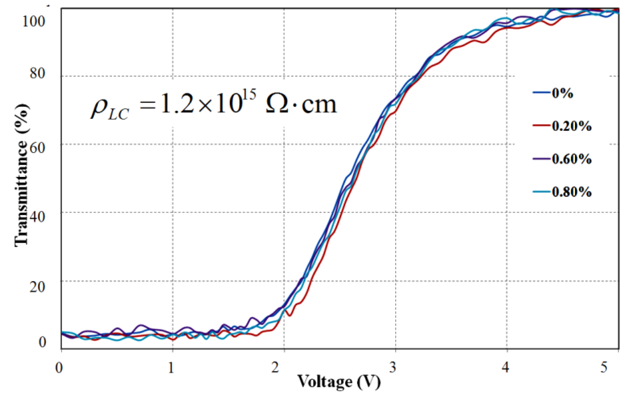
In this study, although the ITO particles did not affect the physical properties of the LC molecules at a low voltage below 5 V, the nano-ITO can still provide breakdown paths for host LC molecules under attack of an ESD arc. An interesting subject to explore is the role ITO plays in the LC. We attempt here to propose a model to explain the results of our measurements.

4.1. Model for ITO in LC under High Electric Field Intensity

Regarding the fast disappearance of the residual images for the doped cells, early studies on the breakdown of liquids containing particles [24,25,26] may offer us some indications on how ITO could assist in releasing the charges. It is known that the breakdown voltage of the insulating liquid can be significantly reduced if there is a small amount of contaminant or impurity. As reported by Kok and Corbey [24], “polarizable particles, ions, or colloidal contaminants of high dielectric constant, particularly conducting material”, may form conducting bridges on the attraction of non-uniform high electric fields. Similar findings were also obtained in other literature [25,26]. Therefore, it is fair to say that a contaminated insulating liquid would easily breakdown at high voltages.
Since ITO and LC molecules are transparent, they are not easily observed or discriminated even under a polarized microscope. Based on the findings in the mentioned references [24,25], we believe that the doped ITO particles would be driven by applied high fields and easily aggregate to create conductive bridges inside the LC layer.
Although it is not clear at present how the ITO particles conduct the accumulated charges in the doped samples and while the possible conducting paths were difficult to observe directly in this study, it is believed that the ITO particles acted as impurity particles to provide leaky paths under the attraction of the high electric field induced by the ESD.
At first glance, it seems unbelievable that the impurity particles could be driven to aggregate by the vertical electrical field exerted from the electrodes. As proposed in ref. [24] based on microscopic viewpoints, this indicates that the electric fields around defects or the colloidal particles are not uniform. Therefore, the electric field around these structural defects may not only be positioned vertically. Some horizontal fields could polarize the colloids and stress such randomly suspended particles to aggregate inside the colloid.
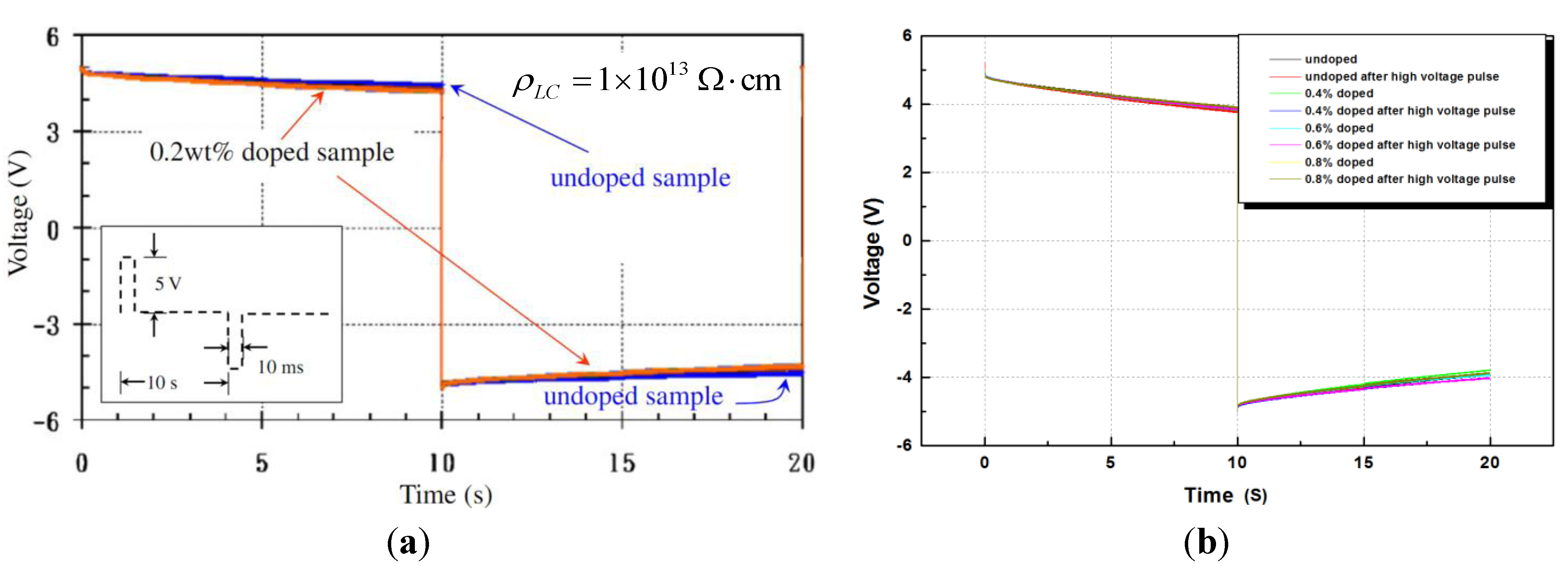
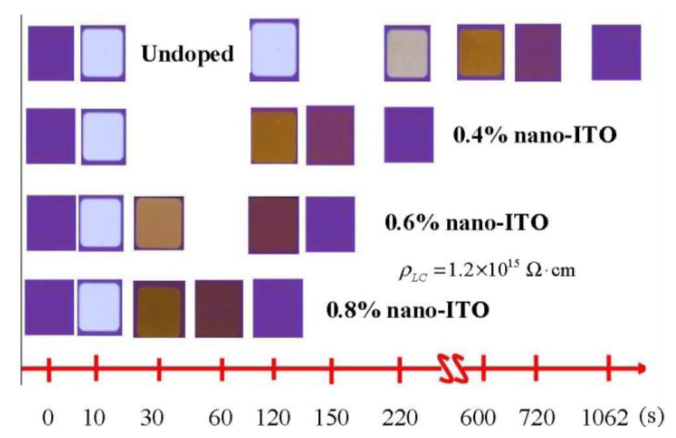
A scenario for the ITO particles to form conductive bridges and return back to their uniform distribution in the LC is described in the following. Based on the results from our V-T and VHR measurements, the dispersed ITO particles would not make the LC layer conducive prior to exerting the ESD pulse, also after the induced sticking image has vanished. According to the above explanation and our findings, it is reasonable that the ITO particles were polarized with the ESD stress and then aggregated quickly around a number of structural defects in the viscous LC due to a large horizontal field intensity. With the drifting of such polarized particles to flocculate locally, several conductive bridges in the insulating LC were then formed, however. The accumulated charges by ESD followed by being rapidly discharged. This means that these temporarily formed bridges provide several viable conducting paths to initiate local electrical breakdown in the LC cell. Thereby it is believed that an early breakdown phenomenon can quickly diminish the image sticking effect. Furthermore, such a mechanism may protect the LC from high voltage stresses. After the induced charges on the electrodes have disappeared, the electric field in the LC layer would drop down to a very low level, as the ITO particles began to diffuse from the bridges. Eventually these ITO particles would diffuse apart and re-distribute uniformly in the LC cells.
It should be noted that this proposed scenario was not physically confirmed by any direct observation or supported by any physical experiment. However, according to our experiments, the equivalent conductive paths would be beneficial for researchers to study the equivalent parameters dealing with the conductance in doped LC cells. In 
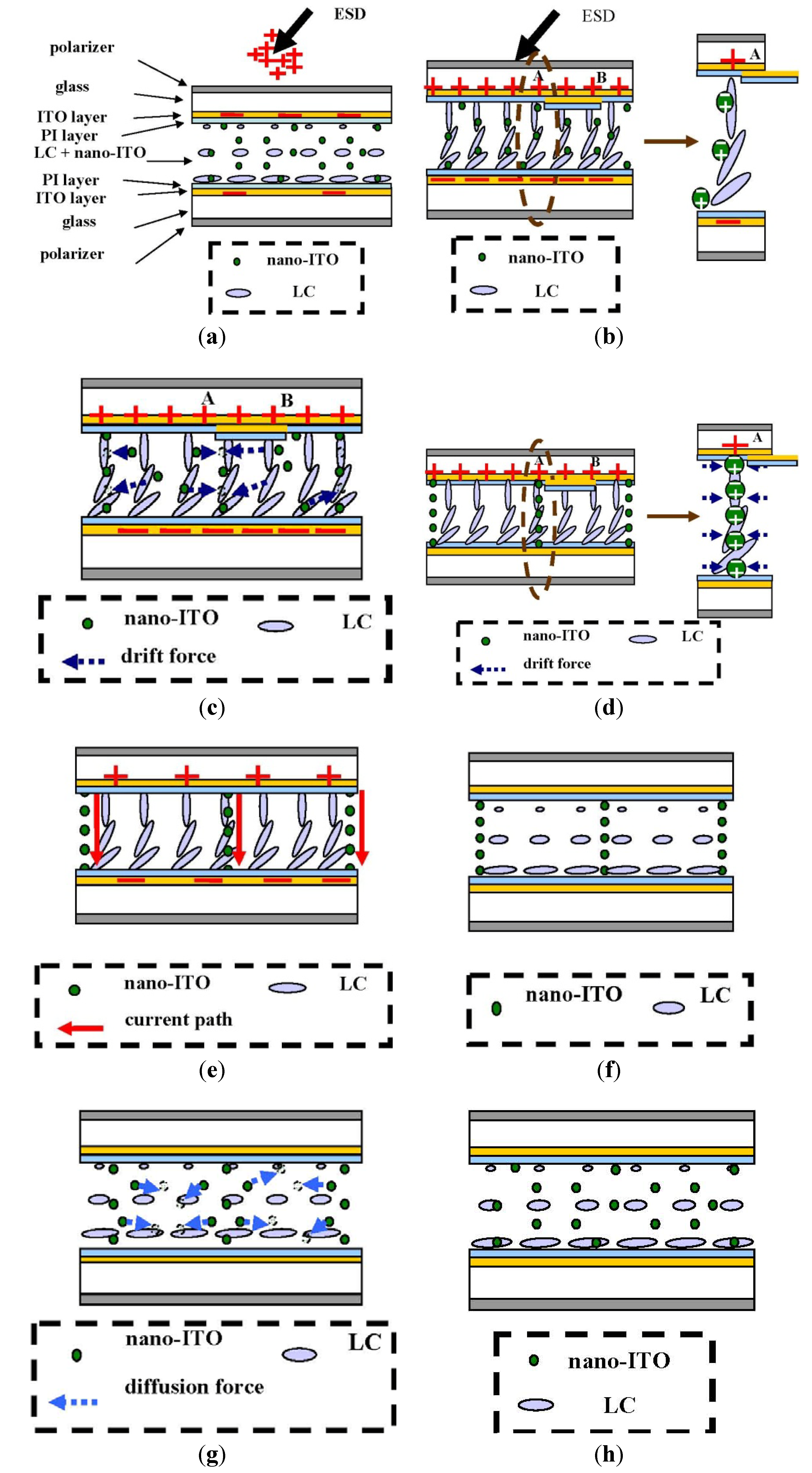
Figure 16 we provide a schematic expression to show the change of the accumulated charges and the reactions of the conductive ITO particles as well as the LC directors.
Figure 16. The hypothesized process for forming ITO bridges under high electric fields: (a) an HV gun approaches; (b) charges are induced by the HV gun; (c) non-uniform field intensity would cause ITO aggregates around the defected corners as at positions A and B in (b); (d) formation of ITO bridges after aggregation in (c); (e) the conductive bridges offer paths to release the induced charges in the electrodes; (f) after releasing the charges, the LC directors return to their TN state; (g) without the existence of a strong electrical field, the ITO particles begin to diffuse outwards from the bridges; (h) upon reaching the thermal equilibrium state, the ITO particles distribute randomly in the cell.
Crystals 03 00530 g016
Figure 16a illustrates an electric gun approaching a doped cell, in which the conductive particles are uniformly distributed in a TN LC cell. When the gun is charging the sample with the electric arc, as shown in Figure 16b, a fairly large amount of high voltage charge is induced on the electrodes and the LC directors would then be drawn up, which immediately triggers the sticking of an image on the cell. At the exact moment, the suspended particles are polarized by the external electric field and are attracted around the structural defects as shown in the right inset of Figure 16b,c. Figure 16b illustrates a particular situation, say at designated locations A and B, so they experience the non-uniformity of electric field from the microscopic viewpoint. These surface-charged particles around these designated locations, attract one another easily by the Coulomb forces between them and are accelerated in the direction traverse to the macroscopic electric field established by the high voltage charges at the electrodes, shown in Figure 16c. More complex aggregation may accelerate the formation of bridges at high voltage. As indicated in 
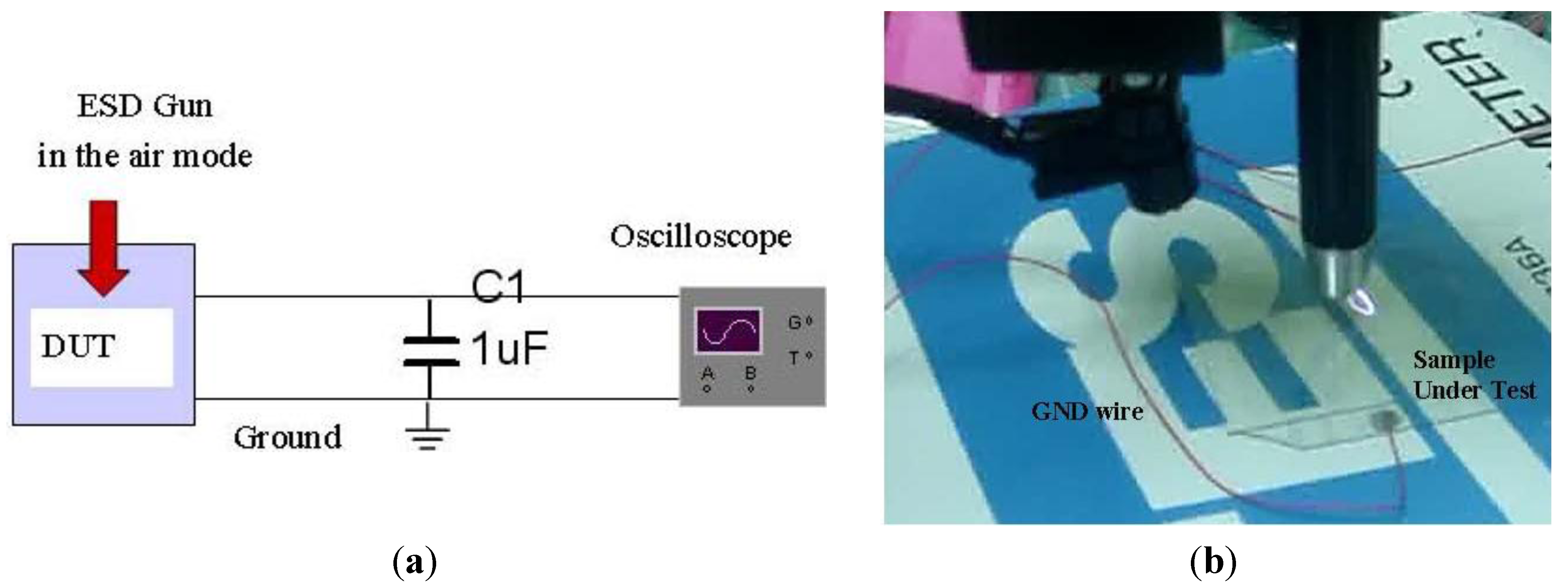
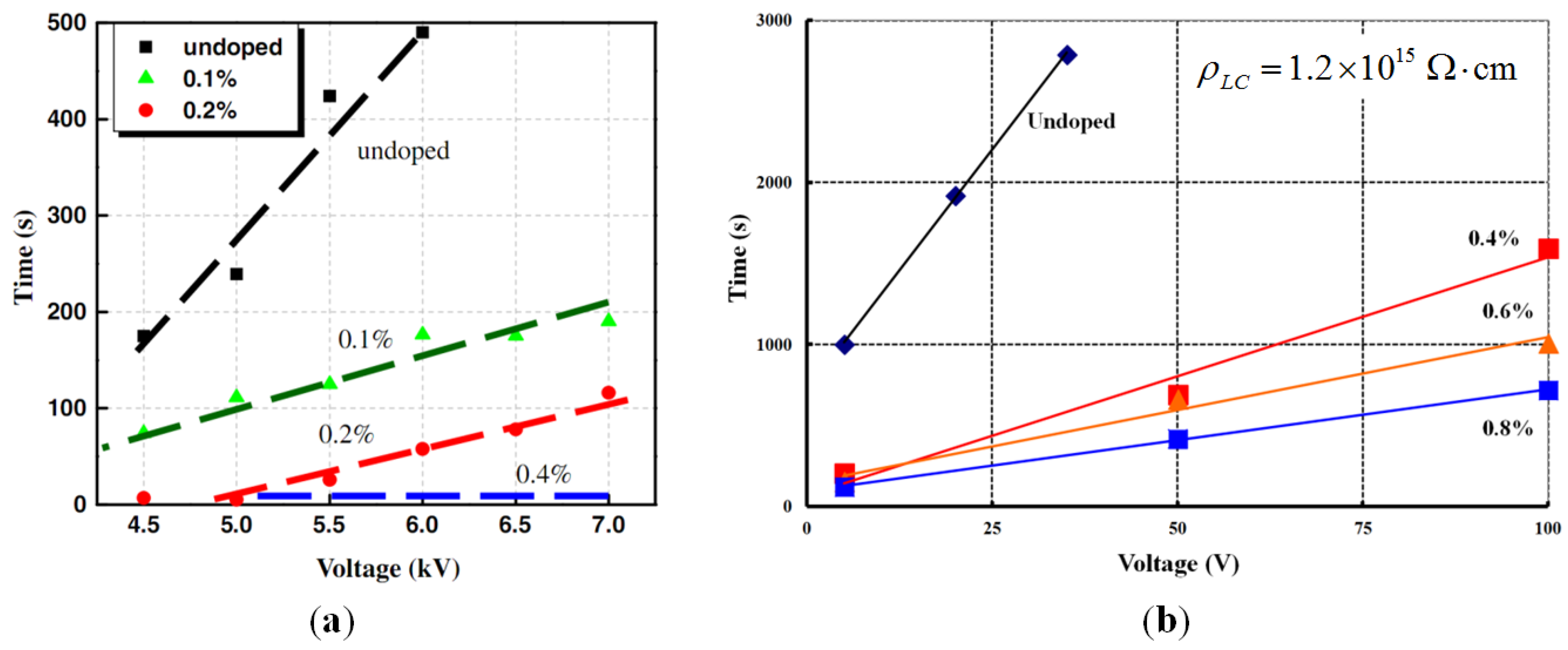
Figure 13, the estimated E-filed intensity in the undoped sample from the peak voltage reaches 200 V/cm. In fact, the actual E-field intensity should be much higher than this value due to the function of the auxiliary capacitor C1 in Figure 5a. Although the liquid crystal is a viscous fluid, it is believed that ITO nanoparticles have a higher mobility than their ITO agglomerates of a larger size. Subsequently these polarized particles can aggregate to form instantly a number of conducting bridges, as shown in Figure 16d, to then form several conducting paths to initiate the electrical breakdown, as shown in Figure 16e, for a rapid release of the accumulated charges between the electrodes. At this point, it does not matter if the electric gun is still discharging or is removed. The results shown in Figure 13 reveal that the formation of conducting bridges was instant and such bridges quickly released the induced charges in the doped samples during the ESD stress. Without the existence of the ITO bridges above-mentioned, the charge release would become a very slow process as in the cases of the undoped samples. Figure 16f represents the state of the LC directors after the electric gun has been removed and the induced charges have been totally released. In this case, the LC directors relax back to their initial TN states. Once the charges are removed, there is no strong horizontal electric field to support the bridges inside the LC. The conductive particles naturally diffuse outwards, as shown in Figure 16g, and distribute uniformly under the condition of thermal equilibrium, Figure 16h. With a current proposed model, it can be understood that the sticking images would be removed faster in a doped cell with a higher concentration of conductive particles. The proposed model is consistent with our findings. Notably, since the stuck images have been removed by releasing the charges, the extra time needed for the relaxation of the ITO bridges would not affect the images on the LC cells.
Based on our proposed model, some equivalent properties are investigated in the following.

4.2. Model for Estimating Densities of Conductive Bridges

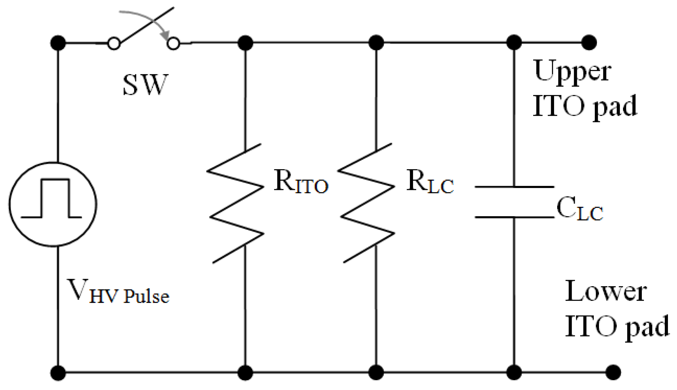
Based on the above concept, the equivalent circuit to explain the relaxation process of the LC samples can be simplified from that in Figure 7b and represented in Figure 17. In this equivalent circuit, CLC and RLC represent the electric properties of the LC. The effect of the PI layer can be excluded by considering only the effective voltage exerted on the LC layer. For the doped samples, RITO represents the equivalent resistance of the conductive ITO bridges that are formed by the electric field during the attacks of the high voltage pulses. Therefore, RITO was infinite for the undoped samples.
According to Figure 17, let us map the physical mechanisms for charging the LC by a high voltage pulse and for releasing the charges in the LC layer by the circuit with SW on. After applying a high voltage pulse, switch SW is open to isolate the LC sample from the pulse source. In this condition, CLC stores the high voltage charges. These charges will then be released by the parallel RC circuit in the exponential form as below:
Crystals 03 00530 i001
where Rtotal is the total resistance of the two parallel resistances, i.e., RITO//RLC. By extracting the time constant of relaxation, i.e., τr = Rtotal × CLC, the value of RITO can be determined.
Figure 17. The equivalent circuit for the sample in the high-voltage measurement.
Crystals 03 00530 g017
According to the physical parameters, the capacitance of the LC is obtained by
Crystals 03 00530 i002
where A is the area of the LC cell, d is its cell thickness, and εr is its relative dielectric constant. In this study, the LC samples we employed had the same parameters, i.e., A = 1.0 × 1.0 cm2, d = 4 μm, and εr = 5.9. With these parameters, the capacitance, CLC, used for all the LC samples in this study was 1.306 nF.
As for the value of RLC, the original resistance of the LC can be obtained from the undoped samples. By measuring directly on an undoped LC sample with a DC voltage, the obtained resistance, RLC, was 7.76 × 10¹¹ Ω.
This value can also be estimated from its geometric and material parameters, i.e.,
Crystals 03 00530 i003
where ρLC is the resistivity of the LC. As mentioned in the preparation of our samples, the nominal resistivity of the LC material was 1.2 × 10¹⁵ Ω∙cm. With the dimensions that A = 1.0×1.0 cm2 and d = 4 μm, the estimated resistance of our undoped samples was 4.8 × 10¹¹ Ω. The estimated and the measured values were very close. From this study, we chose the measured value for later investigations.

4.3. Resistivity of Conductive Bridges

With the concept as described for Equations (1)–(3) in the previous section, Table 2 lists the extracted electrical parameters for the results in Figure 15b. In addition, 
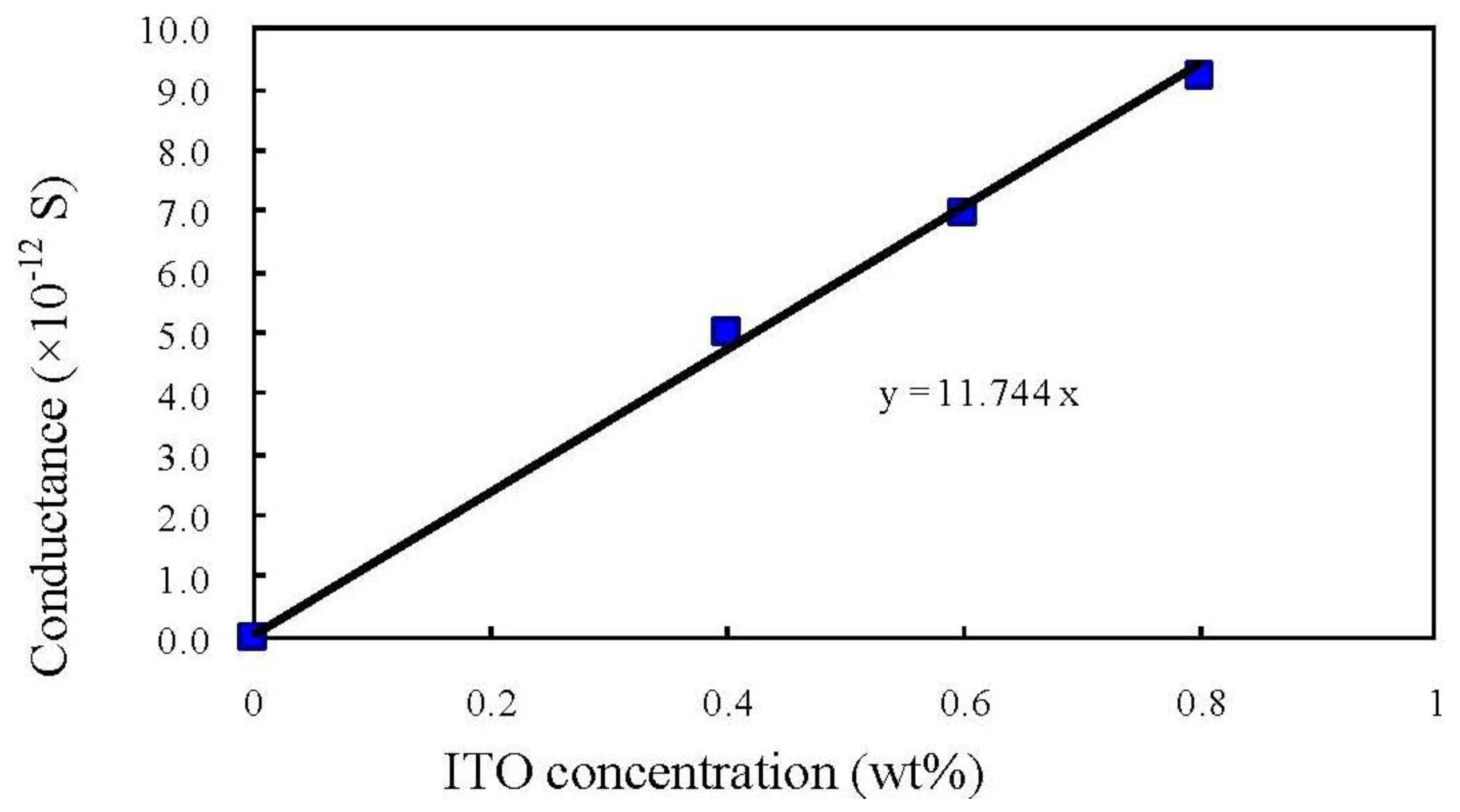
Figure 18 shows the relation between the intended ITO concentration and the extracted ITO resistance, RITO.
As seen in Table 2, the time constant, τr, was obtained from Equation (1) by assuming V0 = 5 V for Figure 12. The total resistance, Rtotal, was then derived by τr/CLC. Therefore, the ITO resistance, RITO, can be obtained by excluding RLC from Rtotal. In this study, CLC and RLC were presumed the same for all the calculations. It is interesting to note in Table 1 that the estimated RLC derived from the obtained time constant for the undoped sample is 7.73 × 10¹¹ Ω, which was very close to that obtained from the DC measurement as described in Section 4.2. As a consequence, we believe that this time-constant method is precise enough to estimate RITO.
Table 2. Extracted electrical parameters.
ITO concentrationτr (s)Rtotal (Ω)RLC (Ω)RITO (Ω)
0.00 wt %1.01 × 1037.73 × 10117.76 × 1011 ***
0.40 wt %2.06 × 1021.58 × 10117.76 × 1011 *1.98 × 1011
0.60 wt %1.58 × 1021.21 × 10117.76 × 1011 *1.43 × 1011
0.80 wt %1.24 × 1029.50 × 10117.76 × 1011 *1.08 × 1011
Notes: * presumed by DC measurements, ** presumed value.
According to the results listed in Table 2, one can also find that the trends of Rtotal and RITO are reasonable. That is, the sample with a higher concentration of ITO gives both lower Rtotal and RITO. In Figure 18, it can also be seen that the inverse of RITO is linearly proportional to the ITO concentration. This fact supports our proposed model that more ITO particles would form more conductive bridges between the upper and lower electrical contacts under a high electric field intensity [19,20].
Based on the above findings, it was attempted to estimate the density of ITO bridges. By assuming that the resistances of these conductive bridges were the same as RBR, the conductive bridges can be regarded simply as several conductive chains as depicted in Figure 16 which would exhibit total resistance, RITO, by the following relation, i.e.,
Crystals 03 00530 i004
where NBR is the number of the bridges or chains per unit area in the LC cell. If the value of RBR is known, the surface density NBR can be evaluated from Equation (4). However, from the microscopic viewpoint, the ITO particles may not be bound tightly with each other in the conductive chains as imagined in 
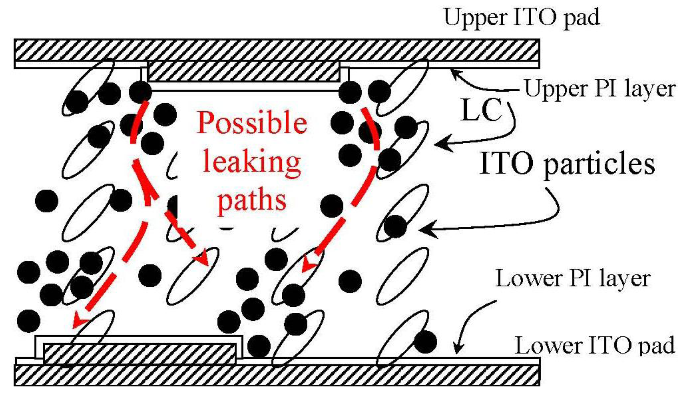
Figure 16. A more realistic picture of the conductive ITO bridges is presented in Figure 19. With the existence of the structural defects, ITO particles under high electric field intensity may aggregate around such defects and form possible leaky paths. The ITO particles are still loosely bonded around the paths. Therefore, the spacing between the ITO particles in the conductive chain is unknown. RBR cannot be determined directly from its geometry. For the present study, RBR and NBR cannot be definitely determined independently.
Figure 18. Relation of ITO concentration vs. the inverse of the extracted ITO resistance (1/RITO).
Crystals 03 00530 g018
Figure 19. Pictorial presentation of ITO conductive paths in LC under high electric fields.
Crystals 03 00530 g019
Even with lack of clarity in determining RBR and NBR, the range of RBR can still be estimated. Since NBR > 1, it can be certain that in Equation (4) RITO is the lower limit for RBR. Therefore, the minimal RBR can be replaced by RITO. Considering the structure as represented in Figure 19, RBR can be expressed as
Crystals 03 00530 i005
where ρBR is the resistivity of the ITO bridge; ABR is the cross sectional area of the bridge; and d is equivalent to the layer thickness of the LC in the samples. In this study, the average diameter of ITO particles was 30 nm. ABR may be estimated as 7.07 × 10⁻¹² cm2 and d is 4 μm for our samples. If we take the value of RITO forh the lowest ITO concentration in this study as the lower limit of RBR, then RBRmin =1.98 × 10¹¹ Ω from Table 2. With Equation (5) with the above parameters, the lower limit of ρBR is determined as 3.50 × 10³ Ω∙cm.
Let us now compare the obtained resistivity of the ITO bridges and that of the original ITO powders by the four-point probe method in Section 2.2. The resistivity of the original ITO powders was around 100 Ω∙cm. Clearly the minimal ρBR is higher than the original value by 30 times. Our finding indicates that the ITO particles in the conductive bridges are loosely bonded to another one. Since the relative movement of ITO particles in the viscous LC is expected to be not too high, the pictorial model of loosely bonded ITO chains in the LC described herein is acceptable and reasonable in our study.

5. Conclusions

In this paper, the effects of ITO in protecting LCs against ESD are described according to results of our studies. We successfully designed several characterization setups for investigation. An interesting effect of the nano-ITO on the breakdown property of the high resistance LC was found.
According to our experiments, it was found that nano-ITO can effectively protect LC cells from attacks of ESD. As a consequence, the problem of the induced image sticking on the cell is profoundly resolved. In this study, a higher concentration of ITO in the doped samples rendered a lower amount of ESD-induced charge. Furthermore, even with the presence of the conductive material, fundamental properties such as optical transmittance, VHR and electrical leakage at low voltage are unaffected. The possible reason may be attributed to that fact that the nano-ITO particles did not react with the LC. However, these ITO particles may themselves offer leaky paths under conditions when a very high voltage is exerted. Based on the short residual time of the ESD-image and the unaffected fundamental properties of the high resistance LC, this study provides new insight for display engineers in designing and fabricating novel LC devices.
According to the results, by measuring the relaxation time of the sticking images induced by the high-voltage pulses, a hypothetical model for ITO in a LC was used to investigate the electrical properties of the doped LC cells. Based on the relation between RITO and ITO concentration in our study, the existence of conductive ITO bridges is consistent with our experiments. In addition, the lower limit of the real resistivity of the ITO bridges was estimated as 3.50 × 10³ Ω∙cm which was 30 times higher than that of the ITO powders. This finding indicates that the nature of the equivalent ITO bridges created by the high electric field intensity is a loosely bonded structure.

Acknowledgments

The authors gratefully acknowledge the supports from Wintek Corporation and National Science Council (NSC), Taiwan, under the contract Nos. NSC 101-2221-E-035-065- and NSC 95-2221-E-035-108-MY2.

Conflicts of Interest

The authors declare no conflict of interest.

References

  1. Thisayukta, J.; Shiraki, H.; Sakai, Y.; Masumi, T.; Kundu, S.; Shiraishi, Y.; Toshima, N.; Kobayashi, S. Dielectric Properties of Frequency Modulation Twisted Nematic LCDs Doped with Silver Nanoparticles. Jpn. J. Appl. Phys. 2004, 43, 5430–5434. [Google Scholar] [CrossRef]
  2. Yoshikawa, S.; Maeda, K.; Shiraishi, Y.; Xu, J.; Shiraki, H.; Toshima, N.; Kobayashi, S. Frequency Modulation Response of a Tunable Birefringent Mode Nematic Liquid Crystal Electrooptic Device Fabricated by Doping Nanoparticles of Pd Covered with Liquid-Crystal Molecules. Jpn. J. Appl. Phys. 2002, 41, L1315–L1317. [Google Scholar] [CrossRef]
  3. Huang, C.-Y.; Pan, H.-C.; Hsieh, C.-T. Electrooptical Properties of Carbon-Nanotube-Doped Twisted Nematic Liquid Crystal Cell. Jpn. J. Appl. Phys. 2006, 45, 6392–6394. [Google Scholar]
  4. Jeong, S.-J.; Suresh, K.; Jeong, K.-U.; Srivastava, A.K.; Lee, S.-H.; Jeong, S.-H.; Lee, Y.-H.; Lu, R.; Wu, S.-T. Unusual double four-lobe textures generated by the motion of carbon nanotubes in a nematic liquid crystal. Opt. Express 2007, 15, 11698–11705. [Google Scholar] [CrossRef]
  5. Ouskova, E.; Buchnev, O.; Reshetnyak, V.; Reznikov, Y.; Kresse, H. Dielectric relaxation spectroscopy of a nematic liquid crystal doped with ferroelectric Sn2P2S6 nanoparticles. Liq. Cryst. 2003, 30, 1235–1239. [Google Scholar] [CrossRef]
  6. Tseng, J.-C.; Hwu, J.-G. Effects of electrostatic discharge high-field current impulse on oxide breakdown. J. Appl. Phys. 2007, 101, 014103:1–014103:6. [Google Scholar]
  7. Golo, N.T.; van der Wal, S.; Kuper, F.G.; Mouthaan, T. Estimation of the impact of electrostatic discharge on density of states in hydrogenated amorphous silicon thin-film transistors. Appl. Phys. Lett. 2002, 80, 3337–3339. [Google Scholar] [CrossRef]
  8. Jiang, B.-R.; Liu, C.-Y.; Chen, C.-J.; Tseng, K.-S.; Chang, L.-H. Liquid Crystal Display and ESD Protection Circuit Thereof. U.S. Patent 7,375,724, 20 May 2008. [Google Scholar]
  9. Kusanagi, T. Liquid Crystal Display Having Electrostatic Discharge Damage Prevention. U.S. Patent 6,108,057, 22 August 2000. [Google Scholar]
  10. Sonoda, H.; Ohe, M.; Asuma, H.; Matsuyama, S. Liquid Crystal Display Device Having a Spacer. U.S. Patent 6,433,852, 13 August 2002. [Google Scholar]
  11. Lee, W.; Wang, C.-Y.; Shih, Y.-C. Effects of carbon nanosolids on the electro-optical properties of a twisted nematic liquid-crystal host. Appl. Phys. Lett. 2004, 85, 513–515. [Google Scholar]
  12. Baik, I.-S.; Jeon, S.Y.; Lee, S.H.; Park, K.A.; Jeong, S.H.; An, K.H.; Lee, Y.H. Electrical-field effect on carbon nanotubes in a twisted nematic liquid crystal cell. Appl. Phys. Lett. 2005, 87, 263110:1–263110:3. [Google Scholar]
  13. Shah, H.J.; Fontecchio, A.K.; Mattia, D.; Gogotsi, Y. Field controlled nematic-to-isotropic phase transition in liquid crystal-carbon nanotube composties. J. Appl. Phys. 2008, 103, 064314:1–064314:5. [Google Scholar]
  14. Chen, P.-S.; Huang, C.-C.; Liu, Y.-W.; Chao, C.-Y. Effect of insulating-nanoparticles addition on ion current and voltage-holding ratio in nematic liquid crystal cells. Appl. Phys. Lett. 2007, 90, 211111:1–211111:3. [Google Scholar]
  15. Lin, T.-J.; Chen, C.-C.; Cheng, S.; Chen, Y.-F. Liquid crystal cells with built-in CdSe nanotubes for chromogenic smart emission devices. Opt. Express 2008, 16, 671–678. [Google Scholar] [CrossRef]
  16. Kuo, C.-W.; Jeng, S.-C.; Wang, H.-L.; Liao, C.-C. Application of nanoparticle-induced vertical alignment in hybrid-aligned nematic liquid crystal cell. Appl. Phys. Lett. 2007, 91, 141103:1–141103:3. [Google Scholar]
  17. Hwang, S.-J.; Jeng, S.-C.; Yang, C.-Y.; Kuo, C.-W.; Liao, C.-C. Characteristics of nanoparticle-doped homeotropic liquid crystal devices. J. Phys. Appl. Phys. 2009, 42, 025102:1–025102:6. [Google Scholar]
  18. Buchnev, O.; Dyadyusha, A.; Kaczmarek, M.; Reshetnyak, V.; Reznikov, Y. Enhanced two-beam coupling in colloids of ferroelectric nanoparticles in liquid crystals. J. Opt. Soc. Am. 2007, 24, 1512–1516. [Google Scholar] [CrossRef]
  19. Liang, B.-J.; Liu, D.-G.; Shie, W.-Y.; Huang, S.-R. Effects of Nanoscaled Tin-Doped Indium Oxide on the Image Sticking Property of Liquid Crystal Cells. Jpn. J. Appl. Phys. 2010, 49, 025004:1–025004:6. [Google Scholar]
  20. Liang, B.-J.; Liu, D.-G.; Chang, C.-Y.; Shie, W.-Y. Effects of Concentration of Nanoscale Tin-Doped Indium Oxide on Electrical Breakdown of High-Resistance Liquid Crystal. Jpn. J. Appl. Phys. 2011, 50, 055002:1–055002:5. [Google Scholar]
  21. Gurev, H.S.; Bicking, K. Indium tin oxide (ITO) coating of curved polymer substrates. J. Proc. SPIE 1994, 2262, 246–255. [Google Scholar] [CrossRef]
  22. Josell, D.; Brongersma, S.H.; Tőkei, Z. Size-Dependent Resistivity in Nanoscale Interconnects. Annu. Rev. Mater. Res. 2009, 39, 231–254. [Google Scholar] [CrossRef]
  23. Chen, W.-Y.; Ker, M.-D.; Huang, Y.-J. Investigation on the Validity of Holding Voltage in High-Voltage Devices Measured by Transmission-Line-Pulsing (TLP). IEEE Electron. Dev. Lett. 2008, 29, 762–764. [Google Scholar] [CrossRef]
  24. Kok, J.A.; Corbey, M.M.G. Dipoles and electric breakdown. Appl. Sci. Res. Sect. 1957, 6, 449–455. [Google Scholar]
  25. Tortai, J.H.; Bonifaci, N.; Denat, A. Insulating properties of some liquids after an electrical arc. IEEE Trans. Dielectr. Electr. Insul. 2002, 9, 3–9. [Google Scholar] [CrossRef]
  26. Kuffel, E.; Abdullah, M. High Voltage Engineering; Pergamon Press Ltd.: New York, NY, USA, 1970. [Google Scholar]

