Article

Controlled Deposition of Tin Oxide and Silver Nanoparticles Using Microcontact Printing

by
Joo C. Chan
1,
Nicole Hannah-Moore
2 and
Shankar B. Rananavare
2,*
1
Intel D1C Lithography Engineering, Intel Corporation, Ronler Acres, Hillsboro, OR 97124, USA
2
Department of Chemistry, Portland State University, Portland, OR 97207, USA
*
Author to whom correspondence should be addressed.
Crystals 2015, 5(1), 116-142; https://doi.org/10.3390/cryst5010116
Submission received: 2 October 2014 / Accepted: 4 February 2015 / Published: 13 February 2015
(This article belongs to the Special Issue Nanostructured Oxide Crystals)

Abstract

:
This report describes extensive studies of deposition processes involving tin oxide (SnOx) nanoparticles on smooth glass surfaces. We demonstrate the use of smooth films of these nanoparticles as a platform for spatially-selective electroless deposition of silver by soft lithographic stamping. The edge and height roughness of the depositing metallic films are 100 nm and 20 nm, respectively, controlled by the intrinsic size of the nanoparticles. Mixtures of alcohols as capping agents provide further control over the size and shape of nanoparticles clusters. The distribution of cluster heights obtained by atomic force microscopy (AFM) is modeled through a modified heterogeneous nucleation theory as well as Oswald ripening. The thermodynamic modeling of the wetting properties of nanoparticles aggregates provides insight into their mechanism of formation and how their properties might be further exploited in wide-ranging applications.

Graphical Abstract

1. Introduction

Electroless metal deposition (EMD) on dielectric substrates using a surface functionalizing catalyst has been widely utilized by industrial manufacturers because of its energy- and cost-efficiency. A classic example of this process is the deposition of silver on glass [1,2] in production of mirrors [3,4]. Typically the EMD process entails sensitizing a substrate with a reducing agent followed by metal deposition in a solution containing metal ions and an additional reducing agent. EMD on dielectric substrates lends itself to patterning of metals, first achieved by photo-selective metal deposition [5,6,7,8] (PSMD) using UV light exposure and chemical solutions. PSMD has been employed to deposit copper, silver, and gold using palladium and tin catalysts. There has been a renewed interest in EMD of copper [9] on surfaces coated with self-assembled monolayers (SAMs) of surfactants bearing catalysts. Such patterned metal films may offer a low cost alternative to fabricating interconnects in modern semiconductor devices, replacing contemporary evaporative (e.g., aluminum) or electrochemical (e.g., copper) methods of deposition. Sub-micron scale patterning capability of EMD needs to be demonstrated to compete with the current interconnect patterning [10,11,12,13,14] using electrochemical deposition, the so-called dual damascene process [15,16].
Flame aerosol deposition (FAD) is another promising technique for electroless deposition of nanoparticles on substrates [17]. Here a flame of nanoparticle-laden aerosol is directed at the substrates through a shadow mask providing patterning of deposited material on the scale of microns. The method is valuable for fabricating sensors especially those based on metals and oxides. The method leads to films of high porosity that can be compacted by annealing. The thermal annealing improves film-substrate adhesion leading to better processibility in wafer scale manufacturing.
Recently techniques of soft lithography [18,19,20,21] have been employed to craft sub-micron size patterns. Of these techniques, micro-contact printing using polymer (typically poly(dimethylsiloxane), PDMS) stamps has several attractive features. First, the method is inexpensive while still permitting high-resolution printing (≈20 nm). Second, once a high-resolution master is created, printing does not suffer from the resolution limitations of optical lithography. Third, by using organic surfactants, especially thiol-based surfactants [22,23], as ink to produce SAMs, the method can fabricate defined metal patterns [9] in EMD. The technique has the limitation that it leaves a surfactant monolayer underneath the metal film, which may lead to delamination of the film during heating to the elevated temperatures normally used in processing wafers. Other approaches have printed SAMs of thiols as a resist for patterning metal films. Recently transistors and flexible displays were fabricated using this latter technique [24,25]. Rogers et al. [24] note that the linewidth roughness of electrodeposited source and drain silver contacts may influence the carrier mobility. These studies illustrate the viability of soft lithographic approaches for the fabrication of electronic devices.
This paper examines several underlying surface chemical and physical phenomena involved in EMD. We show how the patterned surface-resident sensitizing catalyst, a nonstoichiometric oxide of tin, influences the structure and roughness of deposited metal films. The studies of electroless silver deposition presented here reveal that SnOx nanoparticles, used to catalyze Ag deposition, can themselves form films that resemble self-assembled monolayers (SAMs) on glass substrates [26]. We exploit this feature of SnOx nanoparticle films to provide controlled deposition of silver films on glass. Suspension of SnOx nanoparticle sensitizer is used as ink for the PDMS stamping of the desired patterns. Our approach avoids the use of surfactant based SAMs at any stage of metal deposition and patterning.
The following is a brief outline of the paper. We begin with results from a set of experiments using microcontact printing of the sensitized SnOx nanoparticles, illustrating their potential as catalysts for spatially-selective deposition of silver. Morphology of the SnOx film is shown to affect the vertical as well as the lateral roughness of the overlying silver films. Therefore, we conducted studies of the growth of SnOx on glass surfaces as functions of time and SnCl2 concentration in the sensitizing solution followed by the influence of capping agents in altering the shape and the size (i.e., the morphology) of catalyst deposition. We use atomic force microscopic (AFM) technique to determine and quantify the morphology of SnOx aggregates in terms of their contact angle and the radius of curvature. We describe simple molecular and nucleation models that provide an intuitive basis for understanding the observed distribution functions of height for the surface deposited clusters. This modeling yields surface energies of the clusters and electrostatic repulsive forces amongst them.

2. Results and Discussion

2.1. Results

A sensitizer used in these studies employs freshly prepared aqueous solutions of SnCl2. The microstructure of the resulting colloidal solution is complex and affects the quality and the resolution of patterned EMD. Dissolved oxygen in such solutions partially oxidizes the Sn2+ producing its hydrated oxides that ripen by the sol-gel process to form SnOx (x < 2) nanoparticles. Unfortunately, the formation of complex oxychlorides, oxides of mixed Sn oxidation states, and the influence of dissolved oxygen on its colloidal structure [5,7,8] prevent monitoring of the growth, or even determination of the chemical composition of the SnOx particles in solution. It is also known [27,28,29] that the size of SnOx nanoparticles in the aqueous solutions depends strongly on pH [30]. The catalytic activity of such solution decreases with time presumably due to oxidation of Sn2+ to Sn4+, which is unable to reduce and deposit Ag+ ions on a sensitized surface.

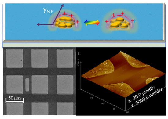
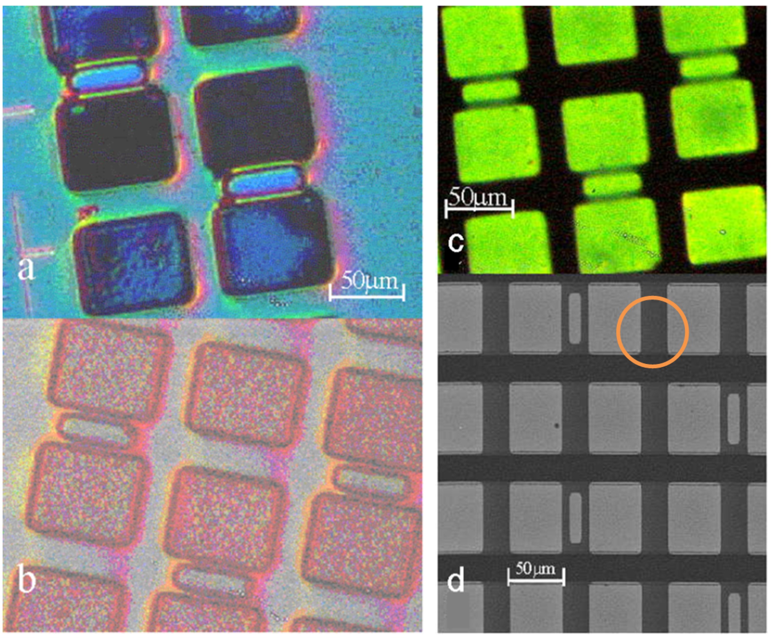
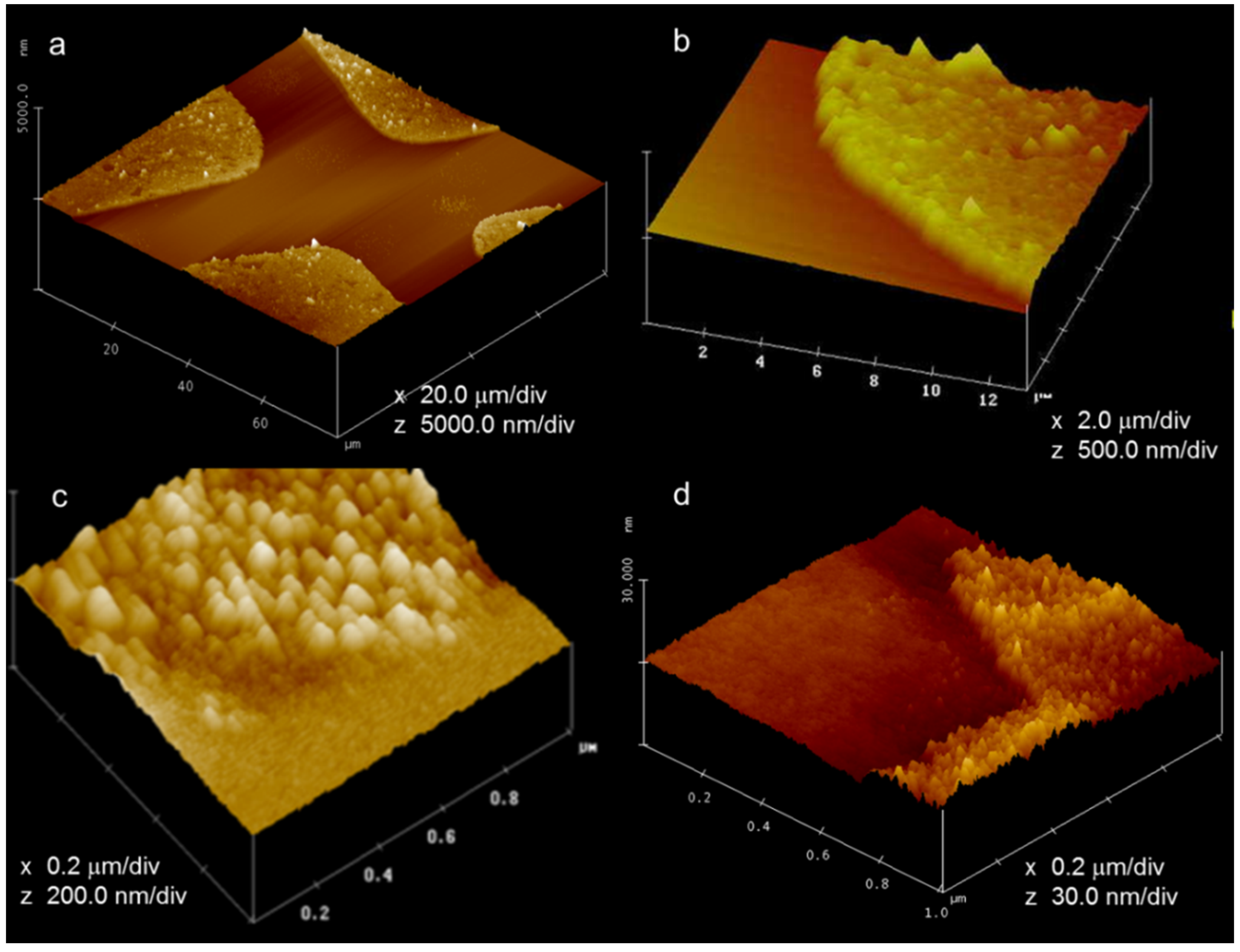
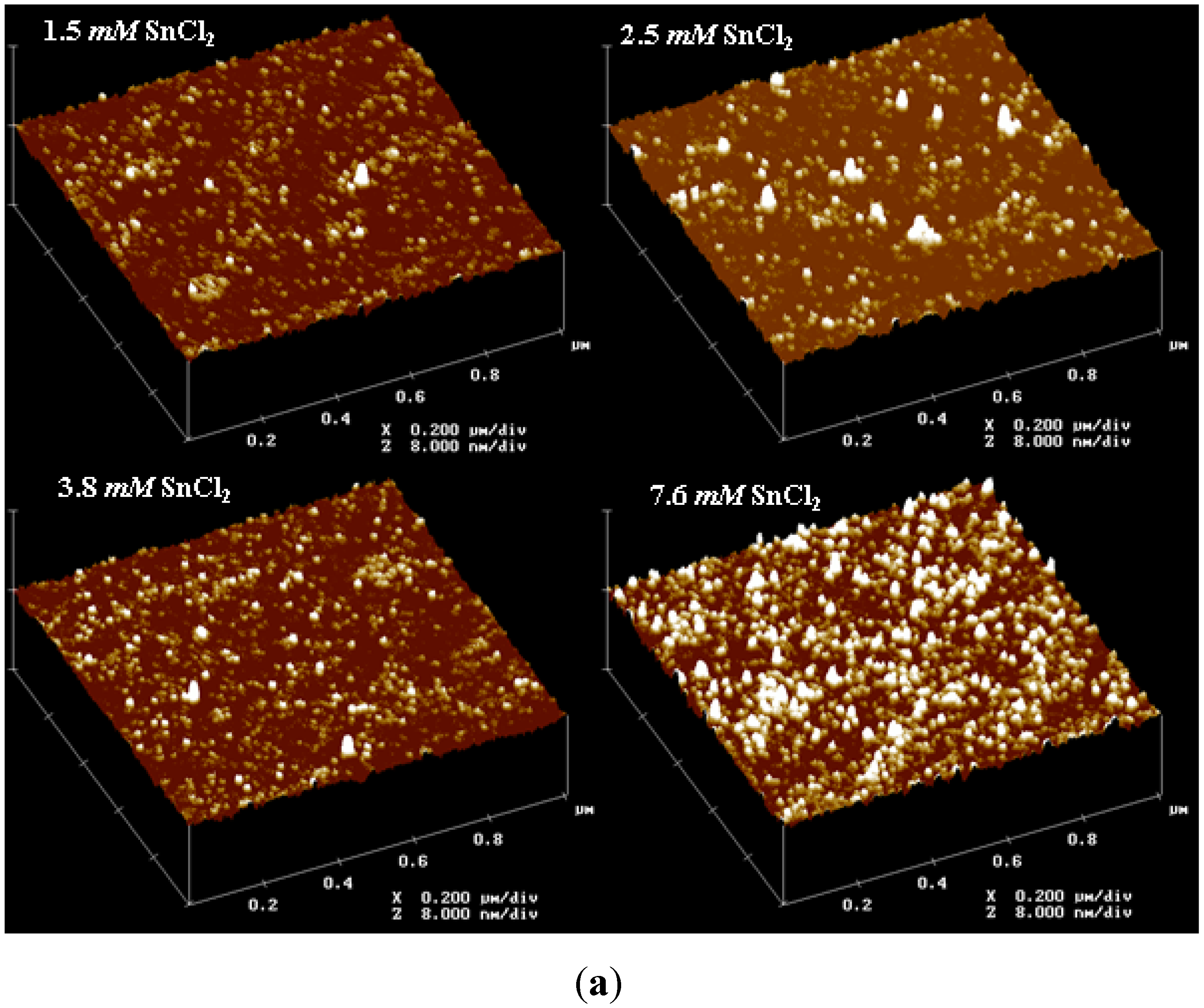
2.1.1. Controlled Deposition of Sensitizing SnOx Nanoparticles

The scheme for producing controlled deposition of silver on glass surface is presented in Figure 1.
Figure 1. Schematic of the process flow for fabrication of poly(dimethylsiloxane) (PDMS) stamp and controlled deposition of SnOx catalyst, followed by electroless deposition of silver.
Crystals 05 00116 g001
The process involves creating patterns in the PDMS stamp by curing it over a patterned master, followed by inking and printing the sensitizer. The details are presented in the experimental Section 3.
The key factors in controlling deposition are the time between “inking” the PDMS stamp with SnCl2/SnOx suspension and printing on the glass surface. If the interval is too short then the tendency to smear is high. Spotty deposition occurs if the interval is too long. The optimal time for drying the ink on the PDMS surface is about 1 min. Several images obtained by optical and scanning electron microscopy images taken during the various stages of the above scheme appear in Figure 2.
Figure 2. Optical and scanning electron microscopic (SEM) images of master, PDMS stamp and deposition patterns of SnOx and silver (a); Reflection microscopic image of a Cu integrated circuit (IC) chip used as a master for creating a patterned PDMS stamp (b); The corresponding image of the PDMS master stamp generated from (a), shown on an identical length scale (c); An optical image of the silver deposition pattern (deposited from 0.91 mM [Ag+] in silvering solution) created on a microscope coverslip using SnCl2 sensitizer (27 mM) and stamp shown in (b) and (d); The corresponding SEM image of the same silver pattern. The circle shows a region that was investigated using atomic force microscopy (AFM) (Figure 3).
Crystals 05 00116 g002
Micrographs of IC chip (Figure 2a), PDMS stamp (Figure 2b), and deposited silver (Figure 2c,d) show that controlled silver-deposition occurs only in the area where catalyst was printed.
AFM studies of the sample shown in Figure 2d were undertaken to probe higher resolution morphology of the deposited silver. The deposition is spatially well controlled over a wide range of scales from nano- to macroscopic, Figure 3. The microcontact printed films exhibit characteristic roughness in height (z direction) and in the lateral edges (x–y plane). Analyzing the height of the silver film revealed an average thickness of 130 nm with significant z-roughness (9 nm) caused by the particulate nature [9] of the film (Figure 3c). Here the z-roughness is defined as an arithmetic average of the absolute value of height deviation from the mean height of the film. Another metric of the film roughness is the z-range, which is defined as a difference between the maximum and minimum penetrable probe depth on the film surface. The size of silver nanoparticles [24,25] (diameter, D ≈ 30–40 nm) controls the roughness both in the x–y plane (3D ≈ 100 nm) and in the vertical (z). The z-range value of the silver film is about 30 nm needing significant improvement for submicron patterning.
Figure 3. AFM images of deposited silver and SnOx sensitizer (a); Stamped and developed pattern of silver particles at low magnification (b); Same pattern of silver at high magnification (c); Image of a deposited silver film near a corner of the pattern at higher magnification (d). Printed SnOx sensitizer at high magnification. The same concentrations of SnCl2 and silver are used here and Figure 2.
Crystals 05 00116 g003
We systematically investigated the factors affecting the silver film roughness. To probe how the underlying layer of SnOx sensitizer affects this roughness and resolution, we present an AFM image of stamped SnOx on a coverslip glass in Figure 3d.
The thickness of the SnOx layer is an order of magnitude lower than the silver film seen in Figure 3c. The maximum surface height of the film with respect to the underlying glass surface (Figure 3d) is 7 nm, comparable to the size of SnOx nanoparticles observed in other studies [7,8,27]. This implies that the stamped sensitizer film on glass is made up of roughly a monolayer of SnOx nanoparticles. Unfortunately the radius of the AFM tip (5–10 nm) prevents reliable measurements of the lateral size and packing of SnOx nanoparticles. Deconvolution of AFM patterns in this range of sizes requires assumption concerning the size and shape of the tip [31,32] and the shape of the particles. We estimate the worst-case z-range to be 3 × 7 nm = 21 nm. Thus, the edge-roughness and z-roughness in silvered and un-silvered (SnOx only) films is clearly affected by the size of the SnOx particles.

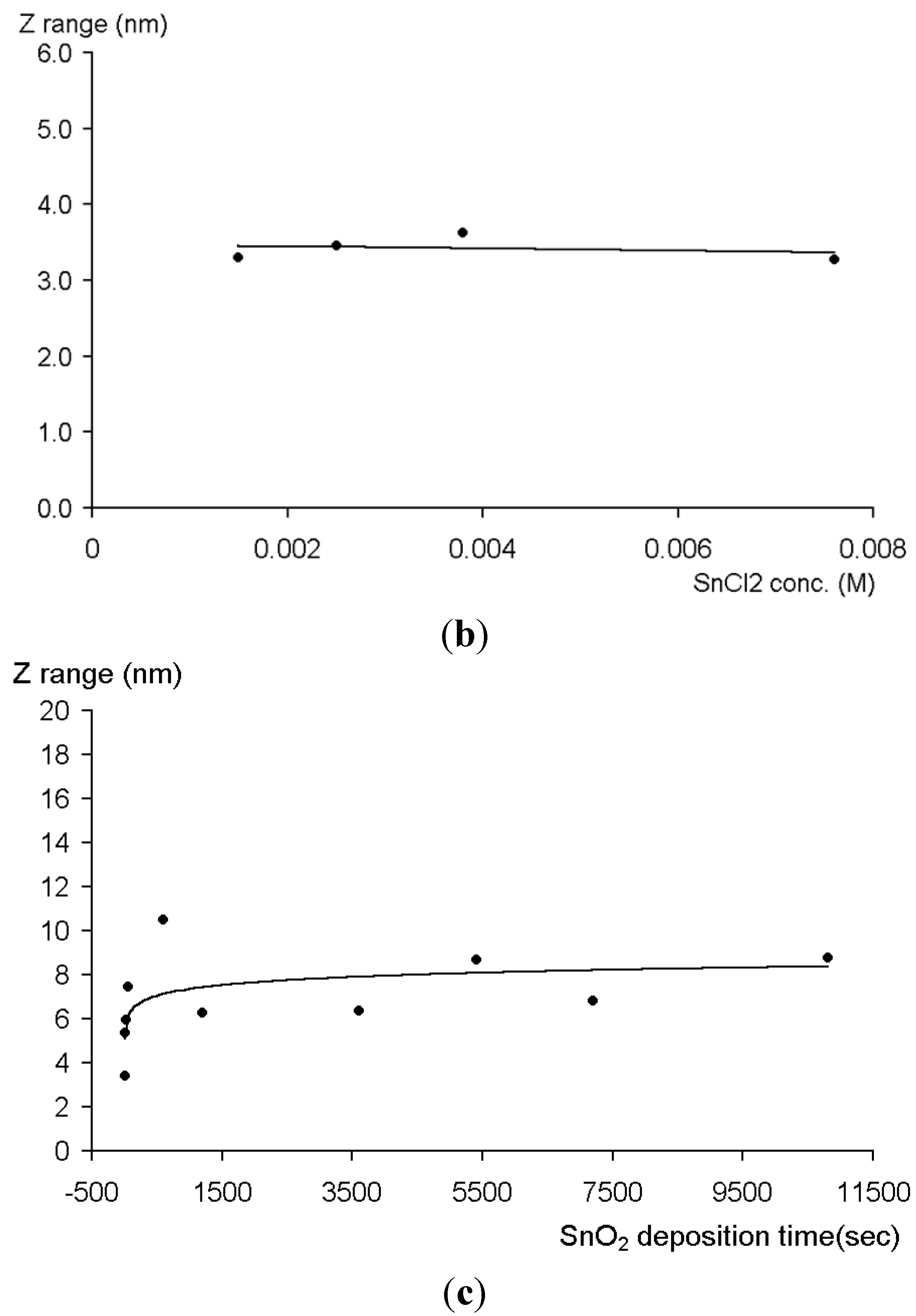
2.1.2. Unpatterned Deposition of Sensitizer from Solution on Planar Glass

The particulate film in Figure 3d is dense and AFM cannot laterally resolve the nanoparticles in the deposited SnOx. To produce films with lower densities where particles are separated from each other we employed diluted sensitizer solutions. The corresponding AFM studies of deposition on microscope cover slips appear in Figure 4a. To study growth in z-direction, AFM studies as a function of deposition-time were conducted (Supplementary Figure S1). The measured z-ranges for these sets of samples are shown in Figure 4b,c.
Figure 4a displays well-separated nanoparticles on a glass cover-slip surface. Their packing density increases with sensitizer concentration. Above 0.0076 M concentration they approach a closed-packed assembly. AFM here provides the height of the particles unaffected by the tip resolution because the particles are separated by a distance greater than the tip diameter. The z-range data in Figure 4b gives the size of the SnOx nanoparticles of 4 ± 1 nm independent of the sensitizer concentration. At higher concentration, as well as during longer deposition times up to four hours, the surface is densely packed with little roughness. The z-range presented in Figure 4c evolves from about 4 ± 1 nm to 7 ± 2 nm within first few minutes and remains constant thereafter. The asymptotic value is roughly twice the size of particles estimated from Figure 4b. The approximate size of SnOx nanoparticles (4 ± 1 nm) is twice the height (7 ± 2 nm) of stamped SnOx film shown in Figure 3d, implying that a monolayer/bilayer of SnOx nanoparticles is transferred during the stamping process. Thus, films containing SnOx nanoparticles behave like SAMs of surfactants commonly used in soft lithographic stamping [20].
Figure 4. Growth of the z-roughness as a function of the sensitizer concentration and the deposition time (a); AFM images of deposited SnOx at different concentration of sensitizer. Horizontal and vertical scales are 200 nm/div and 8 nm/div respectively. The deposition time was fixed at 25 s (b); z-range as a function of sensitizer concentration. The average size of particles, as determined by averaging the z-range, is 4 ± 1 nm (c); Time dependence of the z-range extracted from the data collected as a function of time (Supplementary Figure S1 in the supplementary materials). The average z-range is 7 ± 2 nm. The solid lines in (b) and (c) are drawn to guide the eye.
Crystals 05 00116 g004aCrystals 05 00116 g004b

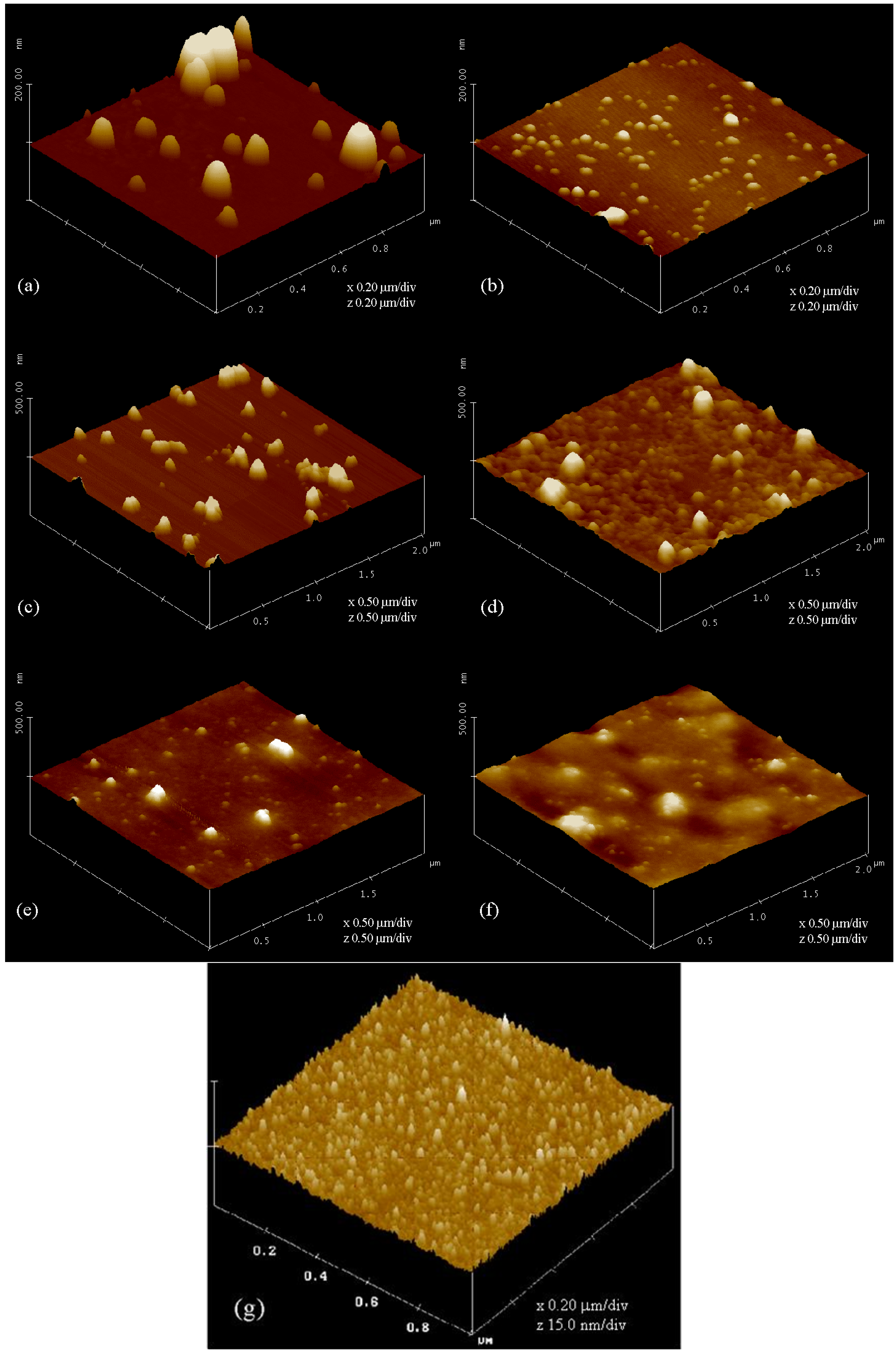
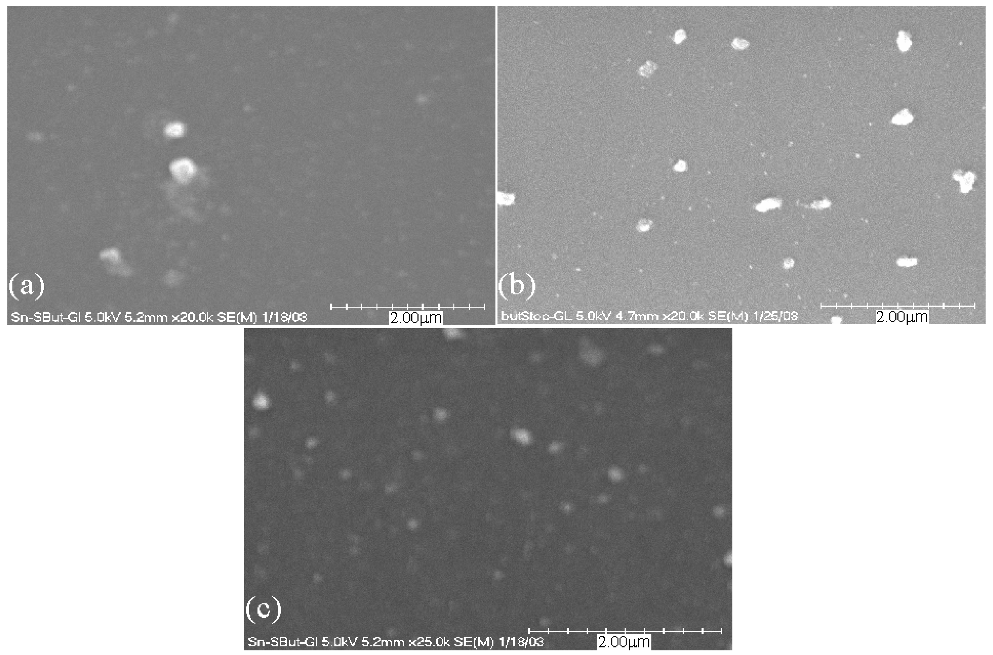
2.1.3. Solution-Phase Deposition of Silver on Sensitized Plane Glass

To probe how the deposition of silver and the evolution of roughness takes place during metal deposition, i.e., mirroring, we conducted similar systematic studies of silver deposition on the surface of deposited SnOx nanoparticles Figure 5a. The z-range of deposited silver increases monotonously with the concentration of silver ions (Figure 5b). The radius of particles in the deposited film increases with concentration, indicating decreased curvature. It is clear nonetheless that the initial high curvature of the silver film is dictated by the curvature and the size of the SnOx nanoparticles that provide necessary chemical reduction and sites for deposition of Ag+ ions. The initial monolayer provides a wetting layer for subsequent growth of the silver film. The deposited silver atoms appear to be mobile and increase the radius of curvature of particles as the film grows to minimize the high metal surface energy (γAg ≈ 900 mJ/m2). Electroless silver deposition on the glass surface bears a striking resemblance to the mound structure observed in the evaporative deposition of silver on the (100) plane of silver crystals [33]. Thus, providing an atomically smooth silver film would require the atomically smooth deposition of SnOx by suppressing the formation of the nanoparticles on the surface.
Figure 5. Effect of silver concentration on the z-range of the deposited silver on SnOx films (a). 1 μm × 1 μm size AFM images of deposited silver at different concentration of AgNO3; x–y, and z scales are 0.2 μm/div and 100 nm/div; (b) z-range of the silver film deposited on the sensitized glass as function of concentration in the solution.
Crystals 05 00116 g005

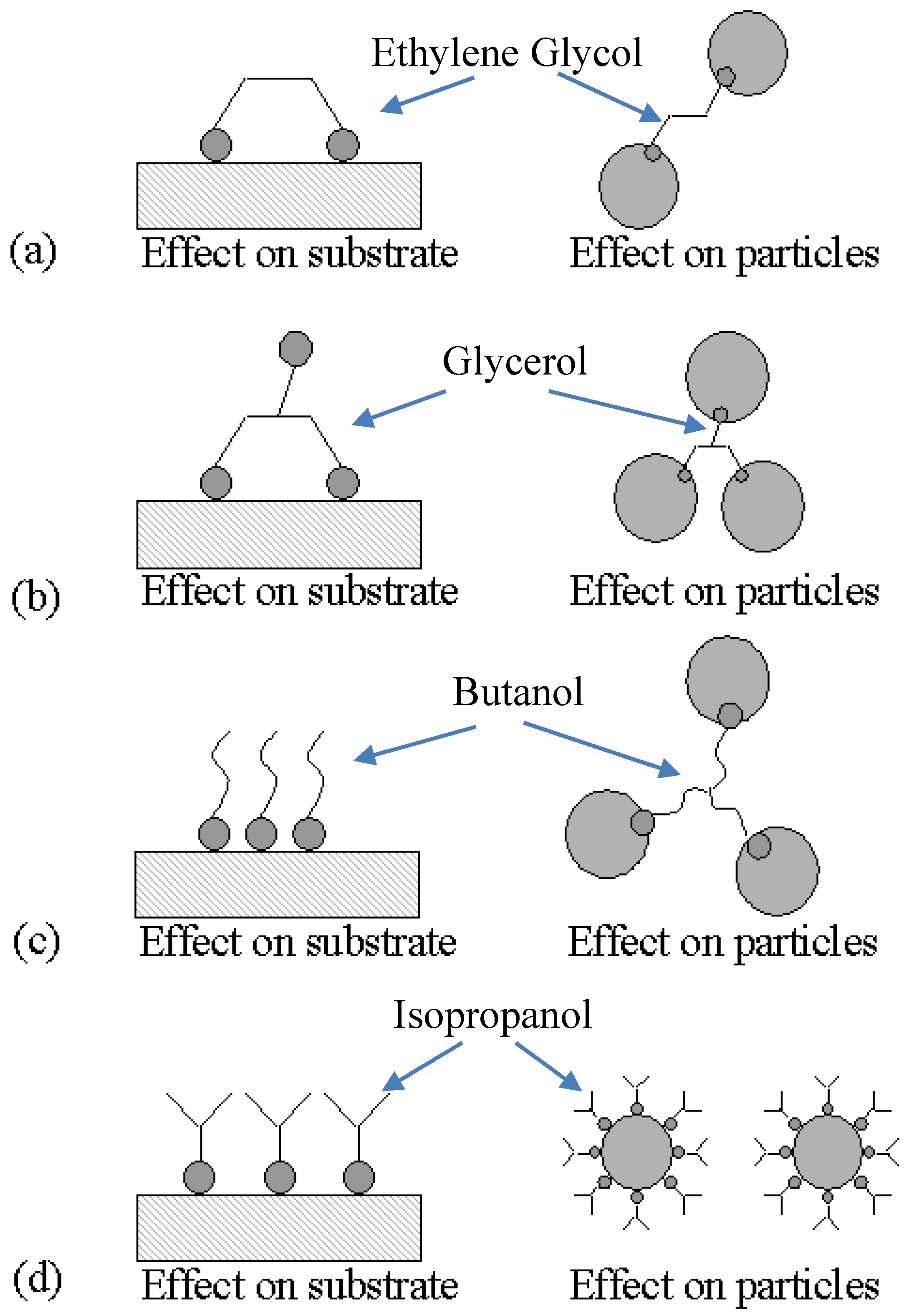
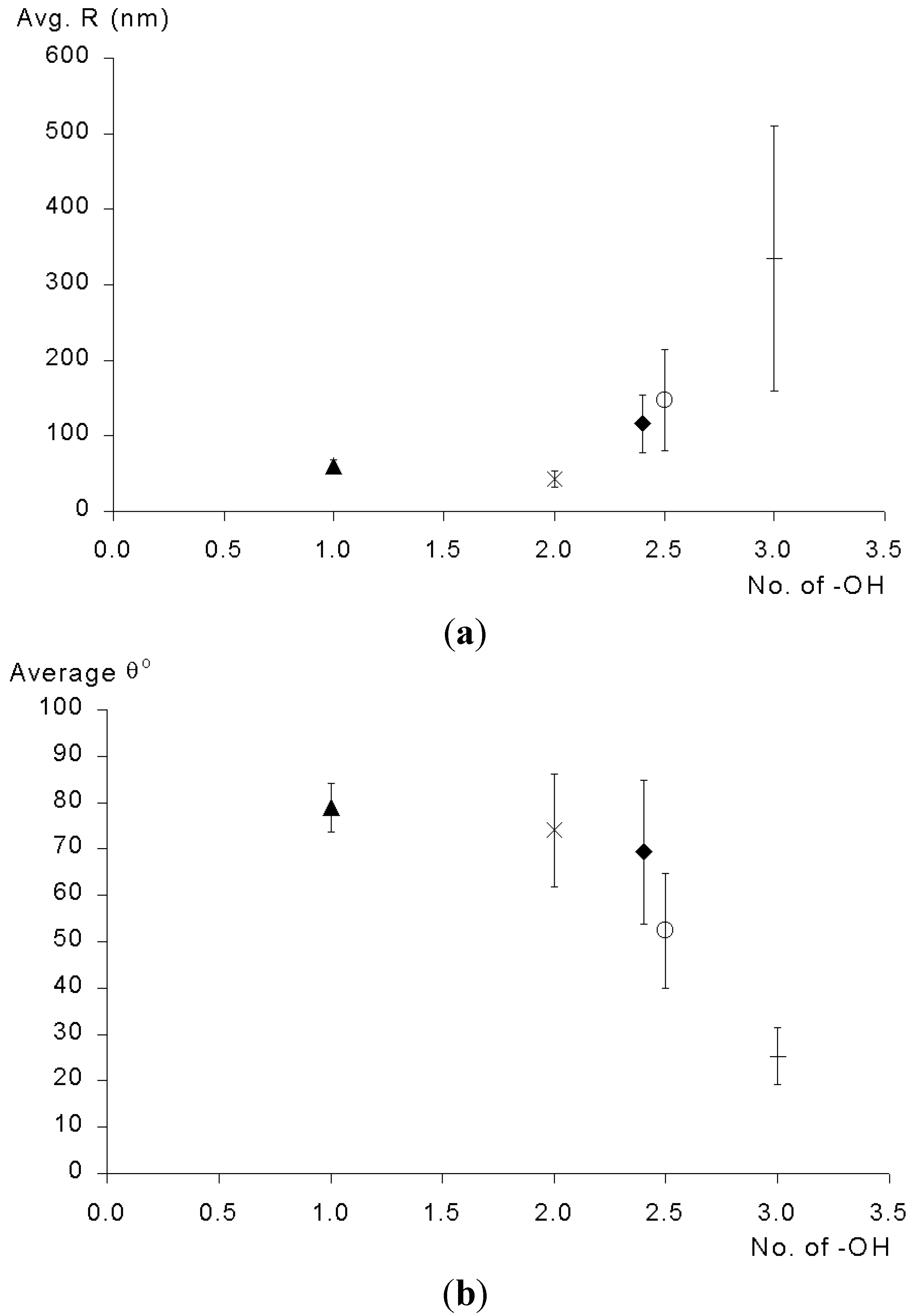
2.1.4. Alcohols Affect the Deposition of SnOx Particles on Glass Surfaces

The independence of particle heights and curvatures, both as functions of deposition time and concentration of SnCl2, implies that the SnOx nanoparticles are likely to be preformed in the sensitizer solution. We therefore examine the influence of alcohols with multiple functional OH groups used as capping and linking agents to control the roughness of the SnOx film. If SnOx is deposited as a molecular species that reorganizes on the surface to form a particulate film then complexation of Sn2+ or Sn4+ ions with alcohols may prevent the growth of particle on the surface, leading to films of even lower z-roughness. If hydrophilic SnOx particles are preformed in the depositing solution, however, then the linking agents would produce even larger aggregates of nanoparticles in the film.
Capping agents introduce possibility of unusually large artifacts caused by binding of clustered nanoparticles to the tip of the AFM probe. Binding of such clusters effectively increases the size of the tip, causing broadening of the imaged clusters. To corroborate our AFM studies we used complementary technique of SEM. Nonconductive SnOx and glass substrates limits the achievable high resolution in SEM because of unavoidable electrostatic charging.
AFM and SEM images presented in Figure 6 and Figure 7 show that alcohols with varying numbers of terminal hydroxyl groups profoundly influence the size and shape of the deposited nanoparticle clusters. Systems containing capping agents generally produce a bimodal distribution of sizes (also see the figure in Section 3) rather than a surface of lower z-roughness. This observation suggests that the SnOx nanoparticles are preformed in the aqueous system.
The different capping agents produce large differences in the characteristics of deposits. The SnOx particles capped in 2-propanol (Figure 6b) show only small, isolated clusters. In contrast, those capped in ethylene glycol show only isolated large clusters (Figure 6a). Other samples reveal bimodal distributions with varying relative proportions of large and small sizes. The larger size aggregates are 100’s of nm in size while the smaller clusters of 30–40 nm size are broadened significantly by the AFM tip effects. Based on AFM z-range measurements shown in Figure 4b,c, both types of clusters are composed of nanoparticles with even smaller sizes (4–7 nm). However, we were unable to confirm the smaller sizes with scanning electron microscopy because of sample charging effects (low electrical conductivity), or with X-ray diffraction [34] because distinct diffraction peaks were absent (amorphous nanoparticles).
These AFM patterns of particles deposited from alcohol containing solutions are very different from what we observe for SnOx films deposited from a sensitizer solution free of the capping agent. For a typical sensitizer concentration (0.027 M), the observed pattern of deposited tin sensitizer is shown in Figure 6g. The z-roughness of these films is 0.6 nm and the z-range over a scanned region of 1 μm × 1 μm is only 4 nm. These dimensions are comparable to the values for the stamped SnOx films shown in Figure 3d.
Figure 6. AFM images of glass SnOx particles bound to glass surfaces and capped with the following different alcohols: (a) ethylene glycol; (b) 2-propanol; (c) 1-butanol; (d) ethylene glycol (0.83 M)/glycerol (0.38 M); (e) ethylene glycol (0.82 M)/glycerol (0.62 M); (f) glycerol; and (g) SnOx from capping agent free SnCl2 (0.027 M) solution. The x–y and z scales in the individual images are as follows: (a,b) 0.2 μm/div; (c,d,e,f) 0.50 μm/div for both x–y and z-axes, respectively; (g) the x–y and z scales are 0.2 μm/div and 15 nm/div.
Crystals 05 00116 g006
Figure 7. SEM images of SnOx particles deposited on glass surfaces, capped in the following different alcohols (a) glycerol; (b) 1-butanol; and (c) ethylene glycol (0.82 M)/glycerol (0.62 M). Sample charging prevented achieving higher resolution. Scale bar = 2 μm.
Crystals 05 00116 g007

2.2. Discussion

These studies show that an inorganic, SnCl2-based sensitizer can replace surfactant SAMs as an ink for controllably depositing silver through microcontact printing. We find little difference between the structural characteristics of the sensitizer films deposited from solution and those printed. The sizes and surface roughness of the deposited and stamped particles (Figure 6g and Figure 3c) are identical. PDMS stamp apparently serves as a neutral medium to transport pre-formed nanoparticles from the sensitizer/ink solution to the glass surface. Given the low surface energy of PDMS and the short residence time (≈1 min) of the sensitizer on the PDMS stamp, this conclusion is not too surprising.
Nevertheless, the method suffers from inherent limitations in achieving very high resolution (<20 nm). These limitations arise from the particulate nature of the sensitizer, which influences the deposition of silver by Tollen’s reaction [35]. Here, we discuss our efforts to modify and model the structure of sensitizer clusters since they directly affect both the lateral and vertical roughness of the subsequently deposited silver.

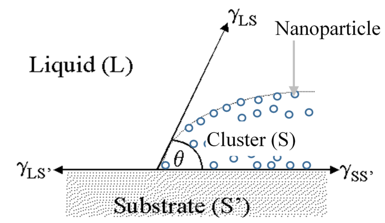
2.2.1. The Nature of the SnOx Clusters on the Glass Surface

Interplay of hydrophilic-hydrophobic interactions and hydrogen bonding between the capping agent, the nanoparticles and the substrate can provide a qualitative explanation of the observed bimodal distribution of cluster sizes (Table 1 and Table 2). When an alcohol is present in the sensitizer, it can functionalize the surfaces of both the glass substrate (Si–OH groups) and the SnOx particles (Sn–OH groups), rendering them either hydrophobic or hydrophilic depending on the molecular structure and the binding geometry of the capping agents as sketched in Figure 8.
Table 1. Mean size and contact angle of small clusters estimated from AFM measurements. Numbers in parenthesis indicate uncertainty (3σ) of the mean.
NumberCapping agentDiameter (nm)Height (nm)Radius (nm)θ°
aEthylene Glycol
b2-Propanol41(5)5(1)44(5)28(3)
c1-Butanol47(9)16(5)26(5)70(10)
dEthylene Glycol (0.83 M)/Glycerol (0.38 M)90(9)30(10)48(4)70(10)
eEthylene Glycol (0.82 M)/Glycerol (0.62)70(10)21(4)40(7)62(7)
fGlycerol49(8)14(3)29(5)59(5)
gWater (0.0076 M SnCl2)
Table 2. Mean size of large clusters extrapolated from measurements by AFM and SEM.
NumberCapping agentDiameter (nm)Height (nm)Radius (nm)θ°
aEthylene Glycol80(20)30(15)40(10)70(10)
b2-Propanol
c1-Butanol120(20) (180(40)) *48(8)60(9)79(6)
dEthylene Glycol (0.83 M)/Glycerol (0.38 M)200(40)70(10)120(40)70(10)
eEthylene Glycol (0.82 M)/Glycerol (0.62)220(70) (220(20)) *49(9)140(70)50(10)
fGlycerol260(70) (280(70)) *28(5)340(170)25(5)
gWater (0.0076 M SnCl2)160(20)4(1)750(90)6(2)
Note: * Values extracted from scanning electron microscopic (SEM) images.
For example, glycerol (butanol) may render both the glass and the SnOx surfaces hydrophilic (hydrophobic). The 2-propanol, having a short and branched alkyl chain, may prevent aggregation of particles. If both the hydroxyl groups of ethylene glycol bind to the glass surface, as shown in Figure 8a, then the resulting hydrophobic surface may hinder binding of isolated hydrophilic nanoparticles. In systems free of capping agents, we observe a close-packed smooth film of particles (Figure 6g) without mounds. Whether the in-plane packing of particles is random or hexagonal closed packed [36,37] remains unknown.
One may view these closed packed films in the aqueous system or the clusters in systems based on capping agents as resulting from a random two or three dimensional packing of nanoparticles during deposition like sand grains piling on a solid surface. The piles of granular materials [38] exhibit a constant spread to height ratio, which defines θ, the angle of repose, equivalent to the contact angle of liquid droplets. The angle of repose results from the friction between the grains and it is given by: tan θ = μF, the dynamic friction coefficient. When a pile of sand has an angle of repose greater than θ, the sand slides and adjusts the slope. The sliding is due to the effect of gravitational force, which is negligible for submicron structures made by the nanometer size particles shown here.
Figure 8. Postulated binding of capping agents with SnOx nanoparticles (large grey spheres) and glass surface (grey box). (a) Ethylene glycol; (b) glycerol; (c) 1-butanol; (d) 2-propanol. Small gray spheres denote alcohol hydrophilic hydroxyl groups. The thin grey lines indicate hydrophobic alkyl groups.
Crystals 05 00116 g008
The ratio of diameter to its height for large clusters (Table 2) varies systematically from ten in glycerol to two for 1-butanol. The ratio increases with the number of hydroxyl groups in the capping alcohol. Thus, we consider another model for nanoparticles clusters deposited on a surface as analogous to immiscible liquid droplets rather than the sand piles discussed above.

2.2.2. Nanoparticle Clusters as Liquid Droplets

The morphology of SnOx films is characteristic of complete wetting of the glass surface with SnOx nanoparticles when deposited from the solutions without capping agent. The space-filling patterns with extremely low roughness suggest self-assembled monolayers of nanoparticles. Similarly, morphology of partial wetting is apparent for the solutions that contain capping agent as reflected in the observed large droplets of nanoparticles (Figure 6a–f). The growth seen here suggests the Volmer-Weber and Stranski-Krastanow patterns of growth [39,40,41] rather than the layer-by-layer epitaxial growth model of Frank-van der Merwe [42] observed in alcohol-free aqueous solutions.
We quantify the shape of SnOx clusters as partially wetting drops commonly observed in molecular liquids on solid surfaces. A fundamental property of a drop on a solid surface is its contact angle. The cluster profile probed by AFM takes the form of a depressed arc with diameter, D, and height, h (Figure 9). From the measured values of D and h, we calculate the effective radius of the cluster, R, and the contact angle, θ, with respect to the surface using the following geometric equations:
R = 1 8 h ( 4 h 2 + D 2 ) ; sin θ = 4 D h ( 4 h 2 + D 2 )
Figure 9. An AFM image of an isolated nanoparticle cluster (left) and a depressed arc representation (right) for determination of its average radius and contact angle.
Crystals 05 00116 g009
Because the AFM tip cannot detect an overhang, these equations are applicable provided that the contact angle is less than 90°. They predict a constant value for the D/h ratio for fixed R and θ. The height and diameter of both small (Table 1) and large (Table 2) clusters, are tabulated separately to determine their R and θ.
Approximating an AFM tip broadening to be 15–20 nm (≈the AFM tip diameter), the measured diameters for the small clusters (Table 1) are considerable larger than the 4–7 nm size of the individual nanoparticles determined from the measured heights (z-range) in Figure 4b,c. Only the small clusters capped in isopropanol display a cluster height comparable to the size of the nanoparticles. In other systems, the heights are at least three-four times larger.
With the exception of 2-propanol, the contact angle, θ ≈ 60° ± 10°, is independent of the capping agent. In the case of isopropanol, as suggested in Figure 8d, the weakness of both inter-particle and particle-substrate interactions lead to small 2d clusters. Because there are large experimental uncertainties in the dimensions of small clusters, our discussion centers mainly on the properties of larger clusters, Table 2. Figure 10 presents the average radius and θ of large clusters plotted with respect to the average number of –OH groups in the capping agent.
Figure 10. Average radius and contact angle of large clusters of SnOx deposited from capping agent containing sensitizer. ▲—1-Butanol; ×—Ethylene glycol; ♦—Ethylene glycol/glycerol(0.83 M/0.38 M); ○—Ethylene glycol/glycerol (0.83 M/0.62 M); and +—glycerol.
Crystals 05 00116 g010
These parameters correlate with the number of OH groups in the capping agent. For large clusters, an increase in R accompanies a decrease in the contact angle θ. For clusters in the solution free of capping agent (Figure 4), the contact angle is <7°, implying that nanoparticles almost completely wet the glass surface. These observations, combined with systematic trends seen in Figure 10, support that the larger clusters act like liquids that produce a contact angle.

2.2.3. Modeling the Distribution of Cluster Sizes Using the Theory of Heterogeneous Nucleation

We further develop the model for growth of a nanoparticle cluster as a nucleating droplet using the classical theory of heterogeneous nucleation. Consider a droplet of radius R defined by its contact angle θ with respect to the supporting solid substrate, Figure 11. The Gibbs free energy for the heterogeneous nucleation is given by [43].
Δ G = γ LS R 2 ( 1 cos θ ) + LS′ γ SS′ R 2 sin 2 θ 1 3 π R 3 [ ( 2 + cos θ) ( 1 cosθ ) 2 ρΔμ ]
Here ρ and Δμ are the number density of nanoparticles and the difference in chemical potential between nanoparticles in the depositing solution and in clusters on the surface. γij denotes an interfacial tension between a pair of phases i and j. L, S and S’ refer to the depositing solution, a cluster of nanoparticles and the glass substrate, respectively.
Figure 11. A nanoparticle cluster is shown as a droplet with a finite contact angle θ with respect to substrate along with different interfacial tensions.
Crystals 05 00116 g011
The Gibbs free energy (Equation (2)) shows a maximum, which represents the nucleation barrier, at a critical radius, RC. Once the cluster size exceeds RC, the cluster can grow indefinitely because the third order term in R drives the free energy to increasingly more negative values [44]. Experimentally, however, the SnOx clusters do not appear to grow beyond a certain size in the presence of capping agents (Figure 6). To account for the quenched growth, we introduce a cluster-cluster, repulsive electrostatic interaction Figure 12 (inset). The additional free energy is positive and scales as the fourth power of the cluster radius, assuming that both clusters have the same size and charge density. The overall free energy becomes:
Δ G = γ LS R 2 ( 1 cosθ ) + LS′ γ SS′ R 2 sin 2 θ 1 3 π R 3 [ ( 2 + cosθ ) ( 1 cosθ ) 2 ρΔμ ] + k R 4
Note that the free energy has second, third and fourth order terms in particles size [45,46]. The free energy exhibits three extreme values: a minimum at R = 0; a maximum at RC (Gibbs’s critical nucleation size); and another minimum at a value of RO > RC, Figure 12.
The result implies that above RO, the cluster size does not grow spontaneously because the repulsive interaction term (kr4) increases, making ΔG > 0 Figure 12. The calculated RO, at the free energy minimum, depends inversely on the magnitude of k. Larger values of k lead to smaller values of RO.
The surface energy and the coefficient of the electrostatic interaction term, k, can be extracted from histogram of the height determined from an AFM image. This analysis requires that we first rewrite Equation (3) in terms of the cluster height h, using Figure 9, D = 2Rsinθ and h = R(1 − cosθ):
Δ G = α h 2 β h 3 + δ h 4
α = LS π ( 1 cosθ ) ( 1 + LS′ γ SS′ ) LS ( 1 + cosθ ) ) ;  β = π 3 Δμρ ( 2 + cosθ ) ( 1 cosθ ) ;  δ = k ( 1 cosθ ) 4
Figure 12. The calculated Gibbs free energy in the presence of repulsive interaction, with γLS = 50 ergs/cm2, γLS − γSS' = 45 ergs/cm2, and k = 0.012 ergs/cm4. The system has a maximum in free energy (the nucleation barrier) at 30 nm and a free energy minimum at 83 nm. Inset shows an electrostatic interaction between clusters A and B, which scales as a product of their respective surface areas.
Crystals 05 00116 g012
Substituting the resulting free energy expression in the Boltzmann equation yields the height distribution function, F(h):
F ( h ) = Ke Δ G / k B T = K e [ α h 2 β h 3 + δ h 4 ] k B T
Here K is a constant. Figure 13 presents a nonlinear least squares fit of Equation (5) to the AFM histogram. As observed, the experimental data are consistent with the model prediction of an asymmetric F(h).
Figure 13. Histogram of heights, measured experimentally as depth fitted to a heterogeneous nucleation model including a repulsive interaction. The dashed line is the best-fit line to the AFM experimental data extracted (noisy line) from the Figure 6d for EG/glycerol system.
Crystals 05 00116 g013
Table 3 presents the best-fit values for the parameters represented in Equation (5) along with the calculated values of interfacial tension γLS, and the electrostatic repulsion parameter, k. We use the approximation that (γLS' − γSS')/2γLS ≤ 1 to calculate γLS from the measured value of α.
Table 3. A nonlinear least squares analysis of the F(h) calculated using the heterogeneous nucleation model including an electrostatic repulsive interaction between nanoparticle clusters. The values in the parenthesis represent the fitting uncertainty in the last significant digit of a given parameter.
Capping agentα/kBT (nm−2)β/kBT (nm−3)δ/kBT (nm−4)γLS (mJ/m2)k × 1011 (mJ/m4 )
Ethylene glycol2.2(1)0.052(2)0.00031 (2)1.02(5)3.5(2)
Propanol3.0(1)0.42(2)0.0144 (5)0.24(1)0.11(4)
Butanol4.5(4)0.12(1)0.00083(8)2.5(2)15(2)
Ethylene glycol + glycerol (0.83 M:0.38 M)0.0192(3)0.00052(8)0.00000352(5)0.005(1)0.0032(1)
Glycerol0.0858(2)0.00472(3)0.0000648(1)0.005(1)0.00021(1)
Water10.5(2)9.1(2)1.94(3)0.057(1)0.00052(2)
The analysis shows that the surface energy between the nanoparticle cluster and depositing solution (γLS) is very small compared to typical values for the interface between molecular fluids and air. The interfacial tension of a liquid with respect to its vapor varies as the fourth power of its number density [44,47,48]. Thus, the number density of nanoparticles in clusters is lower than for molecules in liquids. The difference would give rise to a lower interfacial tension.
Of the different capping agents, glycerol produces clusters with the lowest interfacial tension. The packing density of the nanoparticles in these clusters with respect to the depositing solution must be low. These glycerol-capped nanoparticles wet the glycerol derivatized glass better (Figure 8b) due to favorable hydrogen bonding. Butanol, produces the highest γLS, suggesting that the packing density of nanoparticles in its clusters is higher because of a favorable hydrophobic interaction. As shown in Figure 8c, the relatively hydrophobic glass surface that results from adsorption of butanol would dewet the cluster of hydrophilic nanoparticles. Dewetting is consistent with the high contact angle of these clusters (Table 2). Sensitizer free of capping agent also exhibits a tighter packing of SnOx clusters than the glycerol-based systems. As discussed previously, the system completely wets the glass surface (θ ≈ 0), presumably because of a favorable hydrophilic interaction between nanoparticles and the glass.
The electrostatic parameter, k, scales inversely with the dielectric constant of the capping agents. High dielectric constants, implying low values of k, for glycerol and water enable better screening of the electrostatic interaction (i.e., a lower Debye length), which permits the growth of larger clusters. Butanol, which has the lowest dielectric constant of the different capping agents, would have a longer range of electrostatic repulsion in agreement with the observed high value of k and smaller cluster radius (Table 2). The proposed model accounts for the observed trends in the distributions of cluster height and allows quantification of the surface energy and the electrostatic screening interaction.

2.2.4. Modeling the Cluster Features Using the Theory of Oswald Ripening

Guided by the success of heterogeneous nucleation model, we also considered whether the Lifshitz–Slyozov–Wagner (SLW) model of Oswald ripening [49] could predict the distribution of cluster sizes. The cluster growth is determined by diffusion limited flux (jD) in the Lifshitz–Slyozov model but by kinetically controlled flux (jK) in the Wagner model. If height is normalized relative to hM, the value for which the histogram has a maximum value, such that x = h/hM, then the distribution function, G(x), is given by:
G ( x ) = C x 2 exp ( d / 2 x 3 / 2 ) / [ ( 3 / 2 x ) 2 + 5 d / 9 ( x + 3 ) 1 + 4 d / 9 ]   for  0 < x < 3 / 2
In this expression, d is the dimensionality of crystal nucleation and C is an adjustable constant. For d = 2 or 3 the distribution qualitatively looks similar to the one shown in Figure 13. The equation, however, does not have any adjustable parameters except C. To fit the data, we let the value of d float. Nonlinear least squares analysis lead to the following values of d: butanol, 1.7; ethylene glycol, 1.9; glycerol, 2.2; 2-propanol, 2.4; ethylene glycol + glycerol, 2.5. A recent modification of SLW theory [50,51] allows d to be related to the fraction that diffusion represents of total flux, defined as a = jD/( jD + jK ). The fitted values of d indicate that a diffusion flux has the dominant role in forming a cluster. Better theoretical developments including models of fractal cluster growth are needed to explain the observed values of d, which is beyond the scope of the present work.
To summarize the discussion, a salient feature from these analyses is that the shapes of deposited clusters could be modeled using theories of nucleation. The analogy of nanoparticle clusters to liquid droplet lends further credence to the notion that nanoparticles behave like artificial atoms. Our results show that this view originally based on electronic properties [52], extends to the surface characteristics of the clustered nanoparticles.

3. Experimental Section

3.1. Materials

Elastomeric poly(dimethylsiloxane) (PDMS), was obtained from Silicones, Inc. (P-125 Base QT lot No. 20913 and P-125 Activator QT lot No. 20966, High Point, NC, USA). A commercially available kit (HE-300, Peacock Laboratories, Inc., Philadelphia, PA, USA) used for silver mirroring was employed for EMD of silver films. The stock HE-300 reagents consisted of (A) silver solution (silver nitrate, 0.034 M), (B) activator solution (ammonium hydroxide), (C) reducing agent (formaldehyde) and a sensitizer solution (tin (II) chloride, 0.76 M in water).
The following capping agents were used as received: Ethylene glycol (Aldrich Chemical, cat. No. 32,455-8, St. Louis, MO, USA), glycerol (Aldrich Chemical, cat. No. 13,487-2), 1-butanol (Aldrich Chemical, cat. No. 27,067-9), and 2-propanol (Fisher Chemical, cat. No. A416-4, Pittsburgh, PA 15275, USA).
Deposition studies were performed on microscope cover glass plates (Aldrich Chemical, St. Louis, MO, USA, Corning cover glass, 18 mm × 18 mm × 0.15 mm, cat. No. Z16262-0, average surface roughness < 1 nm), and p-doped silicon wafers (native SiO2 surface) from Wafertech, (Camas, WA, USA). For ease of handling, the thin microscope glass plate was attached to a thicker glass slide (25 mm × 25 mm × 2 mm) using UV curable glue. All glass plates were new and pre-cleaned by sonicating in distilled water.

3.2. Sample Preparation.

3.2.1. Electroless Deposition of Silver

Sensitizer and silvering solutions were prepared fresh daily. The sensitizer (tin (II) chloride, 0.027 M) solution was prepared approximately 15–30 min prior to silver deposition by diluting the concentrated stock solution with distilled water. Silvering reagents (solution A, B and C) were prepared by diluting (1:37 v:v) in distilled water. The three solutions were prepared in different flasks and were not mixed until ready for silver deposition. The silvering (solution A) had Ag+ concentration of 0.91 mM. The sensitizer solution was pipetted over the cleaned microscope glass to cover the entire surface. The microscope glass was sensitized for approximately 20–25 s and then rinsed for 10 s with distilled water. While still wet from rinsing, the sensitized plate was placed horizontally in a small plastic container (95 mm × 105 mm × 22 mm). Equal volumes of diluted reagents A, B, and C were poured into the container to completely submerge the pre-sensitized glass. The container was immediately swirled for 3–4 s for mixing, and then left stagnant for silver deposition. Silver deposition time onto the plate was held constant at 3 min. The plate was then removed from the silvering solution, rinsed with distilled water for 10 s, and left to dry in air. Typical deposition study included at least three samples to gauge the variability in the deposition patterns.

3.2.2. Preparation and Deposition of Capped Catalyst Particles

Alcohols with different numbers of hydroxyl groups and in different structural positions were chosen as capping reagents (Table 4). The capping agent was pipetted into the concentrated (stock) solution of SnCl2. The mixture was sonicated for 3–4 min. Two to three drops of the individual mixtures were placed on a clean glass plates and left standing for 1 min. Two to three droplets were sufficient to prevent it from drying during deposition. Plates were subsequently rinsed with flowing distilled water for 10 s under the tap. The substrates were then air-dried. Preventing adhesion of nanoparticles on the silicon AFM tip required drying for a full day. We routinely observed classic AFM artifacts with imaged objects as large 200–400 nm, caused by the attachment of SnOx particles at distances as high as 5–7 nm from the apex of the tip. Significant binding affinity was verified by depositing SnOx doped with capping agent onto silicon surfaces.
Table 4. Capping agents and their concentration in the sensitizing solutions.
NumberCapping agentMolar concentration in sensitizer SnCl2 (M) *
aEthylene Glycol0.86
b2-Propanol1.2
c1-Butanol0.99
dEthylene Glycol/Glycerol0.83/0.38
eEthylene Glycol/Glycerol0.82/0.62
fGlycerol0.66
Note: * Concentration of the stock SnCl2 solution is 0.76 M.

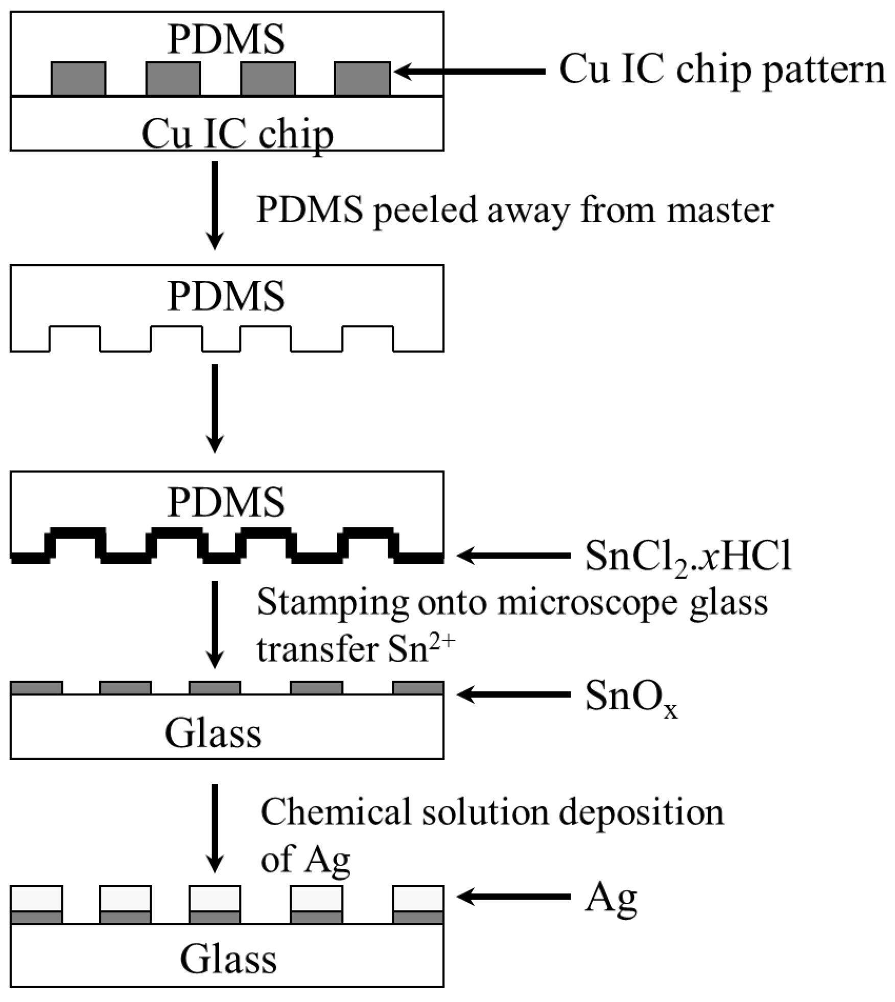
3.2.3. Preparation of PDMS Stamps and Microcontact Printing

The method of preparation PDMS stamps has been extensively discussed by Whitesides et al. [18,19], which was slightly modified in our usage. The elastomeric PDMS stamp was prepared by mixing 3 parts of commercial polymer base to 1 part of activator. The viscous mixture was stirred and evacuated at 100 mTorr to remove trapped air bubbles before pouring. A test copper IC chip used as a master mould created patterns imprinted in PDMS. The surface of the Cu chip was coated with dilute (1 mM) fluorinated surfactant (FC 754) to protect the microstructures from damage when peeling the cured PDMS stamp. The viscous, bubble-free PDMS was slowly poured over the IC chip while taking care to preclude any air pockets from forming at the interface between copper and PDMS. The PDMS was either left to cure overnight in air or baked at 78 °C for 45 min to accelerate curing. Once the PDMS was cured, it was very slowly peeled off vertically to prevent any horizontal shear damage to the microstructures on the IC chip. The stamp was soaked in ethanol for half an hour before use.
The PDMS stamp was inked with sensitizer solution of SnCl2 with one of two methods. The first method involved soaking a cotton Q-tip with ink and spreading the tip over the stamp. The second method employed wetting a high-grade printer paper with ink, and then stamping the paper to transfer ink. Once the stamp was inked, it was left to dry in air for a minute. Drying involved a gentle airflow over the stamp. Once the stamp was nearly dry, it was gently stamped on the microscope glass avoiding excess force to prevent image distortion and smearing. The latent SnOx image was then developed using a silvering solution as described above. The optical, SEM and AFM images of the patterned and developed silver structures appear in Figure 2 and Figure 3.

3.3. Characterization

Three different microscopic techniques were used to image surfaces. These included reflective optical microscopy, atomic force microscopy (Digital Instrument® 3100, Santa Barbara, CA, USA) and scanning electron microscopy (Zeiss DSM-960 and Hitachi S-4700, Pleasanton, CA, USA). The SEM data were collected at beam voltage of 30 kV and current of 14 μA. The AFM used a tapping mode in air with a silicon tip probe (Nanoprobe™, TESP(W), radius of curvature 5–10 nm, spring constant 20–100 N/m, resonant frequency 200–400 kHz, cantilever length 152 μm).

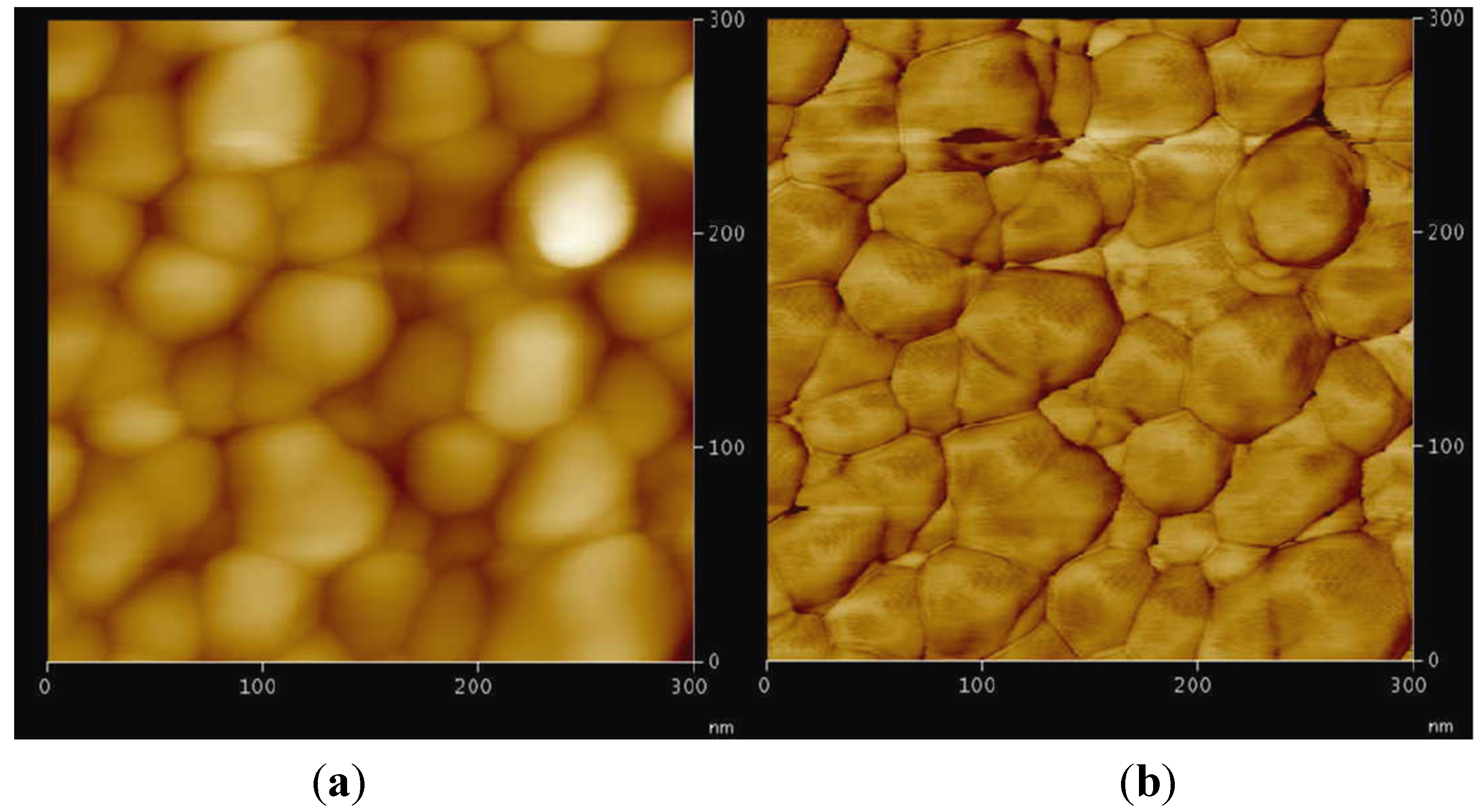
AFM Characterization

Two fundamental limitations of scanning with AFM are: first, the broadening of objects caused by the finite size of tip; and second, the inability to probe structures that have overhang [31,32]. The conical AFM tip design prevents access to overhanging features.
The resolution obtained in the tapping and contact modes should be comparable provided that the spacing between the scan lines is small compared to the radius of the tip. In our studies we typically used step sizes of 2 nm. It is also possible to get an approximate idea of the particle sizes that are smaller than the tip size, if the particle shape profile is known. This requires solving simultaneous equations for the particle shape profile and the profile of the tip to extract the point of first contact between the tip and the particle. We have corrected the lateral dimensions of objects by subtracting the dimension of the tip (i.e., twice the tip radius).
AFM has a much finer dynamic range in the vertical direction. Nevertheless, the bluntness of the tip also affects the smallest features it can probe on densely packed structures. For structures that are much larger than the tip and isolated from each other, corrections in the lateral direction are negligible. Figure 14 shows a 300 nm × 300 nm scan of a silvered glass surface collected in the tapping mode. Note that the phase profile shows a better resolution than the height profile. By considering the dimensions of triangular junctions, we estimated the tip broadening in the height image profile of 15–20 nm, consistent with the broadening expected from the AFM tip.
Figure 14. AFM images of height (a) and phase (b) of Ag nanoparticulate film.
Crystals 05 00116 g014
In analyzing the particle sizes, we used combinations of phase and height images to extract effective dimensions of these structures. This involved averaging dimensions of 50–100 particles selected at random. Increasing the number of averaged particles did not decrease the uncertainty, which was affected mainly by the inherent polydispersity of particle sizes. In several cases, the effect of contaminated tips produced higher broadening (>10 nm). Therefore, we employed SEM imaging to independently confirm the measurements of lateral dimensions.

3.4. Data analysis

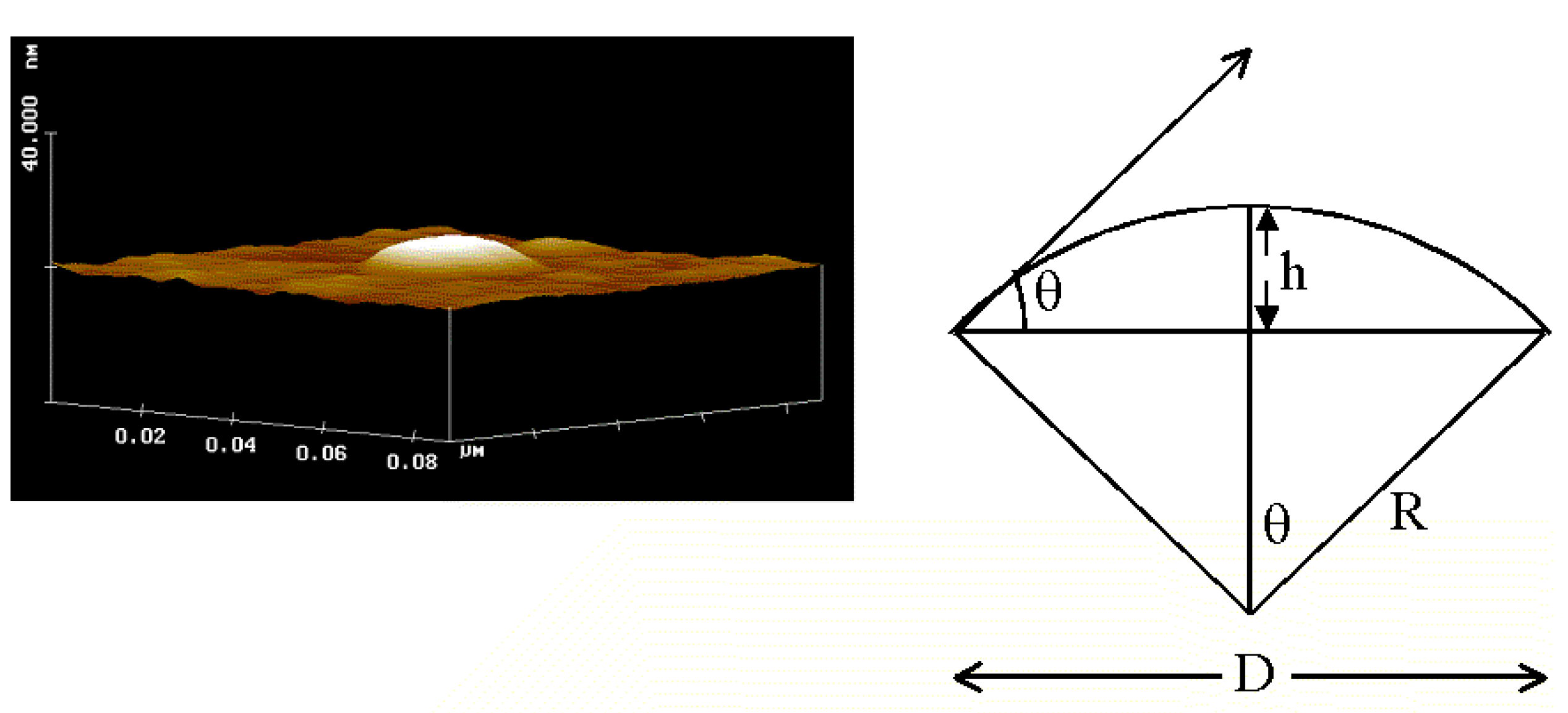
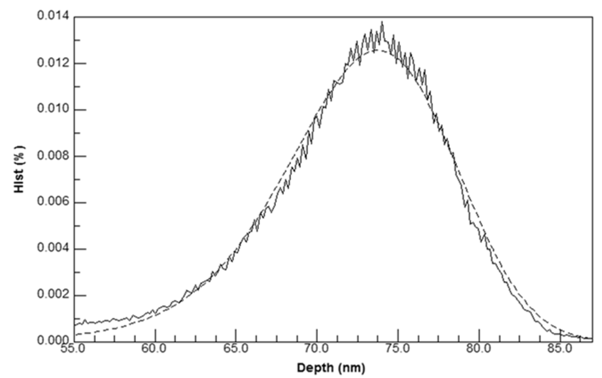
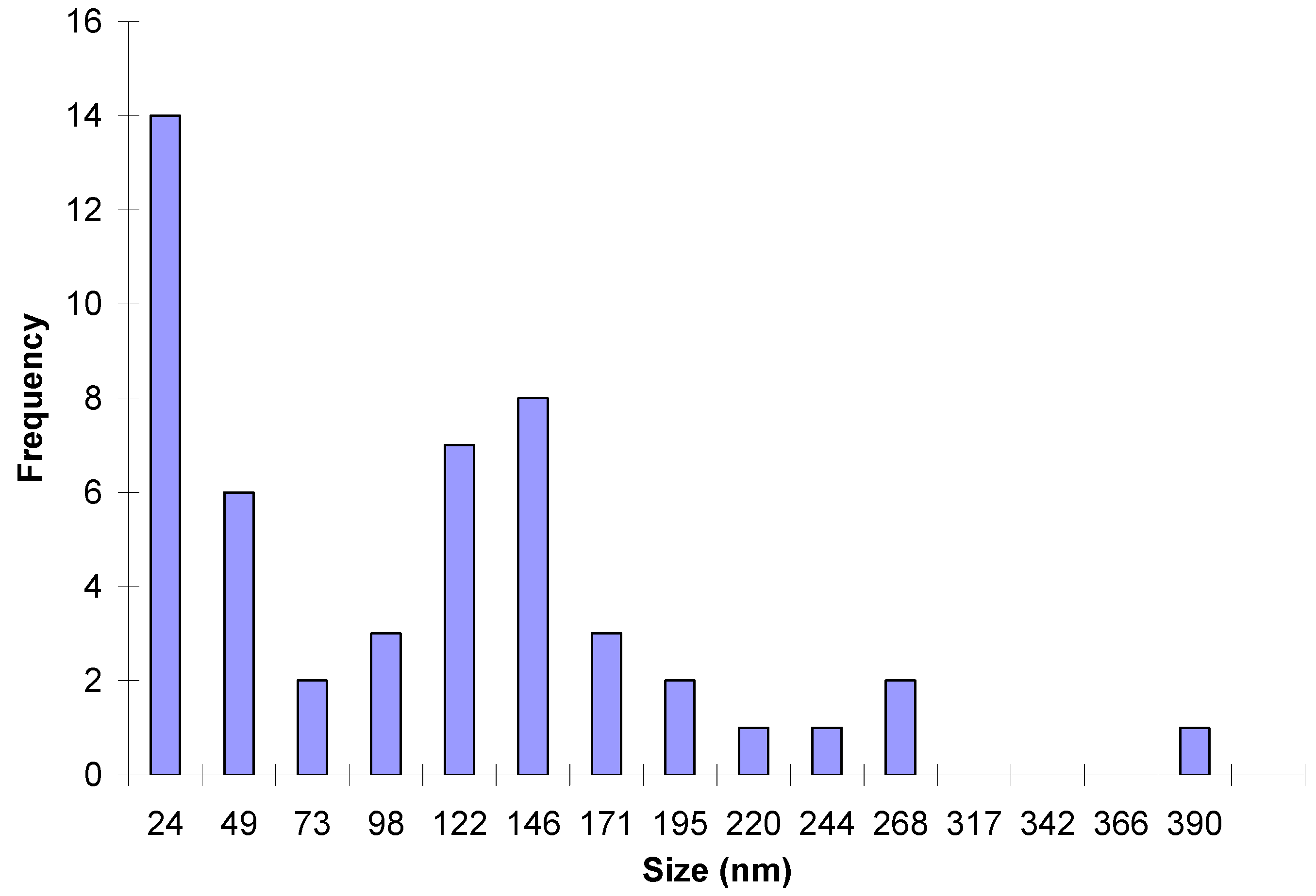
3.4.1. Size and Height Analysis

Figure 15 shows a typical histogram of particle diameters with a bimodal distribution of particle sizes. Table 2 includes the height and width parameters for the group of larger particles in the histogram. The height histogram data for the larger size clusters were used to determine the parameters presented in Table 3 (see below). The AFM tip broadening prevented reliable determination of size distributions for the smaller size clusters shown in Table 1, where only particle counting method was used to extract the raw particle size dimensions.
Figure 15. Projected size distribution for SnOx capped in 1-butanol.
Crystals 05 00116 g015

3.4.2. Nonlinear Least Squares Data Analysis

Fitting data for the F(h) was performed with two different data analysis packages, Genplot™ and PSI-plot™, to confirm convergence. Both the packages use the Marquadt-Levenberg algorithm for fitting. The histogram of heights provided by the vendor (Digital™ nanoscope II) does not provide uncertainties in the z-dimension, so the data analysis used constant data weighting. The analysis used >128 points after 3 point smoothing of the raw data (for large size clusters) to extract four parameters in Equation (5) and three parameters in Equation (6). Typical values of un-normalized χ2 were <10−3 with Equation (5) providing a consistently better fit than Equation (6).

4. Conclusions

The venerable history of mirrors [2] illustrates how a film of SnOx nanoparticles on a glass surface can provide an optically smooth wetting layer for formation of silver mirrors in less than 30 s. Using SnOx as a reactive ink in micro-contact printing enables a controlled deposition of silver in spatially modulated patterns. The SnOx ink, as compared to surfactant-based SAMs, permits EMD for microelectronic applications that require processing at high temperature. The intrinsic linewidth and the surface roughness of deposited silver films, however, are limited by the size of SnOx and Ag nanoparticles. If the size of both silver and SnOx nanoparticles are controlled, a linewidth of ~100 nm is feasible.
The SnOx nanoparticles deposited from an aqueous medium form a close-packed, 4–7 nm thick layer. Capping agents with different numbers of –OH groups can change the nature of the film from a smooth (mono)layer to well-separated islands or clusters. These clusters behave like nucleating droplets on the surface with a characteristic contact angle. A nucleation model including inter-cluster electrostatic interaction can be fitted to the distribution of heights observed by AFM to evaluate electrostatic contributions and surface tension. Silver represents only one example of electroless deposition; other metals such as gold, platinum and copper can also be studied with this approach, and should be pursued in the future for both scientific merit and applications.

Acknowledgments

The financial support of this work through Avery Dennison, Inc. is gratefully acknowledged. We thank Raj Solanki and Jody House for providing access to the AFM facilities. We are grateful to Nabil Mistkawi for SEM imaging. The work was greatly enhanced through many stimulating discussions with John Freeouf and Carl Wamser.

Author Contributions

Joo C. Chan conducted the majority of experiments and data analysis. Nicole Hannah-Moore performed data fitting. Shankar B. Rananavare designed the project and wrote the manuscript.

Conflicts of Interest

The authors declare no conflict of interest.

References and Notes

  1. Liebig, J. Ueber versilberung und vergoldung von glas. Justus Liebigs Ann. Chem. 1856, 98, 132–139. (In German) [Google Scholar] [CrossRef]
  2. Liebig, J.V. Ueber die produkte der oxydation des alkohols, aldehyd. Ann. D. Pharm. 1835, 14, 134–144. (In German) [Google Scholar]
  3. Pratt, J.E. Silvering Mirrors. British Patent 1258, 24 March 1876. [Google Scholar]
  4. Pratt, J.E. Preparing Glass for Silvering. British Patent 1259, 24 March 1876. [Google Scholar]
  5. D’Amico, J.F.; de Angelo, M.A.; Henrickson, J.F.; Kenney, J.T.; Sharp, D.J. Selective electroless metal deposition using patterned photooxidation of Sn2+ sensitized substrates. J. Electrochem. Soc. 1971, 118, 1695–1699. [Google Scholar] [CrossRef]
  6. Wei, X.; Roper, D.K. Tin sensitization for electroless plating review. J. Electrochem. Soc. 2014, 161, D235–D242. [Google Scholar] [CrossRef]
  7. D’Amico, J.F.; DeAngelo, M.A. Sensitizer aging effects on metalization and imaging in the photoselective metal deposition (PSMD) process. J. Electrochem. Soc. 1973, 120, 1469–1475. [Google Scholar] [CrossRef]
  8. D’Amico, J.F.; Litt, F.A.; DeAngelo, M.A. Optical response in the photoselective metal deposition (PSMD) imaging system. J. Electrochem. Soc. 1972, 119, 956–962. [Google Scholar] [CrossRef]
  9. Kind, H.; Geissler, M.; Schmid, H.; Michel, B.; Kern, K.; Delamarche, E. Patterned electroless deposition of copper by microcontact printing palladium complexes on titanium-covered surfaces. Langmuir 2000, 16, 6367–6373. [Google Scholar] [CrossRef]
  10. Ito, H. Chemical amplification resists: History and development within IBM. IBM J. Res. Dev. 1997, 41, 69–80. [Google Scholar] [CrossRef]
  11. Holmes, S.J.; Mitchell, P.H.; Hakey, M.C. Manufacturing with DUV lithography. IBM J. Res. Dev. 1997, 41, 7–19. [Google Scholar] [CrossRef]
  12. Rothschild, M.; Forte, A.R.; Kunz, R.R.; Palmateer, S.C.; Sedlacek, J.H.C. Lithography at a wavelength of 193 nm. IBM J. Res. Dev. 1997, 41, 49–55. [Google Scholar] [CrossRef]
  13. Ausschnitt, C.P.; Thomas, A.C.; Wiltshire, T.J. Advanced DUV photolithography in a pilot line environment. IBM J. Res. Dev. 1997, 41, 21–37. [Google Scholar] [CrossRef]
  14. Wallraff, G.; Hinsberg, W. Lithographic imaging techniques for the formation of nanoscopic features. Chem. Rev. 1999, 99, 1801–1822. [Google Scholar] [CrossRef] [PubMed]
  15. Kaanta, C.W.; Bombardier, S.G.; Cote, W.J.; Hill, W.R.; Kerszykowski, G.; Landis, H.S.; Poindexter, D.J.; Pollard, C.W.; Ross, G.H.; Ryan, J.G.; et al. Dual Damascene: A ULSI Wiring Technology. In Proceedings of Eighth International IEEE VLSI Multilevel Interconnection Conference, Santa Clara, CA, USA, 11–12 Jun 1991; pp. 144–152.
  16. Grill, A.; Hummel, J.P.; Jahnes, C.V.; Patel, V.V.; Saenger, K.L. Dual Damascene Processing for Semiconductor Chip Interconnects. U.S. Patent No. 6,448,176, 10 September 2002. [Google Scholar]
  17. Tricoli, A.; Graf, M.; Mayer, F.; Kuühne, S.; Hierlemann, A.; Pratsinis, S.E. Micropatterning layers by flame aerosol deposition-annealing. Adv. Mater. 2008, 20, 3005–3010. [Google Scholar] [CrossRef]
  18. Xia, Y.; Rogers, J.A.; Paul, K.E.; Whitesides, G.M. Unconventional methods for fabricating and patterning nanostructures. Chem. Rev. 1999, 99, 1823–1848. [Google Scholar] [CrossRef] [PubMed]
  19. Xia, Y.; Whitesides, G.M. Soft lithography. Angew. Chem. Int. Ed. 1998, 37, 550–575. [Google Scholar] [CrossRef]
  20. Biebuyck, H.A.; Larsen, N.B.; Delamarche, E.; Michel, B. Lithography beyond light: Microcontact printing with monolayer resists. IBM J. Res. Dev. 1997, 41, 159–170. [Google Scholar] [CrossRef]
  21. Li, Z.; Gu, Y.; Wang, L.; Ge, H.; Wu, W.; Xia, Q.; Yuan, C.; Chen, Y.; Cui, B.; Williams, R.S. Hybrid nanoimprint-soft lithography with sub-15 nm resolution. Nano Lett. 2009, 9, 2306–2310. [Google Scholar] [CrossRef] [PubMed]
  22. Kumar, A.; Biebuyck, H.A.; Whitesides, G.M. Patterning self-assembled monolayers: Applications in materials science. Langmuir 1994, 10, 1498–1511. [Google Scholar] [CrossRef]
  23. Xia, Y.; Kim, E.; Mrksich, M.; Whitesides, G.M. Microcontact printing of alkanethiols on copper and its application in microfabrication. Chem. Mater. 1996, 8, 601–603. [Google Scholar] [CrossRef]
  24. Tate, J.; Rogers, J.A.; Jones, C.D.; Vyas, B.; Murphy, D.W.; Li, W.; Bao, Z.; Slusher, R.E.; Dodabalapur, A.; Katz, H.E. Anodization and microcontact printing on electroless silver: Solution-based fabrication procedures for low-voltage electronic systems with organic active components. Langmuir 2000, 16, 6054–6060. [Google Scholar] [CrossRef]
  25. Rogers, J.A.; Bao, Z.; Baldwin, K.; Dodabalapur, A.; Crone, B.; Raju, V.; Kuck, V.; Katz, H.; Amundson, K.; Ewing, J. Paper-like electronic displays: Large-area rubber-stamped plastic sheets of electronics and microencapsulated electrophoretic inks. Proc. Natl. Acad. Sci. USA 2001, 98, 4835–4840. [Google Scholar] [CrossRef] [PubMed]
  26. Chan, J.C. Fundamental Studies of SnO2 and Ag Nanoparticles: Growth, Kinetics and Applications. Master’s Thesis, Portland State University, Portland, OR, USA, February 2002. [Google Scholar]
  27. Coleman, J.P.; Lynch, A.T.; Madhukar, P.; Wagenknecht, J.H. Antimony-doped tin oxide powders: Electrochromic materials for printed displays. Sol. Energy Mater. Sol. Cells 1999, 56, 375–394. [Google Scholar] [CrossRef]
  28. Chan, J.C.; Hannah, N.A.; Rananavare, S.B.; Yeager, L.; Dinescu, L.; Saraswat, A.; Iyer, P.; Coleman, J.P. Mechanisms of aging of antimony doped tin oxide based electrochromic devices. Jpn. J. Appl. Phys. Part 2 2006, 45, L1300–L1303. [Google Scholar] [CrossRef]
  29. Chaparadza, A.; Rananavare, S.B.; Shutthanandan, V. Synthesis and characterization of lithium-doped tin dioxide nanocrystalline powders. Mater. Chem. Phys. 2007, 102, 176–180. [Google Scholar] [CrossRef]
  30. Electron microscopic and X-ray studies of these particle sizes clearly show nanocrystals (3–8 nm in size) but only after calcinations at high temperature (500–800 °C); a cassiterite lattice structure corresponding to SnO2 is observed [28,29].
  31. Gibson, C.; Watson, G.; Myhra, S. Scanning force microscopy calibrative procedures for best practice. Scanning 1997, 19, 564–581. [Google Scholar] [CrossRef]
  32. Keller, C.B.A.D. Scanning force microscopy in biology. Phys. Today 1995, 48, 32–38. [Google Scholar]
  33. Caspersen, K.J.; Layson, A.R.; Stoldt, C.R.; Fournee, V.; Thiel, P.A.; Evans, J.W. Development and ordering of mounds during metal (100) homoepitaxy. Phys. Rev. B 2002, 65. [Google Scholar] [CrossRef]
  34. Patterson, A.L. The Scherrer formula for X-ray particle size determination. Phys. Rev. 1939, 56, 978–982. [Google Scholar] [CrossRef]
  35. Shakhashiri, B.Z. Chemical Demonstrations: A Handbook for Teachers of Chemistry; The University of Wisconsin Press: Madison, WI, USA, 1992; Volume 4, pp. 240–243. [Google Scholar]
  36. Teranishi, T. Metallic Colloids; Marcel Dekker: New York, NY, USA, 2002. [Google Scholar]
  37. Shimizu, T.; Teranishi, T.; Hasegawa, S.; Miyake, M. Size evolution of alkanethiol-protected gold nanoparticles by heat treatment in the solid state. J. Phys. Chem. B 2003, 107, 2719–2724. [Google Scholar] [CrossRef]
  38. Lee, J.; Herrmann, H.J. Angle of repose and angle of marginal stability: Molecular dynamics of granular particles. J. Phys. A 1993, 26. [Google Scholar] [CrossRef]
  39. Volmer, M.; Weber, A. Keimbildung in übersättigten gebilden. Z. Phys. Chem. 1926, 119, 277–301. (In German) [Google Scholar]
  40. Stranski, N.; von Krastanow, L. Sitzungsberichte der akademie der wissenschaften in wien. Akad. Wiss. Lit. Mainz Math. Natur. Kl. Iib 1939, 146, 797–810. (In German) [Google Scholar]
  41. Luth, H. Surfaces and Interfaces of Solid Materials, 3rd ed.; Springer Verlag: Heidelberg, Germany, 1995. [Google Scholar]
  42. Frank, F.C.; van der Merwe, J.H. One-dimensional dislocations. I. Static theory. Proc. R. Soc. Lond. Ser. A 1949, 198, 205–216. [Google Scholar] [CrossRef]
  43. Navascuas, G.; Tarazona, P. Line tension effects in heterogeneous nucleation theory. J. Chem. Phys. 1981, 75, 2441–2446. [Google Scholar] [CrossRef]
  44. Adamson, A.W.; Gast, A.P. Physical Chemistry of Surfaces, 6th ed.; Wiley Interscience Publication: New York, NY, USA, 1997. [Google Scholar]
  45. De Gennes, P.G.; Prost, J. The Physics of Liquid Crystals, 2nd ed.; Oxford Science Publications: Oxford, UK, 1993; Volume 83. [Google Scholar]
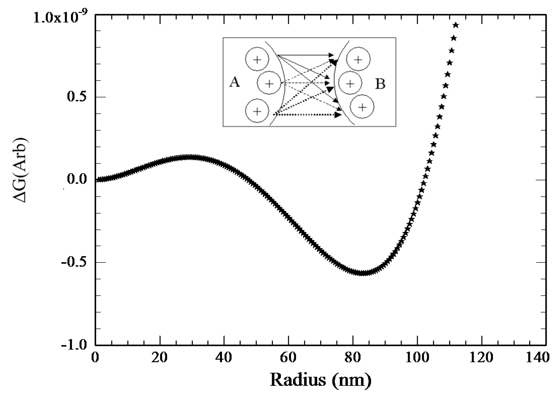
  46. This expansion of free energy as a power series in R is analogous to the order parameter expansion for the free energy of the nematic to isotropic (NI) liquid crystal phase transition [45]. The power series expansion for the NI transition has a negative, third order term in the order parameter making the transition first order, as is also the case for the bulk solid-liquid phase transition due to a similar third order term. The first order nature of these transitions is indicated by a two-phase coexistence at the phase transition. We suggest that the nucleation of nanoparticle clusters on the glass surface is a weakly first order phase transition with a scaled cluster size acting as an order parameter. At the phase transition, large clusters on the surface coexist with smaller clusters in solution or on the surface. A second order phase transition (i.e., without two phase coexistence) is expected when the contact angle, θ, vanishes removing the cubic term in Equation (3).
  47. Kirkwood, J.G.; Buff, F.P. The statistical mechanical theory of surface tension. J. Chem. Phys. 1949, 17, 338–343. [Google Scholar] [CrossRef]
  48. Macleod, D.B. On a relation between surface tension and density. Trans. Faraday Soc. 1923, 19, 38–41. [Google Scholar] [CrossRef]
  49. Yao, J.H.; Elder, K.R.; Guo, H.; Grant, M. Theory and simulation of ostwald ripening. Phys. Rev. B 1993, 47, 14110–14125. [Google Scholar] [CrossRef]
  50. Baldan, A. Review progress in ostwald ripening theories and their applications to nickel-base superalloys part I: Ostwald ripening theories. J. Mater. Sci. 2002, 37, 2171–2202. [Google Scholar] [CrossRef]
  51. Vengrenovich, R.D.; Ivanskii, B.V.; Panko, I.I.; Yarema, S.V.; Kryvetskyi, V.I.; Stasyk, M.O. Ostwald ripening of the platinum nanoparticles in the framework of the modified LSW theory. J. Nanomater. 2014, 2014. [Google Scholar] [CrossRef]
  52. Kastner, M.A. Artificial atoms. Phys. Today 1993, 1, 24–31. [Google Scholar] [CrossRef]

