
Recent Advances in Two-Dimensional Materials with Charge Density Waves: Synthesis, Characterization and Applications
by
 ,
,
Mongur Hossain
1,2 ,
,
Zhaoyang Zhao
1,2,
Wen Wen
1,2,
Xinsheng Wang
1,
Juanxia Wu
1 and
Liming Xie
1,2,* 1
CAS Key Laboratory of Standardization and measurement for Nanotechnology, CAS Center for Excellence in Nanoscience, National Center for Nanoscience and Technology, Beijing 100190, China
2
University of Chinese Academy of Sciences, Beijing 100190, China
*
Author to whom correspondence should be addressed.
Crystals 2017, 7(10), 298; https://doi.org/10.3390/cryst7100298
Submission received: 10 August 2017
/
Revised: 25 September 2017
/
Accepted: 26 September 2017
/
Published: 3 October 2017
(This article belongs to the Special Issue Two-Dimensional Materials beyond Graphene and their Van der Waals Heterostructures)
Abstract
:Recently, two-dimensional (2D) charge density wave (CDW) materials have attracted extensive interest due to potential applications as high performance functional nanomaterials. As other 2D materials, 2D CDW materials are layered materials with strong in-plane bonding and weak out-of-plane interactions enabling exfoliation into layers of single unit cell thickness. Although bulk CDW materials have been studied for decades, recent developments in nanoscale characterization and device fabrication have opened up new opportunities allowing applications such as oscillators, electrodes in supercapacitors, energy storage and conversion, sensors and spinelectronic devices. In this review, we first outline the synthesis techniques of 2D CDW materials including mechanical exfoliation, liquid exfoliation, chemical vapor transport (CVT), chemical vapor deposition (CVD), molecular beam epitaxy (MBE) and electrochemical exfoliation. Then, the characterization procedure of the 2D CDW materials such as temperature-dependent Raman spectroscopy, temperature-dependent resistivity, magnetic susceptibility and scanning tunneling microscopy (STM) are reviewed. Finally, applications of 2D CDW materials are reviewed.
1. Introduction
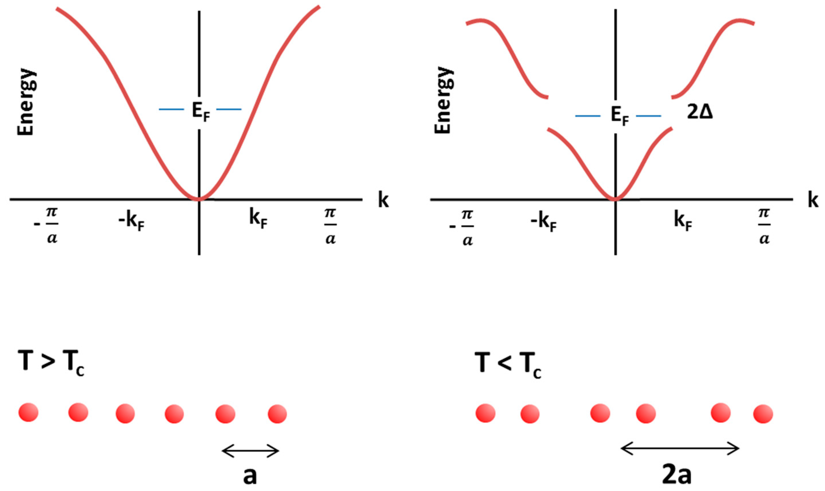
Recent breakthroughs in the synthesis techniques of 2D layered materials have facilitated the exploration of materials systems that were challenging in the past [1,2,3]. Transition metal dichalcogenides (TMDs) are a group of layered materials that has renewed interest due to their 2D confined structures [4,5]. TMDs disclose a variety of fascinating properties including semiconducting [6,7,8], superconducting [9], charge density waves (CDWs) [10,11], and so on. CDW is a ground state with a periodic modulation of charge density associated with a periodic distortion of the crystal lattice [12,13,14,15,16,17]. The transition to the CDW state usually is depicted as the consequence of Fermi surface nesting with wave vector Q = 2kF and exhibits an energy gap at Fermi energy in the quasi-1D counterpart (Figure 1) [18,19,20].
Several TMDs (in the form of X-M-X, M = V, Nb, Ta, Ti and X = S, Se or Te) with the chalcogen atoms in two hexagonal planes separated by a plane of metal atoms in the middle comprise a major family of 2D CDW materials. Adjacent layers in X-M-X are weakly bonded together, which can have different metal atom coordinations within the layer and different stacking between layers (Figure 2). The coordination configurations of metal atoms in 2D CDW materials can be octahedral (T) or trigonal prismatic (H). The phase transition with temperature of bulk CDW materials is summarized in Table 1. A variety of CDW phases such as commensurate CDW (C-CDW), nearly-commensurate CDW (NC-CDW) and incommensurate CDW (IC-CDW) can subsist at different temperatures.
In spite of more than three decades of comprehensive experimental and theoretical attempts, the driving force for the CDW transition remains arguable. Upon intercalation with copper [32], selenium [33], tellurium [34], iron [35] or applying pressure [36], the CDW ordering melts, and superconductivity emerges with a critical transition temperature of several Kelvin, which directly indicates the competition between CDW and superconductivity in 2D CDW materials.
In atomically thin 2D CDW materials, phase transitions can steer huge changes in electronic structure and then allow novel electronic devices. Electronic applications such as oscillators [37] and nonvolatile memory storage [38,39] have been demonstrated successfully in recent years, based on the charge density wave phase transitions. Although the investigations of bulk CDW materials have been done extensively for decades, as atomically thin materials, their role is simply up to date. In this review, we summarize the recent study on 2D CDW materials, including the synthesis, characterization and potential applications.
2. Synthesis of 2D CDW Materials
2.1. Mechanical Exfoliation of Bulk Materials
The first cleaving NbSe2 samples with the scotch tape method were reported much earlier by R. F. Frindt in 1972 [40]. However, thinner layers of 2D CDW materials, such as 1T-TaS2 [41,42], 2H-TaS2 [27], 1T-TaSe2 [42], 2H-TaSe2 [31], 2H-NbSe2 [43] and 1T-TiSe2 [11], have been reported recently by the mechanical exfoliation technique.
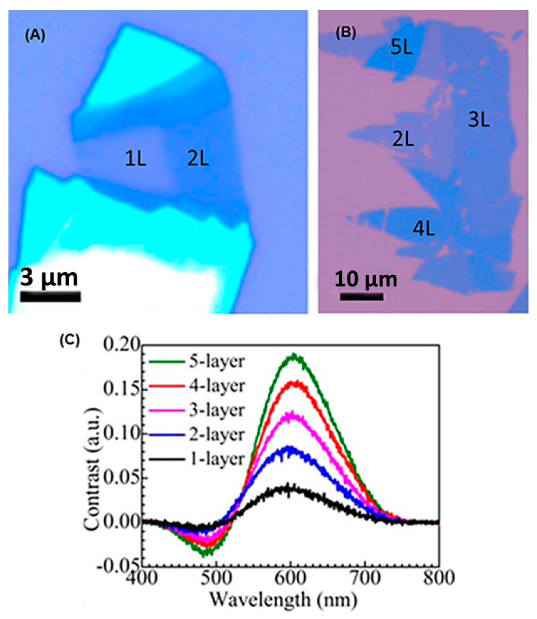
Figure 3 shows the first successful exfoliation of a tantalum diselenide (2H-TaSe2) monolayer and a few layers reported by P. Hyziyev et al. [31]. Using the conventional scotch tape procedure, thinner layers of TaSe2 samples were exfoliated onto 300 nm SiO2/Si substrates. Both white light contrast spectroscopy (WLCS) and atomic force microscopy (AFM) were used to identify the number of layers. The confirmation of the thin layers’ number can be difficult by AFM due to contamination and oxidation, usually if the samples have been exposed to surrounding air for a long time.
2.2. Liquid Exfoliation Method
The liquid exfoliation method has shown its potential to prepare 2D ultrathin nanosheets of layered compounds, such as VS2 [44], VSe2 [4], TaS2 [45], TaSe2 [46] and NbSe2 [46]. In a procedure of liquid exfoliation of VS2 [44] (Figure 4), the VS2·NH3 precursor with NH3 molecules is interpolated into the S-V-S layers. Diffusion of NH3 molecules apart from the stacked layers breaks down the c axis periodicity. Then, ultrathin VS2 nanosheets are formed. A big advantage of the liquid exfoliation method is escaping the high-temperature, time-devouring solid-state procedure, as well as complicated equipment. It also offers high operational accessibility and a short reaction time.
In addition, another emerging method is electrochemical exfoliation. By fabricating a field effect transistor structure using an electrolyte as a gate medium and employing a comparatively high gate voltage, layered materials can be etched layer-by-layer, then leaving an ultrathin or even single-layered film. This technique was reported for the preparation of FeSe (a high-Tc superconductor) [47] and 2H-NbSe2 [48].
2.3. Chemical Vapor Transport
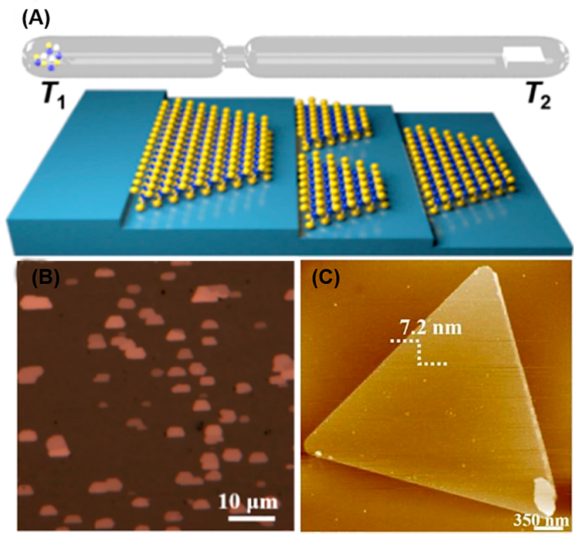
Chemical vapor transport (CVT) is a reliable technique for both research and commercial purposes to grow high quality TMD single crystals [49]. CVT growth of single crystals of TMDs associates the volatilization and reactions of solid precursors with the benefit of transport agents. Deposition of products in the form of single crystals is driven by a temperature gradient between the source and the growth regions [49]. Bulk CDW materials such as 1T-VSe2 [50], 1T-TaSe2 [28], 2H-TaSe2 [5,51] and 2H-NbSe2 [52] have been reported by the CVT method in recent years. For synthesis of 2D CDW materials, recently, J. Wang et al. reported controlled synthesis of two-dimensional 1T-TiSe2 on sapphire substrates with sub-10-nm thickness [53] (Figure 5). It is essential to introduce a growth substrate to guide the 2D growth of TMDs and dramatically slow down the growth of the bulk counterpart in the CVT method.
2.4. Chemical Vapor Deposition
The CVD method is also considered as one of the main processing methods to synthesis 2D materials. CVD involves chemical reactions of gaseous reactants on a heated substrate surface [54,55]. The CVD approach has been used successfully in synthesizing 1T-VS2 [56,57], 1T-VSe2 [58,59], 2H-NbS2 [60], 3R-NbS2 [60], 2H-NbSe2 [61], 1T-TaS2 [62,63], 1T-TiSe2 [64], and so on. Contamination-free and high crystalline quality samples with potential for scaling-up are the great advantages of the CVD method [65].
Later, W. Fu et al. reported the controlled synthesis of atomically-thin 1T-TaS2 [62] (Figure 6). The tantalum pentachloride (TaCl5) and sulfur (S) powder were used as precursors. As the carrier gas, a mixture of N2 with 10% of H2 was used. The reaction was usually carried out at 820 °C. In CVD synthesis, the system pressure, gas flow rate, precursor concentration, vaporization temperature of precursors, reaction temperature and deposition time play the key roles in controlling the quality of the crystals.
2.5. Molecular Beam Epitaxy
MBE technique has also been employed to prepare monolayer and few-layers of 2D CDW materials, such as TiSe2 [66,67], NbSe2 [68,69] and TaS2 [70] since the 1980s. The advantage of MBE growth is that it can produce a large area film with an uniform thickness. Furthermore, MBE gives an exceptionally low concentration of defects, which is extremely preferred in high performance electronic applications.
3. Characterization of 2D CDW Materials
3.1. Raman Spectroscopic Characterization
Temperature-dependent Raman spectroscopy is a powerful tool to understand the vibrational properties of 2D CDW materials. In recent years, temperature-dependent Raman spectra of 1T-VSe2 [71], 1T-TaS2 [72], 1T-TaSe2 [28], 2H-TaSe2 [31,73], 1T-TiSe2 [11] and 2H-NbSe2 [10] have been reported. In addition, Raman spectroscopy has been used vastly to investigate stacking order [74,75], number of layers [76], molecular doping [77], edge orientations [78,79], strain effects [80,81] and other properties of 2D materials.
TMDs with a metallic property can show Peierls transition by forming a superlattice over the underlying crystal lattice at definite critical temperatures. As a result, the overall energy of the system can be lowered [82,83]. Figure 7 depicts the temperature-dependent Raman spectra of 1T-TaSe2 and 2H-TaSe2 samples in the temperature ranges of 213–493 K and 80–300 K, respectively. Bulk 1T-TaSe2 crystals transform into the commensurate charge density wave (C-CDW) at 473 K and incommensurate charge density wave (IC-CDW) at 600 K [28]. The strong changes in the Raman spectra at around 473 K for 1T-TaSe2 can be seen (Figure 7A). Two Raman peaks (177 and 187 cm−1) of 1T-TaSe2 merge together, forming one broad peak, and their intensity also reduced as the material enters into the IC-CDW phase. It is noticeable that, at 473 K (I-CDW phase), the spectra of 1T-TaSe2 appear more as continua than sets of narrow peaks. This property could be elucidated by symmetry considerations. In the IC-CDW state, the translation equilibrium of the lattice vanishes, and the components of the phonon momentum are no longer favorable quantum numbers when it became parallel to the IC-CDW distortions. In the case of a thin sample (35 nm) (Figure 7B), it is also observed that the two Raman peaks commence merging, but the transition temperature is lower (413 K). These data clearly show that the transition temperature between the C-CDW and IC-CDW phases decreases for thinner 1T-TaSe2 film.
Bulk 2H-TaSe2 has a transition from the normal metal phase to the IC-CDW phase at 123 K, followed by the C-CDW phase transformation at 90 K [31,73]. From Figure 7C, the intensities of the two-phonon peak and E2g mode of 2H-TaSe2 lessen with decreasing temperature. In contrast, with reducing temperatures, the intensity of the two-phonon mode (E1g) expands. This feature can be interpreted as when reducing the background signal from the two phonon procedure that increases the visibility of this peak and also the strain-instigated effects due to dissimilarity in thermal expansion coefficients of thinner films and substrate [84,85]. The frequency changes of two-phonon modes for monolayer, bilayers and bulk samples are plotted as a function of temperature (Figure 7D), showing frequency jumps at 120 K, which also indicates the existence of the IC-CDW state in the thinner crystals of 2H-TaSe2.
3.2. Temperature-Dependent Resistivity and Magnetic Susceptibility
Temperature-dependent resistivity and magnetic susceptibility measurements are often used for probing the CDW property. As the temperature changes, an unusual response in resistivity and magnetic susceptibility has been observed in typical CDW material systems, such as 1T-VS2 [21], 1T-VSe2 [4,50,59], 1T-TaS2 [26,37,86] and 1T-TaSe2 [82] which is also an indication of CDW transition.
The thickness plays an important role in the CDW phase transition of 2D CDW materials. The thickness dependence of the NC-CDW to C-CDW phase transition temperature in 1T-TaS2 thin flakes had been reported by M. Yoshida et al. for the first time [87]. Figure 8A illustrates the temperature-dependent electrical resistivity of 1T-TaS2 for various thicknesses. The dimensionality effect on CDW states in 1T-TaS2 was analyzed by investigating pristine thin flakes by changing the thicknesses up to ∼2 nm [26,88]. It was demonstrated that both C-CDW/NC-CDW and NC-CDW/IC-CDW phase transitions are dynamically regulated for varying the sample thickness. As the sample is thinned, both transitions shifted to low temperatures and then instantly disappeared at critical thicknesses of ∼10 nm and ∼3 nm, respectively. The dielectric surrounding and surface contaminations may also have a role in the critical thicknesses, because thin samples are subject to extreme impacts from surface effects owing to the expanded surface-area-to-volume ratio. Additionally, CDW transition temperatures have been successfully tuned by using an ionic liquid as the gate medium in 1T-TaS2-based field effect transistors (FET) [87].
Temperature-dependent resistivity of 1T-VSe2 crystals with thickness ranging from 11.6–66 nm is shown in Figure 8B. The transition temperature decreases from 105 K in bulk form to 81.8 K in the 11.6-nm thicker flake. For 1T-VSe2 flakes, at the phase transition temperature, resistivity shows an upturn kink due to the CDW transition.
In contrast to 1T-TaS2 and 1T-VSe2, it is also reported that the CDW phase transition temperature can increase in the thinner materials. For instance, the liquid-exfoliated 4–8 layer-thick 1T-VSe2 sample shows the CDW phase transition temperature at 135 K, whereas the bulk sample shows it at 107 K [4]. A similar phenomenon has been observed from mechanically-exfoliated TiSe2 samples, where the transition temperature increases from 200–240 K, while thinning the thickness from the bulk to a few nanometers [11]. Moreover, X. Xi et al. reported the strongly enhanced CDW order in atomically-thin NbSe2 TCDW > 100 K for the exfoliated monolayer sample [10], while M. Ugeda et al. observed slightly weakened CDW order (TCDW ∼ 25 K) in the single layer NbSe2 grown on graphene by the MBE method [68]. These dissimilarities of the transition temperature still are not well understood. The sample quality, substrates and the fabricated device status could play crucial roles in CDW phase transitions.
3.3. Scanning Tunneling Microscopic Characterization
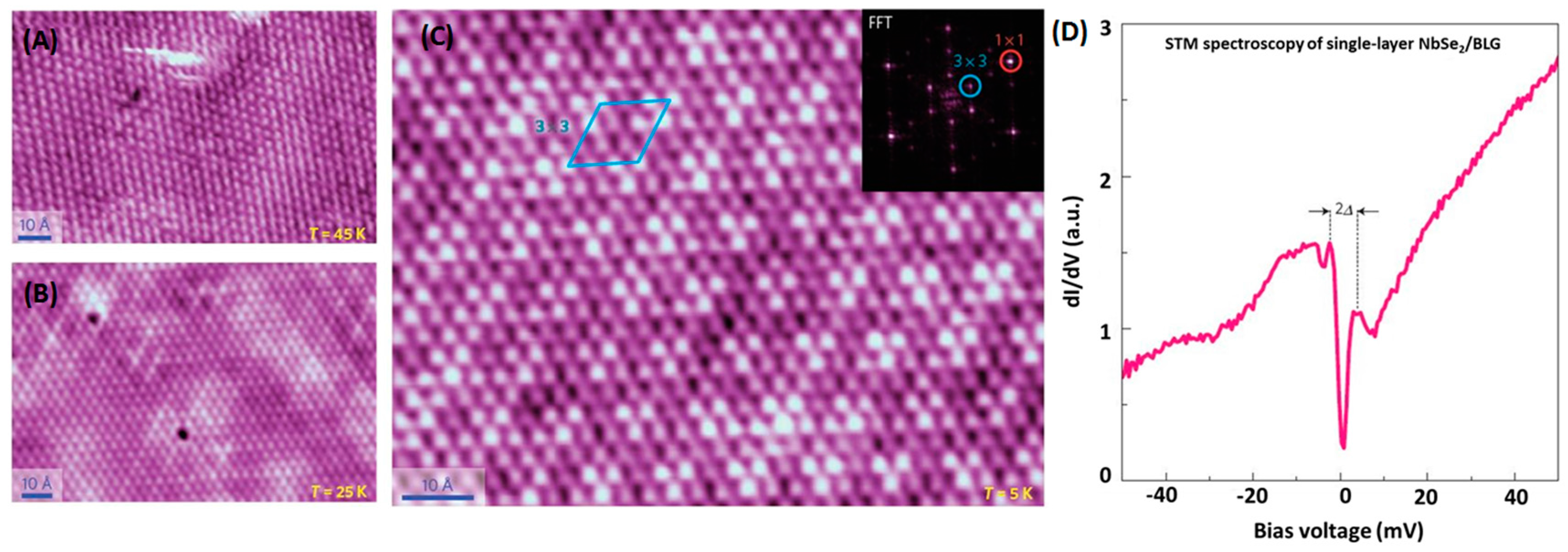
Atomic arrangement in 2D CDW materials regulates the electronic structures. STM imaging and scanning tunneling spectroscopy (STS) measurement are direct ways to reveal the atomic structure and the CDW energy gap of 2D CDW materials. M. M. Ugeda et al. reported STM measurements on ultrathin film of 2H-NbSe2 [68]. A 3 × 3 CDW structure in NbSe2 has been observed. Superconductivity also remains in the 2D limit, but the transition temperature is lowered to 1.9 K (7.2 K for the bulk material).
Figure 9A–C shows STM characterization for the NbSe2 monolayer (TCDW ∼ 35 K) in the temperature range from 45–5 K. At T = 45 K, the undistorted crystal structure is observed (Figure 9A). At T = 25 K, spotty and weak signatures of a superlattice become obvious (Figure 9B). The 3 × 3 CDW superlattice with the 1 × 1 atomic arrangement is developed fully and uniformly for the monolayer NbSe2 at 5 K (Figure 9C), which consists of the previously reported STM imaging of the bulk NbSe2 [20,89]. The low-bias dI/dV spectrum obtained for monolayer NbSe2 (Figure 9D) shows an energy gap feature centered at EF, possibly because of heterogeneity induced by the defects at the interface. The NbSe2 monolayer exhibits a keen sink at EF bounded by two narrow peaks that sit on top of an asymmetric background. The sink at EF does not reach all the way to zero, indicating that it is not a full gap in the electronic structure. STM measurements at 5 K reveal a CDW gap of ∆ = 4 meV at the Fermi energy, which is attainable by means of STM due to the shifting of bands crossing the Fermi level for a monolayer.
4. Applications of CDW Materials
4.1. Electrodes in Supercapacitors
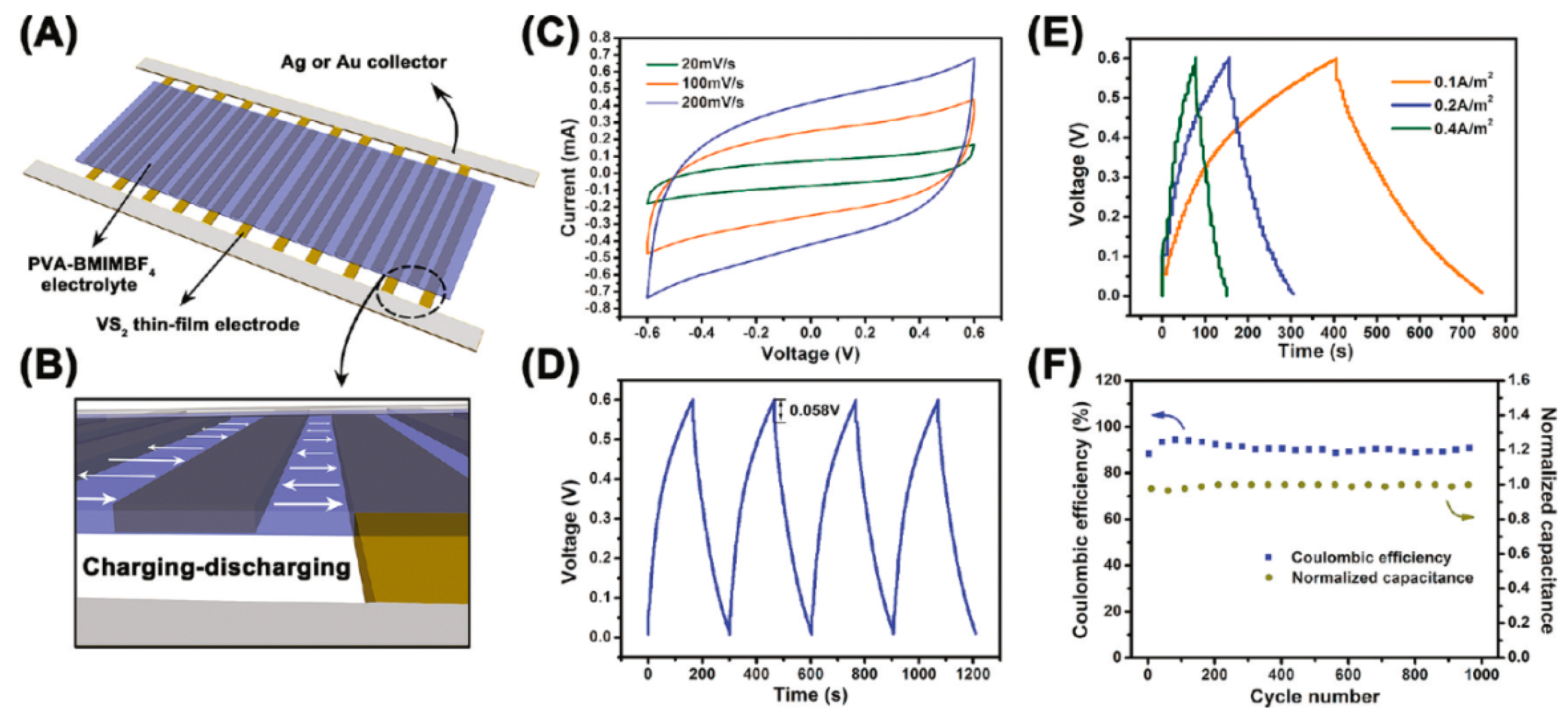
2D materials have provided new opportunities for ultrathin, transparent and flexible electronic devices. For supercapacitor application, conductivity and surface area are two demanding factors to evaluate the performance of supercapacitors [90]. Conventional inorganic graphene analogues (IGAs) are semiconducting or insulating with low conductivity, which hamper them from being employed as supercapacitor electrode materials [91,92]. In this aspect, thinner layers of 2D CDW materials could be a good choice. J. Feng et al. has reported using highly conductive ultrathin nanosheets of VS2 as the electrodes of in-plane supercapacitors [44] (see Figure 10), in which a high capacitance of 4760 μF/cm2 and an outstanding cycling lifetime (more than 1000 charge/discharge cycles) have been obtained.
4.2. Charge Density Wave-Based Oscillator
The CDW phase transition is associated with a lattice reconstruction, which results in much alteration of the material’s electrical properties. In the case of 1T-TaS2, when the applied electrical field is over 20 kV cm–1, the electrical conductivity instantly increases, which is ascribed to an insulator-to-metal transition (IMT) [93]. A contrary metal-to-insulator transition (MIT) is also observed when the voltage is swept back [93].
4.3. Photodetector
Photodetectors based on 2D heterojunctions have been studied extensively in recent years. 2H-NbSe2 crystals show a significant photoresponse at different wavelengths and intensity excitations. The photocurrent responsivity and photoconductive gain can reach 3.8 AW−1 and 300, respectively (Figure 12). The existence of electron trap states at the surface was responsible for the lower dark conductivity and expanded photoconductivity in the 2D 2H-NbSe2 nanostructures. This performance recognizes another prospect for utilization of 2D CDW materials as an optoelectronic component, as well as an ultrathin transparent conducting material.
4.4. Nonvolatile Memory
Semiconducting-based 2D TMDs and ferroelectric materials have been studied immensely to fabricate nonvolatile memory devices. Currently, the functionality of computer memory components is established on multi-stability, directed either by locally manipulating the density of electrons in the transistor or by changing the ferroelectric or magnetic order. A further possibility is switching between metallic and insulating phases by the ions’ motion. However, the speed is restricted by slow nucleation and diverse percolative growth. Recently, a 2D CDW material such as 1T-TaS2 has shown its potential to have the ultrafast current-driven nonvolatile switching, which showed the switching speed of 30 ps (Figure 13) [38]. L. Stojchevska et al. and M. Yoshida et al. also reported the photo-induced and current-driven nonvolatile memory function in the 1T-TaS2 thin flakes, respectively [39,94].
5. Sample Oxidation and Substrate Effect on CDW Transition
Bulk NbS2, NbSe2, TaS2 and TaSe2 are stable in air, but once cleaved to a few layers, then become highly air sensitive [1]. Oxygen (O2), water (H2O) and/or hydrocarbons can be adsorbed in the surface and react with the materials. Usually, by encapsulation with hexagonal boron nitride (h-BN) in an inert atmosphere, the intrinsic properties of atomically-thin crystals can be protected [37,88].
The substrate also plays a significant role in the fundamental properties of 2D materials. The choice of substrates can lead to distinct degrees of charge transfer and may also instigate mechanical instability, which leads to a change in carrier mobility and can be harmful for device processing [95]. Substrates can steer to modification of the band gap [96], along with indirect-to-direct band gap [97], modulation in the optical band gap and introduction of magnetism [98]. R. Zhao et al. reported tuning the phase transitions in 1T-TaS2 on different substrates [99], revealing that doping and charge transfer from the substrate have a minimal effect on CDW phase transitions, but substrate surface roughness is a predominant external factor on C-CDW transition temperature and hysteresis.
6. CDW Alloys
Two-dimensional CDW materials show a prosperous set of CDW orders, which typically coexist or compete with superconductivity. The mechanism of CDWs is still under controversy. There are a few reports that have proposed that the Fermi-surface nesting assists CDWs in the system [93,100,101,102,103,104], whereas some other studies have attributed this to the periodic-lattice-distortion structure [105,106]. Preparing a solid solution of various parent materials of the system and detecting the abnormality of the CDW properties may benefit understanding the CDW mechanism.
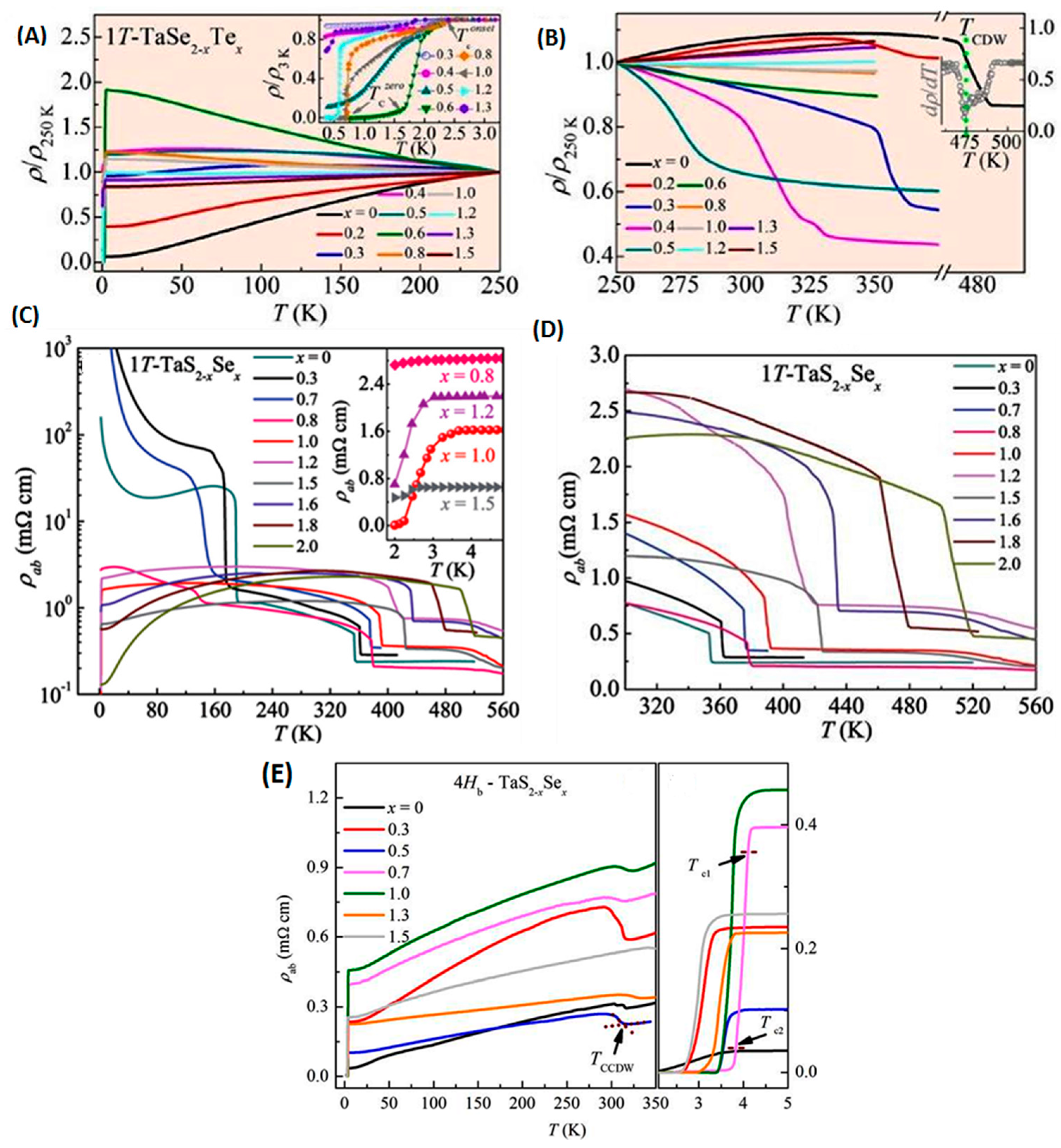
In recent years, some investigation have been performed on the CDW alloys like 4Hb-TaS2−X-SeX (0 ≤ X ≤ 2) [107], 1T-TaS2−XSeX (0 ≤ X ≤ 2) [33], 1T-TaSe2−XTeX (0 ≤ X ≤ 2) [108], 2H-NbSe2−XTeX (X = 0, 0.1, 0.2) [34], and 1T-FeXTa1–XS2 (0 ≤ X ≤ 0.05) [35] (see Figure 14). Recent study shows that superconductivity can be activated by Se-doping in layered charge density wave system 1T-TaS2–XSeX [33]. Coexistence of superconductivity and C-CDW in 4Hb-TaS2–X-SeX single crystals has been demonstrated lately [107]. Angle-resolved photoemission spectroscopy (ARPES) investigation on 1T-FeXTa1–XS2 (0 ≤ X ≤ 0.05) also denotes the direct experimental confirmation that superconductivity and NC-CDW coexist in real space [35]. Studies on 2H-TaS2 system are also widely analyzed by element doping [109]. For instance, Cu-intercalated single crystals of 2H-CuXTaS2 exhibit an outstanding enhancement of Tc from 0.8 K in 2H-TaS2 to 4.2 K in 2H-Cu0.03TaS2. It also suppresses the CDW transition to a low temperature [110].
Y. Liu et al. reported the nature of charge density waves and superconductivity in 1T-TaSe2−XTeX [108], which revealed that doping-activated disordered dispersion of Se/Te suppresses CDWs in 1T-TaSe2. The superconducting state with the highest Tc of 2.5 K was observed near CDWs. The superconducting volume is very little inside the CDW state and becomes substantial suddenly when the CDW state is completely suppressed.
7. Conclusions
Although there have been many publications on 2D CDW materials, the investigation on their properties and applications is still in its initial stage. The outstanding attributes of 2D CDW materials can offer enchanting new freedom for researchers to enhance the research activities in this rapidly expanding area. The prospective fields towards basic study are extensive including the advancement of new efficient approaches to prepare 2D crystals with a particular number of layers and upgrading the structural quality of the grown layers. The exploration of indispensable physicochemical characteristics of monolayer and few-layers crystals, strain effect, fabrication of interfacial attributes among the heterojunctions, the electric field and functionalization are all disclosed for expected research. In addition, the numerous opportunities of CDW materials and alloys with fascinating properties will make them an attainable material for future research that will help industries, as well as conclusively human beings.
Acknowledgments
We acknowledge the NSFC (Nos. 21373066 and 21673058), the Key Research Program of Frontier Sciences of CAS (QYZDB-SSW-SYS031), the Strategic Priority Research Program of CAS (XDA09040300), the Beijing Nova program (Z151100000315081) and the Beijing Talents Fund (2015000021223ZK17).
Author Contributions
Mongur Hossain and Liming Xie designed the project and wrote the manuscript. Juanxia Wu draw the crystal structures. Zhaoyang Zhao, Xinsheng Wang and Wen Wen assisted manuscript writing. All authors commented on the manuscript.
Conflicts of Interest
The authors declare no conflict of interest.
References
- Geim, A.K.; Grigorieva, I.V. Van der Waals heterostructures. Nature 2013, 499, 419–425. [Google Scholar] [CrossRef] [PubMed]
- Chhowalla, M.; Shin, H.S.; Eda, G.; Li, L.J.; Loh, K.P.; Zhang, H. The chemistry of two-dimensional layered transition metal dichalcogenide nanosheets. Nat. Chem. 2013, 5, 263–275. [Google Scholar] [CrossRef] [PubMed]
- Renteria, J.; Samnakay, R.; Jiang, C.; Pope, T.R.; Goli, P.; Yan, Z.; Wickramaratne, D.; Salguero, T.T.; Khitun, A.G.; Lake, R.K.; et al. All-metallic electrically-gated tantalum diselenide switches and logic circuits. J. Appl. Phys. 2014, 115, 034305. [Google Scholar] [CrossRef]
- Xu, K.; Chen, P.; Li, X.; Wu, C.; Guo, Y.; Zhao, J.; Wu, X.; Xie, Y. Ultrathin nanosheets of vanadium diselenide: a metallic two-dimensional material with ferromagnetic charge-density-wave behavior. Angew. Chem. Int. Ed. 2013, 52, 10477–10481. [Google Scholar] [CrossRef] [PubMed]
- Gomez, A.C.; Moratalla, E.N.; Guillermo, M.G.; Jorge, Q.J.; Cienfuegos, E.P.; Agraït, N.; Van der Zant, H.J.; Coronado, E.; Steele, G.A.; Bollinger, G.R. Fast and reliable identification of atomically thin layers of TaSe2 crystals. Nano Res. 2013, 6, 191–199. [Google Scholar] [CrossRef]
- Buscema, M.; Barkelid, M.; Zwiller, V.; Van der Zant, H.S.G.; Steele, G.A.; Castellanos, G.A. Large and tunable photothermoelectric effect in single-layer MoS2. Nano Lett. 2013, 13, 358–363. [Google Scholar] [CrossRef] [PubMed]
- Wickramaratne, D.; Zahid, F.; Lake, R.K. Electronic and thermoelectric properties of few-layer transition metal dichalcogenides. J. Chem. Phys. 2014, 140, 124710. [Google Scholar] [CrossRef] [PubMed] [Green Version]
- Renteria, J.; Samnakay, R.; Rumyantsev, S.L.; Jiang, C.; Goli, P.; Shur, M.S.; Balandin, A.A. Low-frequency 1/f Noise in molybdenum disulfide transistors. Appl. Phys. Lett. 2014, 104, 153104. [Google Scholar] [CrossRef]
- Taniguchi, K.; Matsumoto, A.; Shimotani, H.; Takagi, H. Electric-field-induced superconductivity at 9.4 K in a layered transition metal disulphide MoS2. Appl. Phys. Lett. 2012, 101, 042603. [Google Scholar] [CrossRef]
- Xi, X.; Zhao, L.; Wang, Z.; Berger, H.; Forró, L.; Shan, J.; Mak, K.F. Strongly enhanced charge-density-wave order in monolayer NbSe2. Nat. Nanotechnol. 2015, 10, 765–769. [Google Scholar] [CrossRef] [PubMed]
- Goli, P.; Khan, J.; Wickramaratne, D.; Lake, R.K.; Balandin, A.A. Charge density waves in exfoliated films of van der waals materials: Evolution of Raman spectrum in TiSe2. Nano Lett. 2012, 12, 5941–5945. [Google Scholar] [CrossRef] [PubMed]
- Gruner, G. The dynamics of charge-density waves. Rev. Mod. Phys. 1988, 60, 1129–1175. [Google Scholar] [CrossRef]
- Adelman, T.L.; Zaitsev-Zotov, S.V.; Thorne, R.E. Field-effect modulation of charge-density-wave transport in NbSe3 and TaS3. Phys. Rev. Lett. 1995, 74, 5264–5267. [Google Scholar] [CrossRef] [PubMed]
- Zaitsev-Zotov, S.V. Finite-size effects in quasi-one-dimensional conductors with a charge-density wave. Phys. Usp. 2004, 47, 533–553. [Google Scholar] [CrossRef]
- Moncton, D.E.; Axe, J.D.; DiSalvo, F.J. Study of superlattice formation in 2H-NbSe2 and 2H-TaSe2 by neutron Sscattering. Phys. Rev. Lett. 1975, 34, 734–737. [Google Scholar] [CrossRef]
- Fleming, R.M.; Schneemeyer, L.F.; Moncton, D.E. Commensurate-incommensurate transition in the charge-density-wave state of K0.30MoO3. Phys. Rev. B 1985, 31, 899–903. [Google Scholar] [CrossRef]
- Chu, C.W.; Testardi, L.R.; DiSalvo, F.J.; Moncton, D.E. Pressure effects on the charge-density-wave phases in 2H−TaSe2. Phys. Rev. B 1976, 14, 464–467. [Google Scholar] [CrossRef]
- Monney, C.; Battaglia, C.; Cercellier, H.; Aebi, P.; Beck, H. Exciton condensation driving the periodic lattice distortion of 1T−TiSe2. Phys. Rev. Lett. 2011, 106, 106404. [Google Scholar] [CrossRef] [PubMed]
- Bovet, M.; Popović, D.; Clerc, F.; Koitzsch, C.; Probst, U.; Bucher, E.; Berger, H.; Naumović, D.; Aebi, P. Pseudogapped Fermi surfaces of 1T-TaS2 and 1T-TaSe2: A charge density wave effect. Phys. Rev. B 2004, 69, 125117. [Google Scholar] [CrossRef]
- Arguello, C.J.; Chockalingam, S.P.; Rosenthal, E.P.; Zhao, L.; Gutiérrez, C.; Kang, J.H.; Chung, W.C.; Fernandes, R.M.; Jia, S.; Millis, A.J.; et al. Visualizing the charge density wave transition in 2H-NbSe2 in real space. Phys. Rev. B 2014, 89, 235115. [Google Scholar] [CrossRef]
- Mulazzi, M.; Chainani, A.; Katayama, N.; Eguchi, R.; Matsunami, M.; Ohashi, H.; Senba, Y.; Nohara, M.; Uchida, M.; Takagi, H.; et al. Absence of nesting in the charge-density-wave system 1T-VS2 as seen by photoelectron spectroscopy. Phys. Rev. B 2010, 82, 075130. [Google Scholar] [CrossRef]
- Tissen, V.G.; Osorio, M.R.; Brison, J.P.; Nemes, N.M.; Garcia-Hernandez, M.; Cario, L.; Rodiere, P.; Vieira, S.; Suderow, H. Pressure dependence of superconducting critical temperature and upper critical field of 2H-NbS2. Phys. Rev. B 2013, 87, 134502. [Google Scholar] [CrossRef]
- Dash, J.K.; Chen, L.; Dinolfo, P.H.; Lu, T.M.; Wang, G.C. A method toward fabricating semiconducting 3R-NbS2 ultrathin films. J. Phys. Chem. C 2015, 119, 19763–19771. [Google Scholar] [CrossRef]
- Valla, T.; Fedorov, A.V.; Johnson, P.D.; Glans, P.A.; McGuinness, C.; Smith, K.E.; Andrei, E.Y.; Berger, H. Quasiparticle spectra, charge-density waves, superconductivity, and electron-phonon coupling in 2H-NbSe2. Phys. Rev. Lett. 2004, 92, 086401. [Google Scholar] [CrossRef] [PubMed]
- Li, L.J.; Lu, W.J.; Liu, Y.; Qu, Z.; Ling, L.S.; Sun, Y.P. Influence of defects on charge-density-wave and superconductivity in 1T-TaS2 and 2H-TaS2 systems. Physica. C 2013, 492, 64–67. [Google Scholar] [CrossRef]
- Yu, Y.; Yang, F.; Lu, X.F.; Yan, Y.J.; Cho, Y.H.; Ma, L.; Niu, X.; Kim, S.; Son, Y.W.; Feng, D.; et al. Gate-tunable phase transitions in thin flakes of 1T-TaS2. Nat. Naotechnol. 2015, 10, 270–276. [Google Scholar] [CrossRef] [PubMed]
- Cao, Y.F.; Cai, K.M.; Li, L.J.; Lu, W.J.; Sun, Y.P.; Wang, K.Y. Transport and capacitance properties of charge density wave in few layer 2H-TaS2 devices. Chin. Phys. Lett. 2014, 31, 077203. [Google Scholar] [CrossRef]
- Samnakay, R.; Wickramaratne, D.; Pope, R.; Lake, R.K.; Salguero, T.T.; Balandin, A.A. Zone-folded phonons and the commensurate incommensurate charge-density-wave transition in 1T-TaSe2 thin films. Nano Lett. 2015, 15, 2965–2973. [Google Scholar] [CrossRef] [PubMed]
- Luo, H.X.; Xie, W.W.; Tao, J.; Inoue, H.; Gyenis, A.; Krizan, J.W.; Yazdani, A.; Zhu, Y.M.; Cava, R.J. Polytypism, polymorphism, and superconductivity in TaSe2−XTeX. Proc. Natl. Acad. Sci. USA 2015, 112, E1174–E1180. [Google Scholar] [CrossRef] [PubMed]
- Dardel, B.; Grioni, M.; Malterre, D.; Weibel, P.; Baer, Y.; Levy, F. Spectroscopic observation of charge-density-wave-induced changes in the electronic structure of 2H-TaSe2. J. Phys. Condens. Matter 1993, 5, 6111–6120. [Google Scholar] [CrossRef]
- Hajiyev, P.; Cong, C.; Qiu, C.; Yu, T. Contrast and Raman spectroscopy study of single- and few-layered charge density wave material: 2H-TaSe2. Sci. Rep. 2013, 3, 2593. [Google Scholar] [CrossRef] [PubMed]
- Morosan, E.; Zandbergen, H.W.; Dennis, B.S.; Bos, J.W.G.; Onose, Y.; Klimczuk, T.; Ramirez, A.P.; Ong, N.P.; Cava, R.J. Superconductivity in CuXTiSe2. Nat. Phys. 2006, 2, 544. [Google Scholar] [CrossRef]
- Liu, Y.; Ang, R.; Lu, W.J.; Song, W.H.; Li, L.J.; Sun, Y.P. Superconductivity induced by Se-doping in layered charge-density-wave system 1T-TaS2–XSeX. Appl. Phys. Lett. 2013, 102, 192602. [Google Scholar] [CrossRef]
- Tao, W.H.; Jun, L.L.; Shu, Y.D.; Hong, C.X.; An, X.Z. Effect of Te doping on superconductivity and charge-density wave in dichalcogenides 2H-NbSe2-XTeX (X = 0, 0.1, 0.2). Chin. Phys. Soc. 2007, 16, 2471–2474. [Google Scholar]
- Ang, R.; Tanaka, Y.; Ieki, E.; Nakayama, K.; Sato, T.; Li, L.J.; Lu, W.J.; Sun, Y.P.; Takahashi, T. Real-space coexistence of the melted mott state and superconductivity in Fe-substituted 1T−TaS2. Phys. Rev. Lett. 2012, 109, 176403. [Google Scholar] [CrossRef] [PubMed]
- Kusmartseva, A.F.; Sipos, B.; Berger, H.; Forro, L.; Tutis, E. Pressure induced superconductivity in pristine 1T-TiSe2. Phys. Rev. Lett. 2009, 103, 236401. [Google Scholar] [CrossRef] [PubMed]
- Liu, G.; Debnath, B.; Pope, T.R.; Salguero, T.T.; Lake, R.K.; Balandin, A.A. A charge-density-wave oscillator based on an integrated tantalum disulfide–boron nitride–graphene device operating at room temperature. Nat. Nanotechnol. 2016, 11, 845–850. [Google Scholar] [CrossRef] [PubMed]
- Vaskivskyi, I.; Mihailovic, I.A.; Brazovskii, S.; Gospodaric, J.; Mertelj, T.; Svetin, D.; Sutar, P.; Mihailovic, D. Fast electronic resistance switching involving hidden charge density wave states. Nat. Commun. 2016, 7, 11442. [Google Scholar] [CrossRef] [PubMed]
- Stojchevska, L.; Vaskivskyi, I.; Mertelj, T.; Kusar, P.; Svetin, D.; Brazovskii, S.; Mihailovic, D. Ultrafast switching to a stable hidden quantum state in an electronic crystal. Science 2014, 344, 177–180. [Google Scholar] [CrossRef] [PubMed]
- Frindt, R.F. Superconductivity in Ultrathin NbSe2 Layers. Phys. Rev. Lett. 1972, 26, 299–301. [Google Scholar] [CrossRef]
- Moratalla, E.N.; Island, J.O.; Valero, S.M.; Cienfuegos, E.P.; Gomez, A.C.; Quereda, J.; Bollinger, G.R.; Chirolli, L.; Guillén, J.A.S.; Agraït, N.; et al. Enhanced superconductivity in atomically thin TaS2. Nat. Commun. 2016, 7, 11043. [Google Scholar] [CrossRef] [PubMed]
- Li, H.; Lu, G.; Wang, Y.; Yin, Z.; Cong, C.; He, Q.; Wang, L.; Ding, F.; Yu, T.; Hua, Z. Mechanical exfoliation and characterization of single- and few-layer nanosheets of WSe2, TaS2, and TaSe2. Small 2013, 9, 1974–1981. [Google Scholar] [CrossRef] [PubMed]
- El-Bana, M.S.; Wolverson, D.; Russo, S.; Balakrishnan, G.; Paul, D.M.; Simon, J.B. Superconductivity in two-dimensional NbSe2 field effect transistors. Supercond. Sci. Technol. 2013, 26, 125020. [Google Scholar] [CrossRef]
- Feng, J.; Sun, X.; Wu, C.; Peng, L.; Lin, C.; Hu, S.; Yang, J.; Xie, Y. Metallic few-layered VS2 ultrathin nanosheets: High two-dimensional conductivity for in-plane supercapacitors. J. Am. Chem. Soc. 2011, 133, 17832–17838. [Google Scholar] [CrossRef] [PubMed]
- Zeng, Z.; Tan, C.; Huang, X.; Bao, S.; Zhang, H. Growth of noble metal nanoparticles on single layer TiS2 and TaS2 nanosheets for hydrogen evolution reaction. Energy Environ. Sci. 2014, 7, 797–803. [Google Scholar] [CrossRef]
- Coleman, J.N.; Lotya, M.; O’Neill, A.; Bergin, S.D.; King, P.J.; Khan, U.; Young, K.; Gaucher, A.; De, S.; Smith, R.J.; et al. Two-Dimensional nanosheets produced by liquid exfoliation of layered materials. Science 2011, 331, 568–571. [Google Scholar] [CrossRef] [PubMed]
- Shiogai, J.; Ito, Y.; Mitsuhashi, T.; Nojima, T.; Tsukazaki, A. Electric-field-induced superconductivity in electrochemically etched ultrathin FeSe films on SrTiO3 and MgO. Nat. Phys. 2016, 12, 42–46. [Google Scholar] [CrossRef]
- Yoshida, M.; Ye, J.; Terukazu, N.; Norio, K.; Yoshihiro, I. Electrostatic and electrochemical tuning of superconductivity in two-dimensional NbSe2 crystals. App. Phys. Lett. 2016, 108, 202602. [Google Scholar] [CrossRef]
- Le’vy, F. Crystallography and Crystal Chemistry of Materials with Layered Structure; D. Reidel Publishing Company: Dordrecht, The Netherlands, 1976; Volume 2. [Google Scholar]
- Yang, J.; Wang, W.; Liu, Y.; Du, H.; Ning, W.; Zheng, G.; Jin, C.; Han, Y.; Wang, N.; Yang, Z.; et al. Thickness dependence of the charge-density-wave transition temperature in VSe2. Appl. Phys. Lett. 2014, 105, 063109. [Google Scholar] [CrossRef]
- Yan, Z.; Jiang, C.; Pope, T.R.; Tsang, C.F.; Stickney, J.L.; Goli, P.; Renteria, J.; Salguero, T.T.; Balandin, A.A. Phonon and thermal properties of exfoliated TaSe2 thin films. J. Appl. Phys. 2013, 114, 204301. [Google Scholar] [CrossRef]
- Huang, Y.H.; Chen, R.S.; Zhang, J.R.; Huang, Y.S. Electronic transport in NbSe2 two-dimensional nanostructures: Semiconducting characteristics and photoconductivity. Nanoscale 2015, 7, 18964–18970. [Google Scholar] [CrossRef] [PubMed]
- Wang, J.; Zheng, H.; Xu, G.; Sun, L.; Hu, D.; Lu, L.; Liu, L.; Zheng, J.; Tao, C.; Jiao, L. Controlled synthesis of two-dimensional 1T-TiSe2 with charge density wave transition by chemical vapor transport. J. Am. Chem. Soc. 2016, 138, 16216–16219. [Google Scholar] [CrossRef] [PubMed]
- Choy, K.L. Chemical vapour deposition of coatings. Prog. Mater. Sci. 2003, 48, 57–170. [Google Scholar] [CrossRef]
- Hou, X.; Choy, K.L. Processing and applications of aerosol-assisted chemical vapor deposition. Chem. Vap. Deposition 2006, 12, 583–596. [Google Scholar] [CrossRef]
- Yuan, J.; Wu, J.; Hardy, W.J.; Loya, P.; Lou, M.; Yang, Y.; Najmaei, S.; Jiang, M.; Qin, F.; Keyshar, K.; et al. Facile synthesis of single crystal vanadium disulfide nanosheets by chemical vapor deposition for efficient hydrogen evolution reaction. Adv. Mater. 2015, 27, 5605–5609. [Google Scholar] [CrossRef] [PubMed]
- Ji, Q.; Li, C.; Wang, J.; Niu, J.; Gong, Y.; Zhang, Z.; Fang, Q.; Zhang, Y.; Shi, J.; Liao, L.; et al. Metallic vanadium disulfide nanosheets as a platform material for multifunctional electrode applications. Nano Lett. 2017, 17, 4908–4916. [Google Scholar] [CrossRef] [PubMed]
- Nicolas, D.B.; Christopher, S.B.; Claire, J.C.; Ivan, P.P.; Prieto, A.G. Atmospheric pressure chemical vapour deposition of vanadium diselenide thin films. App. Surf. Sci. 2007, 253, 6041–6046. [Google Scholar]
- Zhang, Z.; Niu, J.; Yang, P.; Gong, Y.; Ji, Q.; Shi, J.; Fang, Q.; Jiang, S.; Li, H.; Zhou, X. Van der waals epitaxial growth of 2D metallic vanadium diselenide single crystals and their extra-high electrical conductivity. Adv. Mater. 2017, 1702359. [Google Scholar] [CrossRef] [PubMed]
- Wang, X.; Lin, J.; Zhu, Y.; Luo, C.; Suenaga, K.; Cai, C.; Xie, L. Chemical vapor deposition of trigonal prismatic NbS2 monolayer and 3R-polytype few-Layers. Nanoscale 2017. in revision. [Google Scholar]
- Wang, H.; Huang, X.; Lin, J.; Cui, J.; Chen, Y.; Zhu, C.; Liu, F.; Zeng, Q.; Zhou, J.; Yu, P.; et al. High-quality monolayer superconductor NbSe2 grown by chemical vapour deposition. Nat. Commun. 2017, 8, 394. [Google Scholar] [CrossRef] [PubMed]
- Fu, W.; Chen, Y.; Lin, J.; Wang, X.; Zheng, Q.; Zhou, J.; Zheng, L.; Wang, H.; He, Y.; Fu, Q.; et al. Controlled synthesis of atomically thin 1T-TaS2 for tunable charge density wave phase transitions. Chem. Mater. 2016, 28, 7613–7618. [Google Scholar] [CrossRef]
- Jin, G.; Kim, C.; Jo, H.; Kwon, S.H.; Jeong, S.J.; Lee, H.B.R.; Ahn, J.H. Vapor phase synthesis of TaS2 nanocrystals with iodine as transport agent. Jpn. J. Appl. Phys. 2017, 56, 045501. [Google Scholar] [CrossRef]
- Boscher, N.D.; Carmalt, C.J.; Parkin, I.P. Atmospheric pressure CVD of TiSe2 thin films on glass. Chem. Vap. Deposition 2006, 12, 54–58. [Google Scholar] [CrossRef]
- Bae, S.; Kim, H.; Lee, Y.; Xu, X.; Park, J.S.; Zheng, Y.; Balakrishnan, J.; Lei, T.; Kim, H.R.; Song, Y.I.; et al. Roll-to-roll production of 30-inch graphene films for transparent electrodes. Nat. Nanotechnol. 2010, 5, 574–578. [Google Scholar] [CrossRef] [PubMed]
- Jun, P.P.; Guan, J.Q.; Zhang, H.M.; Song, C.L.; Wang, L.; He, K.; Xue, Q.K.; Ma, X.C. Molecular beam epitaxy growth and scanning tunneling microscopy study of TiSe2 ultrathin films. Phys. Rev. B 2015, 91, 12113. [Google Scholar]
- Nishikawa, H.; Shimada, T.; Koma, A. Epitaxial growth of TiSe2 thin films on Se-terminated GaAs(111)B. J. Vacuu. Sci. Tech. A 1996, 14, 2893. [Google Scholar] [CrossRef]
- Ugeda, M.M.; Bradley, A.J.; Zhang, Y.; Onishi1, S.; Chen, Y.; Ruan, W.; Aristizaba, C.O.; Ryu, H.; Mark, T.; Edmonds, M.T.; et al. Characterization of collective ground states in single-layer NbSe2. Nat. Phys. 2016, 12, 92–97. [Google Scholar] [CrossRef]
- Koma, A.; Sunouchi, K.; Miyajima, T. Electronic structure of a monolayer NbSe2 film grown heteroepitaxially on the cleaved face of 2H-MoS2. In Proceedings of the 17th International Conference on the Physics of Semiconductors, San Francisco, CA, USA, 6–10 August 1984; pp. 1465–1468. [Google Scholar]
- Shimada, T.; Ohuchi, F.S.; Koma, A. Polytypes and charge-density waves of ultrathin TaS2 films grown by van der Waals epitaxy. Surf. Sci. 1993, 291, 57–66. [Google Scholar] [CrossRef]
- Sugai, S.; Murase, K.; Uchida, S.; Tanaka, S. Investigation of the charge density waves in 1T-VSe2 by Raman scattering. J. Phy. Colloques. 1981, 42, 740–742. [Google Scholar]
- Hirata, T.; Ohuchi, F.S. Temperature dependence of the Raman spectra of 1T-TaS2. Solid State Communs. 2001, 117, 361–364. [Google Scholar] [CrossRef]
- Sugai, S.; Murase, K. Generelized electronic susceptibility and charge density waves in 2H-TaSe2 by Raman scattering. Phys. Rev. B. 1982, 25, 2418–2427. [Google Scholar] [CrossRef]
- Cong, C.; Yu, T.; Sato, K.; Shang, J.; Saito, R.; Dresselhaus, G.F.; Dresselhaus, M.S. Raman characterization of ABA-and-ABC-Stacked trilayer graphene. ACS Nano. 2011, 5, 8760–8768. [Google Scholar] [CrossRef] [PubMed]
- Lui, C.H.; Li, Z.; Chen, Z.; Klimov, P.V.; Brus, L.E.; Heinz, T.F. Imaging stacking order in few-layer graphene. Nano lett. 2011, 11, 164–169. [Google Scholar] [CrossRef] [PubMed]
- Li, S.L.; Miyazaki, H.; Song, H.; Kuramochi, H.; Nakaharai, S.; Tsukagoshi, K. Quantitative Raman spectrum and reliable thickness identification for atomic layers on insulating substrates. ACS Nano. 2012, 6, 7381–7388. [Google Scholar] [CrossRef] [PubMed]
- Lv, R.; Li, Q.; Méndez, A.R.B.; Hayashi, T.; Wang, B.; Berkdemir, A.; Hao, Q.; Elías, A.L.; Silva, R.S.; Gutiérrez, H.R.; et al. Nitrogen-doped graphene: Beyond single substitution and enhanced molecular sensing. Sci. Rep. 2012, 2, 586. [Google Scholar] [CrossRef] [PubMed]
- Cong, C.; Li, K.; Zhang, X.X.; Yu, T. Visualization of arrangements of carbon atoms in graphene layers by Raman mapping and atomic-resolution TEM. Sci. Rep. 2013, 3, 1195. [Google Scholar] [CrossRef] [PubMed]
- Cong, C.; Yu, T.; Wang, H.M. Raman study on the G mode of graphene for determination of edge orientation. ACS Nano. 2010, 4, 3175–3180. [Google Scholar] [CrossRef] [PubMed]
- Lee, J.E.; Ahn, G.; Shim, J.; Lee, Y.S.; Ryu, S. Optical separation of mechanical strain from charge doping in graphene. Nat. Communs. 2012, 3, 1024. [Google Scholar] [CrossRef] [PubMed]
- Ni, Z.H.; Yu, T.; Lu, Y.H.; Wang, Y.Y.; Feng, Y.P.; Shen, Z.X. Uniaxial strain on graphene: Raman spectroscoy study and bandgap opening. ACS Nano. 2008, 2, 2301–2305. [Google Scholar] [CrossRef] [PubMed]
- Wilson, J.A.; Di Salvo, F.J.; Mahajan, S. Charge-density waves in metallic, layered, transition-metal dichalcogenides. Phys. Rev. Lett. 1974, 32, 882–884. [Google Scholar] [CrossRef]
- Rossnagel, K. On the origin of charge-density waves in select layered transitionmetal dichalcogenides. J. Phys. Condens. Matter 2011, 23, 213001. [Google Scholar] [CrossRef] [PubMed]
- Maclean, D.; Jericho, M.H. Effect of the charge-density-wave transition on the thermal expansion of 2H-TaSe2, NbSe3, and o-TaS3. Phys. Rev. B 1993, 47, 16169–16177. [Google Scholar] [CrossRef]
- Tada, H.; Kumpel, A.E.; Lathrop, R.E.; Slanina, J.B. Thermal expansion coefficient of polycrystalline silicon and silicon dioxide thin films at high temperatures. App. Phy. Lett. 2000, 87, 61–68. [Google Scholar] [CrossRef]
- Mutka, H.; Zuppiroli, L.; Molinie, P.; Bourgoin, J.C. Charge-density waves and localization in electron-irradiated 1T−TaS2. Phys. Rev. B 1981, 23, 5030–5037. [Google Scholar] [CrossRef]
- Yoshida, M.; Yijin, Z.; Jianting, Y.; Ryuji, S.; Yasuhiko, I.; Shigeru, K.; Akihiko, F.; Yoshihiro, I. Controlling charge-density-wave states in nano-thick crystals of 1T-TaS2. Sci. Rep. 2014, 4, 7302. [Google Scholar] [CrossRef] [PubMed]
- Tsen, A.W.; Hovden, R.; Wang, D.; Kim, Y.D.; Okamoto, J.; Spoth, K.A.; Liu, Y.; Lu, W.; Sunf, Y.; James, C.; et al. Structure and control of charge density waves in two-dimensional 1T-TaS2. Proc. Natl. Acad. Sci. USA. 2015, 112, 15054–15059. [Google Scholar] [CrossRef] [PubMed]
- Giambattista, B.; Johnson, A.; Coleman, R.V.; Drake, B.; Hansma, P.K. Charge-density waves observed at 4.2 K by scanning-tunneling microscopy. Phys. Rev. B 1988, 37, 2741–2744. [Google Scholar] [CrossRef]
- Zhu, Y.; Murali, S.; Stoller, M.D.; Ganesh, K.J.; Cai, W.; Ferreira, P.J.; Pirkle, A.; Wallace, R.R.; Cychosz, K.A.; Thommes, M.; et al. Carbon-based supercapacitors produced by activation of graphene. Science 2011, 332, 1537–1541. [Google Scholar] [CrossRef] [PubMed]
- Rao, C.N.R.; Nag, A. Inorganic Analogues of Graphene. Eur. J. Inorg. Chem. 2010, 27, 4244–4250. [Google Scholar] [CrossRef]
- Nag, A.; Raidongia, K.; Hembram, K.P.S.S.; Datta, R.; Waghmare, U.V.; Rao, C.N.R. Graphene analogues of BN: Novel synthesis and properties. ACS Nano. 2010, 4, 1539–1544. [Google Scholar] [CrossRef] [PubMed]
- Myron, H.W.; Rath, J.; Freeman, A.J. Generalized electronic susceptibility and charge-density waves in 1T−TaS2 and 1T−TaSe2. Phys. Rev. B 1977, 15, 885–889. [Google Scholar] [CrossRef]
- Yoshida, M.; Suzuki, R.; Zhang, Y.; Nakano, M.; Iwasa, Y. Memristive phase switching in two-dimensional 1T-TaS2 crystals. Sci. Adv. 2015, 1, 1–6. [Google Scholar] [CrossRef] [PubMed]
- Neto, H.C.; Novoselov, K. New directions in science and technology: Two-dimensional crystals. Rep. Prog. Phys. 2011, 74, 082501. [Google Scholar] [CrossRef]
- Castellanos, G.A.; Roldán, R.; Cappelluti, E.; Buscema, M.; Guinea, F.; van der Zant, H.S.J.; Steele, G.A. Local strain engineering in atomically thin MoS2. Nano Lett. 2013, 13, 5361–5366. [Google Scholar] [CrossRef] [PubMed]
- Desai, S.B.; Seol, G.; Kang, J.S.; Fang, H.; Battaglia, C.; Kapadia, R.; Ager, J.W.; Guo, J.; Javey, A. Strain-induced indirect to direct bandgap transition in multi-layer WSe2. Nano Lett. 2014, 14, 4592–4597. [Google Scholar] [CrossRef] [PubMed]
- Yang, S.; Wang, C.; Sahin, H.; Chen, H.; Li, Y.; Li, S.S.; Suslu, A.; Peeters, F.M.; Liu, Q.; Li, J.; et al. Tuning the optical, magnetic, and electrical properties of ReSe2 by nanoscale strain engineering. Nano Lett. 2015, 15, 1660. [Google Scholar] [CrossRef] [PubMed]
- Zhao, R.; Wang, Y.; Deng, D.; Luo, X.; Lu, W.J.; Sun, Y.P.; Liu, Z.K.; Chen, L.Q.; Robinson, J. Tuning phase transitions in 1T-TaS2 via the substrate. Nano Lett. 2017, 17, 3471–3477. [Google Scholar] [CrossRef] [PubMed]
- Tanda, S.; Sambongi, T.; Tani, T.; Tanaka, S. X-Ray Study of Charge Density Wave Structure in 1T-TaS2. J. Phys. Soc. Jpn. 1984, 53, 476–479. [Google Scholar] [CrossRef]
- Myron, H.W.; Freeman, A.J. Electronic structure and Fermi-surface-related instabilities in 1T-TaS2 and 1T-TaSe2. Phys. Rev. B 1975, 11, 2735–2739. [Google Scholar] [CrossRef]
- Wilson, J.A.; Di Salvo, F.J.; Mahajan, S. Charge-density waves and superlattices in the metallic layered transition metal dichalcogenides. Adv. Phys. 1975, 24, 117–201. [Google Scholar] [CrossRef]
- Battaglia, C.; Cercellier, H.; Clerc, F.; Despont, L.; Garnier, L.M.G.; Koitzsch, C.; Aebi, P.; Berger, H.; Forr´o, L.; Draxl, C.A. Fermi-surface-induced lattice distortion in NbTe2. Phys. Rev. B 2005, 72, 195114. [Google Scholar] [CrossRef]
- Sharma, S.; Nordstrom, L.; Johansson, B. Stabilization of charge-density waves inm 1T-TaX2 (X = S, Se, Te): First-principles total energy calculations. Phys. Rev. B 2002, 66, 195101. [Google Scholar] [CrossRef]
- Liu, A.Y. Electron-phonon coupling in compressed 1T-TaS2: Stability and superconductivity from first principles. Phys. Rev. B 2009, 79, 220515. [Google Scholar]
- Ge, Y.; Liu, A.Y. First-principles investigation of the charge-density-wave instability in 1T-TaSe2. Phys. Rev. B 2010, 82, 155133. [Google Scholar] [CrossRef]
- Liu, Y.; Li, L.J.; Lu, W.J.; Ang, R.; Liu, X.Z.; Sun, Y.P. Coexistence of superconductivity and commensurate charge density wave in 4Hb-TaS2–XSeX single crystals. J. Appl. Phys. 2014, 115, 043915. [Google Scholar] [CrossRef]
- Liu, Y.; Shao, D.F.; Li, L.J.; Lu, W.J.; Zhu, X.D.; Tong, P.; Xiao, R.C.; Ling, L.S.; Xi, C.Y.; Pi, L.; et al. Nature of charge density waves and superconductivity in 1T-TaSe2−XTeX. Phys. Rev. B 2016, 94, 045131. [Google Scholar] [CrossRef]
- Li, L.J.; Zhu, X.D.; Sun, Y.P.; Lei, H.C.; Wang, B.S.; Zhang, S.B.; Zhu, X.B.; Yang, Z.R.; Song, W.H. Superconductivity of Ni-doping 2H-TaS2. Physica. C 2010, 470, 313–317. [Google Scholar] [CrossRef]
- Zhu, X.D.; Sun, Y.P.; Zhu, X.B.; Luo, X.; Wang, B.S.; Li, G.; Yang, Z.R.; Song, W.H.; Dai, J.M. Single crystal growth and characterizations of Cu0.03TaS2 superconductors. J. Cryst. Growth 2008, 311, 218–221. [Google Scholar] [CrossRef]
Figure 1.
Illustration of transition from the normal state to the charge-density-wave state in one dimension. The atomic displacements lead to the formation of a “superlattice’’ resulting in opening of an electronic energy band gap.
Figure 1.
Illustration of transition from the normal state to the charge-density-wave state in one dimension. The atomic displacements lead to the formation of a “superlattice’’ resulting in opening of an electronic energy band gap.

Figure 2.
Schematics of structural polytypes of 2D charge density wave (CDW) materials: 1T (tetragonal symmetry), 2H (hexagonal symmetry) and 3R (rhombohedral symmetry).
Figure 2.
Schematics of structural polytypes of 2D charge density wave (CDW) materials: 1T (tetragonal symmetry), 2H (hexagonal symmetry) and 3R (rhombohedral symmetry).
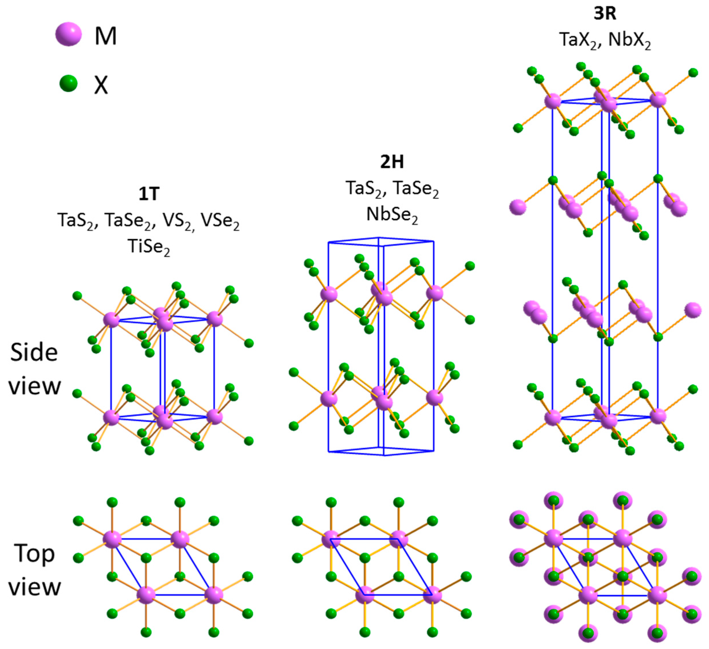
Figure 3.
Optical images of mechanically-exfoliated 2H-TaSe2 (A,B). (C) White light contrast spectra of the 2H-TaSe2 monolayer and a few layers. Data are reproduced from [31]. Copyright © 2013, Nature Publishing Group.
Figure 3.
Optical images of mechanically-exfoliated 2H-TaSe2 (A,B). (C) White light contrast spectra of the 2H-TaSe2 monolayer and a few layers. Data are reproduced from [31]. Copyright © 2013, Nature Publishing Group.

Figure 4.
Synthesis of ultrathin VS2 nanosheets by the liquid exfoliation method. (A) VS2·NH3 precursor with NH3 molecules intercalated into the S-V-S layers. (B) Diffusion of NH3 molecules apart from the stacked layers, breaking down the c axis periodicity and resulting in the formation of ultrathin VS2 nanosheets. (C) Vacuum-filtration assembly of the as-synthesized VS2 nanosheets into thin films on mixed cellulose membrane. (D,E) SEM and AFM image of as-synthesized VS2 nanosheets, respectively. Data are reproduced with permission from [44]. Copyright (2011) American Chemical Society.
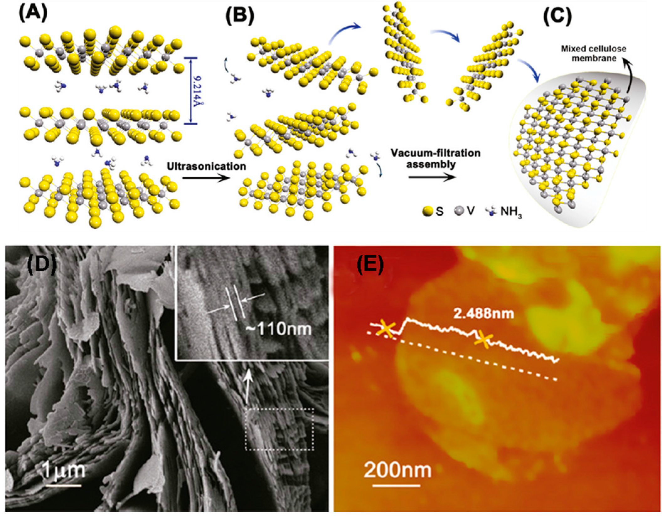
Figure 5.
Synthesis of 1T-TiSe2 flakes using the chemical vapor transport (CVT) method. (A) Schematic for the setup of the surface growth of 2D TiSe2. (B,C) Optical and AFM images of the as-grown TiSe2 flakes on the C-plane sapphire substrate, respectively. Data are reproduced with permission from [53]. Copyright (2016) American Chemical Society.

Figure 6.
(A) Illustration of CVD growth of 1T-TaS2 crystals using TaCl5 and S as precursors. (B–D) Optical images of the as-prepared 1T-TaS2 crystals of different thicknesses. Data are reproduced with permission from [62]. Copyright (2016) American Chemical Society.
Figure 6.
(A) Illustration of CVD growth of 1T-TaS2 crystals using TaCl5 and S as precursors. (B–D) Optical images of the as-prepared 1T-TaS2 crystals of different thicknesses. Data are reproduced with permission from [62]. Copyright (2016) American Chemical Society.
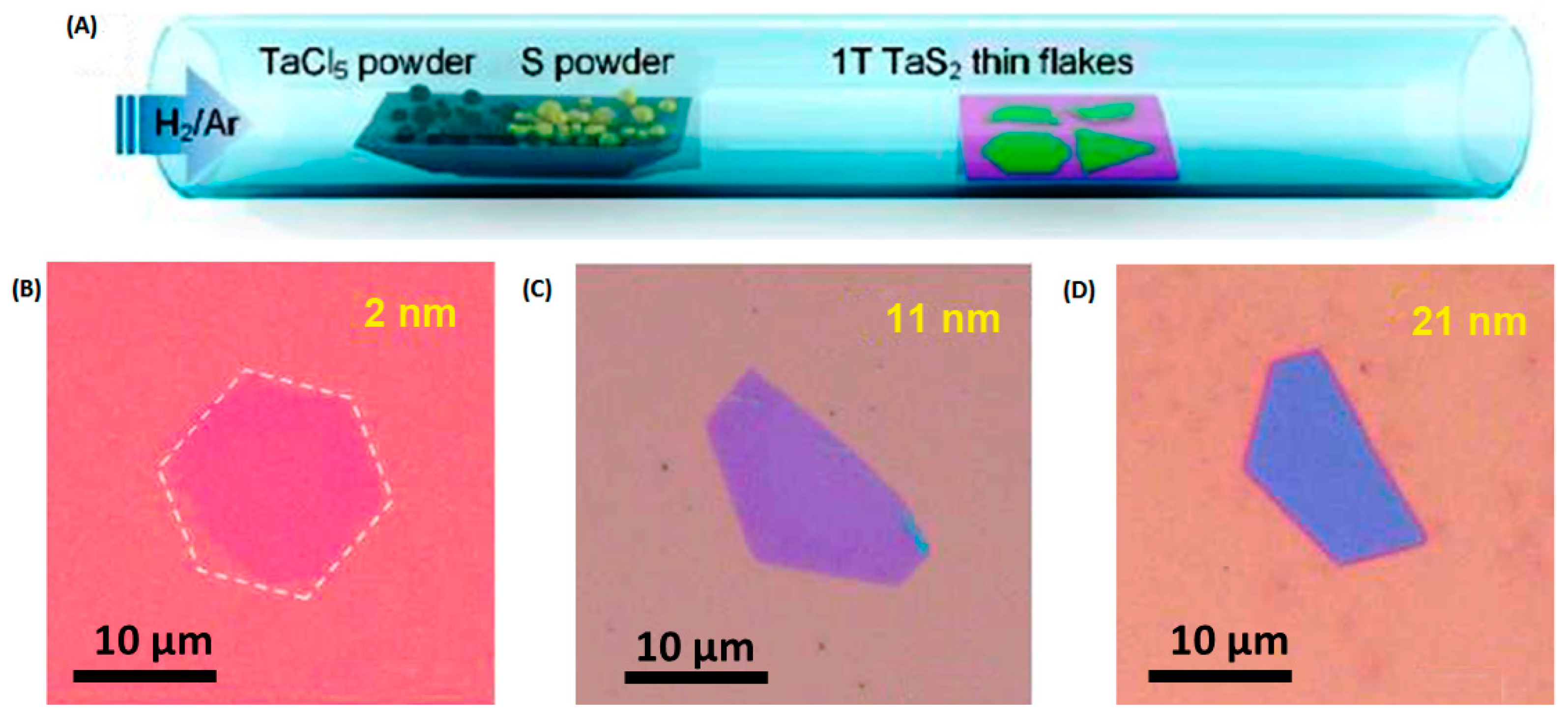
Figure 7.
(A,B) Temperature-dependent Raman spectrum of the thick (150 nm) and thin (35 nm) sample of 1T-TaSe2 in the heating cycle from 213–493 K, respectively. (C) Low temperature Raman spectrum of the double layer 2H-TaSe2 sample. (D) Sudden softening of two-phonon (E1g) peaks of 2H-TaSe2. Data are reproduced with permission from: 1T-TaSe2 [28], Copyright (2015) American Chemical Society; 2H-TaSe2 [31], Copyright © 2013, Nature Publishing Group.

Figure 8.
Temperature-dependent electrical property. (A,B) Temperature-dependent electrical resistivity of 1T-TaS2 and 1T-VSe2 in varying of thicknesses, respectively. Data are reproduced with permission from: 1T-VSe2 [50], Copyright (2014) AIP Publishing LLC; 1T-TaS2 [26], Copyright © 2015, Nature Publishing Group.
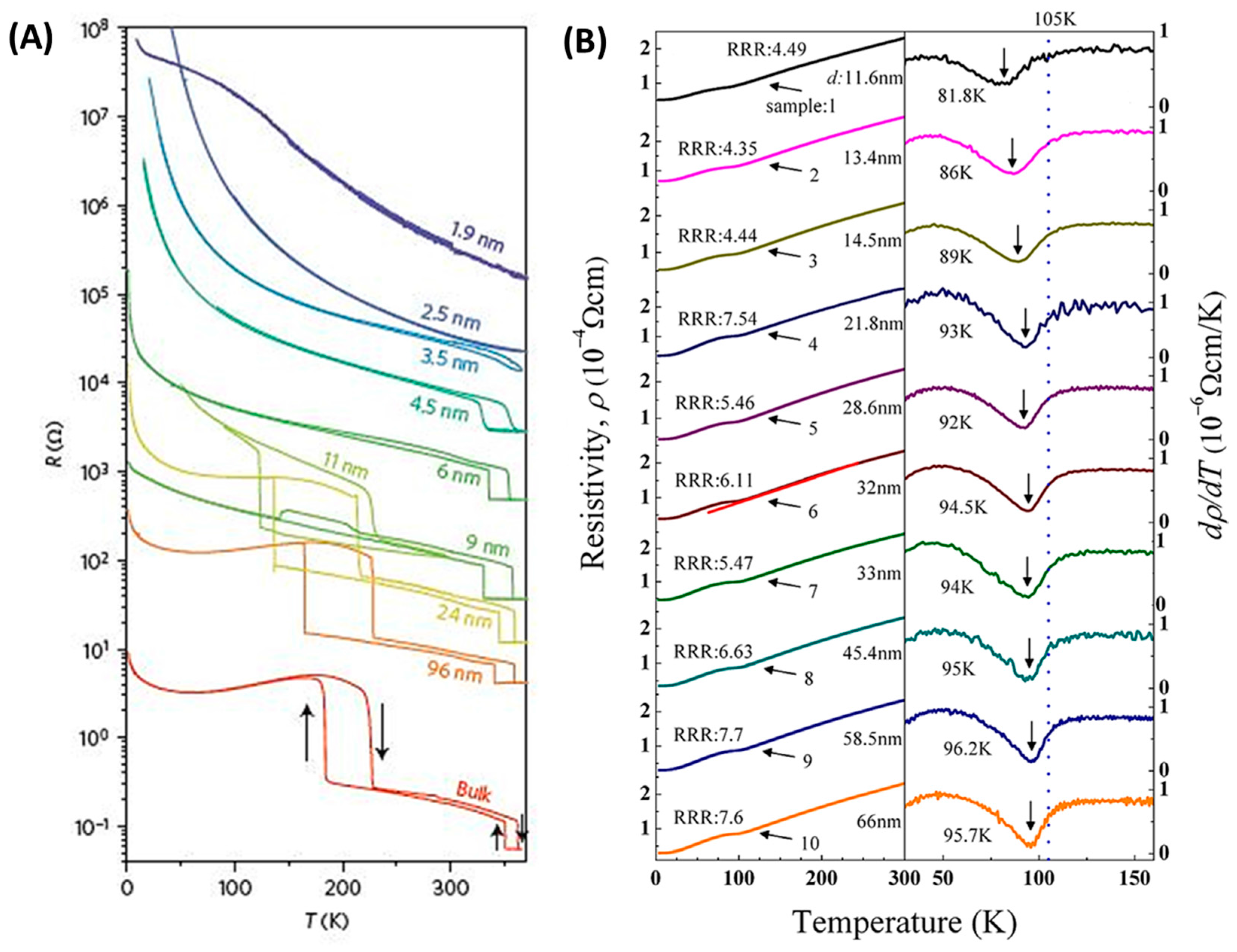
Figure 9.
(A–C) Atomically-resolved STM images of monolayer NbSe2 for various temperatures: T = 45 K (A), T = 25 K (B) and T = 5 K (C). The FFT of the STM image of (C) is shown in the inset. (D) CDW gap of monolayer NbSe2. Data are reproduced with permission from [68]. Copyright © 2015, Nature Publishing Group.

Figure 10.
(A) Planar ion migration pathways for in-plane supercapacitor using VS2 thin film electrodes. (B) Schematic illustration of the in-plane configuration of the as-fabricated supercapacitor. (C) Current-voltage at different scanning rates of 20, 100 and 200 mV/s. (D) Galvanostatic cycling behavior. (E) Galvanostatic charge/discharge curves. (F) Cycle life investigation of the supercapacitor. Data are reproduced with permission from [44]. Copyright (2011) American Chemical Society.

Figure 11.
Oscillator circuit of a 1T-TaS2 film. (A) The circuit diagram of the oscillator. (B) Voltage oscillations under different VDC values; the circuit oscillates when VDC is within the range of 3.83 V–3.95 V. (C) Load lines of the resistor at different VDC values. Data are reproduced with permission from [37]. Copyright © 2016, Nature Publishing Group.
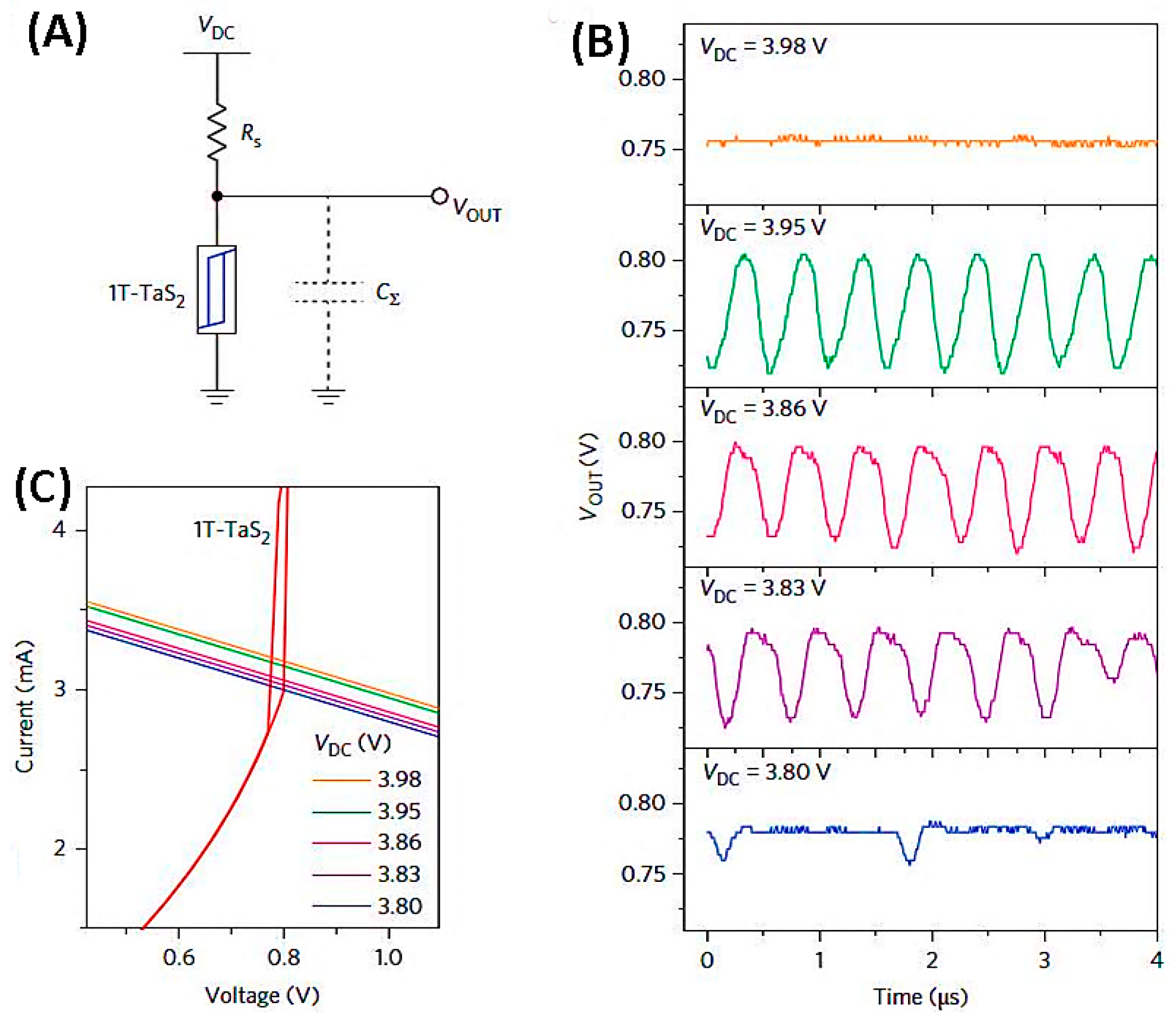
Figure 12.
(A) Photocurrent responses to the excitation wavelengths (λ) of 532 and 808 nm measured in air for the 2H-NbSe2 nanoflake with a thickness of 20 nm. A measurement under 532-nm excitation for the bulk crystal (t = 50 μm) is also shown for comparison. (B) Photocurrent, (C) responsivity and (D) photoconductive gain as a function of light intensity at 532- and 808-nm excitations for the NbSe2 nanoflake (t = 20 nm). Data are reproduced with permission from [52]. Copyright © 2015, Royal Society of Chemistry.
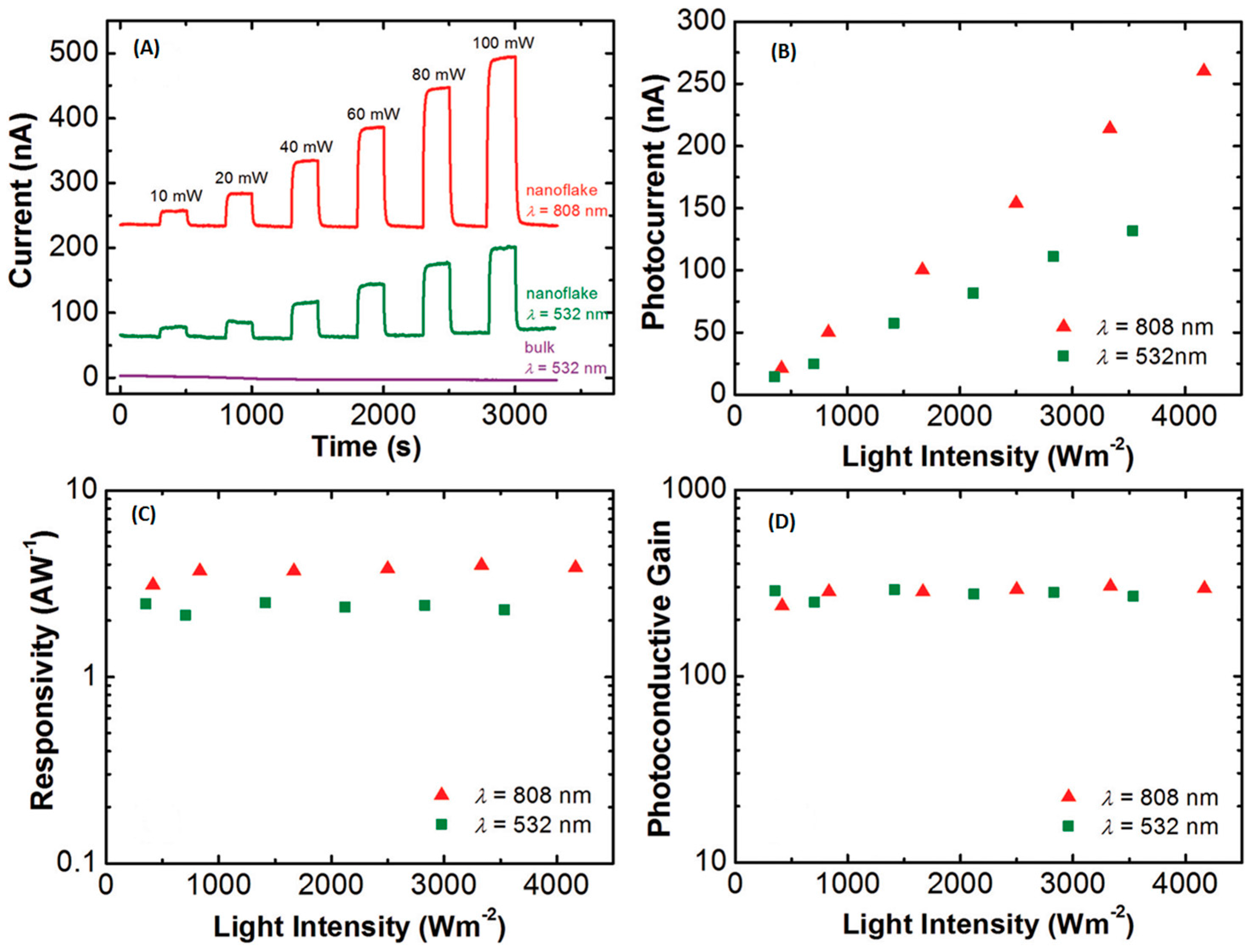
Figure 13.
Switching speed and threshold behavior of 1T-TaS2 based memory device. (A) Switching resistance ratio calculated with a single pulse upper threshold IT. (B) Erasing with 1-s pulses. (C) Schematic of the measurement circuit. (D) Voltage (V) measured during each pulse, first increasing incrementally and then reducing the pulse current (I), shown by Paths (1) and (2), respectively. (E) Same as (D), but starting from the low resistance state increasing Ipulse along Path (1) and then reducing Ipulse along (2). In all cases, T = 20 K and the pulse length was 10 µs. Scale bar, 2 µm. Data are reproduced from [38]. Copyright © 2016, Nature Publishing Group.

Figure 14.
Temperature dependent in-plane resistivity ratio of 1T-TaSe2−XTeX (A) under T = 250 K and (B) above T = 250 K. Insets: the enhancement of superconducting transitions at lower temperatures and the C-CDW transition of 1T-TaSe2 at higher temperatures. (C) Temperature dependent in-plane resistivity of 1T-TaS2–XSeX. The inset indicates the region of the superconducting transformation. (D) The NC-CDW transitions at higher temperatures of 1T-TaS2–XSeX. (E) Temperature dependence of in-plane resistivity of 4Hb-TaS2−XSeX (0 ≤ X ≤ 1.5) and the enlargement of superconducting transition at low temperature region. Data are reproduced with permission from: 1T-TaSe2−XTeX, ref. [108], Copyright (2016) American Physical Society; 1T-TaS2−XSeX, ref. [33], Copyright (2013) AIP Publishing LLC; 4Hb-TaS2−X-SeX, ref. [107], Copyright (2014) AIP Publishing LLC.

Table 1.
Phase transition of bulk CDW materials. C-CDW, commensurate CDW; NC-CDW, nearly-commensurate CDW; IC-CDW, incommensurate CDW.
Table 1.
Phase transition of bulk CDW materials. C-CDW, commensurate CDW; NC-CDW, nearly-commensurate CDW; IC-CDW, incommensurate CDW.
| Bulk Materials | Phase | Superconductivity Transition Temperature (TC) | CDW Transition Temperature (TCDW) and Structure | Crystal Phase Transition Temperature |
|---|---|---|---|---|
| VS2 | 1T | -- | ~305 K [21] | -- |
| VSe2 | 1T | -- | ~107 K [4] | -- |
| NbS2 | 2H | 6 K [22] | No CDW phase transition [22,23] | 3R→2H 1123 K |
| 3R | -- | -- | ||
| NbSe2 | 2H | 7.2 K [24] | 35 K (3 × 3 structure) [24] | 3R→2H 1104 K |
| 3R | -- | -- | ||
| TaS2 | 1T | -- | C-CDW at 180 K NC-CDW at 350 K I-CDW at 550 K [25,26] | 2H→1T 1300 K |
| 2H | 0.8 K [27] | 75 K [25] | ||
| TaSe2 | 1T | -- | C-CDW at 473 K (√13×√13 structure) I-CDW at 600 K [28] | 2H→1T 1111 K |
| 2H | 0.15 K [29] | C-CDW at 90 K (3 × 3) structure) I-CDW at 123 K [30,31] | ||
| TiSe2 | 1T | -- | ~200 K (2 × 2 structure) [11] | -- |
© 2017 by the authors. Licensee MDPI, Basel, Switzerland. This article is an open access article distributed under the terms and conditions of the Creative Commons Attribution (CC BY) license (http://creativecommons.org/licenses/by/4.0/).
Share and Cite
MDPI and ACS Style
Hossain, M.; Zhao, Z.; Wen, W.; Wang, X.; Wu, J.; Xie, L. Recent Advances in Two-Dimensional Materials with Charge Density Waves: Synthesis, Characterization and Applications. Crystals 2017, 7, 298. https://doi.org/10.3390/cryst7100298
AMA Style
Hossain M, Zhao Z, Wen W, Wang X, Wu J, Xie L. Recent Advances in Two-Dimensional Materials with Charge Density Waves: Synthesis, Characterization and Applications. Crystals. 2017; 7(10):298. https://doi.org/10.3390/cryst7100298
Chicago/Turabian StyleHossain, Mongur, Zhaoyang Zhao, Wen Wen, Xinsheng Wang, Juanxia Wu, and Liming Xie. 2017. "Recent Advances in Two-Dimensional Materials with Charge Density Waves: Synthesis, Characterization and Applications" Crystals 7, no. 10: 298. https://doi.org/10.3390/cryst7100298
Note that from the first issue of 2016, this journal uses article numbers instead of page numbers. See further details here.