Effects of Thermal Annealing on the Properties of Mechanically Exfoliated Suspended and On-Substrate Few-Layer Graphene


1
College of Engineering, Swansea University, Bay Campus, Swansea SA1 8EN, UK
2
College of Science, Taibah University, Medina 42353, Saudi Arabia
3
Centre for Nanohealth, Swansea University, Singleton Campus, Swansea SA2 8PQ, UK
*
Authors to whom correspondence should be addressed.
Crystals 2017, 7(11), 349; https://doi.org/10.3390/cryst7110349
Submission received: 25 October 2017
/
Revised: 11 November 2017
/
Accepted: 13 November 2017
/
Published: 15 November 2017
Abstract
:Graphene’s novel electrical, optical, and mechanical properties are affected both by substrate interaction and processing steps required to fabricate contacts and devices. Annealing is used to clean graphene devices, but this can lead to doping and defect changes and strain effects. There is often disagreement about which of these effects are occurring and which result in observed changes in Raman spectra. The effects of vacuum annealing on mechanically exfoliated pristine, suspended, and attached thin and thick few-layer graphene on SiO2/Si are investigated here using scanning electron microscopy (SEM), Raman spectroscopy, and atomic force microscopy (AFM). Before annealing, Raman shows that the differences in 2D and G band positions and the appearance of a disorder-induced D band of all regions were mainly because of compressive or tensile structural deformations emerging through mechanical exfoliation instead of charge doping. Annealing at low temperature is sufficient to eliminate most of the defects. However, compressive strain is induced in the sheet by annealing at high temperature, and for thin regions increased substrate conformation leads to the apparent disappearance of the sheets. The intensity ratio of the 2D and G bands also reduces with induced compressive strain, and thus should not be used to detect doping.
1. Introduction
Graphene has many novel electrical, optical, and mechanical properties that make it a promising material for building the next generation of nanoelectronics [1,2,3]. However, its properties are influenced by interactions with the environment due to the large surface-to-volume ratio [4]. Several aspects of the surrounding medium impact the behavior of graphene, including the underlying substrate and any fabrication residues. Different methods have been used to reduce or eliminate these changes, including suspending graphene sheets over holes to remove the substrate-induced changes and annealing graphene at several hundred degrees Celsius for a few hours in air or in ultra-high vacuum [5,6,7,8] to remove fabrication contamination. The effects of fabrication processes such as annealing on graphene are not fully understood, with annealing causing changes in defect density, strain, and doping [9]. There is disagreement in the literature about which of these effects are occurring and which result in the observed changes in the Raman spectra.
Raman spectroscopy has been used as a relatively quick and non-destructive technique for the characterization of graphene, as it does not require any previous sample processing steps such as depositing electrodes [10]. Raman spectroscopy is sensitive to the number of graphene layers [10,11], strain [12], and doping [9,13]. Three common features are shown in the Raman spectra of the graphene, which are the G, D, and 2D bands, appearing around 1580, 1350, and 2700 cm−1, respectively. The G band arises from the first-order scattering process related to the doubly degenerate Brillouin zone center phonon mode. The D band is caused by the breathing modes of sp2 atoms and is activated by doubly resonant disorder. It does not appear in defect-free graphene, and thus is an important indicator of the quality of the sample. The 2D peak is the most noticeable feature in the spectra. It is the second order of the D peak and is always present even when no D band appears, as no defects are needed to activate the second-order phonons [10,14]. The change of the positions and intensities of these bands is used to determine the key graphene properties, such as thickness [10,11,15], doping [13], and structural deformation [12].
In this study, we investigate the effects of annealing mechanically exfoliated pristine graphene of different thicknesses, both suspended over holes in SiO2 and attached to the substrate, by studying the changes with Raman spectroscopy, scanning electron microscopy (SEM), and atomic force microscopy (AFM). Annealing at 200 °C cleans the graphene. At higher temperatures strain effects are induced, causing wrinkles in the sheets, increased deformation, and the apparent disappearance of thin regions of graphene. The onset of these effects occurs at different temperatures for thick, thin, and suspended graphene.
2. Results and Discussion
Figure 1a shows an SEM image of a prepared graphene sample on the patterned SiO2/Si substrate. Dotted lines make clearer the boundary between areas of ‘thin’ graphene (n ~ 4) and ‘thick’ graphene (n ~ 6), with positions 1 to 4 marking the locations of the Raman spectra in Figure 1b. Spectra were normalized to the G-intensity I(G) with Table 1 showing the change of the G and 2D band positions.
Prior to annealing, differences in the Raman spectra of the graphene are evident between the areas of different thicknesses and are dependent on whether the flake is attached to the SiO2 substrate or suspended over a hole. We first establish how these characteristics compare to existing work, before we study how they change after annealing. The thickness of the layers can be determined by the G band and 2D band positions. In general the G band position downshifts while the 2D band position shifts up with increasing thickness [10,16]. The full width at half maximum (FWHM) of the 2D bands fitted by a Lorentzian function are for the thin area 60.28 cm−1, which indicates four-layer graphene, and for the thick area 69.36 cm−1, which indicates six layers [11].
Comparing the Raman spectra of the thin area (positions 2 and 1), for the suspended region the G and 2D band positions downshift with respect to the region attached to the substrate by around 1.1 cm−1 and 14 cm−1, respectively. The FWHMs of the G and 2D bands are greater than that of the attached region, broadening by around 3 cm−1 and 10 cm−1, respectively. Many experimental papers have reported Raman band shifts due to charge doping or strain [17,18,19,20,21]. Here, different charge doping can be excluded as the source of the band blue-shifts in the attached regions compared to suspended regions in our results for several reasons. First, Pisana et al. [22] and Yan et al. [23] reported that besides the G band blue-shift resulting from charge doping, a bandwidth reduction of 10 cm−1 was also observed. However, here we see a much smaller narrowing of the FWHM of the G band (3 cm−1), normally considered to be too small to be attributed to doping [19]. Also, it has been observed that charge density changes would only cause a very slight shift in the 2D-peak position [13,23], while we notice here almost a 14 cm−1 shift in the 2D band, which is too large to be caused by doping. In addition, no significant alteration in the FWHM of the 2D band has been observed experimentally [13,23], whereas we measured here a 10 cm−1 broadening in the FWHM of the 2D band of the suspended sheet. Furthermore, higher resolution SEM images of the same area shown in Figure 1 indicate a contrast increase over the holes consistent with upward bending of the suspended thin sheet, just visible in the composite image shown here. This indicates induced tensile strain in this region through the transfer process, leading to the observed shifts in the G and 2D band positions. While the D-peak position is not usually included in similar studies, we include it for reference in Table 1 [12,24].
The very small downshift of the 2D band (less than 1 cm−1) can be seen in the suspended region of the thick graphene layer compared to the attached part, while no change in the G band peak position is observed because the thick graphene sheet has higher rigidity and therefore resists bending from non-planarity [16]. These results show that the differences in the 2D and G band positions of the few-layer graphene are because of compressive or tensile structural deformations emerging through mechanical exfoliation instead of charge doping, which reduce with increasing thickness [4].
Another feature evident in all spectra of Figure 1b and Figure 2, prior to annealing, is the D band, positioned at around 1350 cm−1, indicating the presence of defects in the graphene sample. It is clear that the D band intensity I(D) in the thin sheet is higher than that of the thick graphene sheet in both the suspended and attached regions. Also, the I(D) of the suspended thin layer is higher than the one attached to the substrate—however, these values are smaller than that reported for good quality thin layers of graphene [19]. This is confirmed in Figure 3a, which illustrates the ratio of the intensities between D and G bands I(D)/I(G). This ratio is commonly used to estimate the number of defects in carbon materials. In addition to the D band peak, two additional weak bands at around 1460 cm−1 and 1620 cm−1, and a feature at around 2930 cm−1, were observed in the spectra in both the suspended and attached thin graphene areas, which also are induced by defects [25]. These additional Raman bands were absent in suspended and attached regions of the thick graphene layer. Additionally, the I(D)/I(G) of both locations of thick graphene sheet is extremely low (~2%), which demonstrates that defects are much easier to introduce in the thinner sheets of graphene.
The origin of the thickness dependence of the D band scattering in graphene sheets is suggested to be caused by the rigidity of the graphene sheets, which reduces with reduction number of graphene layers [16]. Relatively speaking, the thinner layers are extremely compliant and deform easily when deposited onto the SiO2/Si substrates through the van der Waals coupling between the substrates and graphene layers. However, the thicker layers are considerably more rigid and show more resistance against bending from non-planarity. Sometimes the I(D) is lower in suspended graphene because of the reduction in substrate interaction. However, in our samples the suspended region of the thin area is bending and the intensities of the strong and weak disorder-induced bands are higher than the attached region, which demonstrates that the deformation leads to increased intensities of the disorder-induced bands. Again, this confirms that the differences in the 2D and G band positions of the suspended and attached thin graphene are because of structural deformations emerging through mechanical exfoliation instead of charge doping.
Next, we address the changes in the Raman spectra of these layers as the samples are annealed. Figure 2 shows the Raman spectra before and after annealing in ultra-high vacuum (UHV). The most apparent feature can be seen after annealing graphene at 200 °C: the disappearance of the D band or reduction of its intensity. Also, the weak bands at around 1620 cm−1, 1460 cm−1, and 2930 cm−1 of the suspended thin graphene sheet are removed. The feature at 1460 cm−1 is close to an R-band feature observed by others around 1505 cm−1 which has been attributed to folding or bending in the graphene, which could be the result of the transfer process affecting the thin sample area more [26]. As it is removed here after annealing, it would suggest that the mechanical change in the graphene sheets has removed this feature. No significant difference is seen in annealing the graphene layers at 300 °C; however, annealing at higher temperatures leads to increases in the intensity of the D band of the attached sheets and suspended thick sheet.
The changes in the intensity of the D band as the annealing temperature increases are further demonstrated in Figure 3a by plotting the change in the I(D)/I(G) ratio. Moreover, the broadness of the G band can be clearly observed in all spectra (Figure 2) as the annealing temperature increases to 400 °C and 500 °C. These observations demonstrate an increase in the quality of the graphene layers by annealing graphene at low temperatures, whereas annealing at high temperatures (>300 °C) can lead to the induction of some structural disorder in the graphene samples, demonstrated by the appearance or the increase of the D band intensity and the increase in the width of the G band.
The induced defects in the graphene samples could be caused by the effects of doping or strain. Various different parameters have been used in the literature to differentiate between the effects of doping and strain, including the intensity ratios between the 2D and G bands (I(2D)/I(G)) and between the D and 2D bands (I(D)/I(2D)), and a comparison of the shifts of the G and 2D bands and the FWHM of the G band [9,18,19,27,28,29]. Whilst most papers study one or two of these parameters, here we compare all of them to bring together the various results. Figure 3b shows the effect of thermal annealing on the I(2D)/I(G) ratio of the graphene. An apparent observation is that, for the suspended thin layer and both locations of the thick layer, this ratio decreases above annealing at 300 °C. However, for the thin layer attached to the substrates, it decreases linearly through annealing. The reduction in the I(2D)/I(G) ratio in annealed graphene samples has been attributed to doping effects. However, in our results, we found that these changes with annealing were caused by strain effects, as will be demonstrated later in the text.
There are several reasons why we can exclude doping as the cause of the I(2D)/I(G) changes in our experiment. Firstly, besides the decrease of the I(2D)/I(G) ratio, a G band upshift with a FWHM narrowing was also detected in the case of doping [9,18,28]. However, in our experiments, a clear broadening of the FWHM of the G band is observed after thermal annealing at 400 °C and 500 °C, as shown in Figure 2 and Figure 3d. Secondly, it has also been reported that, besides the reduction of the I(2D)/I(G) ratio, the ratio of I(D)/I(2D) does not change with doping while the ratio of I(D)/I(G) reduces [29]. Yet, in our results, I(D)/I(G) increases over 300 °C and I(D)/I(2D) changes with thermal annealing and shows the same behavior of I(D)/I(G), as illustrated in Figure 3a,c. These observations indicate that the effect of the doping on our results can be excluded.
On the other hand, many papers have demonstrated a blue shift of the band positions in thermally annealed graphene samples due to compressive strain in the graphene layers [19,27,30], which corresponds with what we observed in our results; the stiffening (shift to higher frequency) of G, D, and 2D bands after annealing at 500 °C was seen for all regions both suspended and attached to the substrate. Table 2 shows the frequency upshifts of the Raman G (ΔωG), D (ΔωD), and 2D (Δω2D) bands of the graphene sheet with different locations after annealing at 500 °C.
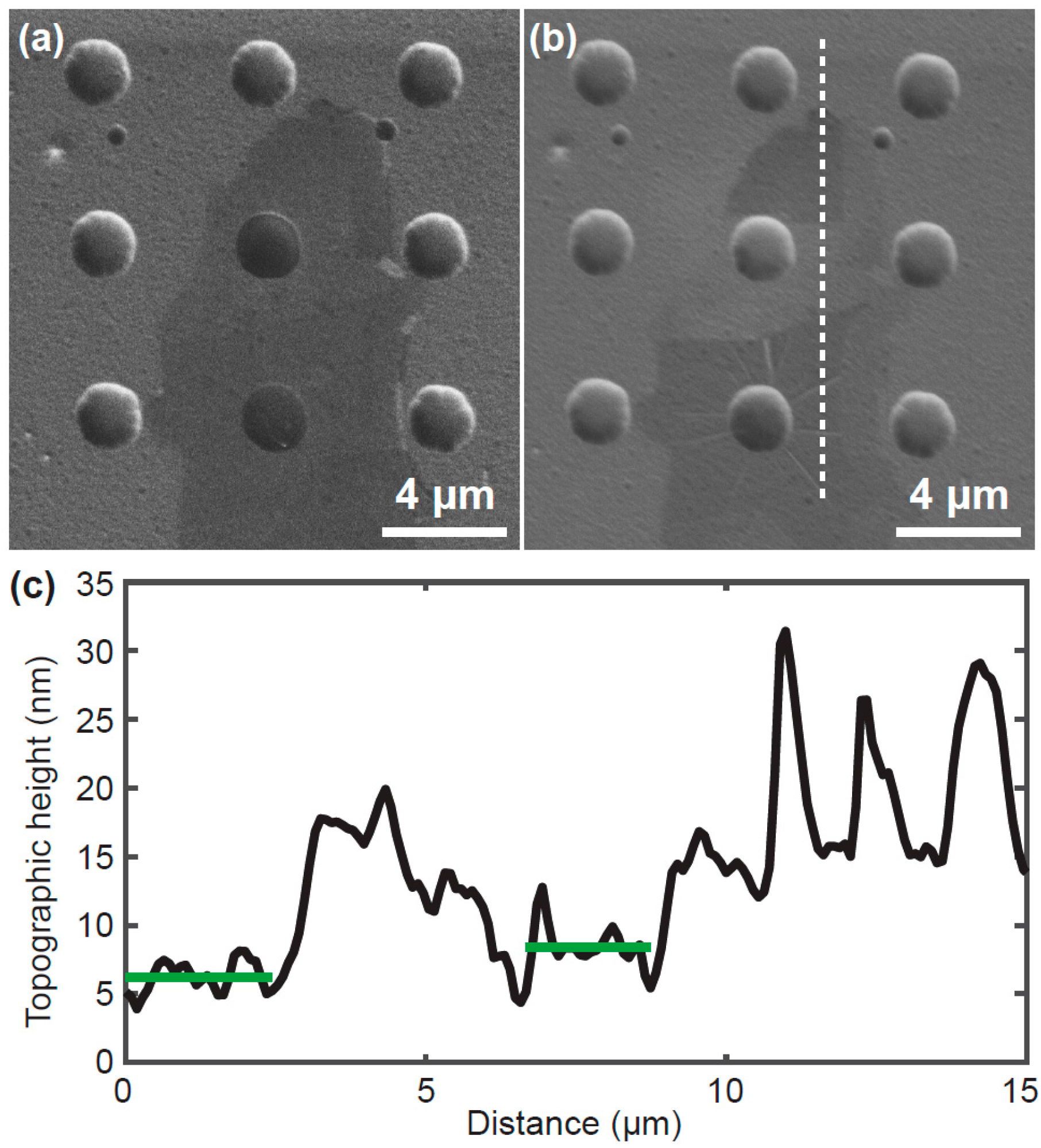
The effects of compressive strain can be seen clearly in the SEM image in Figure 4b where several ‘wrinkles’ were created, leading in to the hole in the thick region after annealing at 500 °C. They were not present when only annealed to 200 °C, as shown in Figure 4a.
Perhaps the most notable feature of Figure 4b is the apparent disappearance in SEM of the thin region after annealing at 500 °C, while the thicker regions of the flake above and below are still present. This effect has been attributed in the literature to a reduction in the number of graphene layers blown off or absorbed into the substrate during annealing [19]. However, here the Raman spectra in Figure 2 indicate that the thin region is still present, with increased strain effects. An AFM line scan down the dotted white line shown in Figure 4b is shown again in Figure 4c, where the horizontal lines are the mean height for the SiO2 region and the thin graphene layer, respectively. Although the AFM scan is noisy due to the induced structural ripples from annealing, the average lines show that the thin region is still 2.20 nm higher than the SiO2 substrate, confirming the Raman observation that the thin graphene layer is still there, but no longer visible under SEM. We believe that the induced compressive strain caused the graphene to conform to the underlying SiO2 substrate roughness, such that it is indistinguishable from the substrate by SEM. The thicker areas are less elastic than the thinner regions and therefore do not undergo the same conformation when annealed. Calculations of the expected thickness of four-layer graphene measured with AFM are in the region of 2.3 to 2.5 nm [31,32,33]. These estimates are made up of an initial graphene-substrate offset of at least 1 nm plus the height of each graphene layer. With the increased substrate conformation following annealing, the graphene-substrate offset was reduced and the total height of 2.20 nm corresponds to four-layer graphene, matching the Raman estimate of the layer number.
To bring all these results together, we attribute the reduction in the 2D/G height ratio of both the suspended thin and thick layers and the attached thick layer at annealing temperatures higher than 300 °C, as well as the attached thin layer at a temperature of 200 °C, to the created deformations in the sheet as a result of the compressive strain during annealing. Graphite and graphene have a negative thermal expansion coefficient [34,35,36,37], whereas the SiO2 substrate has a positive thermal expansion coefficient. Typically, the graphene layers hold to the substrate by van der Waals forces. In the case of suspended and/or thick sheet, the van der Waals interaction becomes smaller. Thus, the variance in the thermal expansion coefficients is negligible when annealing the sheet at low temperature, as the induced tensile strain is small and the graphene sheets return to their original state after cooling [30]. However, the mismatch in thermal expansion coefficients leads to induced compressive strain when the graphene sheets are annealed at high temperatures [38]. The graphene sheet will slip across the SiO2 surface as a result of significant increases in the induced tensile strain above the van der Waals forces holding the graphene onto the SiO2 substrate as the temperature rises.
Slippages occurred in our suspended layers and attached thick layer at annealing temperatures higher than 300 °C. On the other hand, in the attached thin layer, the 2D/G height ratio linearly reduced with the annealing temperature. This is because the van der Waals interaction between the graphene and the SiO2/Si substrate is higher in thinner sheets [1]. Thus, annealing the sample at low temperature leads to large induced strain and the slippage occurs at temperatures of around 200 °C, which is the same value reported for single- and bi-layer grapheme [30]. The degree of the slippage depends on the annealing temperature, and it increases as the temperature rises. When the temperature drops back to room temperature, compressive strain emerges in the graphene sheet, which leads to the sheets buckling and forming ripples.
Enhanced charge scattering was reported as a reason for the reduction in the I(2D)/I(G) ratio in doped graphene because of doping changes [39]. However, ripples and deformations in the graphene sheets also lead to increased charge scattering, which is the reason for reduced mobility and conductivity [40,41,42]. This confirms that the I(2D)/I(G) ratio also reduces because of induced compressive strain. Moreover, the result reported here indicates that the I(2D)/(G) ratio changes should not be used as a parameter to monitor the doping level, since it also changes because of the existence of ripples and deformations in the graphene sheets.
3. Experimental
Graphene samples were prepared by the mechanical exfoliation of highly oriented pyrolytic graphite (HOPG) using Scotch tape and deposited onto pre-etched SiO2/Si substrates to create suspended sheets over the holes [1,43]. The patterned samples were prepared by first defining arrays of circles with a diameter of 1.6 μm by electron beam lithography on a Si wafer, which were then plasma etched to a depth of 800 nm [44]. Following this, a 90-nm-thick SiO2 layer was grown by thermal oxidation. SEM was used to locate the suspended graphene sheets and then Raman spectroscopy was used to determine the thickness and the quality of the sheets. Samples were then annealed in an ultra-high vacuum (UHV) to prevent the oxidation of the graphene by interacting with ambient air [20] at 200, 300, 400, and 500 °C for an hour. Raman spectra were measured using a Renishaw inVia Raman microscope, at room temperature using a laser with an incident power of 2.64 mW to avoid sample damage or laser-induced heating [10], and a wavelength of 532 nm was focused on both regions that were suspended and attached to the SiO2/Si substrate of both thicknesses of few-layer graphene (hereafter called thin and thick) using a 50× objective. The spectra were taken with a 10-second exposure time, with three accumulations to enhance the signal-to-noise ratio. Raman spectra were obtained on annealed graphene sheets to study the effects of thermal annealing. Each Raman spectrum was measured at the same position after each annealing temperature and then normalized by the G intensity. Lastly, AFM was used under ambient conditions in contact mode using a Nanosurf NaioAFM to show height profiles of the attached graphene layers to the substrate after annealing the sample at 500 °C.
4. Conclusions
Annealing is usually a required stage in fabricating graphene devices, which also provides a straightforward way to improve the quality of the sheets. However, there is disagreement in the literature about the effects of annealing on the subject of strain and charge doping. Some research concluded that annealing alters the doping, by dopant transfer from the environment or the substrate, or out-gassing of dopants in doped graphene samples [28,45]. Other papers reported that compressive strain is induced in samples after annealing and that this is a competing explanation for the observed changes [19,27]. This has been investigated in the present work using Raman spectroscopy on mechanically exfoliated pristine, suspended, and attached thin and thick few-layer graphene, deposited under ambient conditions without any extra processing.
Before annealing, the results confirm that the differences in the 2D and G band positions, and the appearance of the disorder-induced D band in few-layer graphene, were mainly because of compressive or tensile structural deformations emerging through mechanical exfoliation. These do not occur as a result of doping changes, which have been identified as the cause of such spectral changes [14]. These disorder-induced changes were observed much more clearly in the thin layer, because the thick layer has higher rigidity and therefore resists conforming to the substrate during deposition.
Annealing at low temperatures led to a reduction or elimination of defects, while annealing at elevated temperatures induced structural disorder in the graphene sheet, demonstrated by the reduction of the I(2D)/I(G) ratio. We attribute the change in the I(2D)/I(G) with annealing to the ripple formation created because of compressive stress on the graphene since it is associated with the stiffening of the G and 2D band, as well as the broadening of the G band.
Thin regions of a continuous flake of graphene were observed to apparently disappear in SEM after annealing at 500 °C, which has been attributed elsewhere to a reduction or removal of the graphene layers. However, here we show with Raman and AFM that the sheets were still present, but had conformed to the underlying substrate topography such that there is no evident contrast difference in SEM. The thicker regions of the same flake do not undergo the strain-induced conformation and remain visible.
We conclude that the I(2D)/I(G) ratio should not be used as a parameter to monitor the doping level as reported in the literature, because this parameter also reduces because of the existence of ripples and deformations in the sheet. The results indicate that the deformation can be increased on the graphene sheets with thermal annealing, which leads to changes in the electronic and structure properties of the graphene, and this effect must be considered in all graphene studies.
Acknowledgments
Mona M. M. Alyobi thanks a Saudi Scholarship (Taibah University, Kingdom of Saudi Arabia) for financial support.
Author Contributions
Mona M. M. Alyobi and Richard J. Cobley performed the experiments, with support from Chris J. Barnett. Mona M. M. Alyobi analyzed the data and wrote the paper. Richard J. Cobley co-wrote the paper and supervised the research. All authors read and approved the final manuscript.
Conflicts of Interest
The authors declare no conflict of interest.
References
- Novoselov, K.S.; Geim, A.K.; Morozov, S.; Jiang, D.; Zhang, Y.; Dubonos, S.; Grigorieva, I.V.; Firsov, A.A. Electric field effect in atomically thin carbon films. Science 2004, 306, 666–669. [Google Scholar] [CrossRef] [PubMed]
- Geim, A.K.; Novoselov, K.S. The rise of graphene. Nat. Mater. 2007, 6, 183–191. [Google Scholar] [CrossRef] [PubMed]
- Cooper, D.R.; D’Anjou, B.; Ghattamaneni, N.; Harack, B.; Hilke, M.; Horth, A.; Majlis, N.; Massicotte, M.; Vandsburger, L.; Whiteway, E.; et al. Experimental review of graphene. ISRN Condens. Matter Phys. 2012, 2012. [Google Scholar] [CrossRef]
- Kim, S.; Ryu, S. Thickness-dependent native strain in graphene membranes visualized by Raman spectroscopy. Carbon 2016, 100, 283–290. [Google Scholar] [CrossRef]
- Geringer, V.; Liebmann, M.; Echtermeyer, T.; Runte, S.; Schmidt, M.; Rückamp, R.; Lemme, M.; Morgenstern, M. Intrinsic and extrinsic corrugation of monolayer graphene deposited on SiO2. Phys. Rev. Lett. 2009, 102, 76102. [Google Scholar] [CrossRef] [PubMed]
- Mashoff, T.; Pratzer, M.; Geringer, V.; Echtermeyer, T.; Lemme, M.C.; Liebmann, M.; Morgenstern, M. Bistability and oscillatory motion of natural nanomembranes appearing within monolayer graphene on silicon dioxide. Nano Lett. 2010, 10, 461–465. [Google Scholar] [CrossRef] [PubMed]
- Bolotin, K.I.; Sikes, K.; Jiang, Z.; Klima, M.; Fudenberg, G.; Hone, J.; Kim, P.; Stormer, H.L. Ultrahigh electron mobility in suspended graphene. Solid State Commun. 2008, 146, 351–355. [Google Scholar] [CrossRef]
- Lin, Y.-C.; Lu, C.-C.; Yeh, C.-H.; Jin, C.; Suenaga, K.; Chiu, P.-W. Graphene Annealing: How Clean Can It Be? Nano Lett. 2012, 12, 414–419. [Google Scholar] [CrossRef] [PubMed]
- Chen, C.-C.; Bao, W.; Chang, C.-C.; Zhao, Z.; Lau, C.N.; Cronin, S.B. Raman spectroscopy of substrate-induced compression and substrate doping in thermally cycled graphene. Phys. Rev. B 2012, 85, 35431. [Google Scholar] [CrossRef]
- Ferrari, A.; Meyer, J.; Scardaci, V.; Casiraghi, C.; Lazzeri, M.; Mauri, F.; Piscanec, S.; Jiang, D.; Novoselov, K.S.; Roth, S.; et al. Raman spectrum of graphene and graphene layers. Phys. Rev. Lett. 2006, 97, 187401. [Google Scholar] [CrossRef] [PubMed]
- Hao, Y.; Wang, Y.; Wang, L.; Ni, Z.; Wang, Z.; Wang, R.; Koo, C.K.; Shen, Z.; Thong, J.T. Probing Layer Number and Stacking Order of Few-Layer Graphene by Raman Spectroscopy. Small 2010, 6, 195–200. [Google Scholar] [CrossRef] [PubMed]
- Mohiuddin, T.M.G.; Lombardo, A.; Nair, R.R.; Bonetti, A.; Savini, G.; Jalil, R.; Bonini, N.; Basko, D.M.; Galiotis, C.; Marzari, N.; et al. Uniaxial strain in graphene by Raman spectroscopy: G peak splitting, Grüneisen parameters, and sample orientation. Phys. Rev. B 2009, 79, 205433. [Google Scholar] [CrossRef]
- Stampfer, C.; Molitor, F.; Graf, D.; Ensslin, K.; Jungen, A.; Hierold, C.; Ensslin, K. Raman imaging of doping domains in graphene on SiO2. Appl. Phys. Lett. 2007, 91, 241907. [Google Scholar] [CrossRef]
- Casiraghi, C.; Pisana, S.; Novoselov, K.; Geim, A.; Ferrari, A. Raman fingerprint of charged impurities in graphene. Appl. Phys. Lett. 2007, 91, 233108. [Google Scholar] [CrossRef]
- Graf, D.; Molitor, F.; Ensslin, K.; Stampfer, C.; Jungen, A.; Hierold, C.; Wirtz, L. Spatially resolved Raman spectroscopy of single-and few-layer graphene. Nano Lett. 2007, 7, 238–242. [Google Scholar] [CrossRef] [PubMed]
- Gupta, A.; Chen, G.; Joshi, P.; Tadigadapa, S.; Eklund, P. Raman scattering from high-frequency phonons in supported n-graphene layer films. Nano Lett. 2006, 6, 2667–2673. [Google Scholar] [CrossRef] [PubMed]
- Berciaud, S.; Ryu, S.; Brus, L.E.; Heinz, T.F. Probing the intrinsic properties of exfoliated graphene: Raman spectroscopy of free-standing monolayers. Nano Lett. 2008, 9, 346–352. [Google Scholar] [CrossRef] [PubMed]
- Das, A.; Pisana, S.; Chakraborty, B.; Piscanec, S.; Saha, S.K.; Waghmare, U.V.; Novoselov, K.S.; Krishnamurthy, H.R.; Geim, A.K.; Ferrari, A.C.; et al. Monitoring dopants by Raman scattering in an electrochemically top-gated graphene transistor. Nat. Nano 2008, 3, 210–215. [Google Scholar] [CrossRef] [PubMed]
- Ni, Z.H.; Wang, H.M.; Ma, Y.; Kasim, J.; Wu, Y.H.; Shen, Z.X. Tunable stress and controlled thickness modification in graphene by annealing. ACS Nano 2008, 2, 1033–1039. [Google Scholar] [CrossRef] [PubMed]
- Metzger, C.; Rémi, S.; Liu, M.; Kusminskiy, S.V.; Neto, A.H.C.; Swan, A.K.; Goldberg, B.B. Biaxial strain in graphene adhered to shallow depressions. Nano Lett. 2009, 10, 6–10. [Google Scholar] [CrossRef] [PubMed]
- Huang, C.H.; Lin, H.Y.; Huang, C.W.; Liu, Y.M.; Shih, F.Y.; Wang, W.H.; Chui, H. Probing substrate influence on graphene by analyzing Raman lineshapes. Nanoscale Res. Lett. 2014, 9. [Google Scholar] [CrossRef] [PubMed]
- Pisana, S.; Lazzeri, M.; Casiraghi, C.; Novoselov, K.S.; Geim, A.K.; Ferrari, A.C.; Mauri, F. Breakdown of the adiabatic Born–Oppenheimer approximation in graphene. Nat. Mater. 2007, 6, 198–201. [Google Scholar] [CrossRef] [PubMed]
- Yan, J.; Zhang, Y.; Kim, P.; Pinczuk, A. Electric field effect tuning of electron-phonon coupling in graphene. Phys. Rev. Lett. 2007, 98, 166802. [Google Scholar] [CrossRef] [PubMed]
- Huang, M.; Yan, H.; Chen, C.; Song, D.; Heinz, T.F.; Hone, J. Phonon softening and crystallographic orientation of strained graphene studied by Raman spectroscopy. Proc. Natl. Acad. Sci. USA 2009, 106, 7304–7308. [Google Scholar] [CrossRef] [PubMed]
- Pimenta, M.A.; Dresselhaus, G.; Dresselhaus, M.S.; Cancado, L.G.; Jorio, A.; Saito, R. Studying disorder in graphite-based systems by Raman spectroscopy. Phys. Chem. Chem. Phys. 2007, 9, 1276–1291. [Google Scholar] [CrossRef] [PubMed]
- Qiu, C.; Bennet, K.E.; Khan, T.; Ciubuc, J.D.; Manciu, F.S. Raman and Conductivity Analysis of Graphene for Biomedical Applications. Materials 2016, 9, 897. [Google Scholar] [CrossRef] [PubMed]
- Chen, C.C.; Bao, W.; Theiss, J.; Dames, C.; Lau, C.N.; Cronin, S.B. Raman spectroscopy of ripple formation in suspended graphene. Nano Lett. 2009, 9, 4172–4176. [Google Scholar] [CrossRef] [PubMed]
- Ryu, S.; Liu, L.; Berciaud, S.; Yu, Y.-J.; Liu, H.; Kim, P.; Flynn, G.W.; Brus, L.E. Atmospheric oxygen binding and hole doping in deformed graphene on a SiO2 substrate. Nano Lett. 2010, 10, 4944–4951. [Google Scholar] [CrossRef] [PubMed]
- Bruna, M.; Ott, A.K.; Ijäs, M.; Yoon, D.; Sassi, U.; Ferrari, A.C. Doping dependence of the Raman spectrum of defected graphene. ACS Nano 2014, 8, 7432–7441. [Google Scholar] [CrossRef] [PubMed]
- Yoon, D.; Son, Y.W.; Cheong, H. Negative thermal expansion coefficient of graphene measured by Raman spectroscopy. Nano Lett. 2011, 11, 3227–3231. [Google Scholar] [CrossRef] [PubMed]
- Li, X.; Wang, X.; Zhang, L.; Lee, S.; Dai, H. Chemically derived, ultrasmooth graphene nanoribbon semiconductors. Science 2008, 319, 1229–1232. [Google Scholar] [CrossRef] [PubMed]
- Li, X.-L.; Qiao, X.-F.; Han, W.-P.; Lu, Y.; Tan, Q.-H.; Liu, X.-L.; Tan, P.-H. Layer number identification of intrinsic and defective multilayered graphenes up to 100 layers by the Raman mode intensity from substrates. Nanoscale 2015, 7, 8135–8141. [Google Scholar] [CrossRef] [PubMed]
- Lin, Y.M.; Avouris, P. Strong suppression of electrical noise in bilayer graphene nanodevices. Nano Lett. 2008, 8, 2119–2125. [Google Scholar] [CrossRef] [PubMed]
- Steward, E.; Cook, B.; Kellett, E. Dependence on temperature of the interlayer spacing in carbons of different graphitic perfection. Nature 1960, 187, 1015–1016. [Google Scholar] [CrossRef]
- Zakharchenko, K.; Katsnelson, M.; Fasolino, A. Finite temperature lattice properties of graphene beyond the quasiharmonic approximation. Phys. Rev. Lett. 2009, 102, 46808. [Google Scholar] [CrossRef] [PubMed]
- Jiang, J.-W.; Wang, J.-S.; Li, B. Thermal expansion in single-walled carbon nanotubes and graphene: Nonequilibrium Green’s function approach. Phys. Rev. B. 2009, 80, 205429. [Google Scholar] [CrossRef]
- Bao, W.; Miao, F.; Chen, Z.; Zhang, H.; Jang, W.; Dames, C.; Lau, C.N. Controlled ripple texturing of suspended graphene and ultrathin graphite membranes. Nat. Nanotechnol. 2009, 4, 562–566. [Google Scholar] [CrossRef] [PubMed]
- Lee, J.E.; Ahn, G.; Shim, J.; Lee, Y.S.; Ryu, S. Optical separation of mechanical strain from charge doping in graphene. Nat. Commun. 2012, 3, 1024. [Google Scholar] [CrossRef] [PubMed]
- Basko, D.; Piscanec, S.; Ferrari, A. Electron-electron interactions and doping dependence of the two-phonon Raman intensity in graphene. Phys. Rev. B 2009, 80, 165413. [Google Scholar] [CrossRef]
- Schedin, F.; Geim, A.K.; Morozov, S.V.; Hill, E.W.; Blake, P.; Katsnelson, M.I.; Novoselov, K.S. Detection of individual gas molecules adsorbed on graphene. Nat. Mater. 2007, 6, 652–655. [Google Scholar] [CrossRef] [PubMed] [Green Version]
- Gazit, D. Theory of the spontaneous buckling of doped graphene. Phys. Rev. B 2009, 79, 113411. [Google Scholar] [CrossRef]
- Katsnelson, M.; Geim, A. Electron scattering on microscopic corrugations in graphene. Philos. Trans. R. Soc. Lond. A Math. Phys. Eng. Sci. 2008, 366, 195–204. [Google Scholar] [CrossRef] [PubMed]
- Novoselov, K.S.; Jiang, D.; Schedin, F.; Booth, T.J.; Khotkevich, V.V.; Morozov, S.V.; Geim, A.K. Two-dimensional atomic crystals. Proc. Natl. Acad. Sci. USA 2005, 102, 10451–10453. [Google Scholar] [CrossRef] [PubMed]
- Alyobi, M.; Cobley, R. Electron Beam Lithography and Plasma Etching To Fabricate Supports for Studying Nanomaterials. Int. J. Res. Sci. 2017, 3, 18–21. [Google Scholar] [CrossRef]
- Ni, Z.H.; Wang, H.M.; Luo, Z.Q.; Wang, Y.Y.; Yu, T.; Wu, Y.H.; Shen, Z.X. The effect of vacuum annealing on graphene. J. Raman Spectrosc. 2010, 41, 479–483. [Google Scholar] [CrossRef]
Figure 1.
(a) SEM image and (b) Raman spectra of ‘thin’ and ‘thick’ regions of the graphene attached to the SiO2/Si substrate (locations 1 and 3, respectively) and suspended regions (locations 2 and 4). All spectra are normalized by the G-intensity. Dashed lines on the SEM image indicate the boundary between different thicknesses for clarity.
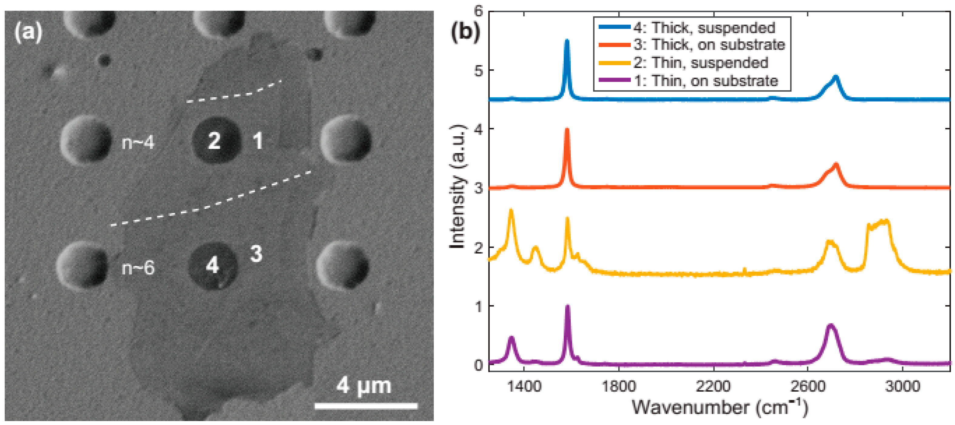
Figure 2.
Raman spectra of (a) location 1: thin, on substrate; (b) location 2: thin, suspended; (c) location 3: thick, on substrate; (d) location 4: thick, suspended. Spectra are offset vertically by increasing the temperature from bottom to top, before annealing and after annealing at 200, 300, 400, and 500 °C, respectively. Spectra are normalized by the G band intensity.
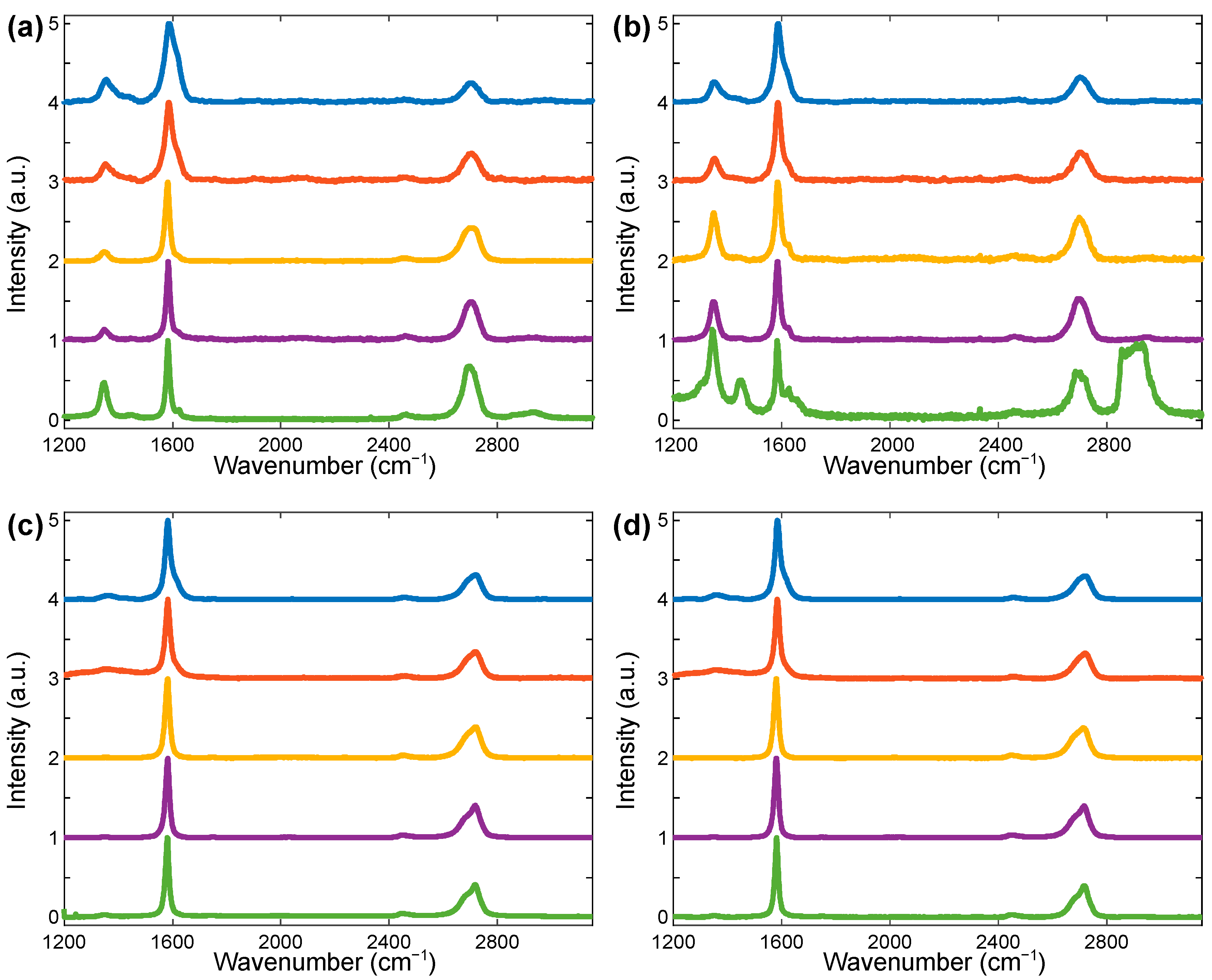
Figure 3.
The ratio intensities of I(D)/I(G) in (a), I(2D)/I(G) (b), and I(D)/I(2D) (c) of graphene sheet with different locations before and after annealing at different annealing temperatures; (d) G band full width at half maximum (FWHM) of graphene sheets with different locations before and after annealing at different annealing temperatures, the FWHM of the G band was fitted using the Lorentzian function—dashed lines aid the reader to see overlapping points.
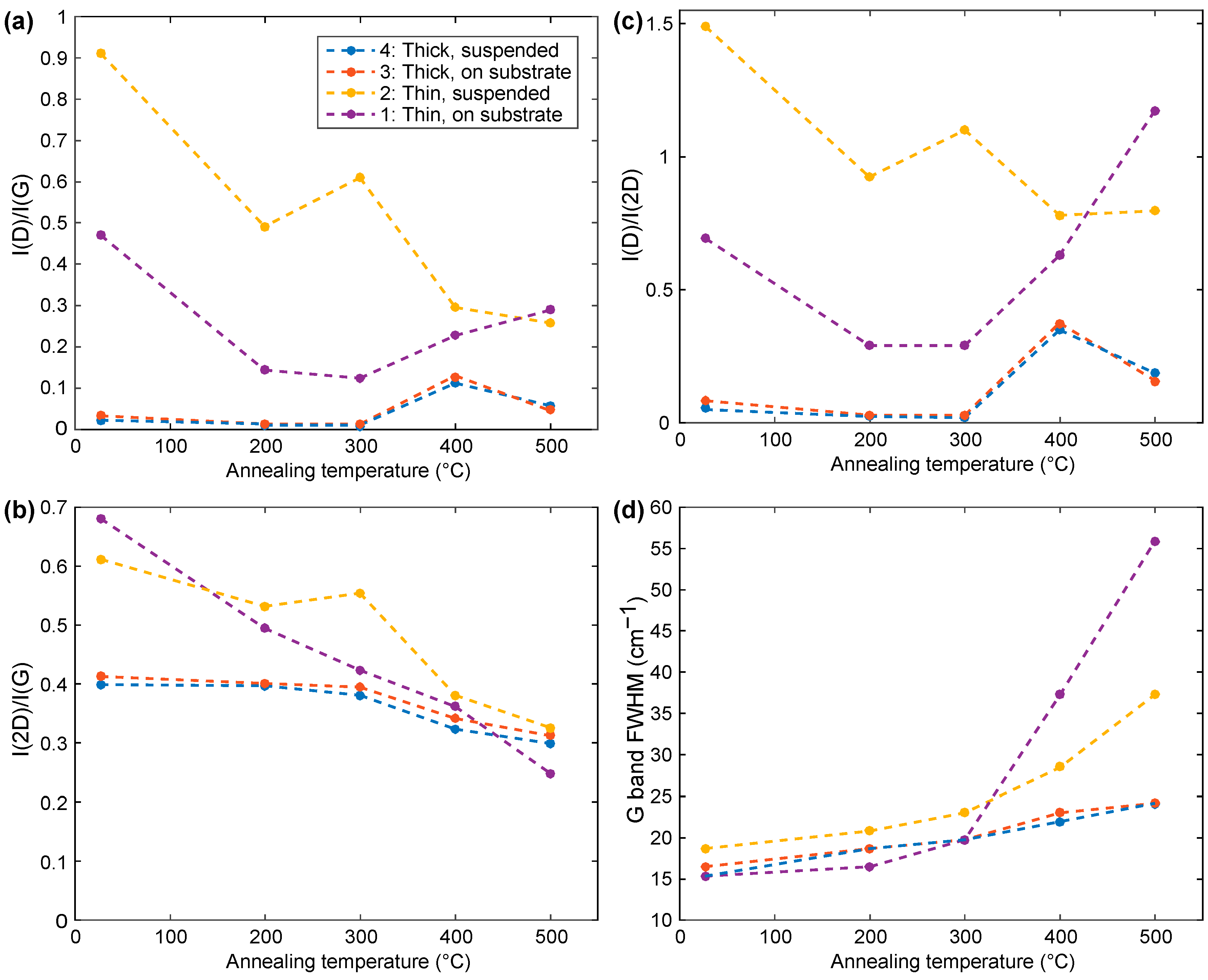
Figure 4.
(a) SEM image of the sample after annealing at 200 °C, (b) SEM image after annealing at 500 °C, and (c) an atomic force microscopy (AFM) height profile down the dotted line indicated in (b) with two mean heights marked for (left) the SiO2 substrate and (right) the attached thin region.
Figure 4.
(a) SEM image of the sample after annealing at 200 °C, (b) SEM image after annealing at 500 °C, and (c) an atomic force microscopy (AFM) height profile down the dotted line indicated in (b) with two mean heights marked for (left) the SiO2 substrate and (right) the attached thin region.

Table 1.
Values of G and 2D band positions of thin and thick graphene layers.
| Thin Layer (≈4 Layers) | Thick Layer (≈6 Layers) | |||
|---|---|---|---|---|
| On Substrate | Suspended | On Substrate | Suspended | |
| G position (cm−1) | 1583.80 | 1582.71 | 1580.51 | 1580.51 |
| 2D position (cm−1) | 2697.28 | 2683.56 | 2717.35 | 2716.44 |
| D position (cm−1) | 1345.84 | 1343.56 | 1346.98 | 1348.11 |
Table 2.
The frequency upshifts of the Raman G (ΔωG), D (ΔωD), and 2D (Δω2D) bands of graphene sheet with different locations after annealing at 500 °C.
Table 2.
The frequency upshifts of the Raman G (ΔωG), D (ΔωD), and 2D (Δω2D) bands of graphene sheet with different locations after annealing at 500 °C.
| Thin Layer | Thick Layer | |||
|---|---|---|---|---|
| On Substrate | Suspended | On Substrate | Suspended | |
| ΔωG (cm−1) | 4.38 | 3.28 | 2.18 | 3.28 |
| ΔωD (cm−1) | 9.08 | 7.95 | 9.08 | 9.08 |
| Δω2D (cm−1) | 10.03 | 16.45 | 1.81 | 3.63 |
© 2017 by the authors. Licensee MDPI, Basel, Switzerland. This article is an open access article distributed under the terms and conditions of the Creative Commons Attribution (CC BY) license (http://creativecommons.org/licenses/by/4.0/).
Share and Cite
MDPI and ACS Style
Alyobi, M.M.M.; Barnett, C.J.; Cobley, R.J. Effects of Thermal Annealing on the Properties of Mechanically Exfoliated Suspended and On-Substrate Few-Layer Graphene. Crystals 2017, 7, 349. https://doi.org/10.3390/cryst7110349
AMA Style
Alyobi MMM, Barnett CJ, Cobley RJ. Effects of Thermal Annealing on the Properties of Mechanically Exfoliated Suspended and On-Substrate Few-Layer Graphene. Crystals. 2017; 7(11):349. https://doi.org/10.3390/cryst7110349
Chicago/Turabian StyleAlyobi, Mona M. M., Chris J. Barnett, and Richard J. Cobley. 2017. "Effects of Thermal Annealing on the Properties of Mechanically Exfoliated Suspended and On-Substrate Few-Layer Graphene" Crystals 7, no. 11: 349. https://doi.org/10.3390/cryst7110349
Note that from the first issue of 2016, this journal uses article numbers instead of page numbers. See further details here.