
Vickers Hardness of Diamond and cBN Single Crystals: AFM Approach
by
Sergey Dub
1,*, 
Petro Lytvyn
2,
Viktor Strelchuk
2,
Andrii Nikolenko
2,
Yurii Stubrov
2,
Igor Petrusha
1,
Takashi Taniguchi
3 and
Sergey Ivakhnenko
1 1
Institute for Superhard Materials of NASU, 2 Avtozavodskaya Str., 04074 Kyiv, Ukraine
2
Institute of Semiconductor Physics of NASU, 41 Nauky Pr., 03028 Kyiv, Ukraine
3
National Institute for Materials Sciences, 1-1 Namiki, Tsukuba, Ibaraki 305-0044, Japan
*
Author to whom correspondence should be addressed.
Crystals 2017, 7(12), 369; https://doi.org/10.3390/cryst7120369
Submission received: 23 October 2017
/
Revised: 4 December 2017
/
Accepted: 5 December 2017
/
Published: 12 December 2017
(This article belongs to the Special Issue Crystal Indentation Hardness)
Abstract
:Atomic force microscopy in different operation modes (topography, derivative topography, and phase contrast) was used to obtain 3D images of Vickers indents on the surface of diamond and cBN single crystals with high spatial resolution. Confocal Raman spectroscopy and Kelvin probe force microscopy were used to study the structure of the material in the indents. It was found that Vickers indents in diamond has no sharp and clear borders. However, the phase contrast operation mode of the AFM reveals a new viscoelastic phase in the indent in diamond. Raman spectroscopy and Kelvin probe force microscopy revealed that the new phase in the indent is disordered graphite, which was formed due to the pressure-induced phase transformation in the diamond during the hardness test. The projected contact area of the graphite layer in the indent allows us to measure the Vickers hardness of type-Ib synthetic diamond. In contrast to diamond, very high plasticity was observed for 0.5 N load indents on the (001) cBN single crystal face. Radial and ring cracks were absent, the shape of the indents was close to a square, and there were linear details in the indent, which looked like slip lines. The Vickers hardness of the (111) synthetic diamond and (111) and (001) cBN single crystals were determined using the AFM images and with account for the elastic deformation of the diamond Vickers indenter during the tests.
1. Introduction
Diamond is a difficult object for Vickers hardness testing. The small indent size, high brittleness, and high elastic recovery make the diagonals measurement difficult and not reliable under optical microscopy [1]. Moreover, the tip of a Vickers indenter is damaged after several tests. This is why the Vickers hardness of single diamond crystals remains insufficiently studied. Recently, the interest in the hardness measurement of superhard materials dramatically grew due to the emergence of novel superabrasives—nanocrystalline and nanotwinned diamonds [2,3] and cBN [4] bulk samples synthesized by the direct conversion of graphite and graphite-like BN, respectively, under very high pressure and temperature. It was reported, that the hardness of such materials is much higher than that of diamond [5] and cBN [6,7,8,9] single crystals. Contemporary imaging techniques, such as 3D optical microscopy [10], laser scanning microscopy [11], and atomic force microscopy (AFM) [1,3,12] were used to improve the precision of indent size measurements in superhard materials. However, it was also very difficult to measure the indent sizes due to the cracking within, and around, the contact sites [1,13].
The nanoindentation by a Berkovich diamond indenter is used to study the mechanical properties of superhard materials at the nanoscale. It was found that nanohardness of (111) cBN single crystals is about 61 GPa (35 mN load and 200 nm displacement) [14,15,16,17]. Moreover, nanoindentation allows one to study the onset of plasticity in nanodeformation of cBN and obtain the experimental estimates of a theoretical shear strength of (111) cBN [15,17]. Unfortunately, with respect to the nanoindentation of diamond single crystals, the contact is elastic. Thus, only elastic properties of diamonds were studied [18,19,20,21].
To overcome the above problems concerning the measuring the Vickers indents on the surface of diamond the following approach is proposed in this paper. Earlier, micro-Raman spectroscopy showed that a pressure-induced phase transformation of diamond to disordered graphite occurs during hardness tests of diamond single crystals [22,23]. For measuring the indent sizes on the surface of diamond in the above-mentioned papers [1,3,12], the ordinary AFM in topography operating mode was used, which characterized the surface relief only. In the present paper, AFM in the phase contrast mode was used to reveal the graphite layer formed in the Vickers indent in diamond and to measure its area. The (111), (001) planes of cBN single crystals and the bulk sample of nanopolycrystalline cBN were also tested for comparison.
2. Materials and Methods
Type-Ib synthetic diamond single crystals, yellow in colour, were synthesized by the spontaneous crystallization in the region of thermodynamic stability at pressures of 5.5–5.8 GPa and at temperatures of 1400–1420 °C in a toroid-type high-pressure apparatus (HPA) using iron-nickel alloy solvent with synthetic graphite MG-OSCH. The growth time was 40 min, allowing the growth of crystals 0.8–1 mm in size (Figure 1). As is known, type-Ib diamonds contain nitrogen in the amount of ~1019 cm−3 in the form of C-centers. The density of the dislocations was determined by the selective etching and was about 1.3 × 106 cm−2 [24].
cBN single crystals were synthesized in a belt-type HPA using high-pressure cells at NIMS, Tsukuba, Japan. A spontaneous nucleation and a subsequent crystal growth were implemented in the B–N–Li growth system at a pressure of 5.5 GPa and a temperature of 1500 °C for 17 h. Single crystals ~2 mm in size were synthesized. The synthesized cBN crystals have a saturated amber colour. Hardness tests were performed on (111) and (001) natural planes of cBN single crystals.
The initial high-purity graphite-like BN synthesized by CVD as dense plates 1.8–2.2 mm thick were used for producing nanopolycrystalline cBN. The necessary thermobaric conditions were created in a toroid type HPA [25]. The round plates of CVD graphite-like BN were placed into a tantalum capsule to prevent direct contact of samples with the materials of the pressure medium. The plates were separated from one another and isolated from the capsule walls using graphite interlayer of ~0.2 mm in thickness. The nanopolycrystalline cBN compact was formed as the result of the hBN→cBN direct solid phase transformation at a pressure of 8 GPa and temperature of 2300 °C for 60 s. The size of the samples was ~5 mm in diameter and ~1 mm in thickness. The microstructure of the sample was identified as close to the nanocrystalline one with grain sizes in the range from 100 to 400 nm. In all grains, there is a characteristic substructure formed by nanotwinned domains, whose thickness varies from 10 to 60 nm [17]. The finishing lapping operation was carried out using a colloidal solution based on SiO2 with particles of 40 nm in size.
The hardness of (111) synthetic diamond and (111) and (001) cBN single crystals has been measured using a PMT-3 microhardness tester (LOMO, Leningrad, USSR) with a Vickers indenter. The indentation load was 4.91 N for synthetic diamond and nanopolycrystalline cBN samples and 1.96 N for cBN single crystals. cBN single crystals were also tested at 0.49-N load to study the initial stage of plasticity. The Vickers hardness measurements were performed on the (111) plane with diagonals of the square pyramidal indenter parallel to <110> and <112> directions (orientation A). The rotation of the indenter to 45° gives orientation B on (111) plane. The (111) cBN single crystal was tested at both orientations. The (111) diamond single crystal was tested at the orientation A only. Indent diagonal was parallel to <100> and <110> directions on the (001) cBN plane (henceforth <100> and <110> indents on the (001) cBN plane). Both Vickers hardness HV (ratio of the applied load to lateral contact area) and Meyer hardness HM (ratio of applied load to projected contact area) were measured. Indentation fracture toughness KIC (MPa m0.5) was determined from the length of radial cracks emanating in brittle materials from Vickers indent corners [26]:
where P is the applied load (N), and С is the length of radial crack measured from the indent center (m).
Three-dimensional characterisation of the indents’ shapes and localisation of the indentation-induced new phases were performed by scanning probe microscopy (NanoScope IIIa Dimension 3000TM microscope, former Digital Instruments, Santa Barbara, CA, USA) using atomic force microscopy (AFM) and Kelvin probe force microscopy (KPFM) techniques. The projected contact area of the indents was determined by the standard procedure for the analysis of surface elements in AFM measurements. The AFM image with an indent was levelled in a horizontal position, using the virgin surface, then the indent was sectioned at a given height and the area of this section was calculated. The height was chosen so that the edge of the indent was clearly visible and it was at the same level as the virgin surface (the pile-ups were cut off). AFM topography and viscoelastic property mappings were carried out in tapping operation mode [27] utilising conventional silicon probes with a nominal tip radius of 10 nm. Semi-quantitative mapping of the tip-surface viscoelastic interaction was realised using phase contrast imaging, where the phase lag between the excitation signal and probe response is measured [28,29]. Kelvin probe force microscopy (KPFM) differentiates the local surface areas by contact potential between the Pt/Ir tip and the surface appearing due to a difference in the tip and surface work function [30].
Micro-Raman measurements were performed at room temperature in backscattering configuration using a triple Raman spectrometer T-64000 Horiba Jobin-Yvon (Horiba Scientific, Villeneuve d’Ascq, France), equipped with an electrically-cooled CCD detector and Olympus BX41 microscope. An Ar-Kr ion laser with a wavelength of 488 nm was used for excitation. Excited radiation was focused on the sample surface with 100×/NA 0.9 optical objective, giving a laser spot diameter of about 0.6 μm. Raman mapping was performed using a piezo-driven XYZ stage with a scanning step of 100 nm. A confocal pinhole of 100 μm was placed into the focal plane of the microscope to increase the spatial resolution.
3. Results and Discussions
3.1. AFM Imaging and Micro-Raman Spectroscopy of Vickers Indents in Synthetic Ib Diamond Single Crystal
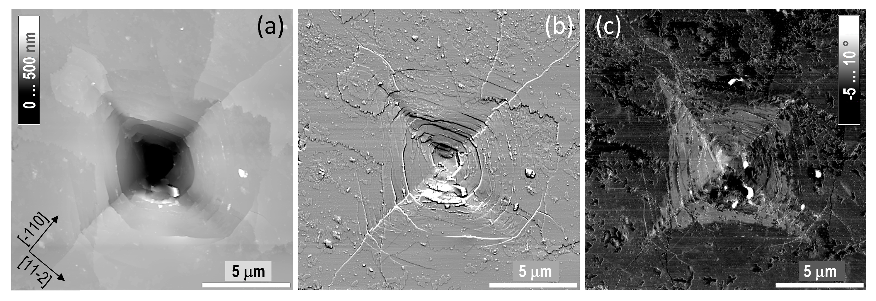
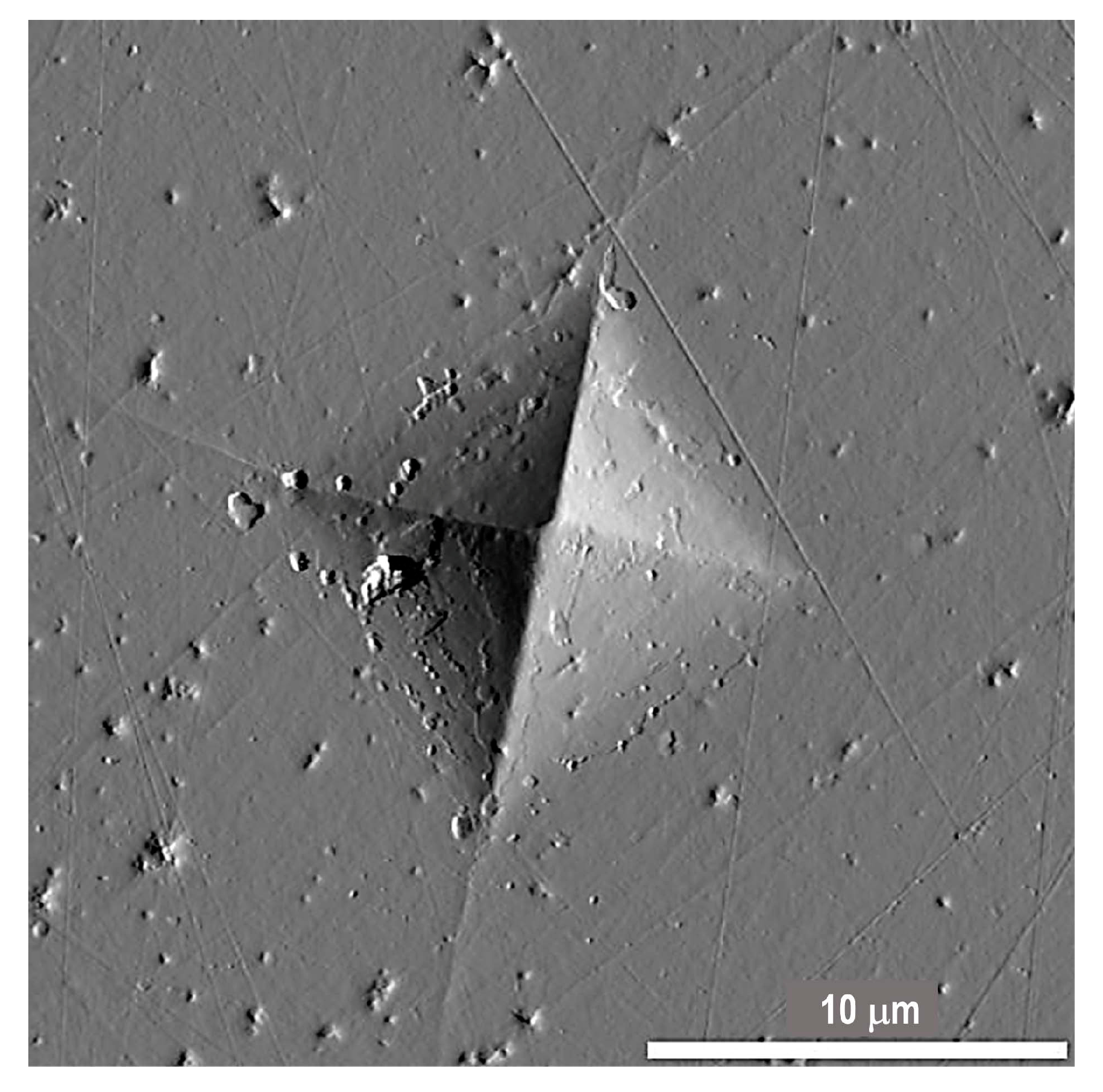
Figure 2 shows the AFM images of 4.91-N Vickers indents taken on the (111) face of synthetic Ib diamond. It can be seen from Figure 2a (topography) and Figure 2b (derivative topography) that the plasticity of the diamond is very low—there is a large number of a ring (Hertzian) cracks in the region of contact aligned along the <011> directions (Figure 2a,b). Additionally, long radial cracks emanate from the indent corners. According to Figure 2a,b a Vickers indent in diamond does not have sharp and clear boundaries and its hardness measurement is complicated. However, AFM in the phase contrast operation mode reveals the formation of a new viscoelastic phase in the contact (Figure 2c). It is known that micro-Raman spectroscopy reveals a disordered graphite in a Vickers indent in diamond [22,23]. A high pressure and high shear stress in the contact causes a phase transformation of diamond to graphite during hardness test. Probably, graphite in the indent was formed during unloading through unknown high pressure metallic phase of carbon [23] similar to that in silicon [31].
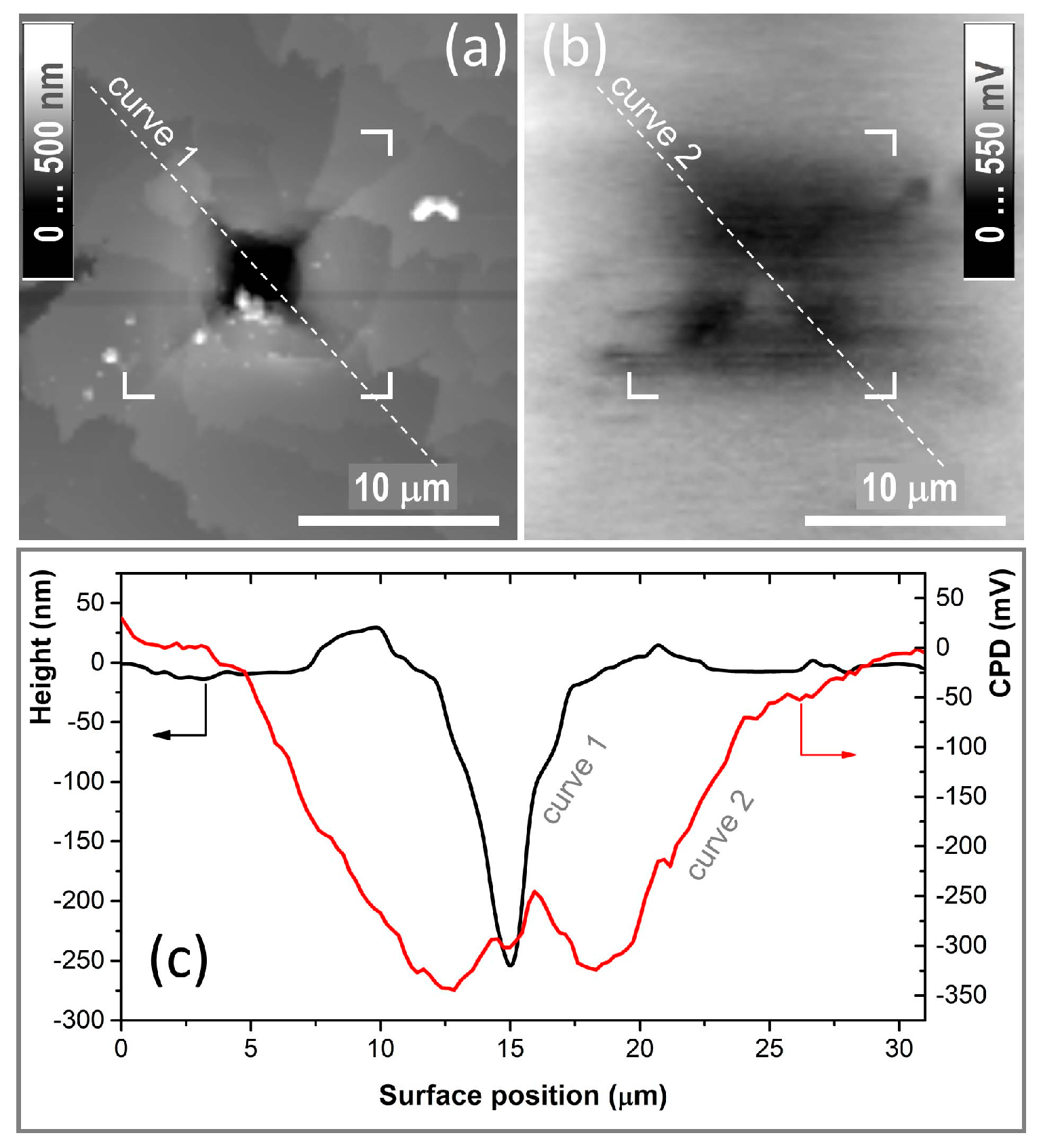
The KPFM measurements also detects a new phase in the vicinity of the indent through an electrostatic tip-surface interaction instead of mechanical one in the previous case. Figure 3 illustrates simultaneously-captured topography and contact potential difference (CPD) over the diamond surface with the Vickers indent. The work function of the diamond could be expected within 3.9–4.2 eV [32].
Taking into account the 5.0 eV work function of a thin carbon film [33] and the 5.5 eV of Pt/Ir tip, the lowering of CPD over the graphite phase in the indent should be observed (up to 0.8 eV in the ideal case). As it follows from CPD profiles (Figure 3c, curve 2) the real difference could reach a value of 350 mV. Thus, AFM and KPFM data allow us to suppose the viscoelastic phase in the region of the Vickers indent on diamond to be disordered graphite.
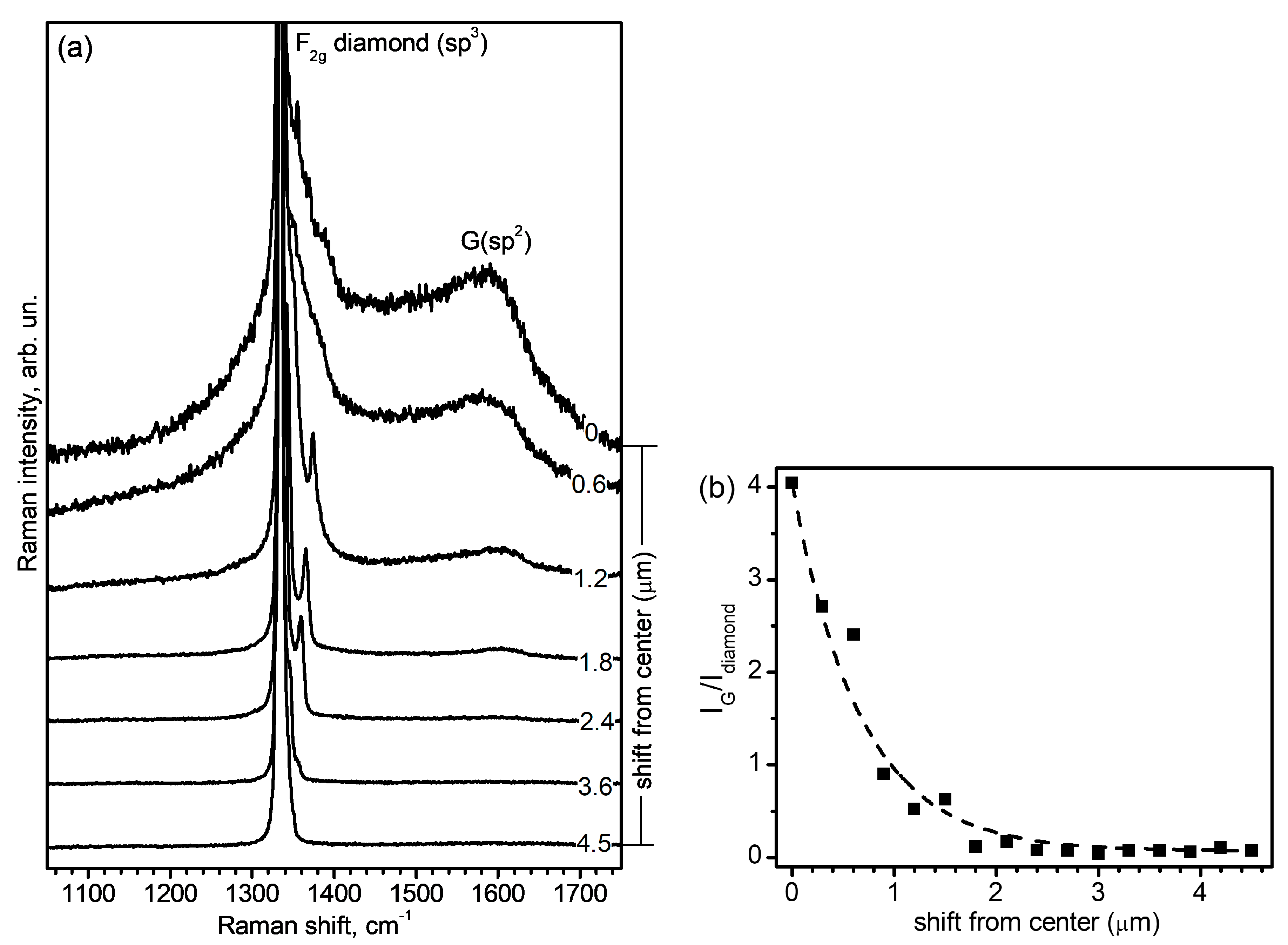
Confocal micro-Raman spectroscopy of the Vickers indent on the surface of (111) type-Ib synthetic diamond was applied to check the above mentioned assumption. Raman spectra taken in the indented area (Figure 4a) besides the main F2g diamond phonon band at ~1334 cm−1 also contain broadened bands at ~1350 and ~1580 cm−1, corresponding to the D and G bands of the sp2 amorphous carbon phase, which appears due to graphitization of diamond during indentation [23]. Scanning along the indent from its centre to edge (Figure 4а) revealed non-uniform spatial distribution of the sp2 carbon phase with its highest content in the centre of the indent and gradually decreasing to the edge, which is qualitatively demonstrated by the distribution of the relative intensity of the diamond F2g band to the intensity of the graphite G-band (Figure 4b).
It should be also noted that a series of narrow low-intensity bands with variable frequency positions were registered on the high-energy side of the diamond F2g peak in the range of 1335–1390 cm−1 (Figure 5a). The appearance of additional bands in the Raman spectra during indentation can be associated with the formation of metastable phases and, in particular, of the hexagonal diamond (lonsdaleite) phase [34], which was predicted theoretically [35]. However, the Raman spectrum of lonsdaleite is expected to contain phonon bands in the range of 1224–1242 cm−1, 1292–1303 cm−1, and 1338 cm−1 corresponding to E2G, A1g, and E1g vibrational modes [35,36]. Moreover, the A1g mode in the region of 1292–1303 cm−1 should be the most intense in the spectrum, which is not observed in our case. Thus, the additional bands registered in the range of 1335–1390 cm−1 cannot be attributed to lonsdaleite.
On the other hand, the appearance of additional bands in the Raman spectrum of diamond on the high-frequency side of the F2g band may be due to the presence of residual compressive strain that can remain in the indented area. Similar behaviour of the phonon band was observed earlier in the Raman spectra of diamond subjected to shock compressive deformations [37]. Thus, uniaxial or biaxial compressive strains can partially or completely remove the degeneracy of the triply-degenerate diamond F2g band with the corresponding splitting of diamond Raman peak into two or three components with a gradual high-frequency shift of the latter with strain [38].
Thus, the three registered bands in the range of 1335–1390 cm−1, which are denoted as ω1, ω2, and ω3 in Figure 5a,b in accordance with [38], can be presumably assigned to the components of the triplet, which is formed due to the splitting of the diamond F2g band (ω0) under uniaxial compressive strain. It should be noted that simultaneous registration in the spectrum of a more intense unsplit ω0 diamond band indicates that both strained and unstrained regions of the diamond coexist within the area of the Raman probe. For confocal scanning at a wavelength of λexc = 488.0 nm, the lateral resolution is defined by the lateral size of the focused laser beam waist, dlateral = 0.4λexc NA−1 ≈ 210 nm, and the axial resolution is defined by the axial waist size, Raxial = 1.4(λexcμ) (NA)−2 ≈ 1.8 μm.
The gradual low-frequency shift of ω1, ω2, and ω3 bands towards the diamond ω0 band is observed at scanning from the center of the indent to its edge (Figure 5c), which apparently corresponds to the gradual strain relaxation along the studied area. A rough estimate of the strain on the basis of the data of [38] and assuming uniaxial compression in the [110] direction gives a value of the order of 20 GPa. Additionally, the Raman spectra measured near the edge of the indent revealed a weak peak (ω4) with a frequency of about 1330 cm−1, i.e., lower than the diamond ω0 band, and which shifts slightly to the high-frequency region from 1330 to 1331 cm−1 when approaching the edge of the indent (Figure 6). This peak can tentatively be associated with the presence of a tensile strained diamond region near the edge of the indent, which appears due to the compressive strains inside the indent.
Thus, the new phase revealed by the AFM in the indent on the surface of diamond is graphite. Therefore, the phase-transformed contact area (60.05 × 10⁶ nm2) determined by the AFM in the phase contrast operation mode, was taken as the contact area and was used to determine the Vickers hardness of diamond.
3.2. AFM Imaging of Vickers Indents on (111) and (001) cBN Single Crystals
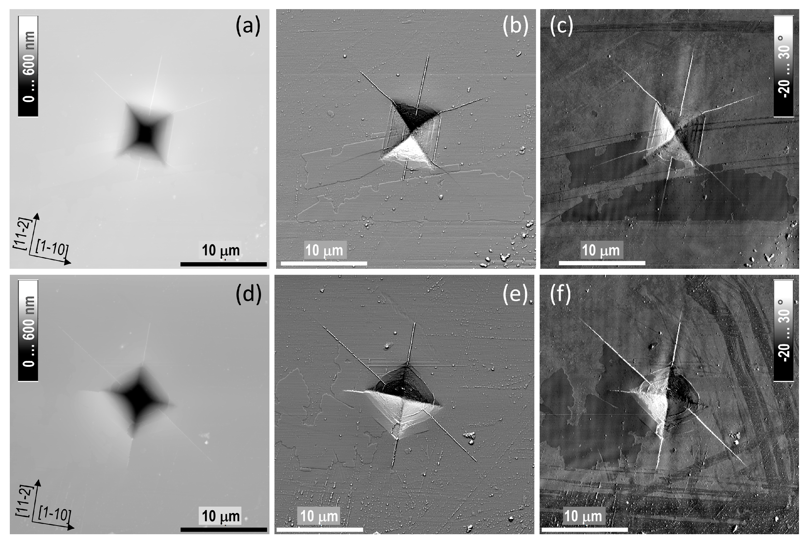
Figure 7 shows AFM images (1.96–N load) of A and B indents on the (111) plane of the cBN single crystals. The well-developed plastic indents are observed on the (111) plane. The shape of the Vickers indents are close to square. A long radial cracks are formed in the B indents (Figure 7a–c) on the {011}90° planes in the <112> directions. A short radial crack is formed along <110> direction for the A indent (Figure 7d–f) additionally to long radial cracks in <112> directions. It is well known that the {111} plane is the preferred cleavage plane of diamond. The crystalline lattice of cBN is the same as in diamond. Thus, the {111} cleavage should be expected for cBN. However, at the hardness testing of (111) cBN only {011}90° cleavage was observed (Figure 7). It should be noted that, for the cleavage, not only is the surface energy of the crystallographic plane important, but so too is its orientation relative to the plane being tested. For example, with the Vickers hardness test on the (001) surface of diamond the actual cleavage planes are {011}90° and {111}54°44′, in this case the {011}90° cleavage prevails [39]. Probably, the {111}90° cleavage planes in cBN are possible at the testing of the (011) plane as it occurs at testing the (011) plane of diamond [40].
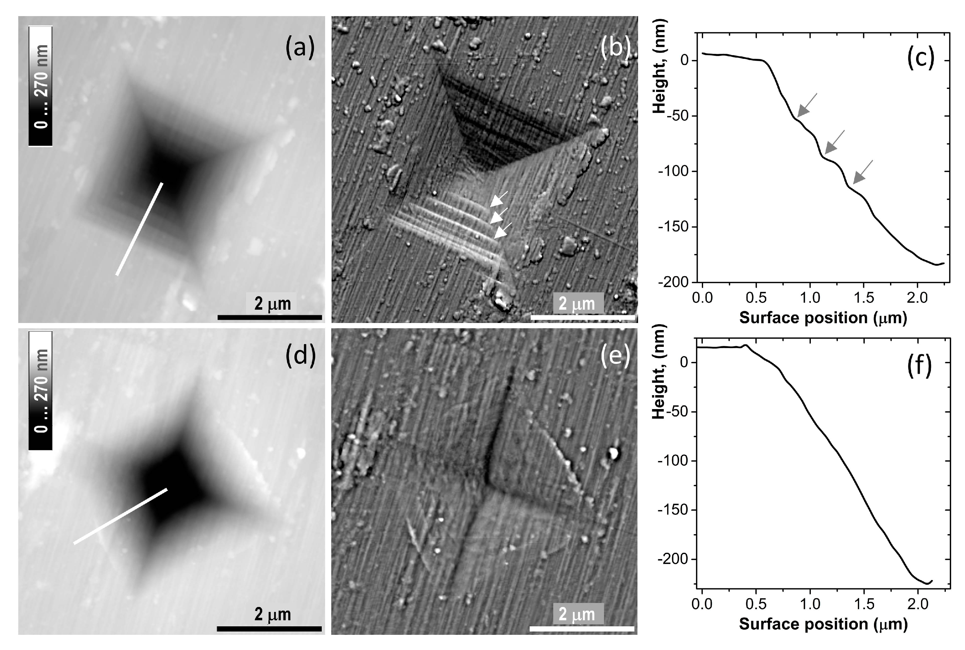
The AFM image of the 1.96-N load <110> indent on the (001) cBN plane in contrast to the (111) plane does not reveal radial cracks. Only the ring cracks are observed in these indents. This observation indicates a significant anisotropy of the fracture toughness in cBN single crystals. Especially interesting are the 0.49-N indents on the (001) cBN plane (Figure 8). The clear linear details along the <110> direction are observed in the <100> Vickers indent, which look like slip lines. Brookes et al. [41] annealed a room-temperature Knoop indent on the (001) plane of cBN at 900 °C and then etched the sample surface to reveal the slip lines around the indent. The orientation of the slip lines makes it possible to identify the active slip system in cBN. It was concluded that it is a {111} <110> slip system [41]. Thus, the <110> directions of the linear features in the <100> indent (Figure 8a–c) support the assumption that they are slip lines. However, further study is necessary to make a final decision. In any case, the AFM images of the Vickers indents on the (001) plane indicate unexpectedly high plasticity of cBN at room temperature as compared with diamond.
Figure 9 shows the AFM derivative topography of a 4.91-N indent on the surface of the nanopolycrystalline cBN compact. The ring cracks in the indent and around it are absent, only rather short radial cracks are observed. The shape of the indent is close to a square, and projected area of the indent is 81.40 × 10⁶ nm2.
3.3. Vickers Hardness and Fracture Toughness of Diamond and cBN Single Crystals
The Vickers hardness HV (GPa) is calculated as a ratio of the indentation load P (N) to the lateral indent surface using the standard equation for the Vickers geometry:
where d is the indent diagonal length (μm), and φi is the angle between opposite faces of the Vickers diamond indenter (136°). The following assumptions are made using this equation: (a) the shape of the indent is close to a square, and (b) the elastic deformation of a diamond indenter under the load is negligibly small (i.e., the indenter is rigid). Such assumptions are quite acceptable in hardness testing of soft and low-modulus materials. However, it is necessary to account for a change of the Vickers indenter geometry caused by the elastic deformation at the hardness testing of such high-modulus materials as diamond and cBN. We used a model proposed by B. Galanov et al. to account for the change of the Vickers indenter geometry due to elastic deformation [42]:
where φ is the angle between opposite faces of the Vickers diamond indenter under the load, HM is the Meyer hardness of the sample, and E* is the reduced modulus. The effect of hardness and elastic modulus of materials on the elastic deformation of the Vickers diamond indenter are given in the Table 1.
It can be seen from the table that the geometry of the Vickers indenter changes significantly during the penetration into the surface of hard and superhard materials. The φ/2 angle increases from 68° (initial shape) up to 77° (a penetration into the diamond surface). However, sin(φ/2) changes much less than the growth of the 2HM/E* ratio (Table 1). Therefore, accounting for the elastic deformation of the Vickers diamond indenter is important only for the hardest materials. An increase of the proportionality coefficient in Equation (2) does not exceed 5% for diamond and 3.4% for cBN.
Additionally, Equation (2) supposes that the Vickers indent has the shape of a square. This is a rather rare case. The sinking of the surface around the indent (concave shape) is observed for annealed metals and the real contact area is lower as compared with a square indent with the same diagonals [43]. The situation is contrary in the case of previously-deformed metals: the formation of pile up around the indent (convex shape) takes place and the real contact area is higher than that of a square. The equivalent diagonal of the indent deq (μm) was determined to account for real projected area of the indent in diamond using an equation that connects the area of square indent with the diagonal:
where A is the projected contact area (106 nm2) measured by AFM. For example, according to the AFM, the projected area of the Vickers indent on the surface of the (111) diamond at 5-N load is 60,044,943 nm2. From here, using Equation (4), we obtained that deq is 10.96 μm, whereas according to the AFM image (Figure 2c) the real length of diagonal is 13.06 μm. Substituting deq into Equation (2) and taking into account that 2sin(φ/2) for the diamond sample is 1.9501 (Table 1), we finally obtained that the Vickers hardness of type-Ib (111) synthetic diamond is 79.7 GPa (4.91-N load, Table 2). Due to the concave shape of an indent on the surface of diamond, the phase-transformed contact area determined by the AFM is smaller than the indented area defined by the diagonal’s length. Therefore, the HV values for diamond single crystals in the previous publications [39,40,44] can be underestimated.
The Vickers hardness of the (111) plane of type-Ib synthetic diamond at 5-N load is about 80 GPa, which is appreciably lower than the Vickers hardness of natural type-Ia diamond (92 GPa [12]). This is probably the consequence of a high density of dislocations and nitrogen concentration in the type-Ib synthetic diamond sample produced by the spontaneous crystallization. This value (80 GPa) is higher than the Vickers hardness of the (011) natural diamond after etching of the indent in the KNO3 melt (67 GPa without account for elastic deformation of Vickers indenter [45]). However, it is appreciably lower than was determined using optical microscopy for measuring the as-received indent in the (111) and (001) diamond single crystals (about 100–115 GPa for both planes [39,44]). The Vickers hardness of the (111) cBN single crystals (1.96-N load) is approximately the same for both orientations of indents on the (111) plane ~49 GPa. It is much less than the HV of the (111) cBN data, according to the optical microscopy (62 GPa [46]). Probably, the spatial resolution of the optical microscopy is not high enough for reliable measurements of indents in diamond and cBN single crystals, especially at low applied loads. The Vickers hardness of nanopolycrystalline cBN is about 60 GPa (5-N load), which is much higher than for the (111) cBN single crystal (49 GPa, 1.96 N). A random orientation of the grains in a nanopolycrystalline sample suppresses the perfect cleavage of cBN on the {110} planes. Therefore, the fracture toughness of nanopolycrystalline cBN is also higher than for cBN single crystals, i.e., 7.9 MPa m0.5 and 3.2 MPa m0.5, respectively (Table 2). It follows from the tests results that grains and nanotwin boundaries in nanopolycrystalline cBN cause an increase not only in the hardness, but in the fracture toughness of materials as well.
At the present time, the ratio of the indentation load to the projected contact area is often used for hardness determination, for example, in nanoindentation. It is a Meyer hardness HM. The elastic deformation of the indenter does not affect the projected contact area. Since the area of pyramid base is lower than its lateral surface, the HM is higher than HV. In the case of the rigid Vickers indenter, the HM to HV ratio is 1.078. The Meyer hardness for diamond and cBN samples is given in Table 2.
4. Conclusions
Vickers hardness of the (111) synthetic type 1b diamond, (001) and (111) cBN single crystals, and a nanopolycrystalline cBN bulk sample was studied in this paper. Atomic force microscopy in the phase contrast operation mode, micro-Raman spectroscopy, and Kelvin probe force microscopy were used for accurate identifying the projected contact area of Vickers indents on the surface of diamond. The effect of the elastic deformation of the diamond Vickers indenter on its geometry was accounted for at the hardness measurements. It was shown that:
1. The Vickers hardness of the (111) plane of type-Ib synthetic diamond at 5-N load is about 80 GPa, which is appreciably lower than the Vickers hardness of natural-type-Ia diamond (92 GPa [12]). Probably, this is a consequence of a high density of dislocations and nitrogen concentration in the type-Ib synthetic diamond sample produced by the spontaneous crystallization.
2. The Vickers hardness of the (111) cBN single crystal at 2-N load is about 49 GPa. The appreciable anisotropy of Vickers hardness is observed on the (001) plane of cBN.
3. Grains and nanotwin boundaries in the nanopolycrystalline cBN sample resulted in the enhancement of both the Vickers hardness and fracture toughness as compared with cBN single crystals.
4. The determination of the Vickers hardness of diamond by the indent diagonals length results in the underestimated value as the concave shape of the contact under load is not taken into account.
Author Contributions
Sergey Dub, Petro Lytvyn and Viktor Strelchuk conceived the project. Igor Petrusha, Takashi Taniguchi and Sergey Ivakhnenko performed the HPHT experiments. Sergey Dub performed the hardness measurements. Viktor Strelchuk, Andrii Nikolenko and Yurii Stubrov performed the micro-Raman spectroscopy and analyzed the data. Petro Lytvyn performed the atomic force microscopy. Sergey Dub, Petro Lytvyn and Andrii Nikolenko wrote the paper. All authors discussed the results and commented on the manuscript.
Conflicts of Interest
The authors declare no conflict of interest.
References
- Chowdhury, S.; de Barra, E.; Laugier, M.T. Hardness measurement of CVD diamond coatings on SiC substrates. Surf. Coat. Technol. 2005, 193, 200–205. [Google Scholar] [CrossRef]
- Irifune, T.; Kurio, A.; Sakamoto, S.; Inoue, T.; Sumiya, H. Materials: Ultrahard polycrystalline diamond from graphite. Nature 2003, 421, 599–600. [Google Scholar] [CrossRef] [PubMed]
- Sumiya, H.; Irifune, T. Indentation hardness of nano-polycrystalline diamond prepared from graphite by direct conversion. Diam. Relat. Mater. 2004, 13, 1771–1776. [Google Scholar] [CrossRef]
- Sumiya, H.; Uesaka, S.; Satoh, S. Mechanical properties of high purity polycrystalline cBN synthesized by direct conversion sintering method. J. Mater. Sci. 2000, 35, 1181–1186. [Google Scholar] [CrossRef]
- Huang, Q.; Yu, D.; Xu, B.; Hu, W.; Ma, Y.; Wang, Y.; Zhao, Z.; Wen, B.; He, J.; Liu, Z.; et al. Nanotwinned diamond with unprecedented hardness and stability. Nature 2013, 510, 250–253. [Google Scholar] [CrossRef] [PubMed]
- Dubrovinskaia, N.; Solozhenko, V.L.; Miyajima, N.; Dmitriev, V.; Kurakevych, O.O.; Dubrovinsky, L. Superhard nanocomposite of dense polymorphs of boron nitride: Noncarbon material has reached diamond hardness. Appl. Phys. Lett. 2007, 90, 101912. [Google Scholar] [CrossRef]
- Solozhenko, V.L.; Kurakevych, O.O.; Le Godec, Y. Creation of nanostuctures by extreme conditions: High-pressure synthesis of ultrahard nanocrystalline cubic boron nitride. Adv. Mater. 2012, 24, 1540–1544. [Google Scholar] [CrossRef] [PubMed]
- Tian, Y.; Xu, B.; Yu, D.; Ma, Y.; Wang, Y.; Jiang, Y.; Hu, W.; Tang, C.; Gao, Y.; Luo, K.; et al. Ultrahard nanotwinned cubic boron nitride. Nature 2013, 493, 385–388. [Google Scholar] [CrossRef] [PubMed]
- Nagakubo, A.; Ogi, H.; Sumiya, H.; Hirao, M. Elasticity and hardness of nano-polycrystalline boron nitrides: The apparent Hall-Petch effect. Appl. Phys. Lett. 2014, 105, 081906. [Google Scholar] [CrossRef]
- Liu, X.; Chang, Y.-Y.; Tkachev, S.N.; Bina, C.R.; Jacobsen, S.D. Elastic and mechanical softening in boron-doped diamond. Sci. Rep. 2017, 7, 42921. [Google Scholar] [CrossRef] [PubMed]
- Sumiya, H.; Ishida, Y.; Arimoto, K.; Harano, K. Real indentation hardness of nano-polycrystalline cBN synthesized by direct conversion sintering under HPHT. Diam. Relat. Mater. 2014, 48, 47–51. [Google Scholar] [CrossRef]
- Xu, B.; Tian, Y. Ultrahardness: Measurement and enhancement. J. Phys. Chem. C 2015, 119, 5633–5638. [Google Scholar] [CrossRef]
- Drory, M.D.; Dauskardt, R.H.; Kant, A.; Ritchie, R.O. Fracture of synthetic diamond. J. Appl. Phys. 1995, 78, 3083–3088. [Google Scholar] [CrossRef]
- Solozhenko, V.L.; Dub, S.N.; Novikov, N.V. Mechanical properties of cubic BC2N, a new superhard phase. Diam. Relat. Mater. 2001, 10, 2228–2231. [Google Scholar] [CrossRef]
- Zerr, A.; Kempf, M.; Schwarz, M.; Kroke, E.; Göken, M.; Riedel, R. Elastic moduli and hardness of cubic silicon nitride. J. Am. Ceram. Soc. 2002, 85, 86–90. [Google Scholar] [CrossRef]
- Dub, S.N.; Petrusha, I.A. Mechanical properties of polycrystalline cBN obtained from pyrolytic gBN by direct transformation technique. High Press. Res. 2006, 26, 71–77. [Google Scholar] [CrossRef]
- Dub, S.N.; Petrusha, I.A.; Bushlya, V.M.; Taniguchi, T.; Belous, V.A.; Tolmachova, G.N.; Andreev, A.V. Theoretical shear strength and the onset of plasticity in nanodeformation of cubic boron nitride. J. Superhard Mater. 2017, 39, 88–98. [Google Scholar] [CrossRef]
- Richter, A.; Ries, R.; Smith, R.; Henkel, M.; Wolf, B. Nanoindentation of diamond, graphite and fullerene films. Diam. Relat. Mater. 2000, 9, 170–184. [Google Scholar] [CrossRef]
- Sawa, T.; Tanaka, K. Nanoindentation of natural diamond. Philos. Mag. A 2002, 82, 1851–1856. [Google Scholar] [CrossRef]
- Dubrovinskaia, N.; Dub, S.; Dubrovinsky, L. Superior wear resistance of aggregated diamond nanorods. Nano Lett. 2006, 6, 824–826. [Google Scholar] [CrossRef] [PubMed]
- Dub, S.N.; Brazhkin, V.V.; Belous, V.A.; Tolmacheva, G.N.; Konevskii, P.V. Comparative nanoindentation of single crystals of hard and superhard oxides. J. Superhard Mater. 2014, 36, 217–230. [Google Scholar] [CrossRef]
- Gogotsi, Y.G.; Kailer, A.; Nickel, K.G. Pressure-induced phase transformations in diamond. J. Appl. Phys. 1998, 84, 1299–1304. [Google Scholar] [CrossRef]
- Gogotsi, Y.G.; Kailer, A.; Nickel, K.G. Transformation of diamond to graphite. Nature 1999, 401, 663–664. [Google Scholar] [CrossRef]
- Suprun, O.M.; Ilnitskaya, G.D.; Kalenchuk, V.A.; Zanevskii, O.A.; Shevchuk, S.N.; Lysakovskii, V.V. Change of dislocations density in single crystals of various types diamonds depending on the growth temperature and rate. Funct. Mater. 2016, 23, 552–556. [Google Scholar] [CrossRef]
- Khvostantsev, L.G.; Slesarev, V.N. Large-volume high-pressure devices for physical investigations. UFN 2008, 51, 1059–1063. [Google Scholar] [CrossRef]
- Anstis, G.R.; Chantikul, P.; Lawn, B.R.; Marshal, D.B. A critical evaluation of indentation techniques for measuring fracture toughness: I, direct crack measurements. J. Am. Ceram. Soc. 1981, 64, 533–538. [Google Scholar] [CrossRef]
- Zhong, Q.; Inniss, D.; Kjoller, K.; Elings, V.B. Fractured polymer/silica fiber surface studied by tapping mode atomic force microscopy. Surf. Sci. 1993, 290, L688–L692. [Google Scholar] [CrossRef]
- Radmacher, M.; Tillmann, R.W.; Gaub, H.E. Imaging viscoelasticity by force modulation with the atomic force microscope. Biophys. J. 1993, 64, 735–742. [Google Scholar] [CrossRef]
- Magonov, S.N.; Elings, V.; Whangbo, M.-H. Phase imaging and stiffness in tapping-mode atomic force microscopy. Surf. Sci. 1997, 375, L385–L391. [Google Scholar] [CrossRef]
- Nonnenmacher, M.; O’Boyle, M.P.; Wickramasinghe, H.K. Kelvin probe force microscopy. Appl. Phys. Lett. 1991, 58, 2921–2923. [Google Scholar] [CrossRef]
- Domnich, V.; Gogotsi, Y.; Dub, S. Effect of phase transformations on the shape of unloading curve in the nanoindentation of silicon. Appl. Phys. Lett. 2000, 76, 2214–2216. [Google Scholar] [CrossRef]
- Diederich, L.; Küttel, O.M.; Aebi, P.; Schlapbach, L. Electron affinity and work function of differently oriented and doped diamond surfaces determined by photoelectron spectroscopy. Surf. Sci. 1998, 418, 219–239. [Google Scholar] [CrossRef]
- Robrieux, B.; Faure, R.; Dussaulcy, J.P. Resistivity and electronic work function of very thin film carbon. C. R. Acad. Sci. Ser. B 1974, 278, 659–662. [Google Scholar]
- Xu, C.; Liu, C.; Wang, H. Incipient plasticity of diamond during nanoindentation. RSC Adv. 2017, 7, 36093–36100. [Google Scholar] [CrossRef]
- Denisov, V.N.; Mavrin, B.N.; Serebryanaya, N.R.; Dubitsky, G.A.; Aksenenkov, V.V.; Kirichenko, A.N.; Kuzmin, N.V.; Kulnitskiy, B.A.; Perezhogin, I.A.; Blank, V.D. First-principles, UV Raman, X-ray diffraction and TEM study of the structure and lattice dynamics of the diamond—Lonsdaleite system. Diam. Relat. Mater. 2011, 20, 951–953. [Google Scholar] [CrossRef]
- Goryainov, S.V.; Likhacheva, A.Y.; Rashchenko, S.V.; Shubin, A.S.; Afanas’ev, V.P.; Pokhilenko, N.P. Raman identification of lonsdaleite in Popigai impactites. J. Raman Spectrosc. 2014, 45, 305–313. [Google Scholar] [CrossRef]
- Boteler, J.M.; Gupta, Y.M. Shock induced splitting of the triply degenerate Raman line in diamond. Phys. Rev. Lett. 1993, 71, 3497. [Google Scholar] [CrossRef] [PubMed]
- Boteler, J.M.; Gupta, Y.M. Raman spectra of shocked diamond single crystals. Phys. Rev. B 2002, 66, 014107. [Google Scholar] [CrossRef]
- Novikov, N.V.; Dub, S.N. Fracture toughness of diamond single crystals. J. Hard Mater. 1991, 2, 3–11. [Google Scholar]
- Novikov, N.V.; Dub, S.N.; Mal’nev, V.I.; Beskrovanov, V.V. Mechanical properties of diamond at 1200 °C. Diam. Relat. Mater. 1994, 3, 198–204. [Google Scholar] [CrossRef]
- Brookes, C.A.; Hooper, R.M.; Lambert, W.A. Identification of slip systems in cubic boron nitride. Philos. Mag. A 1983, 47, L.9–L.12. [Google Scholar] [CrossRef]
- Galanov, B.A.; Milman, Y.V.; Chugunova, S.I.; Goncharova, I.V. Investigation of mechanical properties of high-hardness materials by indentation. J. Superhard Mater. 1999, 21, 23–35. [Google Scholar]
- Lim, Y.Y.; Chaudhri, M.M. The effect of the indenter load on the nanohardness of ductile metals: An experimental study on polycrystalline work-hardened and annealed oxygen-free copper. Philos. Mag. A 1999, 79, 2979–3000. [Google Scholar] [CrossRef]
- Dub, S.N. Fracture Toughness Determination of Superhard Single Crystals by Indentation. Ph.D. Thesis, Institute for Superhard Materials of the Academy of Sciences of Ukraine, Kiev, Ukraine, 1 November 1984. [Google Scholar]
- Novikov, N.V.; Dub, S.N. Hardness and fracture toughness of CVD diamond film. Diam. Relat. Mater. 1996, 5, 1026–1030. [Google Scholar] [CrossRef]
- Novikov, N.V.; Dub, S.N.; Malnev, V.I. Microhardness and fracture toughness of cubic boron nitride single crystals. Sov. J. Superhard Mater. 1983, 5, 16–20. [Google Scholar]
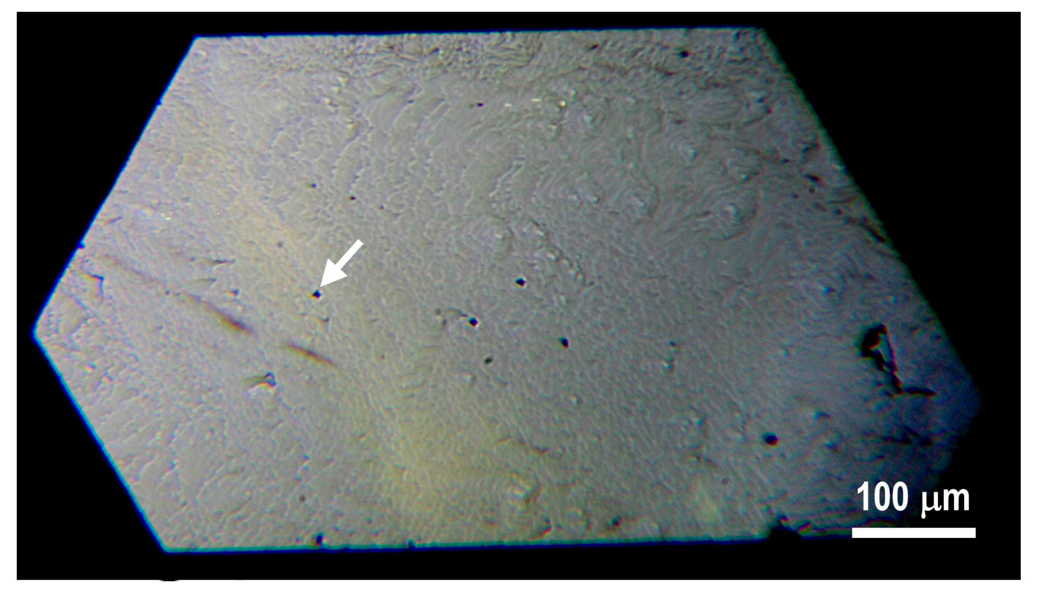
Figure 1.
(111) plane of the synthetic diamond single crystal. The arrow points to the indent which was studied by AFM and micro-Raman techniques.
Figure 1.
(111) plane of the synthetic diamond single crystal. The arrow points to the indent which was studied by AFM and micro-Raman techniques.

Figure 2.
AFM images of a Vickers indent (5-N load) on the (111) synthetic diamond: (a) topography; (b) derivative topography; and (c) phase contrast.
Figure 2.
AFM images of a Vickers indent (5-N load) on the (111) synthetic diamond: (a) topography; (b) derivative topography; and (c) phase contrast.

Figure 3.
(a) Topography and (b) corresponding tip-surface CPD maps for the indent in diamond shown in Figure 1. (c) Cross-sections of maps along the same line on surface: relief profile (curve 1) and CPD profile (curve 2). Corner-like marks are shown to compare areas of low CPD and the indent area.

Figure 4.
(a) Set of Raman spectra and (b) IG/Idiamond intensity ratio obtained by lateral scanning across the Vickers indent in diamond from its center to edge. The dashed line is shown to guide the eye.
Figure 4.
(a) Set of Raman spectra and (b) IG/Idiamond intensity ratio obtained by lateral scanning across the Vickers indent in diamond from its center to edge. The dashed line is shown to guide the eye.

Figure 5.
(a) Set of Raman spectra obtained by lateral scanning across the indent in the diamond from centre to edge; (b) Example of decomposition of typical Raman spectra taken inside the indent; (c) Frequencies of Raman modes in dependence on the spatial position from the centre of the indent.
Figure 5.
(a) Set of Raman spectra obtained by lateral scanning across the indent in the diamond from centre to edge; (b) Example of decomposition of typical Raman spectra taken inside the indent; (c) Frequencies of Raman modes in dependence on the spatial position from the centre of the indent.
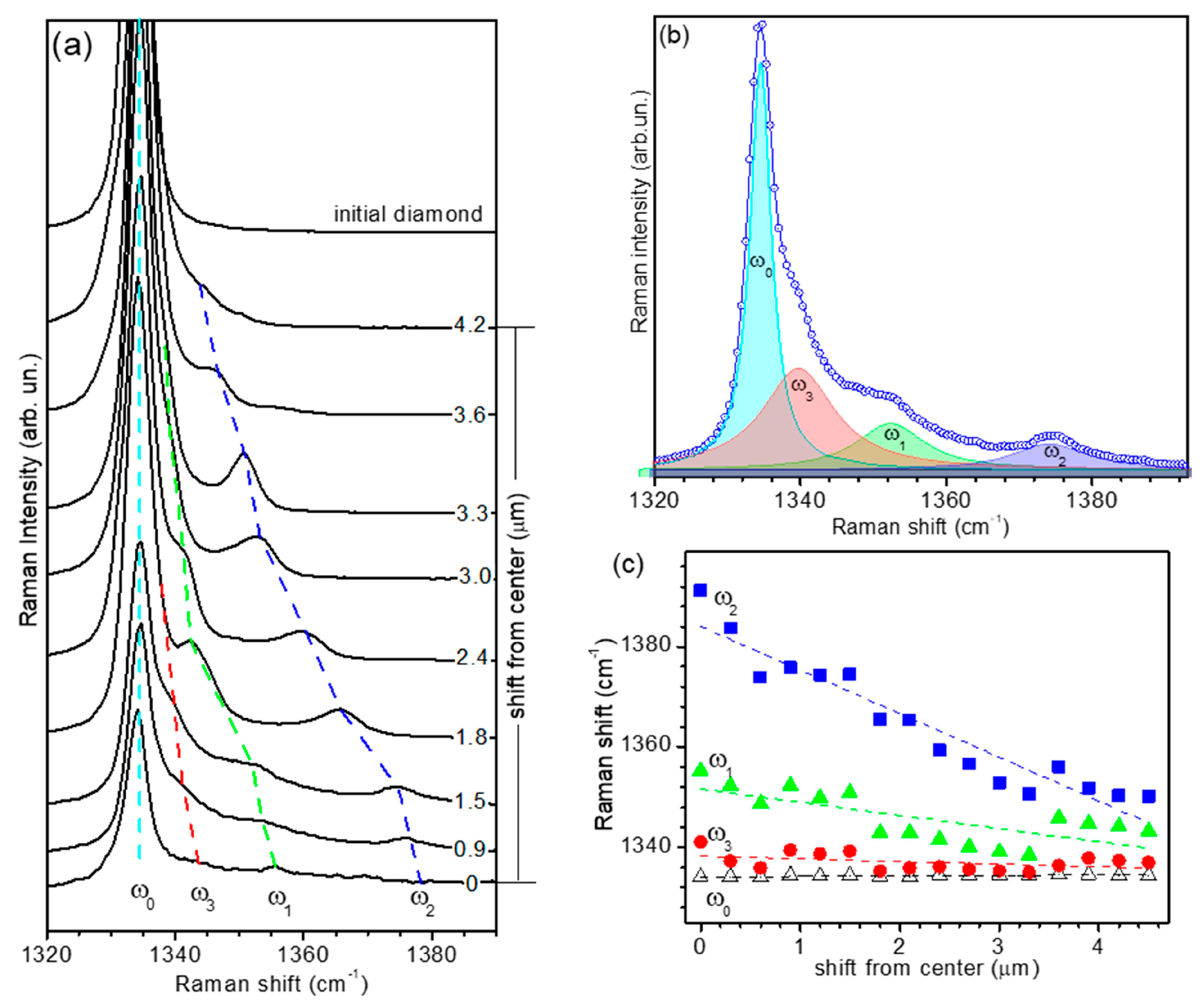
Figure 6.
Example of decomposition of the Raman spectra taken near the outer edge of the Vickers indent in (111) synthetic diamond single crystal.
Figure 6.
Example of decomposition of the Raman spectra taken near the outer edge of the Vickers indent in (111) synthetic diamond single crystal.
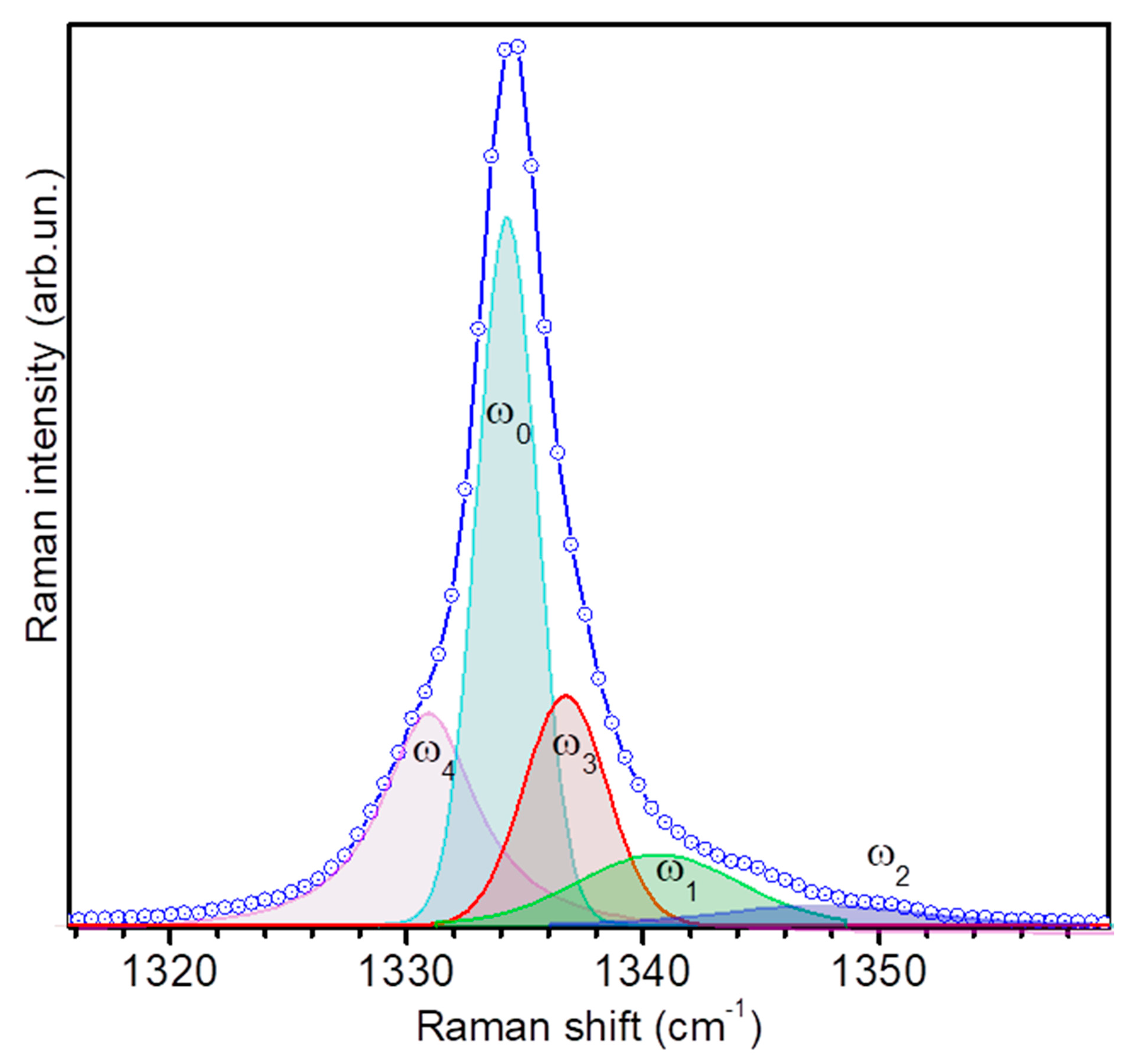
Figure 7.
(a–c) AFM images of orientations B and (d–f) orientation A of Vickers indents on the (111) cBN (1.96-N load): (a,d) topography, (b,e) derivative topography, and (c,f) phase contrast.
Figure 7.
(a–c) AFM images of orientations B and (d–f) orientation A of Vickers indents on the (111) cBN (1.96-N load): (a,d) topography, (b,e) derivative topography, and (c,f) phase contrast.

Figure 8.
(a–c) AFM images of <100> indent and (d–f) <110> indent on (100) cBN plane (0.49-N load): AFM topography (a,d) and derivative topography (b,e) images; and cross-section of indents (c,f) along the line shown in (a,d). Arrows indicate pronounced steps in the <100> indent aligned to <110> direction (b).

Figure 9.
AFM derivative topography image of Vickers indent on nanocrystalline cBN. 4.91-N load.


Table 1.
The effect of elastic deformation of Vickers indenter on its geometry for some materials.
| Sample | E, GPa | Poisson’s Ratio | HM, GPa | φ/2, ° | 2sin(φ/2) |
|---|---|---|---|---|---|
| Al | 72 | 0.35 | 0.36 | 68.04 | 1.8549 |
| SiO2 | 71 | 0.17 | 9 | 68.79 | 1.8646 |
| Al2O3 | 400 | 0.22 | 22 | 69.94 | 1.8787 |
| cBN | 850 | 0.12 | 62 | 73.58 | 1.9184 |
| Diamond | 1136 | 0.07 | 100 | 77.17 | 1.9501 |
Table 2.
Vickers and Meyer hardness of diamond and cBN measured taking into account the elastic deformation of the Vickers diamond indenter and the concave shape of indents.
Table 2.
Vickers and Meyer hardness of diamond and cBN measured taking into account the elastic deformation of the Vickers diamond indenter and the concave shape of indents.
| Sample | Load P, N | Projected Contact Area A, 106 nm2 | Equivalent Diagonal deq, μm | Vickers Hardness HV, GPa | Meyer Hardness HM, GPa | Radial Crack Length C, μm | Fracture Toughness KIC, MPa m0.5 |
|---|---|---|---|---|---|---|---|
| (111) Synthetic diamond | 4.91 | 60.05 | 10.96 | 79.7 | 81.7 | 14.2 [44] | 5.6 |
| Nano cBN compact | 4.91 | 81.40 | 12.51 | 60.2 | 61.5 | 11.40 | 7.9 |
| (111) cBN orientation A | 1.96 | 38.46 | 8.77 | 48.9. | 51.0 | 10.65 | 3.2 |
| (111) cBN orientation B | 1.96 | 39.05 | 8.84 | 48.2 | 50.2 | 11.37 | 3.5 |
| (001) cBN, orientation <100> | 1.96 | 38.04 | 8.72 | 49.4 | 51.5 | - | - |
| (001) cBN, orientation <110> | 1.96 | 43.36 | 9.31 | 43.4 | 45.2 | - | - |
© 2017 by the authors. Licensee MDPI, Basel, Switzerland. This article is an open access article distributed under the terms and conditions of the Creative Commons Attribution (CC BY) license (http://creativecommons.org/licenses/by/4.0/).
Share and Cite
MDPI and ACS Style
Dub, S.; Lytvyn, P.; Strelchuk, V.; Nikolenko, A.; Stubrov, Y.; Petrusha, I.; Taniguchi, T.; Ivakhnenko, S. Vickers Hardness of Diamond and cBN Single Crystals: AFM Approach. Crystals 2017, 7, 369. https://doi.org/10.3390/cryst7120369
AMA Style
Dub S, Lytvyn P, Strelchuk V, Nikolenko A, Stubrov Y, Petrusha I, Taniguchi T, Ivakhnenko S. Vickers Hardness of Diamond and cBN Single Crystals: AFM Approach. Crystals. 2017; 7(12):369. https://doi.org/10.3390/cryst7120369
Chicago/Turabian StyleDub, Sergey, Petro Lytvyn, Viktor Strelchuk, Andrii Nikolenko, Yurii Stubrov, Igor Petrusha, Takashi Taniguchi, and Sergey Ivakhnenko. 2017. "Vickers Hardness of Diamond and cBN Single Crystals: AFM Approach" Crystals 7, no. 12: 369. https://doi.org/10.3390/cryst7120369
Note that from the first issue of 2016, this journal uses article numbers instead of page numbers. See further details here.