
Thermal Stability of Epitaxial Graphene Electrodes for Conductive Polymer Nanofiber Devices
by
Kyung Ho Kim
1,*, 
Samuel Lara-Avila
1,2,
Hans He
1,
Hojin Kang
3,
Yung Woo Park
4,*,
Rositsa Yakimova
5 and
Sergey Kubatkin
1 1
Department of Microtechnology and Nanoscience, Chalmers University of Technology, Gothenburg SE412-96, Sweden
2
National Physical Laboratory, Hampton Road, Teddington TW11 0LW, UK
3
Department of Physics and Astronomy, Seoul National University, Seoul 08826, Korea
4
Institute of Applied Physics, Seoul National University, Seoul 08826, Korea
5
Department of Physics, Chemistry and Biology, Linkoping University, Linkoping SE581-83, Sweden
*
Authors to whom correspondence should be addressed.
Crystals 2017, 7(12), 378; https://doi.org/10.3390/cryst7120378
Submission received: 21 November 2017
/
Revised: 5 December 2017
/
Accepted: 11 December 2017
/
Published: 14 December 2017
(This article belongs to the Special Issue Integration of 2D Materials for Electronics Applications)
Abstract
:We used large area, monolayer graphene epitaxially grown on SiC (0001) as contact electrodes for polymer nanofiber devices. Our fabrication process, which avoids polymer resist residues on the graphene surface, results in graphene-polyaniline nanofiber devices with Ohmic contacts and electrical conductivity comparable to that of Au-nanofiber devices. We further checked the thermal stability of the graphene contacts to polyaniline devices by annealing up to T = 800 °C, the temperature at which polyaniline nanofibers are carbonized but the graphene electrode remains intact. The thermal stability and Ohmic contact of polymer nanofibers are demonstrated here, which together with the chemical stability and atomic flatness of graphene, make epitaxial graphene on SiC an attractive contact material for future all-carbon electronic devices.
1. Introduction
Conductive polymers are promising platforms for the next generation of carbon-based electronics. With these organic materials, the variety of devices that have already been developed span a wide range of applications that include flexible field–effect transistors [1], actuators [2], sensors [3], and nano-optoelectronic devices [4]. For conductive polymers, efficient injection and extraction of charges between the contact electrode and the active channel is often complicated due to the incompatibility between organic channels and inorganic contacts [5,6]. In this sense, carbon-based contacts [5], and particularly graphene, are appealing solutions to interface organic polymers to the outer world and materialize the vision of all-carbon electronics [5,7]. As an electrical contact, graphene offers numerous properties that complement the versatility of electronic polymers, including high electron mobility [8,9,10,11], thermal conductivity [12], optical transparency [13,14], tunability of work function [15], and chemical/thermal stability. Furthermore, in combination with metals, graphene could be also used as an interfacial layer to engineer the charge transfer between metal contacts and other carbon-based systems [16]. More generally, graphene as an electrical contact has been proven to be a superior solution in various electronics applications from organic field effect transistors [17,18,19,20,21,22,23], organic solar cells [24], organic light emitting diodes [25] to nanoelectromechanical infrared detectors [26], and electrophysiology and neuroimaging [27,28]. In addition to electronics, biosensors [29] and biomedical applications such as point-of-care testing devices [30] use graphene to improve analytical performances.
In practice, additional requirements that have to be met by graphene contact technologies include scalability, reproducibility (e.g., clean surface), and robustness against chemical and thermal treatments during device fabrication. Graphene grown by chemical vapor deposition (CVD) [16,17,18,19,25,26,27,28,31] and from reduced graphene oxide [24] are somewhat suitable for scalability. CVD graphene has to be transferred to an insulating substrate and the transfer process is prone to leave resist residues and to result in discontinuous graphene layers (i.e., voids) over large scales. An alternative technology is epitaxial graphene grown on the Si face of silicon carbide substrates (G/SiC), which has drawn less attention for contact technology due to the relative higher cost of materials. Nonetheless, as-grown G/SiC is also scalable [32], being a continuous single crystal with its size limited only by the SiC substrate size [33]. Additionally, G/SiC is atomically flat and clean implying that atomically clean interfaces can be readily achieved on this material. Since the SiC substrate is electrically insulating, there is no need to transfer (i.e., contaminate) the graphene layer. The main source of contamination for G/SiC is the microfabrication process that involves organic polymer resists. However, polymer residues can be avoided by using shadow masks or metal masks directly deposited on graphene during fabrication [34,35,36,37]. Alternatively, resist residues and other common contaminants of the surface can be removed using scalable methods such as high temperature annealing [38].
In this paper, we demonstrate the suitability of G/SiC as an electrical contact for polymer nanofibers, a low dimensional carbon system. We patterned a large area of G/SiC using a metal protection mask to ensure that the G/SiC surface is free of resist residues that degrade the nanofiber/graphene interface. For the organic channel, polyaniline (PANI) nanofibers were contacted on G/SiC and we found that the quality of contact is comparable to that of Au electrodes. We further checked the thermal stability of the device by annealing it at 800 °C under argon flow and upon annealing, we found that the graphene electrodes remained operational and the PANI nanofibers were carbonized as confirmed by current-voltage (I-V) characterization and Raman spectroscopy.
2. Results and Discussion
2.1. Characterization of Graphene Electrodes
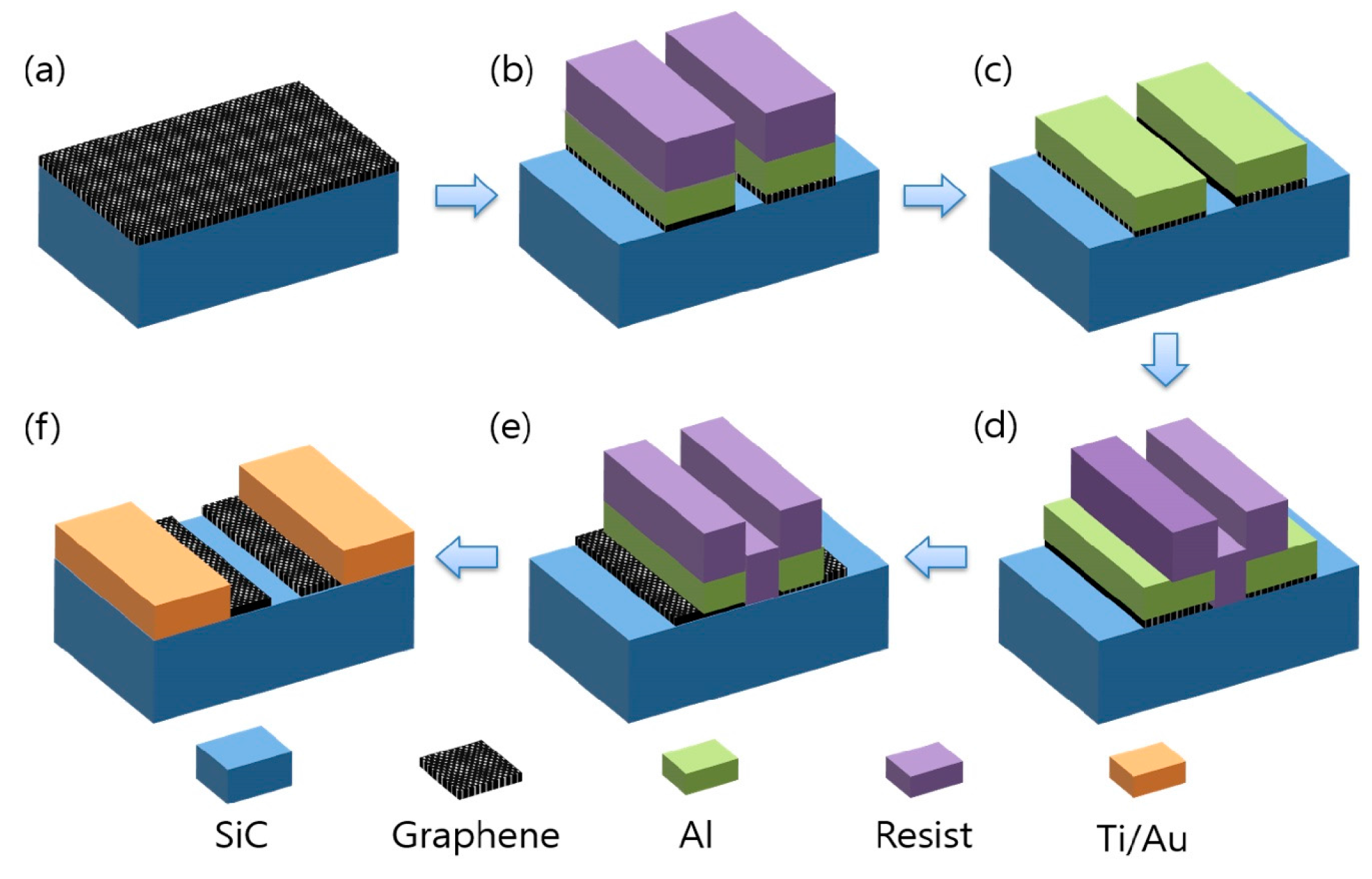
The as-grown G/SiC, characterized by the express optical microscopy method [39], is homogeneous monolayer graphene with about 10–15% bilayer domain inclusions [32]. Figure 1 is the schematic illustration of the fabrication process of the G/SiC electrode (see Methods), where the key step is the deposition of an aluminum protection layer on the as-grown material. This Al layer is removed in the last fabrication process, and its role is to prevent graphene from directly contacting organic resist that degrades the graphene-nanofiber interface. Together with G/SiC electrodes, we have fabricated Hall bars to enable the electrical characterization of the graphene layer. Hall measurement of the G/SiC shows that the electron mobility is of the order of ~1000 cm2/Vs and the electron carrier density is ~4 × 1012 cm−2 at 300 K. The high electron concentration is consistent with the charge transfer from the surface donor state of SiC to G/SiC reported previously [40,41].
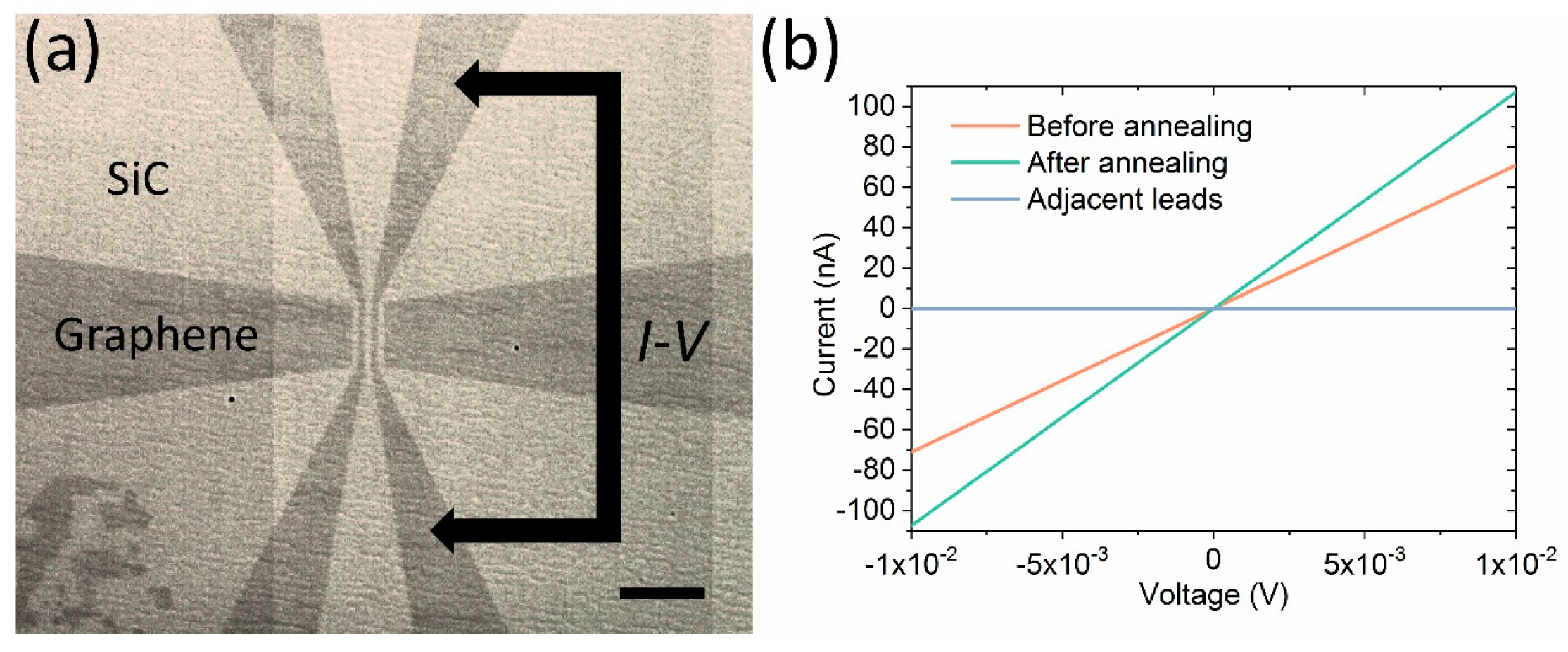
Figure 2a is the optical microscope image of a graphene electrode pattern with a length (width) of 10 μm (1 μm). The G/SiC pattern is discernable from SiC and we found a few inclusions of bilayer (BL) domains (seen as darker stripes) in the monolayer (ML) G/SiC. Figure 2b is the I-V characteristics of the graphene lead before and after annealing. Both of the I-V of each lead are linear and the adjacent leads are electrically insulating before and after annealing. The decrease of resistance in G/SiC leads after annealing can be attributed to either desorption of species from the graphene surface or by a modified contact resistance between Au and G/SiC after the thermal annealing step [42]. Statistics on the resistivity of G/SiC leads before annealing show that the average resistivity of 11 leads is ~11 kΩ/square. In more detail, the average two probe resistivity of 7 G/SiC leads of width 1 μm (length 10 μm or 20 μm) was 13 kΩ/square and that of 4 G/SiC leads with width 2 μm (length 100 μm) was 8 kΩ/square. The higher resistivity of 1 μm width G/SiC can be attributed to the roughness of edges and charge inhomogeneity arising from bilayer domains [43], which presumably has a greater impact on the narrower G/SiC leads.
2.2. Characterization of Graphene-Nanofiber Devices before and after Thermal Annealing Step
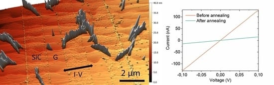
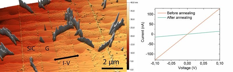
In order to assess the quality of graphene as a contact for polymer nanofibers, we chose polyaniline (PANI) as the conductive channel medium. PANI nanofibers have a unique acid/base doping/dedoping chemistry that is reversibly switchable from the doped state to the dedoped state by exposure to hydrochloric acid and ammonia [44,45,46]. Together with the enhanced surface to volume ratio in nanofiber morphology, PANI nanofibers are also promising for gas sensing applications [1,47,48]. Besides, the carbonization of polymers by pyrolysis [49,50,51,52,53,54,55,56,57,58] shows potential for applications such as a fuel cell [53] and catalyst [56,57], and PANI produces nitrogen containing conducting carbons after pyrolysis [52,53,54,55,56,57,58]. On the as-fabricated G/SiC electrode, a suspension of solution containing PANI nanofibers were dispersed (see Method) and we observed that fibers readily form an Ohmic contact to graphene electrodes. Furthermore, the thermal stability of epitaxial graphene electrodes allows thermal processes at elevated temperatures to be carried out. Indeed, we annealed the device up to T = 800 °C and found that the contact between graphene and fibers remain Ohmic. We performed the thermal annealing cycle under continuous argon flow to prevent oxidation of organic species. This method allowed us to investigate not only the thermal stability of the PANI nanofiber-G/SiC devices but also to explore the electron transport properties of carbonized polymer nanofibers in general [59]. Figure 3a,b show the AFM topography of PANI nanofibers contacted on G/SiC electrodes before and after T = 800 °C annealing, respectively. Upon high temperature annealing, the G/SiC electrode remains intact and most of the PANI nanofibers were preserved as shown in Figure 3b. Comparison of Figure 3a,b at the same area before and after annealing, shows that the overall shape of the nanofibers is retained; however, both the width and the height of PANI nanofibers are significantly reduced to about 50% after annealing (Figure 3c). This is consistent with previous reports that PANI undergoes dehydrogenation and cross-linking of adjacent chains upon high temperature pyrolysis, and that the weight of polyacetylene (PA) films/fibers [49,50,51] and PANI films/tubes [52,53,54,55,56,57,58] is reduced after pyrolysis while retaining the fibril morphology. I-V characteristics of the PANI nanofibers on G/SiC electrodes before annealing show that the adjacent G/SiC leads are electrically connected due to the PANI nanofibers contacting the two adjacent G/SiC electrodes. The device shows linear and symmetric I-V characteristics of PANI nanofibers on G/SiC before and after annealing, with the resistance increased about 10 times upon annealing. The symmetric and linear I-V is consistent with previous reports regarding annealed PANI nanofibers at 800 °C [59].
We verified the integrity of the devices, including the graphene contacts, after the thermal annealing step by Raman spectroscopy and found that PANI fibers undergo carbonization but graphene remains essentially intact. Figure 4 shows the Raman spectroscopy (λ = 638 nm) measured on bundles of PANI nanofibers (Figure 4a) and of G/SiC (Figure 4b) before and after annealing. We found substantial changes in the PANI nanofiber after annealing. In the pristine form, the Raman spectra of PANI nanofibers show complex peaks that indicates PANI nanofibers. Raman spectroscopy on the annealed PANI nanofiber bundles shows that the PANI nanofibers become amorphous carbon nanofibers as confirmed by the broad D (1353 cm−1) and G bands (1590 cm−1) of graphite (Figure 4b) [49,50,51,52,53,54,55,56,57,58,59]. In contrast, the G/SiC remained intact after annealing as shown in Figure 4b. Figure 4b displays the Raman spectra of the pristine, annealed G/SiC, and the etched SiC region as a reference. The Raman spectra on G/SiC includes contributions both from the bulk SiC substrate and the so-called buffer layer. Therefore, correcting the Raman spectra of G/SiC by subtracting the spectrum of SiC substrate may introduce artifacts due to the contribution of the substrate [60]. The presence of G and 2D peaks before and after annealing means that the G/SiC remains intact after annealing [60,61]. The thermal stability of graphene is comparable to that of oxides such as Sr2RuO4 (stable at 900 °C) [62] and olivine (stable at 500 °C) electrodes [63].
2.3. Comparison of Graphene with Gold as a Contact for PANI Nanofibers
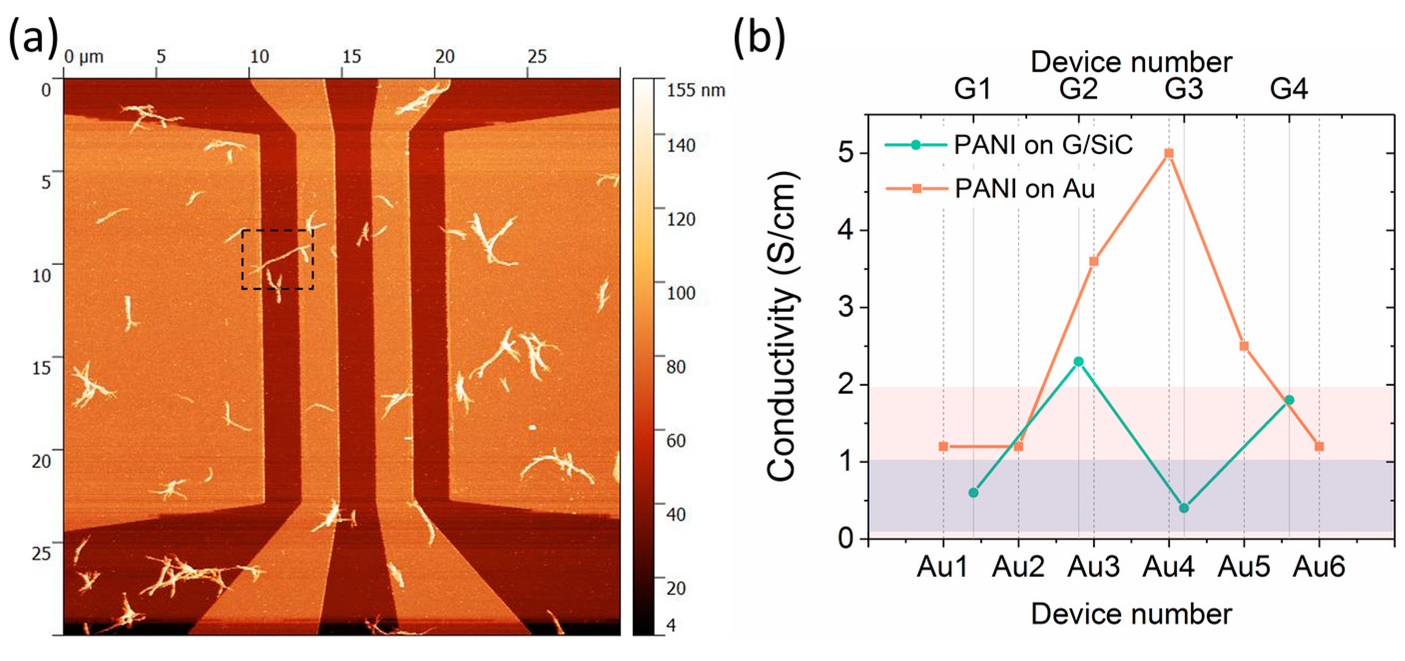
We benchmarked graphene as a contact for polymer nanofibers against gold, which is the standard contact metal for these materials. Figure 5a shows the AFM topography of a Ti/Au electrode deposited on a Si/SiO2 (300 nm) substrate and a PANI nanofiber contacted on Au electrodes. The conductivity and height of PANI nanofibers measured on both G/SiC and Au electrodes of this study range from 0.5–5 S/cm and 50–110 nm, respectively. Figure 5b compares the conductivity of PANI nanofibers on graphene electrodes (G1–G4) (see Methods and Figures S5–S7) to that on Au electrodes (Au1–Au6) (see Methods and Figures S1–S4). The conductivity of PANI nanofibers on G/SiC electrodes (0.5–2.3 S/cm) was slightly lower than that on Au (1.2–5 S/cm); however, this is comparable with the conductivity of PANI nanofibers measured on Au electrodes reported in the literature [64].
3. Materials and Methods
3.1. Growth of Epitaxial Graphene on SiC
The graphene was purchased from Graphensic AB. The crystallographic orientation of the 4H-SiC substrate is (0001) which provides large terraces and minimizes bilayer inclusions. The graphene fabrication process includes standard two-step cleaning procedure including HF solution dipping prior to loading into the growth reactor. The latter consists of a vertical radio frequency (RF) heated graphite crucible placed in a quartz tube with a thermal insulation between their walls. Upon reaching base vacuum in the range of 10−6 mbar, heating is performed until 2000 °C and this temperature is held for 5 min. After that the RF generator is switched off and the graphene wafer is cooled down to room temperature. The wafer is subjected to microscopy examination to check the graphene morphology and after that, to further processing steps.
3.2. Fabrication of Graphene and Au Electrodes
3.2.1. Fabrication of Graphene Electrodes
Graphene electrodes in Figure 2 and of devices G1–G4 were fabricated on the as-grown graphene on the Si face of the 4H-SiC surface. For the first step, Al (20 nm) was deposited to avoid resist residue and the standard electron beam lithography (EBL) using e-beam resist ARP-6200 (Allresist, Strausberg, Germany) was performed on top of Al. After developing the e-beam resist, a MF-319 photodeveloper (Dow Europe, Horgen, Switzerland) was used for the wet etch of Al underneath and the exposed graphene was dry-etched using oxygen plasma (Figure 1b). After dissolving the remaining resist in organic solvent mr-REM-400 (Micro resist Tech., Berlin, Germany) (Figure 1c), the second EBL was employed for global Ti/Au (5/100 nm) contacts to the G/SiC leads for wire bonding. Before depositing Ti/Au for the global contact, Al was wet-etched using MF-319 photodeveloper (Figure 1e) to ensure contact between graphene and Ti/Au.
3.2.2. Fabrication of Gold Electrodes
Au electrodes in devices Au1–Au6 were fabricated by standard EBL using a poly(methylmethacrylate) (PMMA) (MicroChem, Westborough, MA, USA) double layer mask on Si/SiO2 (300 nm) substrates. We used the same electrode design that was used for graphene electrodes and Ti/Au (5/50 nm) was evaporated on the patterned PMMA and lifted off in organic solvent acetone. The thickness of Ti/Au (5/50 nm) was chosen to be comparable with the height of typical PANI nanofibers.
3.3. Synthesis of Polyaniline Nanofibers and Contacting to Graphene and Au Electrodes
PANI nanofibers were synthesized using a known synthesis protocol [44,45,46]. 0.08 mmol of aniline (Sigma-Aldrich, St. Louis, MO, USA) was dissolved in 10 mL of 1 M HCl and a catalytic amount of p-phenylenediamine (5 mg) (Sigma-Aldrich, St. Louis, MO, USA) in a minimal amount of methanol was added into the aniline solution. 0.2 mmol of ammonium peroxidisulfate (Sigma-Aldrich, St. Louis, MO, USA) was dissolved in 10 mL of 1 M HCl and the two prepared solutions were rapidly mixed for 10 s and left for one day. A droplet of the suspension of the PANI nanofibers doped by hydrochloric acid was deposited on both the G/SiC and Au electrodes and blow-dried. Then we inspected these under optical and atomic force microscope and selected those devices in which single fibers are contacted. The probability of finding such devices is low, and we presented 6 devices in total (3 graphene contacts and 3 gold contacts) and also presented 4 devices corresponding to three or four polymer nanofibers (1 graphene contact and 3 gold contacts). The AFM and I-V curves of the nanofibers on graphene (G1–G4) and on Au (Au1–Au6) are described in detail in the Supplementary Materials.
3.4. Electrical Characterization, Raman Spectroscopy and Carbonization
Electrical characterization of G/SiC electrodes, PANI nanofibers on G/SiC and Au electrodes, and the annealed devices was carried out using the Semiconductor Characterization System (SCS) parameter analyzer (Keithley Instruments, Solon, OH, USA) at room temperature under ambient conditions in both two-terminal and four-terminal configurations. Raman spectroscopy measurement was performed under ambient conditions using a Raman spectrometer equipped with a spot size ~1 μm (λ = 638 nm) (Horiba Scientific, Longjumeau, France). The signal acquisition time was one minute and averaged 5 times due to the relatively small signal of the graphene compared with the signal from the SiC substrate. The annealing took place in a tube furnace at 800 °C for one hour under argon flow with automated ramping rate of 1 °C/min in both heating and cooling steps.
4. Conclusions
In conclusion, we used epitaxial graphene on SiC as Ohmic contacts to polymer nanofibers. We showed that G/SiC-PANI devices exhibit a conductivity comparable to that of PANI nanofibers on Au electrodes. Thermal annealing of the G/SiC-PANI nanofiber device showed that the device is intact after 800 °C annealing and that the PANI nanofibers become amorphous carbons with reduced height and width, making epitaxial graphene contacts promising for applications that require operation at high temperature. While the thermal stability of G/SiC is comparable to that of other materials, graphene offers additional properties such as chemical stability and atomic flatness that make it an attractive platform as a substrate and contact material for future all-carbon devices.
Supplementary Materials
The following are available online at www.mdpi.com/2073-4352/7/12/378/s1, Figure S1: Device Au1–Au3 (a) Atomic force microscope topography of PANI contacted between Au contacts 1-2, 2-3, and 3-4 (Au1, Au2, Au3, respectively); (b) Current-Voltage characteristics of PANI nanofibers contacted between contact 1-2 (Au1), 2-3 (Au2), 3-4 (Au3), and four-probe measurement; Figure S2: Device Au4 (a) Atomic force microscope topography of PANI contacted between Au contacts 1-2 (Au4); (b) Current-Voltage characteristics of the PANI nanofiber contacted between contacts 1-2 (Au4); Figure S3: Device Au5 (a) Atomic force microscope topography of PANI contacted between Au contacts 1-2 (Au5); (b) Current-Voltage characteristics of the PANI nanofiber contacted between contacts 1-2 (Au5); Figure S4: Device Au6 (a) Atomic force microscope topography of PANI contacted between Au contacts 1-2 (Au6); (b) Current-Voltage characteristics of the PANI nanofibers contacted between contacts 1-2 (Au1); Figure S5: Device G1 (a) AFM phase of PANI contacted between G/SiC contacts 1-2 (G1). We checked that the electrodes (1) and (2) were electrically insulating before nanofiber deposition. ((2) and (3) were electrically shorted due to incomplete graphene etching as shown in the AFM phase image); (b) Current-Voltage characteristics of the PANI nanofiber contacted between contacts 1-2 (G1) before and after T = 800 °C annealing. In this device, the electrical resistance decreased after annealing; Figure S6: G2 (a) AFM phase of PANI contacted G/SiC contact 1-2 (G2). We checked that the electrodes (1) and (2) were electrically insulating before nanofiber deposition. (b) Current-Voltage characteristics of the PANI nanofiber contacted between contact 1-2 (G2) before T = 800 °C annealing. After annealing the nanofiber was cut and not conductive; Figure S7: G3 and G4 AFM topography (a) and phase (b) of PANI contacted G/SiC on contact 1-2 (G3), 2-3 (G4), and 3-4. The device shown in Figure 3 is G4 and among the three PANI nanofibers in G4, the nanofiber in Figure 3 is in the middle of the electrode. We checked that the electrodes (1), (2), (3), and (4) were electrically insulating each other before nanofiber deposition. (c) and (d) are the AFM topography and phase after T = 800 °C annealing, respectively; (e) Current-Voltage characteristics of the PANI nanofiber contacted between contacts 1-2 (G3), 2-3 (G4), and 3-4 before T = 800 °C annealing. (f) Current-Voltage characteristics of the PANI nanofiber contacted between contacts 1-2 (G3), 2-3 (G4), and 3-4 after T = 800 °C annealing. Scale bars in (a)–(d) are 10 um; Table S1: Summary of PANI-Au devices (Au1–Au6) in height, source-drain distance, and conductivity; Table S2: Summary of PANI-G/SiC devices (G1–G6) in height, source-drain distance and conductivity.
Acknowledgments
This work was jointly supported by the Swedish-Korean Basic Research Cooperative Program of the National Research Foundation (NRF) NRF-2017R1A2A1A18070721, the Swedish Foundation for Strategic Research (SSF) IS14-0053, GMT14-0077, RMA15-0024, Swedish Research Council, Knut and Alice Wallenberg Foundation, and Chalmers Area of Advance NANO. Partial support was provided by the GRDC (2015K1A4A3047345), the FPRD of BK21 from the NRF through the Ministry of Science, ICT Future Planning (MSIP), Korea.
Author Contributions
Sergey Kubatkin, Yung Woo Park, Samuel Lara-Avila and Kyung Ho Kim conceived and designed the experiments; Kyung Ho Kim and Hans He performed the experiments and Kyung Ho Kim analyzed the data; Hojin Kang contributed to polyaniline synthesis; Rositsa Yakimova developed the process for G/SiC growth; Kyung Ho Kim and Samuel Lara-Avila wrote the paper. All authors reviewed the manuscript.
Conflicts of Interest
The authors declare no conflict of interest. The funding sponsors had no role in the design of the study; in the collection, analyses, or interpretation of data; in the writing of the manuscript, and in the decision to publish the results.
References
- Chen, D.; Lei, S.; Chen, Y. A single polyaniline nanofiber field effect transistor and its gas sensing mechanisms. Sensors 2011, 11, 6509–6516. [Google Scholar] [CrossRef] [PubMed]
- Baker, C.O.; Shedd, B.; Innis, P.C.; Whitten, P.G.; Spinks, G.M.; Wallace, G.G.; Kaner, R.B. Monolithic actuators from flash-welded polyaniline nanofibers. Adv. Mater. 2008, 20, 155–158. [Google Scholar] [CrossRef]
- Chen, X.; Wong, C.K.Y.; Yuan, C.A.; Zhang, G. Nanowire-based gas sensors. Sens. Actuators B Chem. 2013, 177, 178–195. [Google Scholar] [CrossRef]
- Yu, H.; Li, B. Wavelength-converted wave-guiding in dye-doped polymer nanofibers. Sci. Rep. 2013, 3, 1674. [Google Scholar] [CrossRef] [PubMed]
- Park, J.U.; Nam, S.; Lee, M.S.; Lieber, C.M. Synthesis of monolithic graphene–graphite integrated electronics. Nat. Mater. 2011, 11, 120–125. [Google Scholar] [CrossRef] [PubMed] [Green Version]
- Liu, W.; Wei, J.; Sun, X.; Yu, H. A Study on graphene—metal contact. Crystals 2013, 3, 257–274. [Google Scholar] [CrossRef]
- Lin, Y.M.; Valdes-Garcia, A.; Han, S.J.; Farmer, D.B.; Meric, I.; Sun, Y.N.; Wu, Y.Q.; Dimitrakopoulos, C.; Grill, A.; Avouris, P.; et al. Wafer-scale graphene integrated circuit. Science 2011, 332, 1294–1298. [Google Scholar] [CrossRef] [PubMed]
- Neto, A.H.C.; Guinea, F.; Peres, N.M.R.; Novoselov, K.S.; Geim, A.K. The electronic properties of graphene. Rev. Mod. Phys. 2009, 81, 109–162. [Google Scholar] [CrossRef] [Green Version]
- Banszerus, L.; Schmitz, M.; Engels, S.; Dauber, J.; Oellers, M.; Haupt, F.; Watanabe, K.; Taniguchi, T.; Beschoten, B.; Stampfer, C. Ultrahigh-mobility graphene devices from chemical vapor deposition on reusable copper. Sci. Adv. 2015, 1, e1500222. [Google Scholar] [CrossRef] [PubMed]
- Yager, T.; Webb, M.J.; Grennberg, H.; Yakimova, R.; Lara-Avila, S.; Kubatkin, S. High mobility epitaxial graphene devices via aqueous-ozone processing. Appl. Phys. Lett. 2015, 106, 063503. [Google Scholar] [CrossRef]
- Boyd, D.A.; Lin, W.H.; Hsu, C.C.; Teague, M.L.; Chen, C.C.; Lo, Y.Y.; Chan, W.Y.; Su, W.B.; Cheng, T.C.; Chang, C.S.; et al. Single-step deposition of high-mobility graphene at reduced temperatures. Nat. Commun. 2015, 6, 6620. [Google Scholar] [CrossRef] [PubMed]
- Balandin, A.A.; Ghosh, S.; Bao, W.; Calizo, I.; Teweldebrhan, D.; Miao, F.; Lau, C.N. Superior thermal conductivity of single-layer graphene. Nano Lett. 2008, 8, 902–907. [Google Scholar] [CrossRef] [PubMed]
- Nair, R.R.; Blake, P.; Grigorenko, A.N.; Novoselov, K.S.; Booth, T.J.; Stauber, T.; Peres, N.M.R.; Geim, A.K. Fine structure constant defines visual transparency of graphene. Science 2008, 320, 1308. [Google Scholar] [CrossRef] [PubMed]
- Bonaccorso, F.; Sun, Z.; Hasan, T.; Ferrari, A.C. Graphene photonics and optoelectronics. Nat. Photonics 2010, 4, 611–622. [Google Scholar] [CrossRef]
- Mansour, A.E.; Said, M.M.; Dey, S.; Hu, H.; Zhang, S.; Munir, R.; Zhang, Y.; Moudgil, K.; Barlow, S.; Marder, S.R.; et al. Facile doping and work-function modification of few-layer graphene using molecular oxidants and reductants. Adv. Funct. Mater. 2017, 27, 1602004. [Google Scholar] [CrossRef]
- Hong, S.K.; Song, S.M.; Sul, O.; Cho, B.J. Reduction of metal-graphene contact resistance by direct growth of graphene over metal. Carbon Lett. 2013, 14, 171–174. [Google Scholar] [CrossRef]
- Lee, S.; Jo, G.; Kang, S.J.; Park, W.; Kahng, Y.H.; Kim, D.Y.; Lee, B.H.; Lee, T. Characterization on improved effective mobility of pentacene organic field-effect transistors using graphene electrodes. Jpn. J. Appl. Phys. 2012, 51, 02BK09. [Google Scholar] [CrossRef]
- Liu, W.; Jackson, B.L.; Zhu, J.; Miao, C.; Park, Y.; Sun, K.; Woo, J.; Xie, Y. Large scale pattern graphene electrode for high performance in transparent organic single crystal field-effect transistors. ACS Nano 2010, 4, 3927–3932. [Google Scholar] [CrossRef] [PubMed]
- Cao, Y.; Liu, S.; Shen, Q.; Yan, K.; Li, P.; Xu, J.; Yu, D.; Steigerwald, M.L.; Nuckolls, C.; Liu, Z.; et al. High-performance photoresponsive organic nanotransistors with single-layer graphenes as two-dimensional electrodes. Adv. Funct. Mater. 2009, 19, 2743–2748. [Google Scholar] [CrossRef]
- Park, J.K.; Song, S.M.; Mun, J.H.; Cho, B.J. Graphene gate electrode for MOS structure-based electronic devices. Nano Lett. 2011, 11, 5383–5386. [Google Scholar] [CrossRef] [PubMed]
- Di, C.A.; Wei, D.; Yu, G.; Liu, Y.; Guo, Y.; Zhu, D. Patterned graphene as source/drain electrodes for bottom-contact organic field-effect transistors. Adv. Mater. 2008, 20, 3289–3293. [Google Scholar] [CrossRef]
- Pang, S.; Tsao, H.N.; Feng, X.; Mullen, K. Patterned graphene electrodes from solution-processed graphite oxide films for organic field-effect transistors. Adv. Mater. 2009, 21, 3488–3491. [Google Scholar] [CrossRef]
- Henrichsen, H.H.; Bøggild, P. Graphene electrodes for n-type organic field-effect transistors. Microelectron. Eng. 2010, 87, 1120–1122. [Google Scholar] [CrossRef]
- Wang, X.; Zhi, L.; Müllen, K. Transparent, conductive graphene electrodes for dye-sensitized solar cells. Nano Lett. 2008, 8, 323–327. [Google Scholar] [CrossRef] [PubMed]
- Jo, G.; Choe, M.; Cho, C.Y.; Kim, J.H.; Park, W.; Lee, S.; Hong, W.K.; Kim, T.W.; Park, S.J.; Hong, B.H.; et al. Large-scale patterned multi-layer graphene films as transparent conducting electrodes for GaN light-emitting diodes. Nanotechnol. 2010, 21, 175201. [Google Scholar] [CrossRef] [PubMed]
- Qian, Z.; Hui, Y.; Liu, F.; Kang, S.; Kar, S.; Rinaldi, M. Graphene–aluminum nitride NEMS resonant infrared detector. Microsyst. Nanoeng. 2016, 2, 16026. [Google Scholar] [CrossRef]
- Kuzum, D.; Takano, H.; Shim, E.; Reed, J.C.; Juul, H.; Richardson, A.G.; de Vries, J.; Bink, H.; Dichter, M.A.; Lucas, T.H.; et al. Transparent and flexible low noise graphene electrodes for simultaneous electrophysiology and neuroimaging. Nat. Commun. 2014, 5, 5259. [Google Scholar] [CrossRef] [PubMed]
- Park, D.W.; Brodnick, S.K.; Ness, J.P.; Atry, F.; Krugner-Higby, L.; Sandberg, A.; Mikael, S.; Richner, T.J.; Novello, J.; Kim, H.; et al. Fabrication and utility of a transparent graphene neural electrode array for electrophysiology, in vivo imaging, and optogenetics. Nat. Protoc. 2016, 11, 2201–2222. [Google Scholar] [CrossRef] [PubMed]
- Vashist, S.K.; Luong, J.H.T. Recent advances in electrochemical biosensing schemes using graphene and graphene-based nanocomposites. Carbon 2015, 84, 519–550. [Google Scholar] [CrossRef]
- Vashist, S.K.; Luppa, P.B.; Yeo, L.Y.; Ozcan, A.; Luong, J.H.T. Emerging Technologies for Next-Generation Point-of-Care Testing. Trends Biotechnol. 2015, 33, 692–705. [Google Scholar] [CrossRef] [PubMed]
- Zhu, Y.; Sun, Z.; Yan, Z.; Jin, Z.; Tour, J.M. Rational design of hybrid graphene films for high-performance transparent electrodes. ACS Nano 2011, 5, 6472–6479. [Google Scholar] [CrossRef] [PubMed]
- Yager, T.; Lartsev, A.; Yakimova, R.; Lara-Avila, S.; Kubatkin, S. Wafer-scale homogeneity of transport properties in epitaxial graphene on SiC. Carbon 2015, 87, 409–414. [Google Scholar] [CrossRef]
- Yazdi, G.; Iakimov, T.; Yakimova, R. Epitaxial graphene on SiC: A review of growth and characterization. Crystals 2016, 6, 53. [Google Scholar] [CrossRef]
- Shih, F.Y.; Chen, S.Y.; Liu, C.H.; Ho, P.H.; Wu, T.S.; Chen, C.W.; Chen, Y.F.; Wang, W.H. Residue-free fabrication of high-performance graphene devices by patterned PMMA stencil mask. AIP Adv. 2014, 4, 67129. [Google Scholar] [CrossRef]
- Kybert, N.J.; Han, G.H.; Lerner, M.B.; Dattoli, E.N.; Esfandiar, A.; Charlie Johnson, A.T. Scalable arrays of chemical vapor sensors based on DNA-decorated graphene. Nano Res. 2014, 7, 95–103. [Google Scholar] [CrossRef]
- Yong, K.; Ashraf, A.; Kang, P.; Nam, S. Rapid stencil mask fabrication enabled one-step polymer-free graphene patterning and direct transfer for flexible graphene devices. Sci. Rep. 2016, 6, 24890. [Google Scholar] [CrossRef] [PubMed]
- Hsu, A.; Wang, H.; Kim, K.K.; Kong, J.; Palacios, T. Impact of graphene interface quality on contact resistance and RF device performance. IEEE. Electron. Device Lett. 2011, 32, 1008–1010. [Google Scholar] [CrossRef]
- Xie, W.; Weng, L.T.; Ng, K.M.; Chan, C.K.; Chan, C.M. Clean graphene surface through high temperature annealing. Carbon 2015, 94, 740–748. [Google Scholar] [CrossRef]
- Yager, T.; Lartsev, A.; Mahashabde, S.; Charpentier, S.; Davidovikj, D.; Danilov, A.; Yakimova, R.; Panchal, V.; Kazakova, O.; Tzalenchuk, A.; et al. Express optical analysis of epitaxial graphene on SiC: Impact of morphology on quantum transport. Nano Lett. 2013, 13, 4217–4223. [Google Scholar] [CrossRef] [PubMed]
- Kopylov, S.; Tzalenchuk, A.; Kubatkin, S.; Fal’Ko, V.I. Charge transfer between epitaxial graphene and silicon carbide. Appl. Phys. Lett. 2010, 97, 112109. [Google Scholar] [CrossRef]
- Janssen, T.J.B.M.; Tzalenchuk, A.; Yakimova, R.; Kubatkin, S.; Lara-Avila, S.; Kopylov, S.V.; Fal’Ko, V.I. Anomalously strong pinning of the filling factor ν = 2 in epitaxial graphene. Phys. Rev. B. 2011, 83, 233402. [Google Scholar] [CrossRef]
- Leong, W.S.; Nai, C.T.; Thong, J.T.L. What does annealing do to metal-graphene contacts? Nano Lett. 2014, 14, 3840–3847. [Google Scholar] [CrossRef] [PubMed]
- Yager, T.; Lartsev, A.; Cedergren, K.; Yakimova, R.; Panchal, V.; Kazakova, O.; Tzalenchuk, A.; Kim, K.H.; Park, Y.W.; Lara-Avila, S.; et al. Low contact resistance in epitaxial graphene devices for quantum metrology. AIP Adv. 2015, 5, 087134. [Google Scholar] [CrossRef]
- Tran, H.D.; Wang, Y.; D’Arcy, J.M.; Kaner, R.B. Toward an understanding of the formation of conducting polymer nanofibers. ACS Nano 2008, 2, 1841–1848. [Google Scholar] [CrossRef] [PubMed]
- Huang, J.; Kaner, R.B. The intrinsic nanofibrillar morphology of polyaniline. Chem. Commun. 2006, 0, 367–376. [Google Scholar] [CrossRef] [PubMed]
- Tran, H.D.; Norris, I.; D’Arcy, J.M.; Tsang, H.; Wang, Y.; Mattes, B.R.; Kaner, R.B. Substituted polyaniline nanofibers produced via rapid initiated polymerization. Macromolecular 2008, 41, 7405–7410. [Google Scholar] [CrossRef]
- Wu, Z.; Chen, X.; Zhu, S.; Zhou, Z.; Yao, Y.; Quan, W.; Liu, B. Enhanced sensitivity of ammonia sensor using graphene/polyaniline nanocomposite. Sens. Actuators B Chem. 2013, 178, 485–493. [Google Scholar] [CrossRef]
- Crowley, K.; Smyth, M.; Killard, A.; Morrin, A. Printing polyaniline for sensor applications. Chem. Pap. 2013, 67, 771–780. [Google Scholar] [CrossRef]
- Goto, A.; Kyotani, M.; Tsugawa, K.; Piao, G.; Akagi, K.; Yamaguchi, C.; Matsui, H.; Koga, Y. Nanostructures of pyrolytic carbon from a polyacetylene thin film. Carbon 2003, 41, 131–138. [Google Scholar] [CrossRef]
- Kyotani, M.; Matsushita, S.; Nagai, T.; Matsui, Y.; Shimomura, M.; Kaito, A.; Akagi, K. Helical carbon and graphitic films prepared from iodine-doped helical polyacetylene film using morphology-retaining carbonization. J. Am. Chem. Soc. 2008, 130, 10880–10881. [Google Scholar] [CrossRef] [PubMed]
- Matsushita, S.; Akagi, K. Macroscopically aligned graphite films prepared from iodine-doped stretchable polyacetylene films using morphology-retaining carbonization. J. Am. Chem. Soc. 2015, 137, 9077–9087. [Google Scholar] [CrossRef] [PubMed]
- Bober, P.; Trchová, M.; Morávková, Z.; Kovářová, J.; Vulić, I.; Gavrilov, N.; Pašti, I.A.; Stejskal, J. Phosphorus and nitrogen-containing carbons obtained by the carbonization of conducting polyaniline complex with phosphites. Electrochem. Acta 2017, 246, 443–450. [Google Scholar] [CrossRef]
- Maiyalagan, T.; Viswanathan, B.; Varadaraju, U.V. Nitrogen containing carbon nanotubes as supports for Pt-Alternate anodes for fuel cell applications. Electrochem. Commun. 2005, 7, 905–912. [Google Scholar] [CrossRef]
- Rozlívková, Z.; Trchová, M.; Exnerová, M.; Stejskal, J. The carbonization of granular polyaniline to produce nitrogen-containing carbon. Synth. Met. 2011, 161, 1122–1129. [Google Scholar] [CrossRef]
- Trchová, M.; Konyushenko, E.N.; Stejskal, J.; Kovářová, J.; Ćirić-Marjanović, G. The conversion of polyaniline nanotubes to nitrogen-containing carbon nanotubes and their comparison with multi-walled carbon nanotubes. Polym. Degrad. Stab. 2009, 94, 929–938. [Google Scholar] [CrossRef]
- Quílez-Bermejo, J.; González-Gaitan, C.; Morallón, E.; Cazorla-Amorós, D. Effect of carbonization conditions of polyaniline on its catalytic activity towards ORR. Some insights about the nature of the active sites. Carbon 2017, 119, 62–71. [Google Scholar] [CrossRef]
- Shen, W.; Fan, W. Nitrogen-containing porous carbons: synthesis and application. J. Mater. Chem. A 2013, 1, 999–1013. [Google Scholar] [CrossRef]
- Mentus, S.; Ćirić-Marjanović, G.; Trchová, M.; Stejskal, J. Conducting carbonized polyaniline nanotubes. Nanotechnology 2009, 20, 245601. [Google Scholar] [CrossRef] [PubMed]
- Kim, K.H.; Lara-Avila, S.; Kang, H.; He, H.; Eklӧf, J.; Hong, S.J.; Park, M.; Moth-Poulsen, K.; Matsushita, S.; Akagi, K.; et al. Apparent power law scaling of variable range hopping conduction in carbonized polymer nanofibers. Sci. Rep. 2016, 6, 37783. [Google Scholar] [CrossRef] [PubMed]
- Fromm, F.; Oliveira, M.H.; Molina-Sánchez, A.; Hundhausen, M.; Lopes, J.M.J.; Riechert, H.; Wirtz, L.; Seyller, T. Contribution of the buffer layer to the Raman spectrum of epitaxial graphene on SiC(0001). New J. Phys. 2013, 15, 043031. [Google Scholar] [CrossRef]
- Lee, D.S.; Riedl, C.; Krau, B.; Klitzing, K.V.; Starke, U.; Smet, J.H.; Festkörperforschung, M.; Stuttgart, D. Raman spectra of epitaxial graphene on SiC and of epitaxial graphene transferred to SiO2. Nano Lett. 2008, 8, 4320–4325. [Google Scholar] [CrossRef] [PubMed]
- Takahashi, R.; Lippmaa, M. Thermally Stable Sr2RuO4 Electrode for Oxide Heterostructures. ACS Appl. Mater. Interfaces 2017, 9, 21314–21321. [Google Scholar] [CrossRef] [PubMed]
- Park, K.Y.; Kim, H.; Lee, S.; Kim, J.; Hong, J.; Lim, H.D.; Park, I.; Kang, K. Thermal structural stability of multi-component olivine electrode for lithium ion batteries. CrystEngComm 2016, 18, 7463–7470. [Google Scholar] [CrossRef]
- Choi, A.J. Magneto Resistance of One-Dimensional Polymer Nanofibers. Ph.D. Thesis, Seoul National University, Seoul, Korea, February 2012. [Google Scholar]
Figure 1.
The schematic illustration of the fabrication process of the G/SiC electrode: (a) As-grown epitaxial graphene on SiC (G/SiC); (b) An aluminum protection layer was first deposited on G/SiC, and this was followed by electron beam lithography (EBL) and successive graphene etching in oxygen plasma; (c) Resist is removed with organic solvents; (d) A second EBL step for defining global Ti/Au contacts (e) Al removal by wet etching; (f) Deposition of Ti/Au global contacts on G/SiC electrodes and lift-off in organic solvents.

Figure 2.
Thermal stability of graphene electrodes. (a) The optical microscope image of the G/SiC electrode with width (length) 1 μm (10 μm). Scale bar: 10 μm; (b) The linear current-voltage (I-V) characteristics of the G/SiC lead marked by arrows in (a) before and after annealing at T = 800 °C. The adjacent leads are insulated before and after annealing and the resistance of the G/SiC lead decreased after the T = 800 °C annealing.

Figure 3.
Characterization of graphene-nanofiber devices before and after the thermal annealing step. (a) Atomic force microscopy (AFM) topography image of G/SiC electrodes contacting polyaniline (PANI) nanofibers, where graphene leads are indicated by G.; (b) AFM topography image of (a) after thermal annealing at T = 800 °C. The graphene leads remain intact and morphology of PANI nanofibers are preserved. Scale bar: 2 μm; (c); The reduction in size of PANI nanofibers after annealing is compared in the AFM height profile of the region indicated by blue lines in (a,b). Both the width (320 nm to 190 nm) and height (65 nm to 28 nm) are reduced after annealing; (d) I-V characteristics of the adjacent graphene electrodes before and after annealing. Between the two electrodes in which I-V was measured, three PANI nanofibers are contacted in total (Device G4, see Figure S7). After annealing, the resistance typically increases to 10 times.
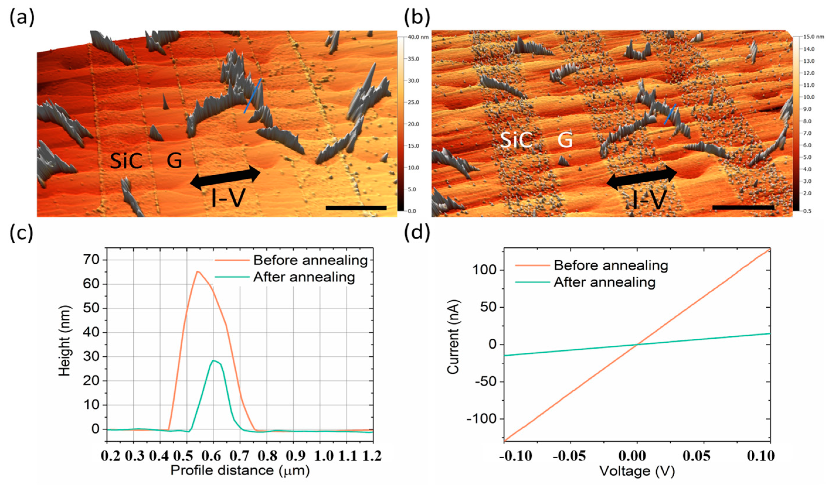
Figure 4.
Raman spectroscopy before and after annealing (a) Raman spectroscopy on a bundle of PANI nanofibers before and after 800 °C annealing. After annealing, the complex peaks in PANI nanofibers turned to two broad peaks marked by D and G bands. The intensity of PANI is normalized with respect to the maximum value of D band in annealed PANI nanofibers; (b) Raman spectroscopy of the pristine graphene, annealed graphene and SiC. Dotted boxes indicate the vicinity of D, G, and 2D peaks. The intensity is normalized by the highest peak of Raman spectra measured on the SiC substrate.
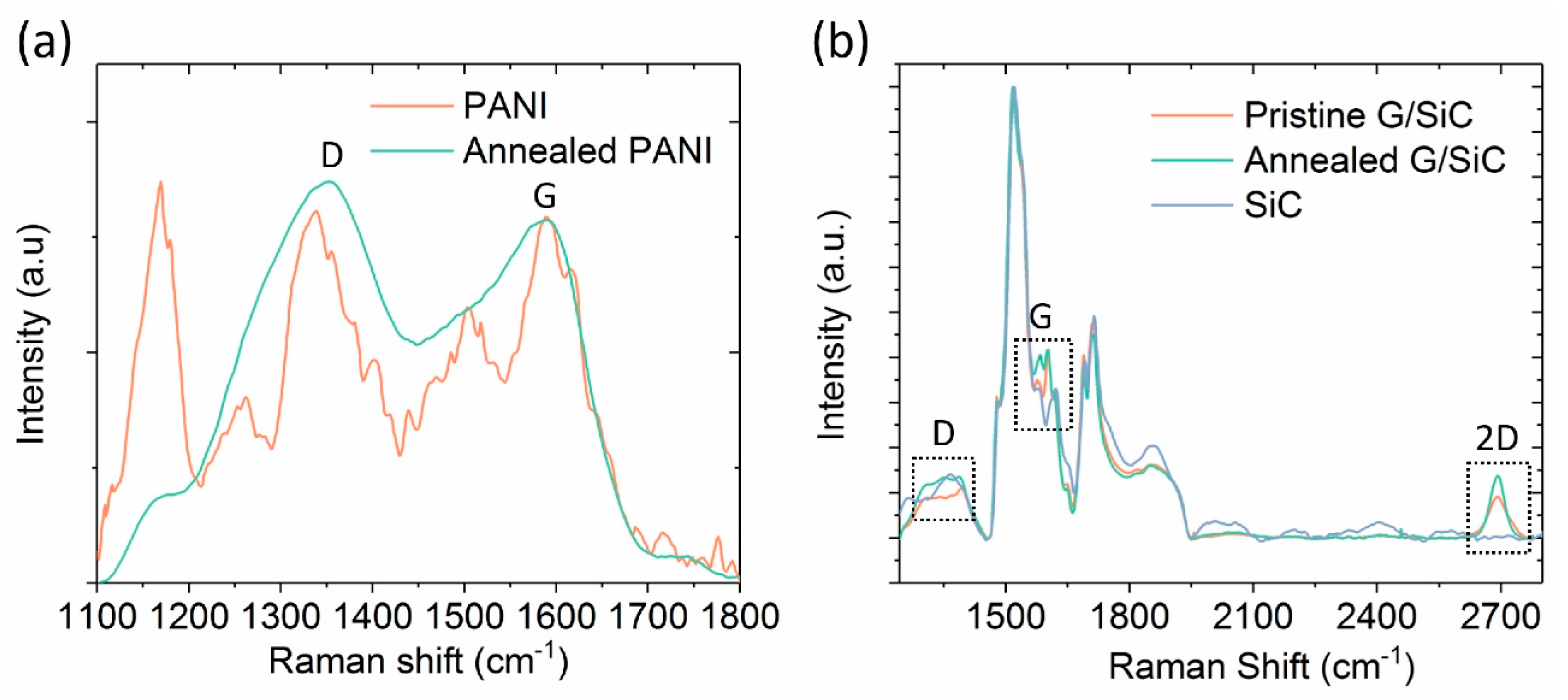
Figure 5.
Comparison of graphene and gold as contact for PANI nanofibers. (a) AFM topography of PANI nanofibers contacted on Au electrodes (Au4, Figure S2). The contact of a PANI nanofiber contacted by Au electrodes is indicated by a dotted box; (b) Conductivity of PANI nanofibers measured on both Au (Au1–Au6, Figures S1–S4) and graphene electrodes (G1–G4, Figures S5–S7). The blue (red) shaded region is the conductivity of PANI nanofibers (annealed PANI nanofibers at 800 °C) measured on Au electrodes in Ref [64] (Ti/Au bottom contact electrode in Ref. [59]).

© 2017 by the authors. Licensee MDPI, Basel, Switzerland. This article is an open access article distributed under the terms and conditions of the Creative Commons Attribution (CC BY) license (http://creativecommons.org/licenses/by/4.0/).
Share and Cite
MDPI and ACS Style
Kim, K.H.; Lara-Avila, S.; He, H.; Kang, H.; Park, Y.W.; Yakimova, R.; Kubatkin, S. Thermal Stability of Epitaxial Graphene Electrodes for Conductive Polymer Nanofiber Devices. Crystals 2017, 7, 378. https://doi.org/10.3390/cryst7120378
AMA Style
Kim KH, Lara-Avila S, He H, Kang H, Park YW, Yakimova R, Kubatkin S. Thermal Stability of Epitaxial Graphene Electrodes for Conductive Polymer Nanofiber Devices. Crystals. 2017; 7(12):378. https://doi.org/10.3390/cryst7120378
Chicago/Turabian StyleKim, Kyung Ho, Samuel Lara-Avila, Hans He, Hojin Kang, Yung Woo Park, Rositsa Yakimova, and Sergey Kubatkin. 2017. "Thermal Stability of Epitaxial Graphene Electrodes for Conductive Polymer Nanofiber Devices" Crystals 7, no. 12: 378. https://doi.org/10.3390/cryst7120378
Note that from the first issue of 2016, this journal uses article numbers instead of page numbers. See further details here.