1. Introduction
As a 2D crystal, graphene has vast applications. It would be highly interesting if single wall carbon nanocones (SWCNCs) can be growth in graphene sheets since SWCNCs also have many extraordinary properties. Theoretical studies show that SWCNCs have good mechanical properties [
1], a strong ability for electronic emission [
2,
3], heat flux rectification [
4], and an electrical rectification effect [
5]. Molecular dynamics (MD) simulations indicated that SWCNCs are stable even at 1500 K [
6], and our previous work employing a statistical model showed that the cones can survive for 10
7 years at room temperature [
7], which makes them potential candidates for future nanoscale devices. However, it remains a challenge to prepare SWCNCs without elaborately tailoring graphene sheets [
7]. In the present work, we explored approaches to grow graphene sheets with desired structures, such as SWCNCs, carbon nanotubes, or cubic boxes, embedded in the sheets.
Recently, the chemical vapor deposition (CVD) method has been proven to be the most powerful approach to grow large-scale high-quality monolayer graphene [
8], and the sheets are usually grown on a Cu substrate. Because of the low catalytic reactivity for dehydrogenation on top of graphene and the negligible carbon solubility in Cu, a graphene sheet with monolayer thickness grows larger and larger on the surface of a Cu substrate. Thus, if we pre-fabricated some nano-scale pits with conical or cylindrical shapes on the surface of a Cu substrate by physical or chemical methods (such as highly focused electron beam bombardment), then the growing sheet might occupy the pits and finally form some 3D structures embedded in the sheet. However, this seems impossible because of an experimental observation that the graphene sheet can grow continuously over grain boundaries without bending [
9].
In this work, we first performed MD simulations of the growth of a monolayer graphene sheet on the grain boundaries of a Cu substrate, showing that on the quarter-turn boundary of a Cu crystal grain, the graphene sheet always maintain a flat structure, which is why the sheet can grow continuously across the grain boundaries [
9]. However, if the quarter-turn boundary is replaced with a slope, the simulations show that the structure is a bent sheet which is stuck to the surface. Because MD simulation can only cover a very short time period (<1 μs), the criterion of Gibbs free energy (GFE) was applied to address this issue, showing that the bent graphene sheets are of lower GFE on a slope than on the flat surfaces, indicating that the bent graphene sheet can be obtained on the sloped boundary. On this basis, the GFE criterion was applied to explore the conditions for growing graphene sheets embedded with nano-conical structures by pre-fabricating conical pits on the surface of Cu substrates, showing that SWCNCs with cone angles larger than 90° can be achieved as long as the lower diameter of the pit is larger than 1.6 nm and the growth temperature is higher than 750 K.
2. Growth on the Cu Grain Boundaries
Regarding atomistic sizes, most crystal grain boundaries on metal surfaces should be of a quarter-turn shape, as shown in
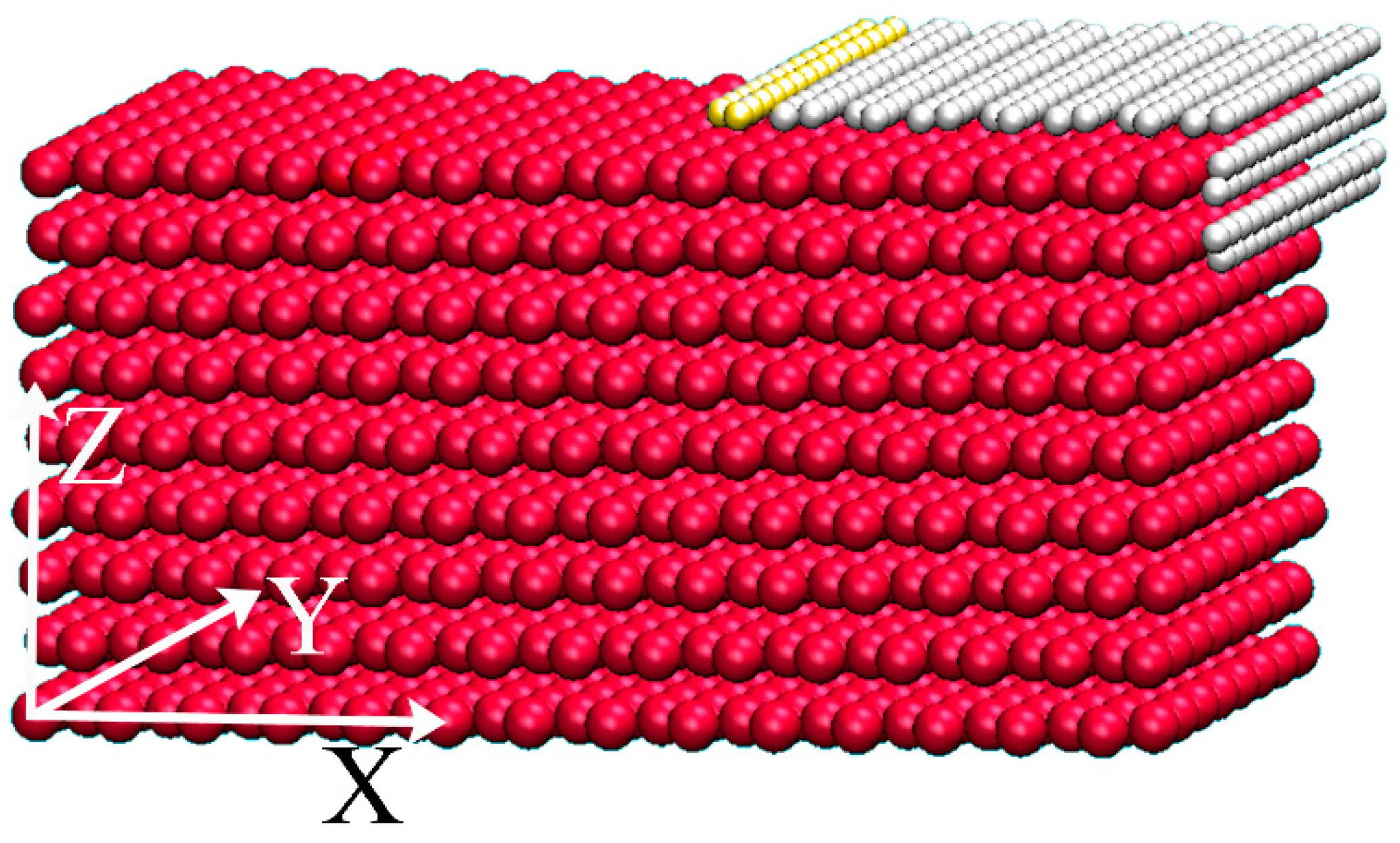
Figure 1. Therefore, we performed MD simulations on the relaxation of a piece of graphene sheet initially stuck to a quarter-turn boundary. Specifically, a Cu substrate of nine atomic layers with (111) surfaces was constructed according to the lattice constant 3.615 Å, and the motion of a graphene sheet containing 290 carbon atoms placed on the quarter-turn boundary was simulated by MD. In the simulation, the carbon atoms of the left-most two rows as well as all the Cu atoms were fixed, and the periodic conditions were applied in the Y-direction. Throughout this work, the standard Verlet algorithm was used to integrate the Newton equation with a time step of 0.2 fs, and the interactions between C-C and Cu-Cu were described by the Brenner function [
10] and the tight-binding potential [
11], respectively, while the interaction between C and Cu atoms was described by the Lennard-Jones (L-J) potential [
12].
Considering that the temperature for graphene growth by CVD is about 1200 K, the C atoms, except for the ones of the left-most two rows (the yellow balls in
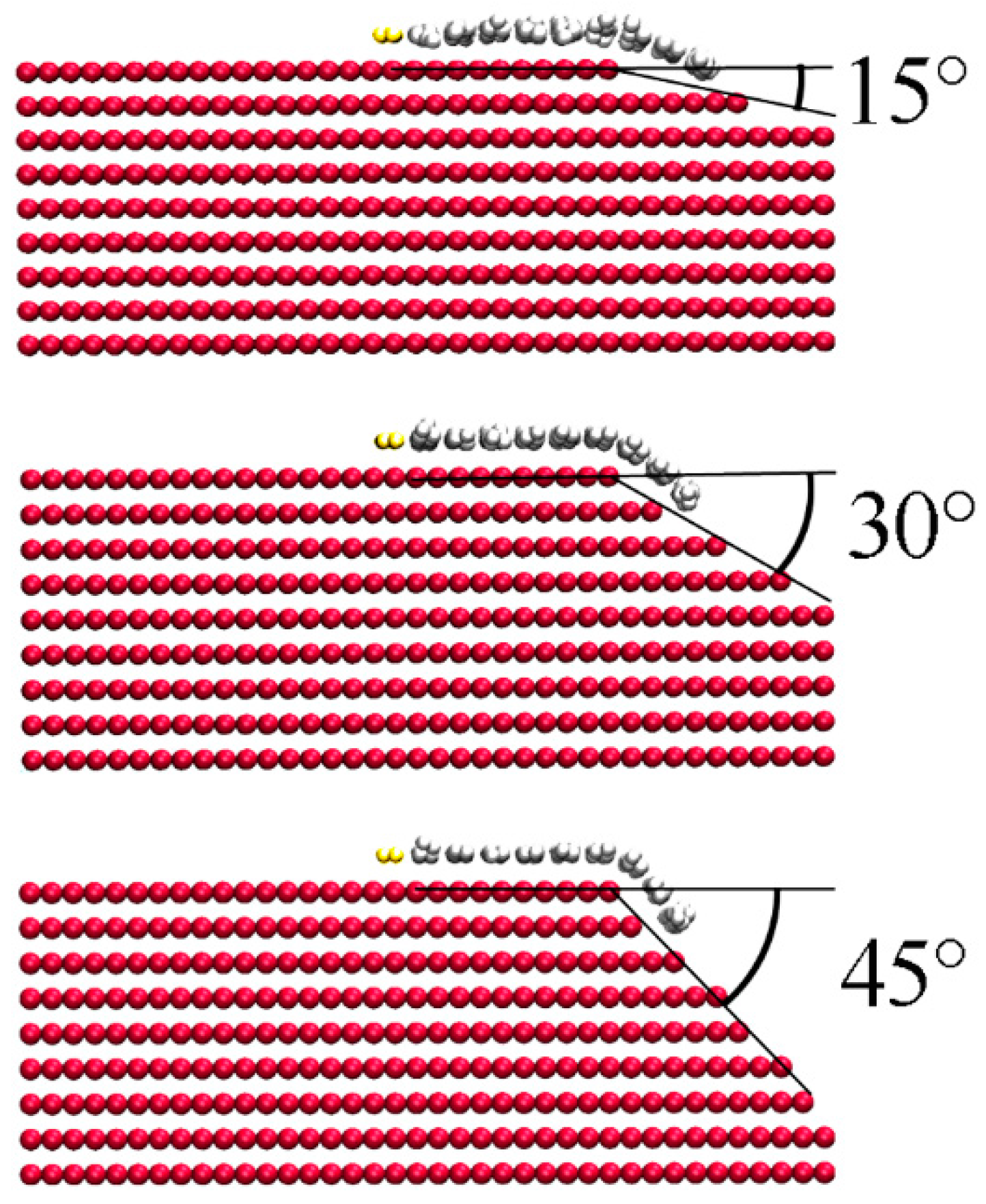
Figure 1), were initially assigned velocities of Maxwell distribution at 1200 K, and were then allowed to relax freely. After about 50 ps, the bent graphene sheet became flat with a little vibration. The initial temperature has little effect on the process. For example, when the mobile C atoms were initially assigned velocities of Maxwell distribution at 300 K, the bent sheet also turned into a flat structure in about 50 ps. However, things changed when the quarter-turn boundary was replaced with a slope of bent angles of 15°, 30°, and 45°, as shown in
Figure 2. After the mobile C atoms were assigned the velocities of Maxwell distribution at 1200 K, the graphene sheet kept the curved shape until the end of the MD simulation, at 200 ps. Nevertheless, we do not know what will happen if the MD simulation can cover a period of more than 1 s, so we have to apply the criterion of GFE to approach this problem.
For zero pressure, the GFE is
where U is the internal energy, and the entropy S is calculated by
where
is the entropy for
0.01 K, and was neglected in this work. The heat capacity
was calculated by
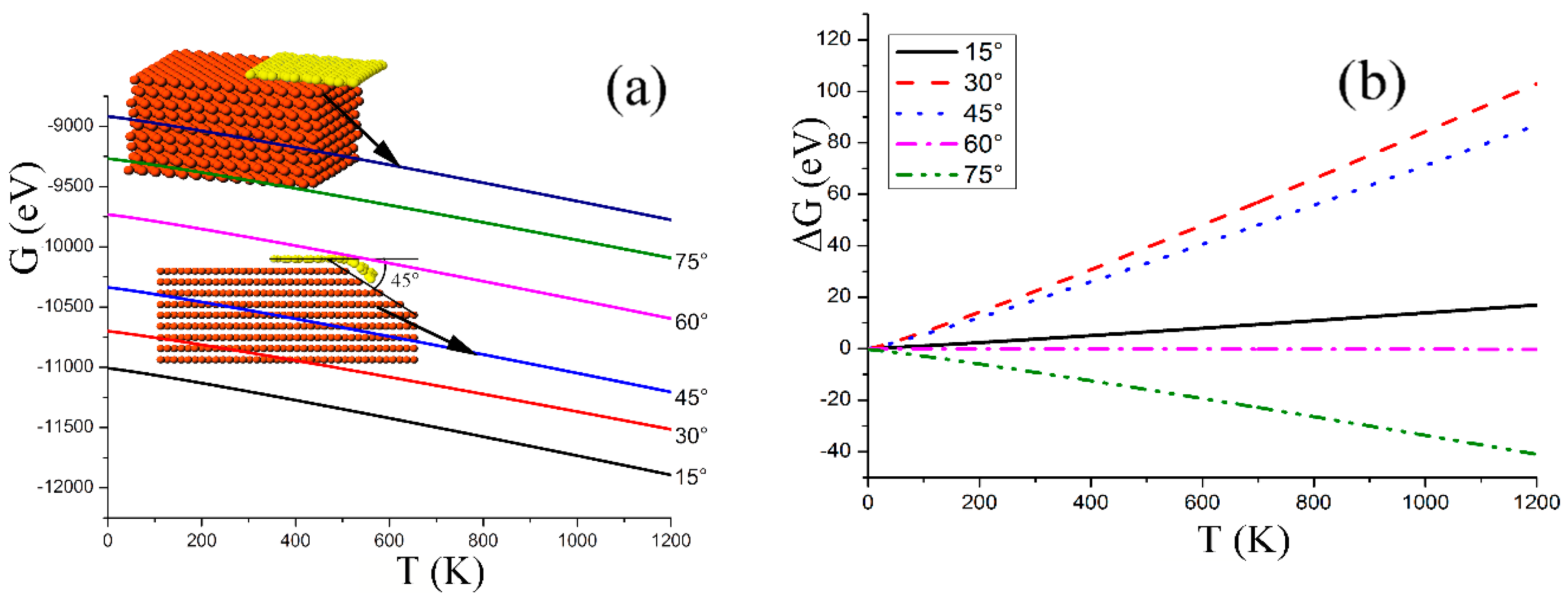
, where the internal energy E as the function of temperature T was obtained by MD simulations. Specifically, the mobile C atoms of the graphene sheet of 290 atoms were first cooled below 0.01 K, and were then assigned velocities of the Maxwell velocity distribution at the temperature T every 0.1 ps until the system reached the prescribed temperature T. Then the system was allowed to relax freely for about 2 ps, during which the internal energy and temperature was recorded every 20 fs to produce the average value. Setting the temperature T from 10 K–40 K with an interval of 10 K, we obtained the relationship between the internal energy and temperature. The obtained GFE of the graphene sheets stuck on the slopes of different angles are shown in
Figure 3a, where the GFE of a flat sheet on a quarter-turn boundary is also presented, indicating that the GFE of the curved graphene on the slopes is significantly smaller than the flat graphene on the quarter-turn boundary, and the smaller the slope angle, the smaller the GFE. For a given slope, the GFE of the flat sheet (
) is significantly larger than for the bent sheet (
) if the slope angle is smaller than 60° (
Figure 3b), indicating that in the process of graphene growth on the Cu surface by CVD, the sheet would stick to the surface of the slopes to form a bent structure as long as the angle is smaller than 60°, and an angle of 30° should be favorable for growth of the bent sheet.
3. SWCNC Growth by CVD Methods
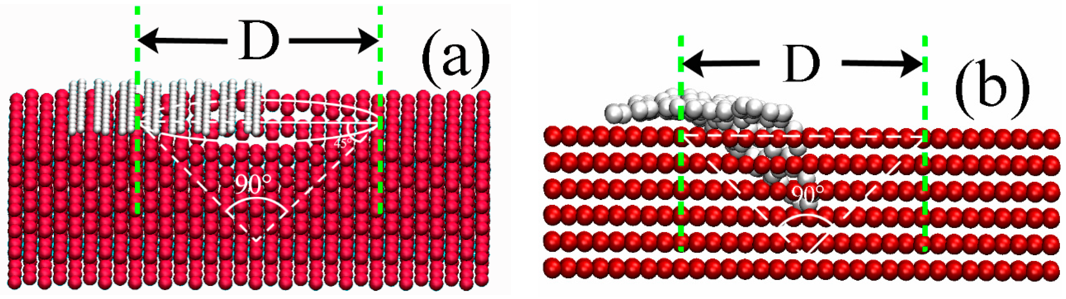
Based on the discussion in the previous section, it is not impossible to grow SWCNCs embedded in graphene sheets by pre-fabricating conical pits on the surface of Cu substrates, and it is necessary to explore the specific conditions for growth. MD simulation seems to be an ideal method to display the growth process and therefore can determine under what conditions SWCNCs may grow on Cu substrates. However, the realistic growth rate of graphene by CVD is too slow for MD to simulate, and we have to resort to the GFE criterion that states for an isobaric process, such as CVD growth, the system tends to a structure of lower GFE. Therefore, we calculated the GFE of a piece of graphene sheet crossing over a pit on the surface (
Figure 4a), or bending into the pit (
Figure 4b), to see which geometry is of smaller GFE.
A technique of time-going-backwards [
13,
14] in the MD simulation was employed to obtain the probable structure of a piece of graphene sheet bent into the pit (
Figure 4b). Specifically, a graphene sheet containing 176 C atoms was initially placed over a conical pit with a 45° angle slope (
Figure 4a), corresponding to a conical angle of 90°, and then the C atoms of the leftmost two rows and all the Cu atoms were kept fixed while the Newton’s equations for the other mobile C atoms were integrated by a negative step of −0.2 fs, during which every mobile C atom was assigned a velocity every 0.16 ps by
where
and
are the present velocity of atom i and the velocity randomly chosen from the Maxwell distribution at 300 K, respectively, while
is a random number (
). In this process, the temperature increased step by step, and when the temperature increased to 4000 K, the Newton’s equations were integrated by a positive step of 0.2 fs and the mobile C atoms were assigned a velocity every 0.16 ps by
When the system arrived at about 300 K, we cooled the system down to 0.01 K by a damping method [
13], and recorded the geometrical structure as well as the potential energy.
The above heating and cooling cycle ran 100 times for each of the conical pits with lower diameters of 1.2, 1.6 or 2.0 nm, producing 100 geometrical structures for each pit. As listed in
Table 1, among the 100 configurations there are 41, 25 and 5 structures extending into the pits with diameters of 2.0, 1.6, and 1.2 nm, respectively, indicating that the larger pits are more favorable to the growth of the bent structures. The potential energy of the resultant structures changes in the range of 30–40 eV, and some of the bent structures have lower potential but others do not, implying that the potential energy is insufficient to judge the dynamic probability for growth of the bent structure.
We calculated the GFE of the above bent structures (
) and of the flat structure (
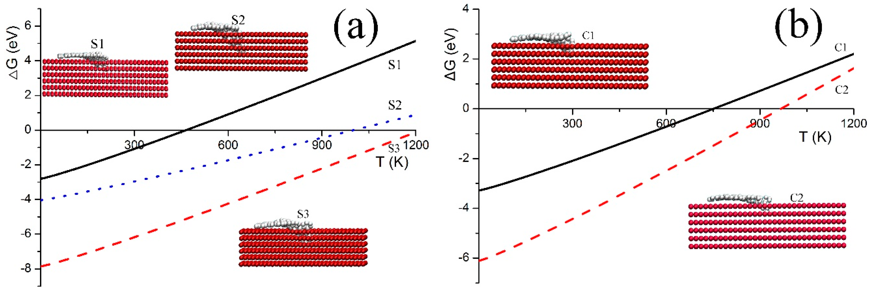
) with the same number of C atoms. The calculations showed, generally, that the lower the potential of the bent structure, the lower the GFE. So only the GFE of the bent structures with lower potential energies need to be inspected. For the pit with a lower diameter of 2.0 nm, three bent structures of lower potential energy denoted by S1, S2 and S3 are shown in the inset in
Figure 5a, where the temperature dependence of the GFE difference, ΔG =
−
, is presented for each of the structures. Below room temperatures, the GFE of the flat sheet is significantly smaller than the bent sheets, while as the temperature increases above 470 K, the GFE of the bent structure S1 gets smaller than the flat sheets. Among the three structures, the GFE of S1 is significantly lower than the others in the entire temperature range (0–1200 K), so at about 1200 K, the CVD growth of graphene on Cu surface should probably be formed. For the pit with a lower diameter of 1.6 nm, two bent structures of lower potential energy, denoted by C1 and C2 in
Figure 5b, have GFEs smaller than the flat structures when the temperature is above 950 K, and the GFE of C1 is significantly smaller in the entire temperature range. Therefore, the bent structure C1 would be more probable in the CVD growth. However, for the pit with a lower diameter of 1.2 nm, the GFEs of all the bent structures are always larger than the flat structures in the temperature range from 0–1200 K, implying that the bent structures can not be formed in this pit.


