
Novel Dilute Bismide, Epitaxy, Physical Properties and Device Application

Abstract
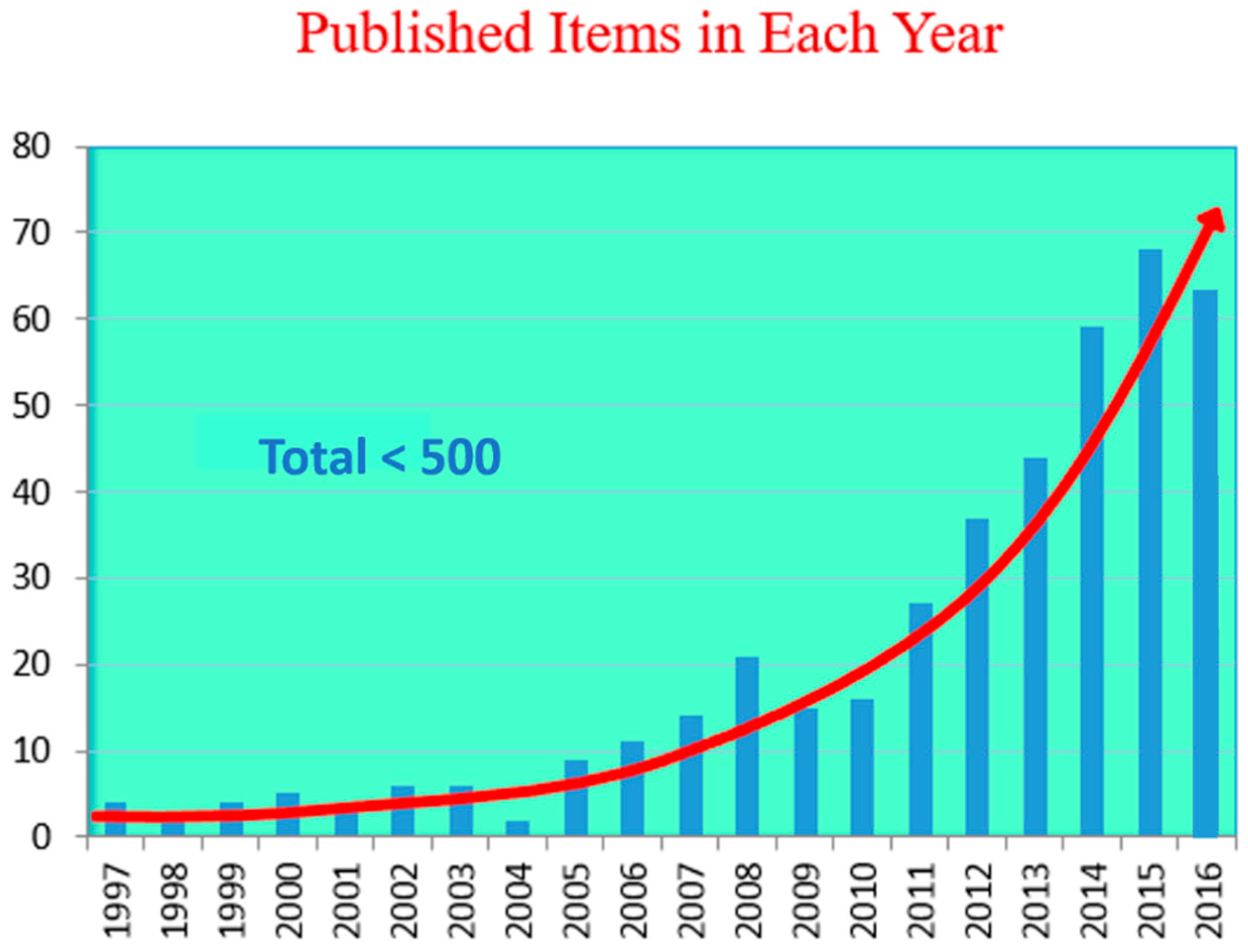
:1. Brief History of Epitaxial Growth of Dilute Bismides
2. Theoretical Prediction
2.1. Empirical Models for Electronic Band Properties
2.1.1. BAC/VBAC Model
2.1.2. TB Model
2.1.3. The k·p Model
2.1.4. Combination of Empirical Models
2.2. Structural, Electronic and Optical Properties Predicted by First Principle Calculations
2.2.1. Structural Property
Thin Films—Binary III-Bi Compounds
GaAs1−xBix
InAs1−xBix and InSb1−xBix
AlN1−xBix
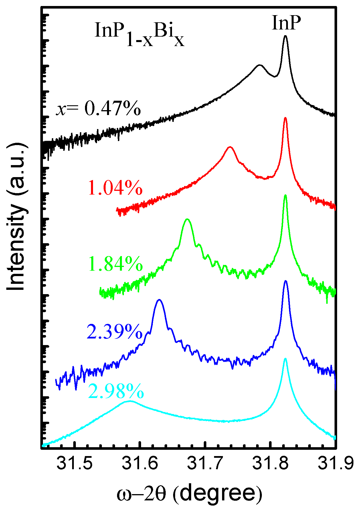
InP1−xBix
Surface
Nanostructures
2.2.2. Electronic and Optical Properties
III-Bi Compound
GaAsBi
GaNBi
AlNBi
2.3. Other Methods
3. Binary Bismides
3.1. Theoretical Predictions
3.2. Growth of Binary III-Bi
4. Epitaxial Growth of GaAsBi
4.1. Bi-Induced Surface Reconstruction, Segregation and Surfactant Effect
4.1.1. Surface Reconstruction
4.1.2. Segregation
4.1.3. Surfactant Effect
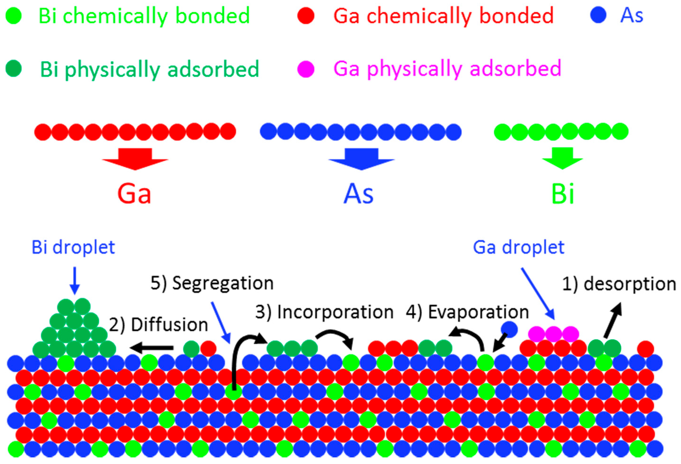
4.2. Bi Surface Droplets, Incorporation and Growth Model
4.2.1. State of Bi Adatoms during Epitaxial Growth
Bi Desorption
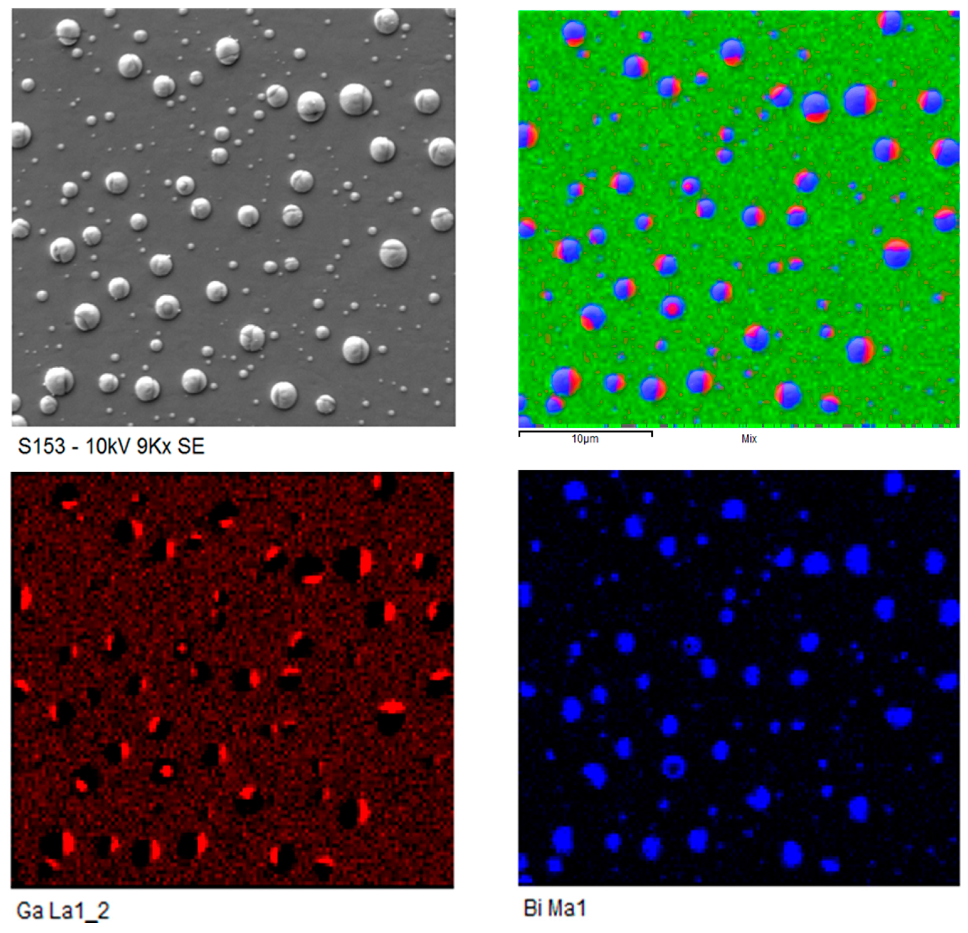
Bi Droplets
Bi Incorporation
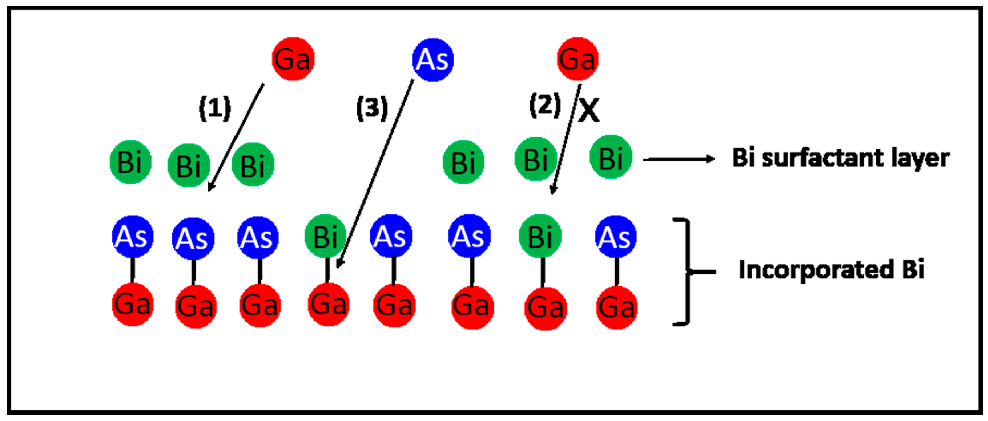
4.2.2. GaAsBi Growth Model
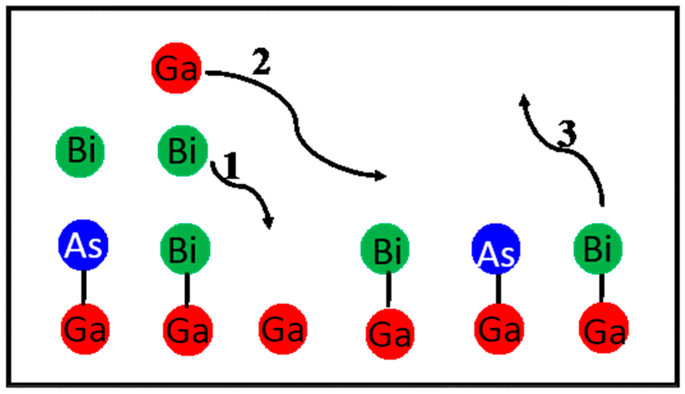
Lu’s GaAsBi Growth Model
Lewis’ GaAsBi Growth Model
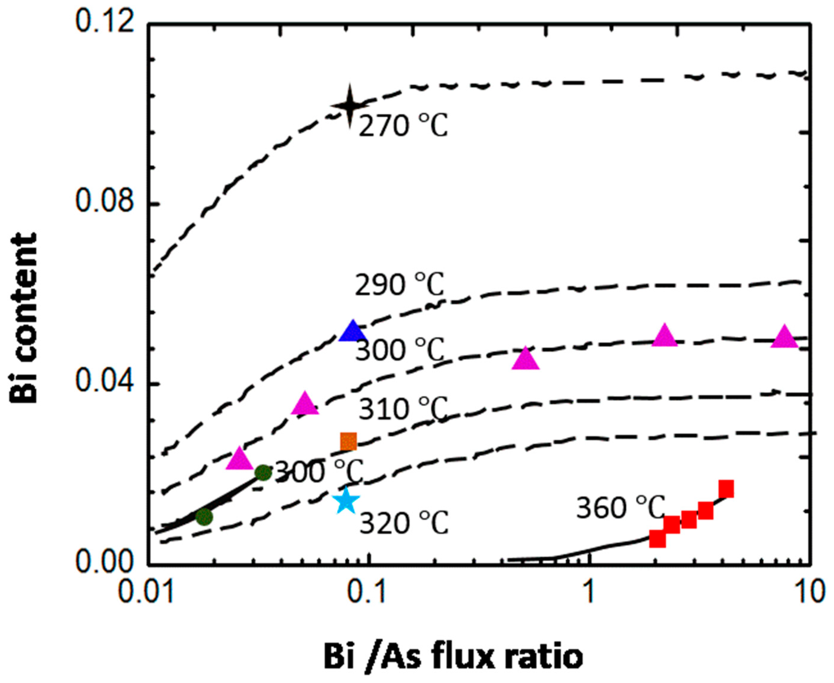
4.3. Influence of Growth Parameters on Bi Incorporation
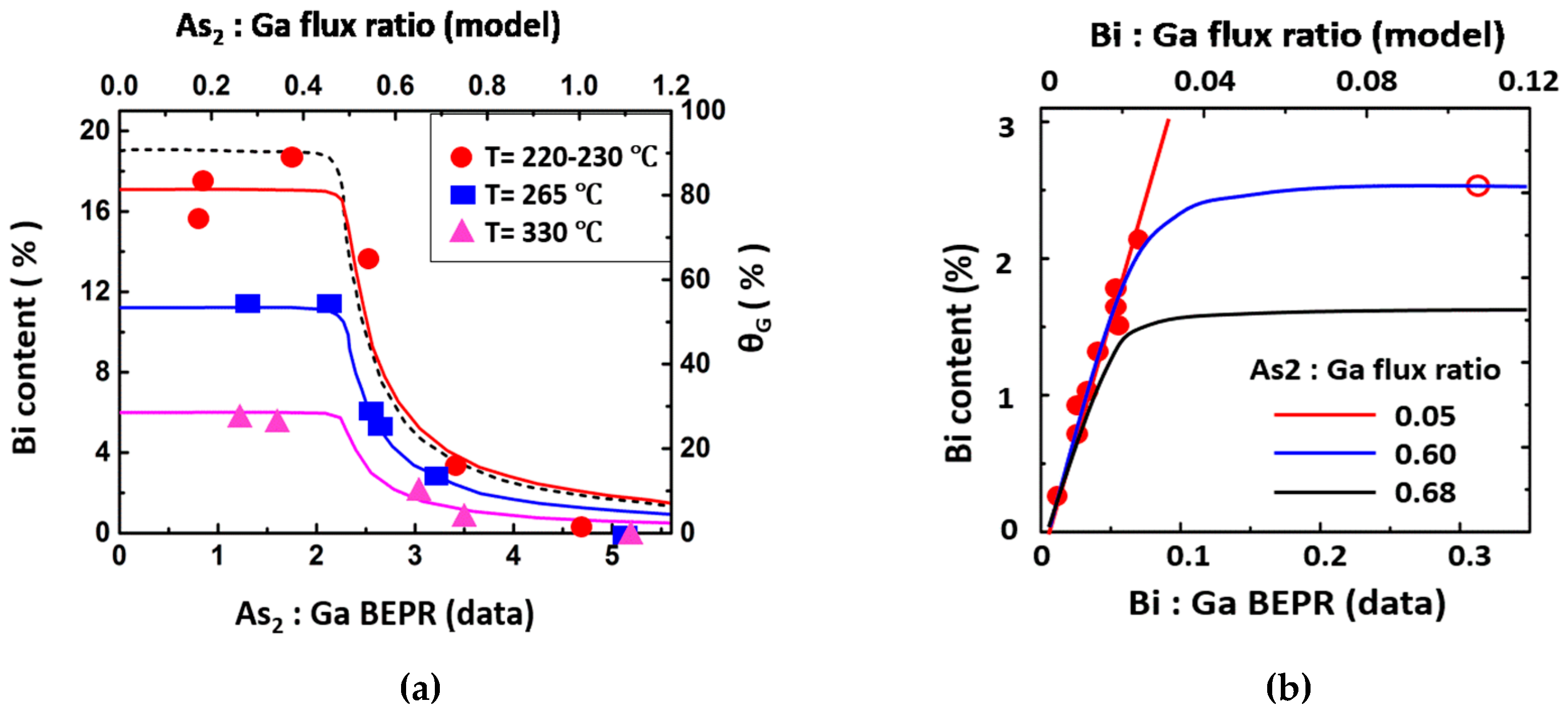
4.3.1. As2:Ga Flux Ratio
4.3.2. Growth Temperature
4.3.3. Bi Flux
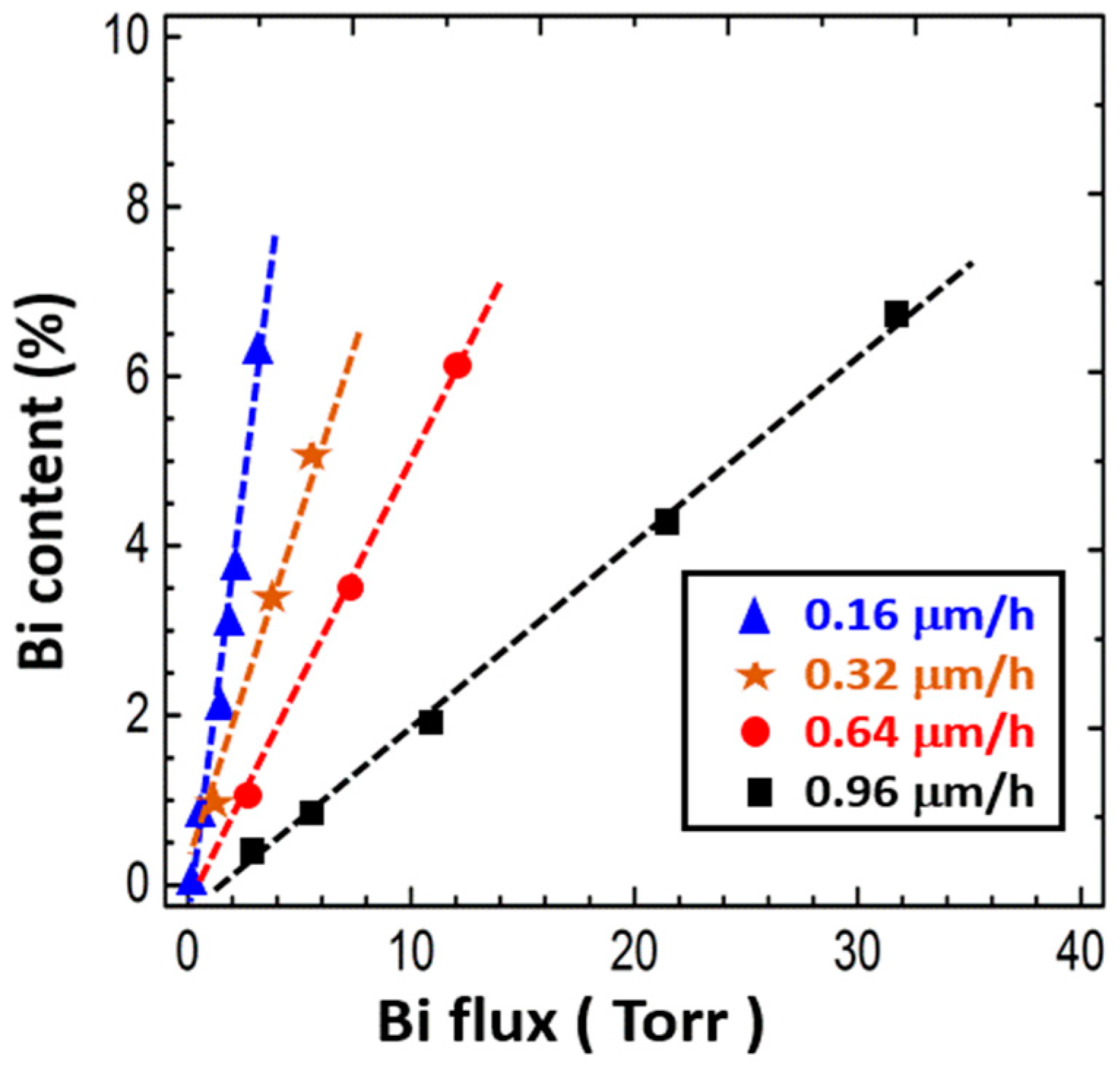
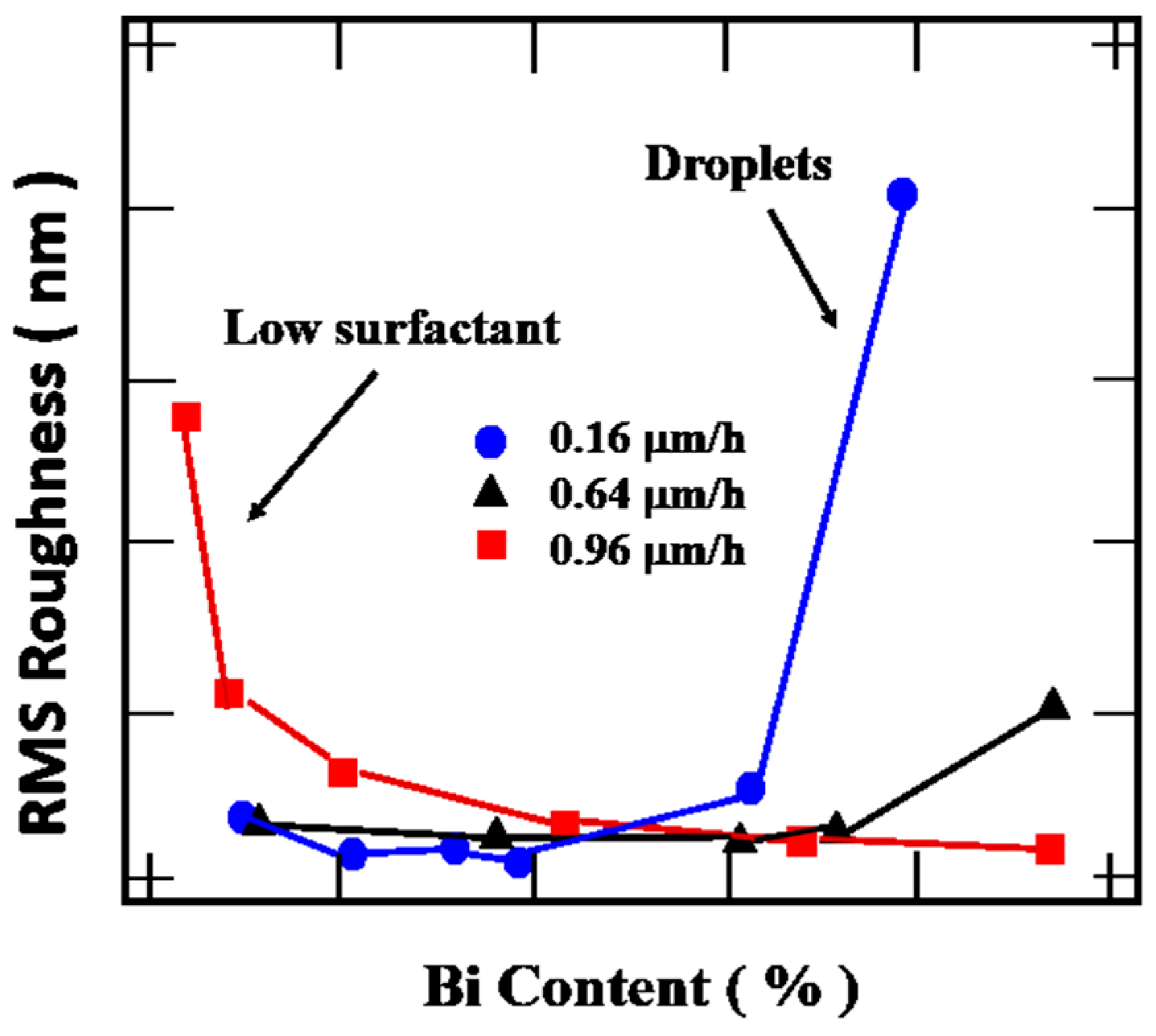
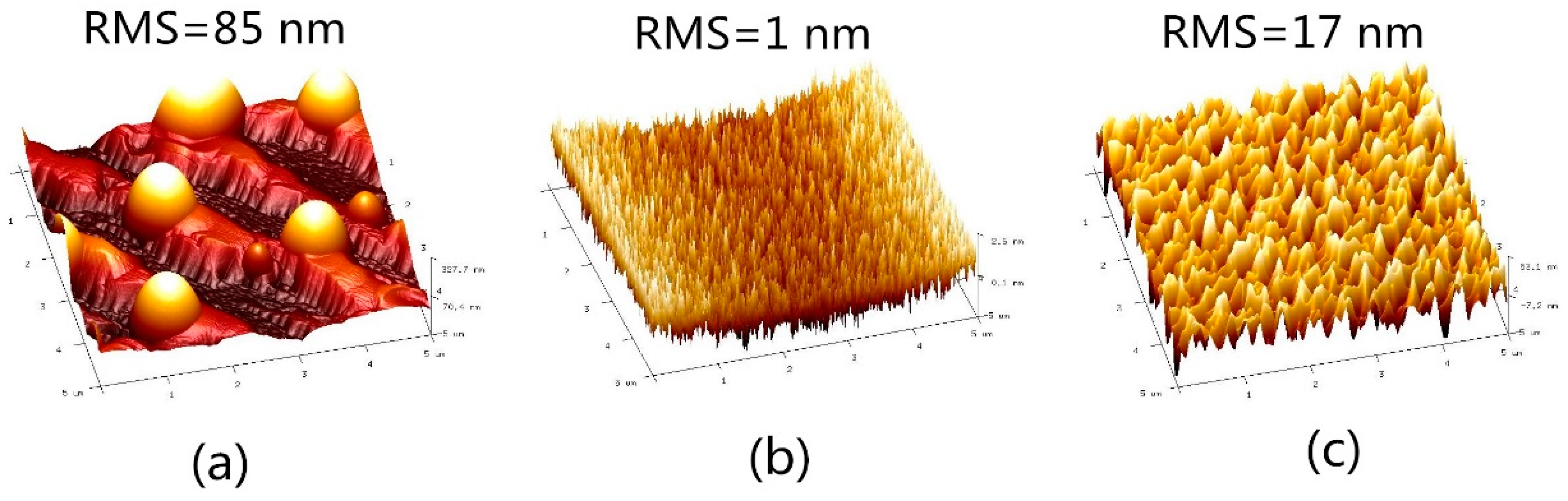
4.3.4. Growth Rate
4.4. Thermal Stability and Bi diffusion
5. Other Dilute Bismides
5.1. III-N-Bi
5.1.1. GaNBi
5.1.2. AlNBi
5.2. III-P-Bi
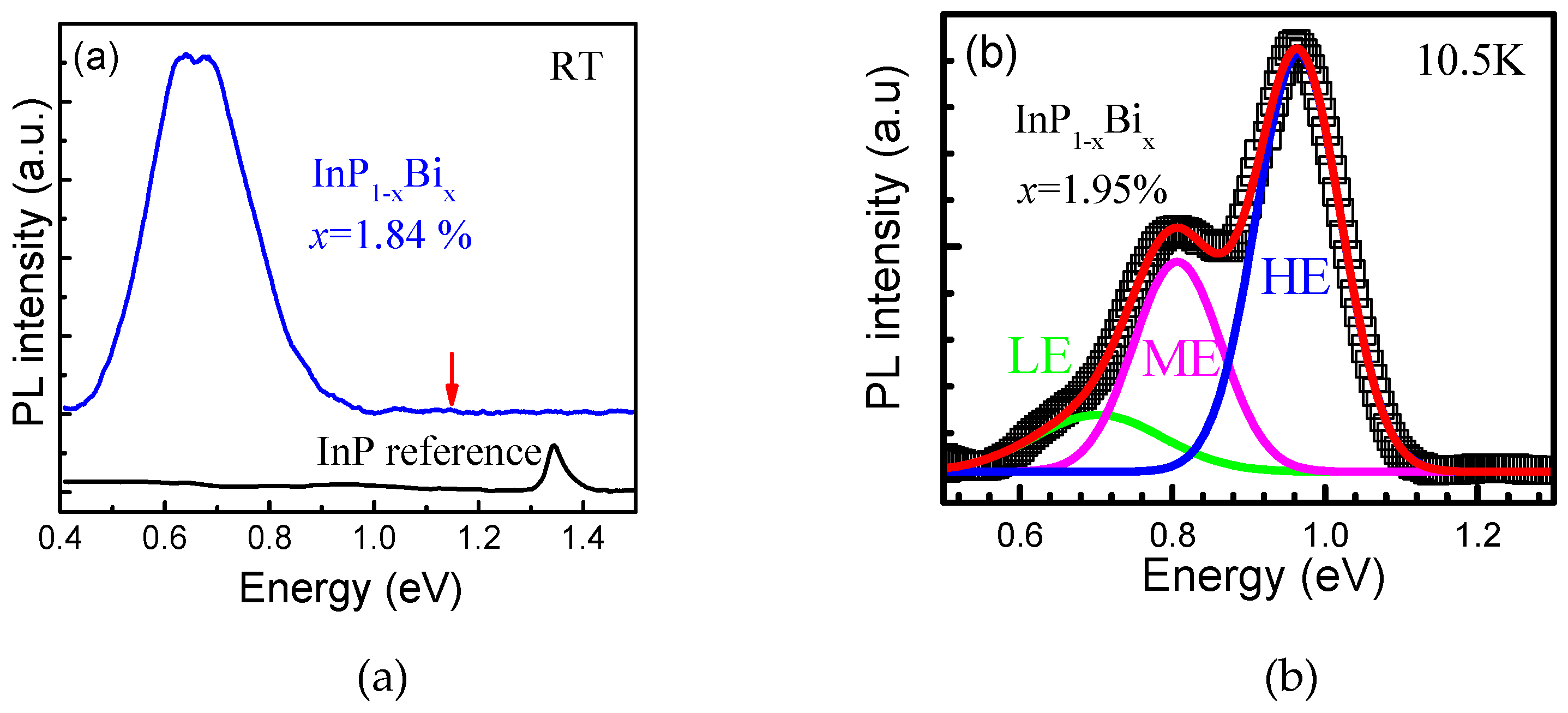
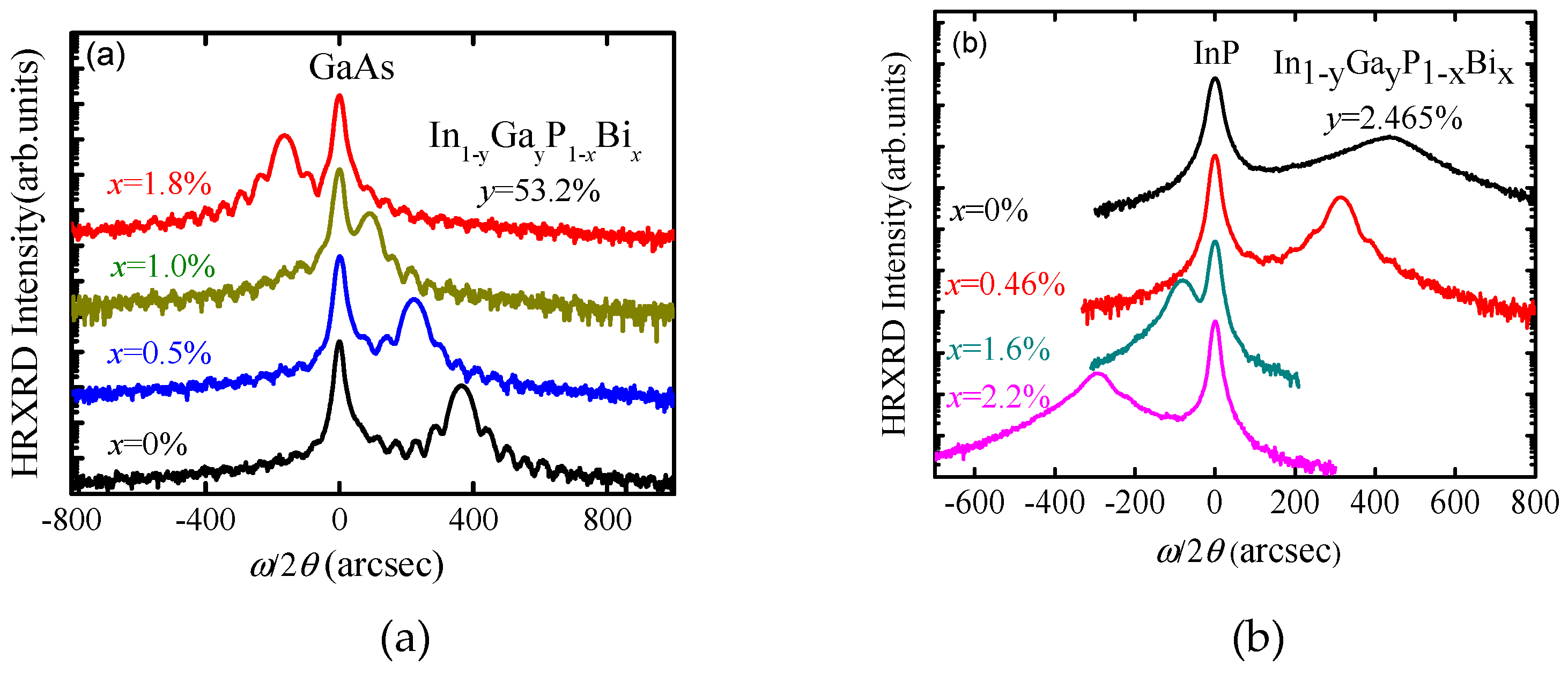
5.2.1. InPBi
Epitaxial Growth
Structure Property
Optical Property
InGaPBi and InAlPBi
N-Bi Co-Doping Phosphides
5.3. III-As-Bi
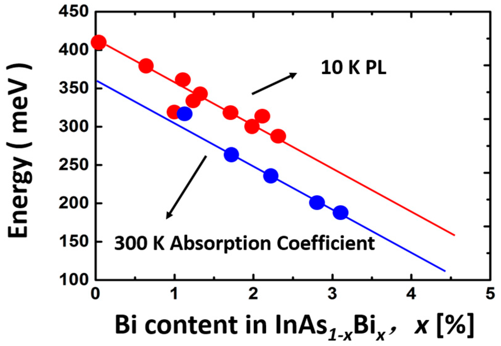
5.3.1. InAsBi
Epitaxial Growth of InAsBi
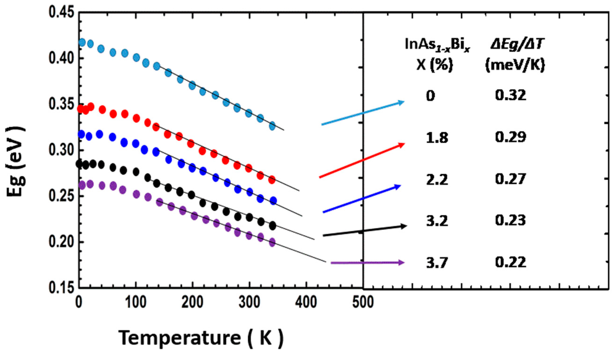
Properties of InAsBi
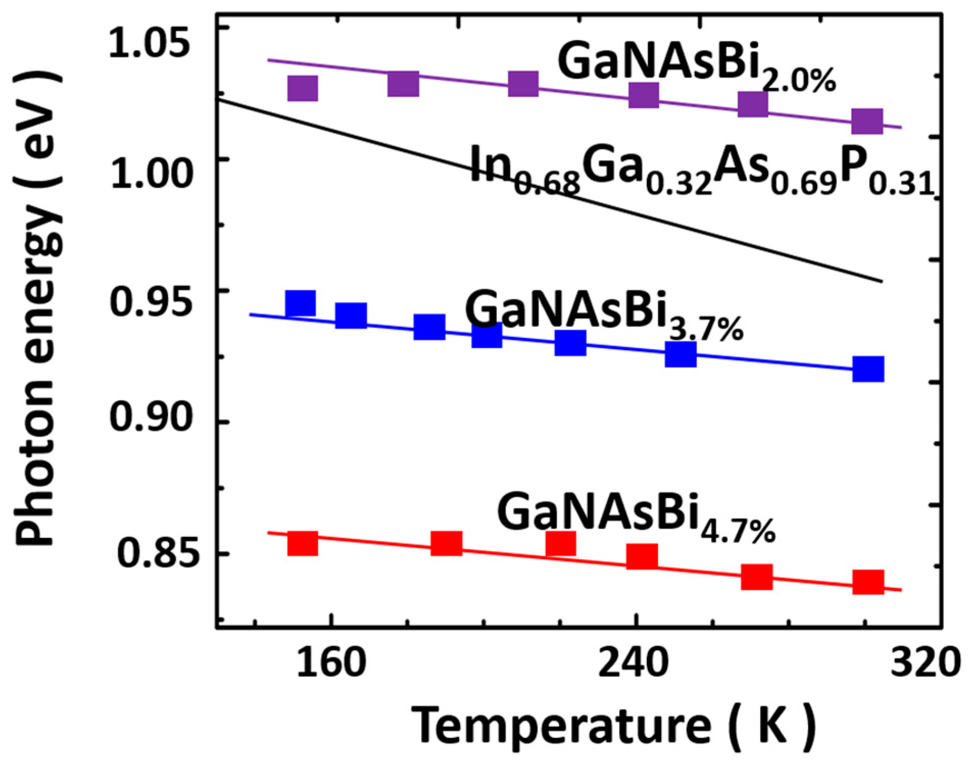
5.3.2. InGaAsBi
Epitaxial Growth of InGaAsBi
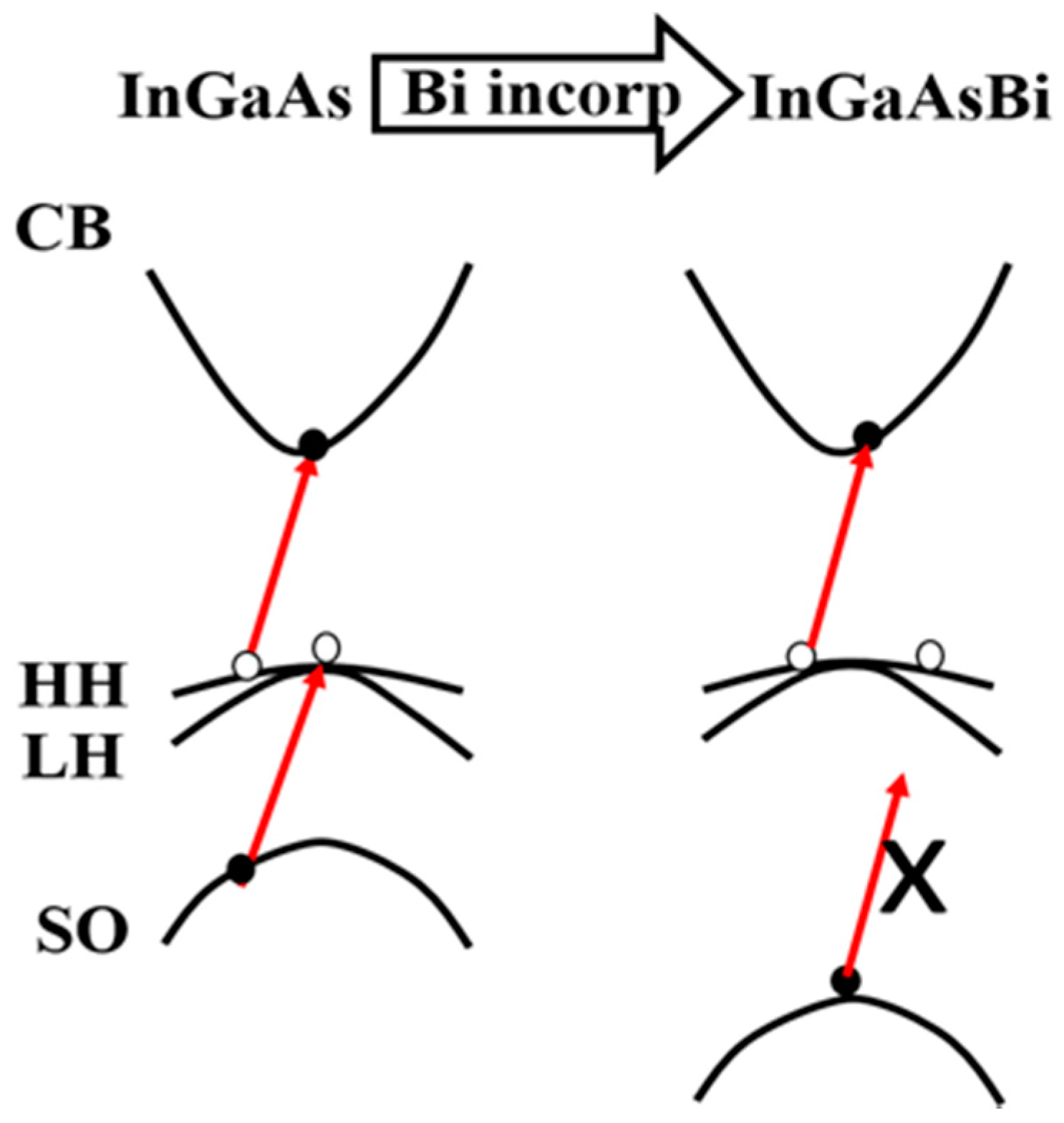
Properties of InGaAsBi
5.4. III-Sb-Bi
5.4.1. InSbBi and Quaternary Alloys
5.4.2. GaSbBi
5.5. Other Quarternary Bismides
5.5.1. GaNAsBi
Epitaxial Growth of GaNAsBi
Properties of GaNAsBi
5.5.2. BGaAsBi
6. Physical Properties of Dilute Bismides
6.1. Surface and Structural Properties
6.1.1. Surfactant Effect and Segregation
6.1.2. Lattice Constant
6.1.3. Lattice Structure
6.2. Electronic and Transport Pproperties, Point Defects
6.2.1. Electronic Properties
6.2.2. Effective Mass
6.2.3. Impact of Alloy Disorder on the Band Structure
6.2.4. Transport Properties
6.2.5. Impurity States
6.3. Optical Properties
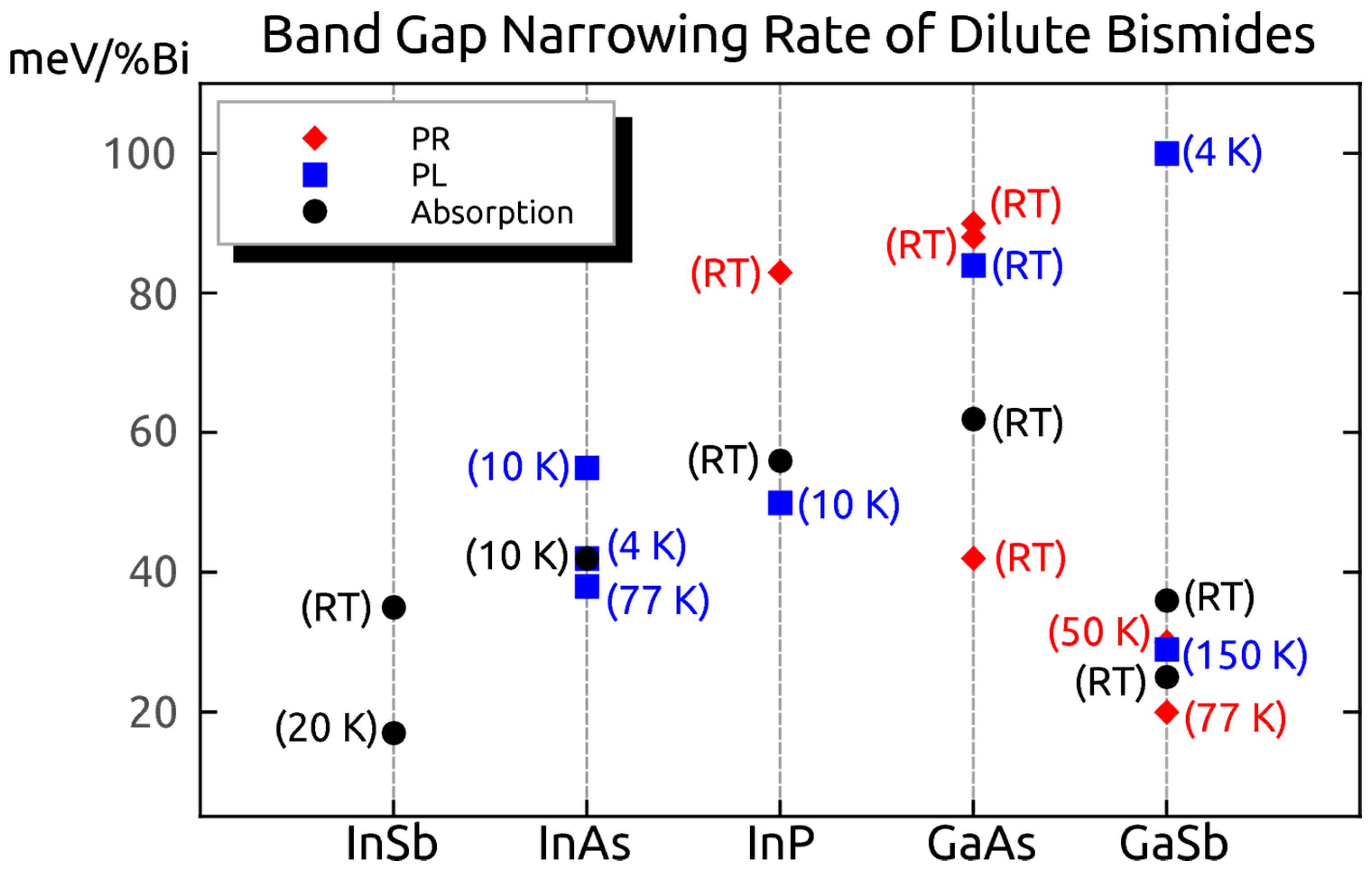
6.3.1. Optical Bandgap
6.3.2. Spectral Broadening in Dilute Bismides
6.3.3. Photoluminescence Intensity
7. Impact of Bismuth on Nanostructures
7.1. Bismuth Surfactant Effect on InAs QDs
7.2. Bismuth Catalyzed Growth of GaAsBi Nanowires
8. Device Application
8.1. Telecom and MIR Lasers
8.2. Photodetectors
8.3. Other Devices
9. Summary
Conflicts of Interest
References
- Bismuth. Available online: https://en.wikipedia.org/wiki/Bismuth (accessed on 16 Feburary 2017).
- Rao, M.L.N.; Shimada, S.; Yamazaki, O.; Tanaka, M. Cross-coupling reaction of organobismuth dialkoxides with aryl bromides and iodides catalyzed by Pd(PPh3)4. J. Organomet. Chem. 2002, 659, 117–120. [Google Scholar] [CrossRef]
- Krabbe, S.W.; Angeles, V.V.; Mohan, R.S. Bismuth (III) bromide in organic synthesis. A catalytic method for the allylation of tetrahydrofuranyl and tetrahydropyranyl ethers. Tetrahedron Lett. 2010, 51, 5643–5645. [Google Scholar] [CrossRef]
- Rohr, O. Bismuth—The new ecologically green metal for modern lubricating engineering. Ind. Lubr. Tribol. 2002, 54, 153–164. [Google Scholar] [CrossRef]
- Binnie, W.P. The structural crystallography of indium bismuthide. Acta Crystallogr. 1956, 9, 686–687. [Google Scholar] [CrossRef]
- Hashimoto, K. Electrical properties of SnTe, SnSe and InBi at low temperatures. J. Phys. Soc. Jpn. 1957, 12, 1423. [Google Scholar] [CrossRef]
- Dietz, R.E.; Thomas, D.G.; Hopfield, J.J. “Mirror” absorption and fluorescence in ZnTe. Phys. Rev. Lett. 1962, 8, 391–393. [Google Scholar] [CrossRef]
- Thomas, D.G.; Hopfield, J.J.; Frosch, C.J. Isoelectronic traps due to nitrogen in gallium phosphide. Phys. Rev. Lett. 1965, 15, 857–860. [Google Scholar] [CrossRef]
- Trumbore, F.A. Luminescence due to the isoelectronic substitution of bismuth for phosphorus in gallium phosphide. Appl. Phys. Lett. 1966, 9, 4–6. [Google Scholar] [CrossRef]
- Dean, P.J.; White, A.M.; Williams, E.W.; Astles, M.G. The isoelectronic trap bismuth in indium phosphide. Solid State Commun. 1971, 9, 1555–1558. [Google Scholar] [CrossRef]
- Armand, V.D. IEEE annals of the history of computing. IEEE Comput. Soc. 2010, 32, 72–79. [Google Scholar]
- Avery, D.G.; Goodwin, D.W.; Lawson, W.D.; Moss, T.S. Optical and photo-electrical properties of indium antimonide. Proc. Phys. Soc. 1954, 67, 761. [Google Scholar] [CrossRef]
- Lawson, W.D.; Nielsen, S.; Putley, E.H.; Young, A.S. Preparation and properties of HgTe and mixed crystals of HgTe-CdTe. J. Phys. Chem. Solids 1959, 9, 325–329. [Google Scholar] [CrossRef]
- Jean-Louis, A.M.; Hamon, C. Propriétés des alliages InSb1−xBix I. mesures électriques. Phys. Status Solidi (b) 1969, 34, 329–340. [Google Scholar] [CrossRef]
- Jean-Louis, A.M.; Ayrault, B.; Vargas, J. Propriétés des alliages InSb1−xBix. II. absorption optique. Phys. Status Solidi (b) 1969, 34, 341–350. [Google Scholar] [CrossRef]
- Joukoff, B.; Jean-Louis, A.M. Growth of InSb1-XBix single-crystals by Czochralski method. J. Cryst. Growth 1972, 12, 169. [Google Scholar] [CrossRef]
- Bugakov, V.L.; Gitsu, D.V.; Dolma, V.A.; Loisher, A.M.; Kotrubenko, B.P.; Laptev, A.V.; Akad, I. Nauk Mold. SSSR Ser. Fiz-Tech. Mat. Nauk 1976, 3, 29. [Google Scholar]
- Velikanova, T.; Turchanin, M.; Lukas, H.L. Bismuth–Indium–Antimony. In Landolt-Bornstein—Group IV Physical Chemistry; Springer: Berlin, Germany, 2007; pp. 168–190. [Google Scholar]
- Zilko, J.L.; Greene, J.E. Growth of metastable InSb1−xBix thin films by multitarget sputtering. Appl. Phys. Lett. 1978, 33, 254–256. [Google Scholar] [CrossRef]
- Zilko, J.L.; Greene, J.E. Growth and phase stability of epitaxial metastable InSb1−xBix films on GaAs. I. Crystal growth. J. Appl. Phys. 1980, 51, 1549–1559. [Google Scholar] [CrossRef]
- Oe, K.; Ando, S.; Sugiyama, K. InSb1-XBix films grown by molecular-beam epitaxy. Jpn. J. Appl. Phys. 1981, 20, L303–L306. [Google Scholar] [CrossRef]
- Noreika, A.J. Indium antimonide-bismuth compositions grown by molecular beam epitaxy. J. Appl. Phys. 1982, 53, 4932–4937. [Google Scholar] [CrossRef]
- Noreika, A.J.; Greggi, J., Jr.; Takei, W.J.; Francombe, M.H. Properties of MBE grown InSb and InSb1−xBix. J. Vac. Sci. Technol. A 1983, 1, 558–561. [Google Scholar] [CrossRef]
- Humphreys, T.P.; Chiang, P.K.; Bedair, S.M.; Parikh, N.R. Metalorganic chemical vapor deposition and characterization of the In-As-Sb-Bi material system for infrared detection. Appl. Phys. Lett. 1988, 53, 142–144. [Google Scholar] [CrossRef]
- Ma, K.Y.; Fang, Z.M.; Jaw, D.H.; Cohen, R.M.; Stringfellow, G.B.; Kosar, W.P.; Brown, D.W. Organometallic vapor phase epitaxial growth and characterization of InAsBi and InAsSbBi. Appl. Phys. Lett. 1989, 55, 2420–2422. [Google Scholar] [CrossRef]
- Ma, K.Y.; Fang, Z.M.; Cohen, R.M.; Stringfellow, G.B. Organometallic vapor-phase epitaxy growth and characterization of Bi-containing III/V alloys. J. Appl. Phys. 1990, 68, 4586–4591. [Google Scholar] [CrossRef]
- Elayech, N.; Fitouri, H.; Essouda, Y.; Rebey, A.; El Jani, B. Thermodynamic study of the ternary system gallium-arsenic-bismuth. Phys. Status Solidi (c) 2015, 12, 138–141. [Google Scholar] [CrossRef]
- Huang, K.T.; Chiu, C.T.; Cohen, R.M.; Stringfellow, G.B. InAsSbBi alloys grown by organometallic vapor-phase epitaxy. J. Appl. Phys. 1994, 75, 2857. [Google Scholar] [CrossRef]
- Wagener, M.C.; Botha, J.R.; Leitch, A.W.R. Characterization of secondary phases formed during MOVPE growth of InSbBi mixed crystals. J. Cryst. Growth 2000, 213, 51–56. [Google Scholar] [CrossRef]
- Lee, J.J.; Kim, J.D.; Razeghi, M. Room temperature operation of 8–12 μm InSbBi infrared photodetectors on GaAs substrates. Appl. Phys. Lett. 1998, 73, 602–604. [Google Scholar] [CrossRef]
- Razeghi, M. Overview of antimonide based III-V semiconductor epitaxial layers and their applications at the center for quantum devices. Eur. Phys. J. Appl. Phys. 2003, 23, 149–205. [Google Scholar] [CrossRef]
- Oe, K.; Okamoto, H. New semiconductor alloy GaAs1-xBix grown by metal organic vapor phase epitaxy. Jpn. J. Appl. Phys. Part 2 1998, 37, L1283–L1285. [Google Scholar] [CrossRef]
- Zinovev, V.; Morgun, A.I.; Ufimtsev, V.B.; Arshavskii, A. Photoluminescence of epitaxial GaAsBi films. Semiconductors 1986, 20, 209–210. [Google Scholar]
- Germogenov, V.P.; Otman, Y.I.; Chaldyshev, V.V. Appearance of natural acceptors in GaSb due to isovalent doping with bismuth. Semiconductors 1990, 24, 689–693. [Google Scholar]
- Chaldyshev, V.V.; Germogenov, V.P.; Shmartsev, Y.V. Photoluminescence of bismuth doped GaSb. Key Eng. Mater. 1992, 65, 109–116. [Google Scholar]
- Gladkov, P.; Monova, E.; Weber, J. Liquid phase epitaxy and photoluminescence characterization of p-type GaSb layers grown from Bi based melts. J. Cryst. Growth 1995, 146, 319–325. [Google Scholar] [CrossRef]
- Mascarenhas, A.; Zhang, Y.; Verley, J.; Seong, M.J. Overcoming limitations in semiconductor alloy design. Superlattices Microstructures 2001, 29, 395–404. [Google Scholar] [CrossRef]
- Weyers, M.; Sato, M.; Ando, H. Red shift of photoluminescence and absorption in dilute GaAsN alloy layers. Jpn. J. Appl. Phys. 1992, 31, L853–L855. [Google Scholar] [CrossRef]
- Baillargeon, J.N.; Cheng, K.Y.; Hofler, G.E.; Pearah, P.J.; Hsieh, K.C. Luminescence quenching and the formation of the GaP1−xNx alloy in GaP with increasing nitrogen content. Appl. Phys. Lett. 1992, 60, 2540–2542. [Google Scholar] [CrossRef]
- Kondow, M.; Uomi, K.; Niwa, A.; Kitatani, T.; Watahiki, S.; Yazawa, Y. GaInNAs: A novel material for long-wavelength-range laser diodes with excellent high-temperature performance. Jpn. J. Appl. Phys. 1996, 35, 1273–1275. [Google Scholar] [CrossRef]
- Kitatani, T.; Nakahara, K.; Kondow, M.; Uomi, K.; Tanaka, T. A 1.3-μm single-quantum-well laser diode with a high characteristic temperature over 200 K. Jpn. J. Appl. Phys. 2000, 39, 86–87. [Google Scholar] [CrossRef]
- Young, D.L.; Geisz, J.F.; Coutts, T.J. Nitrogen-induced decrease of the electron effective mass in GaAs1−xNx thin films measured by thermomagnetic transport phenomena. Appl. Phys. Lett. 2003, 82, 1236–1238. [Google Scholar] [CrossRef]
- Wang, S.M.; Adolfsson, G.; Zhao, H.; Wei, Y.Q.; Gustavsson, J.; Zhao, Q.X.; Sadeghi, M.; Larsson, A. Growth of GaInNAs and 1.3 μm edge emitting lasers by molecular beam epitaxy. J. Cryst. Growth 2009, 311, 1863–1867. [Google Scholar] [CrossRef]
- Tixier, S.; Adamcyk, M.; Tiedje, T.; Francoeur, S.; Mascarenhas, A.; Wei, P.; Schiettekatte, F. Molecular beam epitaxy growth of GaAs1−xBix. Appl. Phys. Lett. 2003, 82, 2245. [Google Scholar] [CrossRef]
- Li, H.; Wang, Z.M. Bismuth-Containing Compounds; Springer: Chengdu, China, 2013. [Google Scholar]
- Carrier, P.; Wei, S.-H. Calculated spin-orbit splitting of all diamondlike and zinc-blende semiconductors: Effects of p1/2 local orbitals and chemical trends. Phys. Rev. B 2004, 70, 035212. [Google Scholar] [CrossRef]
- Fluegel, B.; Francoeur, S.; Mascarenhas, A.; Tixier, S.; Young, E.C.; Tiedje, T. Giant spin-orbit bowing in GaAs1-xBix. Phys. Rev. Lett. 2006, 97, 067205. [Google Scholar] [CrossRef] [PubMed]
- Yoshida, J.; Kita, T.; Wada, O.; Oe, K. Temperature dependence of GaAs1-xBix band gap studied by photoreflectance spectroscopy. Jpn. J. Appl. Phys. 2003, 42, 371–374. [Google Scholar] [CrossRef]
- Hossain, N.; Marko, I.P.; Jin, S.R.; Hild, K.; Sweeney, S.J.; Lewis, R.B.; Beaton, D.A.; Tiedje, T. Recombination mechanisms and band alignment of GaAs1−xBix/GaAs light emitting diodes. Appl. Phys. Lett. 2012, 100, 051105. [Google Scholar] [CrossRef] [Green Version]
- Kini, R.N.; Bhusal, L.; Ptak, A.J.; France, R.; Mascarenhas, A. Electron Hall mobility in GaAsBi. J. Appl. Phys. 2009, 106, 043705. [Google Scholar] [CrossRef]
- Beaton, D.A.; Lewis, R.B.; Masnadi-Shirazi, M.; Tiedje, T. Temperature dependence of hole mobility in GaAs1−xBix alloys. J. Appl. Phys. 2010, 108, 083708. [Google Scholar] [CrossRef]
- Pillai, M.R.; Kim, S.S.; Ho, S.T.; Barnett, S.A. Growth of InxGa1-xAs/GaAs heterostructures using Bi as a surfactant. J. Vac. Sci. Technol. B 2000, 18, 1232–1236. [Google Scholar] [CrossRef]
- Sweeney, S.J.; Jin, S.R. Bismide-nitride alloys: Promising for efficient light emitting devices in the near- and mid-infrared. J. Appl. Phys. 2013, 113, 043110. [Google Scholar] [CrossRef]
- Ludewig, P.; Knaub, N.; Hossain, N.; Reinhard, S.; Nattermann, L.; Marko, I.P.; Jin, S.R.; Hild, K.; Chatterjee, S.; Stolz, W.; et al. Electrical injection Ga(AsBi)/(AlGa)As single quantum well laser. Appl. Phys. Lett. 2013, 102, 242115. [Google Scholar] [CrossRef] [Green Version]
- Vurgaftman, I.; Meyer, J.R.; Ram-Mohan, L.R. Band parameters for III–V compound semiconductors and their alloys. J. Appl. Phys. 2001, 89, 5815. [Google Scholar] [CrossRef]
- Smith, D.L.; Mailhiot, C. Theory of semiconductor superlattice electronic structure. Rev. Modern Phys. 1990, 62, 173–234. [Google Scholar] [CrossRef]
- Burt, M.G. The justification for applying the effective-mass approximation to microstructures. J. Phys.-Condens. Matter 1992, 4, 6651–6690. [Google Scholar] [CrossRef]
- Broderick, C.A.; Usman, M.; Sweeney, S.J.; O’Reilly, E.P. Band engineering in dilute nitride and bismide semiconductor lasers. Semicond. Sci. Technol. 2012, 27, 094011. [Google Scholar] [CrossRef]
- Alberi, K.; Dubon, O.D.; Walukiewicz, W.; Yu, K.M.; Bertulis, K.; Krotkus, A. Valence band anticrossing in GaBixAs1−x. Appl. Phys. Lett. 2007, 91, 051909. [Google Scholar] [CrossRef]
- Deng, H.-X.; Li, J.; Li, S.-S.; Peng, H.; Xia, J.-B.; Wang, L.-W.; Wei, S.-H. Band crossing in isovalent semiconductor alloys with large size mismatch: First-principles calculations of the electronic structure of Bi and N incorporated GaAs. Phys. Rev. B 2010, 82, 193204. [Google Scholar] [CrossRef]
- Jin, S.; Sweeney, S.J. InGaAsBi alloys on InP for efficient near- and mid-infrared light emitting devices. J. Appl. Phys. 2013, 114, 213103. [Google Scholar] [CrossRef]
- Petropoulos, J.P.; Zhong, Y.; Zide, J.M.O. Optical and electrical characterization of InGaBiAs for use as a mid-infrared optoelectronic material. Appl. Phys. Lett. 2011, 99, 031110. [Google Scholar] [CrossRef]
- Batool, Z.; Hild, K.; Hosea, T.J.C.; Lu, X.; Tiedje, T.; Sweeney, S.J. The electronic band structure of GaBiAs/GaAs layers: Influence of strain and band anti-crossing. J. Appl. Phys. 2012, 111, 113108. [Google Scholar] [CrossRef] [Green Version]
- Marko, I.P.; Batool, Z.; Hild, K.; Jin, S.R.; Hossain, N.; Hosea, T.J.C.; Petropoulos, J.P.; Zhong, Y.; Dongmo, P.B.; Zide, J.M.O.; et al. Temperature and Bi-concentration dependence of the bandgap and spin-orbit splitting in InGaBiAs/InP semiconductors for mid-infrared applications. Appl. Phys. Lett. 2012, 101, 221108. [Google Scholar] [CrossRef] [Green Version]
- Wu, L.Y.; Han, L.H.; Li, X.Y.; Lu, P.F.; Wang, S.M. Asia Communications and Photonics Conference (ACP 2015); Hong Kong, China, November 19–23 2015; OSA publishing: Washington, DC, USA, 2015; ASu2A. 16. [Google Scholar]
- Samajdar, D.P.; Dhar, S. Valence band structure of InAs1-xBix and InSb1-xBix alloy semiconductors calculated using valence band anticrossing model. Sci. World J. 2014, 2014, 704830. [Google Scholar] [CrossRef] [PubMed]
- Usman, M.; Broderick, C.A.; Lindsay, A.; O’Reilly, E.P. Tight-binding analysis of the electronic structure of dilute bismide alloys of GaP and GaAs. Phys. Rev. B 2011, 84, 245202. [Google Scholar] [CrossRef]
- Virkkala, V.; Havu, V.; Tuomisto, F.; Puska, M.J. Modeling Bi-induced changes in the electronic structure of GaAs1−xBix alloys. Phys. Rev. B 2013, 88, 235201. [Google Scholar] [CrossRef]
- Usman, M.; Broderick, C.A.; Batool, Z.; Hild, K.; Hosea, T.J.C.; Sweeney, S.J.; O’Reilly, E.P. Impact of alloy disorder on the band structure of compressively strained GaBixAs1−x. Phys. Rev. B 2013, 87, 115104. [Google Scholar] [CrossRef]
- Fluegel, B.; Kini, R.N.; Ptak, A.J.; Beaton, D.; Alberi, K.; Mascarenhas, A. Shubnikov-de Haas measurement of electron effective mass in GaAs1−xBix. Appl. Phys. Lett. 2011, 99, 162108. [Google Scholar] [CrossRef]
- Lindsay, A.; Tomić, S.; O’Reilly, E.P. Derivation of a 10-band model for dilute nitride semiconductors. Solid State Electron. 2003, 47, 443–446. [Google Scholar] [CrossRef]
- Broderick, C.A.; Usman, M.; O’Reilly, E.P. 12-band k·p model for dilute bismide alloys of (In)GaAs derived from supercell calculations. Phys. Status Solidi (b) 2013, 250, 773–778. [Google Scholar] [CrossRef]
- Broderick, C.A.; Usman, M.; O’Reilly, E.P. Derivation of 12- and 14-band k·p Hamiltonians for dilute bismide and bismide-nitride semiconductors. Semicond. Sci. Technol. 2013, 28, 125025. [Google Scholar] [CrossRef]
- Samajdar, D.P.; Das, T.D.; Dhar, S. Calculation of direct E0 energy gaps for III-V-Bi alloys using quantum dielectric theory. In The Book Physics of Semiconductor Devices; Springer International Publishing: Cham, Switzerland, 2014; pp. 779–781. [Google Scholar]
- Belabbes, A.; Zaoui, A.; Ferhat, M. Lattice dynamics study of bismuth III–V compounds. J. Phys. 2008, 20, 415221. [Google Scholar] [CrossRef]
- Madouri, D.; Ferhat, M. How do electronic properties of conventional III-V semiconductors hold for the III-V boron bismuth BBi compound? Phys. Status Solidi (b) 2005, 242, 2856–2863. [Google Scholar] [CrossRef]
- Reshak, A.H.; Kamarudin, H.; Auluck, S.; Kityk, I.V. Bismuth in gallium arsenide: Structural and electronic properties of GaAs1−xBix alloys. J. Solid State Chem. 2012, 186, 47–53. [Google Scholar] [CrossRef]
- Abdiche, A.; Abid, H.; Riane, R.; Bouaza, A. Structural and electronic properties of zinc blend GaAs1−xBix solid solutions. Physica B 2010, 405, 2311–2316. [Google Scholar] [CrossRef]
- Jacobsen, H.; Puchala, B.; Kuech, T.F.; Morgan, D. Ab initio study of the strain dependent thermodynamics of Bi doping in GaAs. Phys. Rev. B 2012, 86, 085207. [Google Scholar] [CrossRef]
- Berding, M.A.; Sher, A.; Chen, A.B.; Miller, W.E. Structural properties of bismuth-bearing semiconductor alloys. J. Appl. Phys. 1988, 63, 107–115. [Google Scholar] [CrossRef]
- Mbarki, M.; Alaya, R.; Rebey, A. Ab initio investigation of structural and electronic properties of zinc blende AlN1−xBix alloys. Solid State Commun. 2013, 155, 12–15. [Google Scholar] [CrossRef]
- Mbarki, M.; Rebey, A. First principles calculations of structural and electronic properties of GaN1−xBix alloys. J. Alloys Compd. 2012, 530, 36–39. [Google Scholar] [CrossRef]
- Wu, L.; Lu, P.; Yang, C.; Liang, D.; Zhang, C.; Wang, S. The effect of BiIn hetero-antisite defects in In1–xPBix alloy. J. Alloys Compd. 2016, 674, 21–25. [Google Scholar] [CrossRef]
- Punkkinen, M.P.J.; Laukkanen, P.; Komsa, H.P.; Ahola-Tuomi, M.; Räsänen, N.; Kokko, K.; Kuzmin, M.; Adell, J.; Sadowski, J.; Perälä, R.E.; et al. Bismuth-stabilized (2 × 1) and (2 × 4) reconstructions on GaAs(100) surfaces: Combined first-principles, photoemission, and scanning tunneling microscopy study. Phys. Rev. B 2008, 78, 195304. [Google Scholar] [CrossRef]
- Murase, I.; Akiyama, T.; Nakamura, K.; Ito, T. Ab initio-based approach to initial incorporation of Bi on GaAs (001)-c(4 × 4) α surface. J. Cryst. Growth 2013, 378, 21–24. [Google Scholar] [CrossRef]
- Achour, H.; Louhibi, S.; Amrani, B.; Tebboune, A.; Sekkal, N. Structural and electronic properties of GaAsBi. Superlattices Microstructures 2008, 44, 223–229. [Google Scholar] [CrossRef]
- Qi, J.S.; Shi, D.S.; Zhao, J.J.; Jiang, X.F. Stable structures and electronic properties of the oriented Bi nanowires and nanotubes from first-principle calculations. J. Phys. Chem. 2008, 112, 10745–10753. [Google Scholar] [CrossRef]
- Gupta, U.; Reveles, J.U.; Melko, J.J.; Khanna, S.N.; Castleman, A.W., Jr. Electron delocalization in a non-cyclic all-metal III–V cluster. Chem. Phys. Lett. 2009, 480, 189–192. [Google Scholar] [CrossRef]
- Gupta, U.; Reveles, J.U.; Melko, J.J.; Khanna, S.N.; Castleman, A.W., Jr. Electronic structure of Bi3Gay semiconductor clusters and the special stability of Bi3Ga2—A gas phase Zintl analogue. Chem. Phys. Lett. 2009, 467, 223–229. [Google Scholar] [CrossRef]
- Gupta, U.; Reveles, J.U.; Melko, J.J.; Khanna, S.N.; Castleman, A.W., Jr. Origins of stability in mixed bismuth-indium clusters. J. Phys. Chem. C 2010, 114, 15963–15972. [Google Scholar] [CrossRef]
- Akola, J.; Atodiresei, N.; Kalikka, J.; Larrucea, J.; Jones, R.O. Structure and dynamics in liquid bismuth and Bi(n) clusters: A density functional study. J. Chem. Phys. 2014, 141, 194503. [Google Scholar] [CrossRef] [PubMed]
- Amrani, B.; Achour, H.; Louhibi, S.; Tebboune, A.; Sekkal, N. First principles study of AlBi. Solid State Commun. 2008, 148, 59–62. [Google Scholar] [CrossRef]
- Mbarki, M.; Rebey, A. First-principles calculation of the physical properties of GaAs1-xBix alloys. Semicond. Sci. Technol. 2011, 26, 105020. [Google Scholar] [CrossRef]
- Ding, L.; Lu, P.; Cao, H.; Cai, N.; Yu, Z.; Gao, T.; Wang, S. Bismuth alloying properties in GaAs nanowires. J. Solid State Chem. 2013, 205, 44–48. [Google Scholar] [CrossRef]
- Belabbes, A.; Zaoui, A.; Laref, S.; Ferhat, M. Imposing changes of band and spin–orbit gaps in GaNBi. Solid State Commun. 2012, 152, 1700–1702. [Google Scholar] [CrossRef]
- Madouri, D.; Boukra, A.; Zaoui, A.; Ferhat, M. Bismuth alloying in GaAs: A first-principles study. Comput. Mater. Sci. 2008, 43, 818–822. [Google Scholar] [CrossRef]
- Yu, L.; Li, D.; Zhao, S.; Li, G.; Yang, K. First principles study on electronic structure and optical properties of ternary GaAs:Bi alloy. Materials 2012, 5, 2486–2497. [Google Scholar] [CrossRef]
- Nikulin, V.K.; Guschina, N.A. Single-electron charge transfer and excitations at collisions between Bi4+ ions in the kiloelectronvolt energy range. Tech. Phys. 2007, 52, 148–158. [Google Scholar] [CrossRef]
- Dai, J.; Manson, J.R. Theoretical analysis for the determination of surface composition in molten Ga-Bi metal alloys by rare gas scattering. J. Chem. Phys. 2003, 119, 9842. [Google Scholar] [CrossRef]
- Imhof, S.; Wagner, C.; Chernikov, A.; Koch, M.; Kolata, K.; Köster, N.S.; Chatterjee, S.; Koch, S.W.; Lu, X.; Johnson, S.R.; et al. Evidence of two disorder scales in Ga(AsBi). Phys. Status Solidi (b) 2011, 248, 851–854. [Google Scholar] [CrossRef]
- Keen, B.; Makin, R.; Stampe, P.A.; Kennedy, R.J.; Sallis, S.; Piper, L.J.; McCombe, B.; Durbin, S.M. Growth parameters for thin film InBi grown by molecular beam epitaxy. J. Electron. Mater. 2014, 43, 914–920. [Google Scholar] [CrossRef]
- Ferhat, M.; Zaoui, A. Structural and electronic properties of III-V bismuth compounds. Phys. Rev. B 2006, 73, 115107. [Google Scholar] [CrossRef]
- Wang, S.Q.; Ye, H.Q. Plane-wave pseudopotential study on mechanical and electronic properties for IV and III-V crystalline phases with zinc-blende structure. Phys. Rev. B 2002, 66, 235111. [Google Scholar] [CrossRef]
- Zaoui, A.; Madouri, D.; Ferhat, M. First-principles study of the ground state stability of III–V bismuth compounds. Philos. Mag. Lett. 2009, 89, 807–813. [Google Scholar] [CrossRef]
- Duzik, A.; Thomas, J.C.; Millunchick, J.M.; Lång, J.; Punkkinen, M.P.J.; Laukkanen, P. Surface structure of bismuth terminated GaAs surfaces grown with molecular beam epitaxy. Surf. Sci. 2012, 606, 1203–1207. [Google Scholar] [CrossRef]
- Masnadi-Shirazi, M.; Beaton, D.A.; Lewis, R.B.; Lu, X.; Tiedje, T. Surface reconstructions during growth of GaAs1−xBix alloys by molecular beam epitaxy. J. Cryst. Growth 2012, 338, 80–84. [Google Scholar] [CrossRef]
- Norman, A.G.; France, R.; Ptak, A.J. Atomic ordering and phase separation in MBE GaAs1−xBix. J. Vac. Sci. Technol. B 2011, 29, 03C121. [Google Scholar] [CrossRef]
- Ahola-Tuomi, M.; Laukkanen, P.; Perälä, R.E.; Kuzmin, M.; Pakarinen, J.; Väyrynen, I.J.; Adell, M. Structural properties of Bi-terminated GaAs (001) surface. Surf. Sci. 2006, 600, 2349–2354. [Google Scholar] [CrossRef]
- Bastiman, F.; Cullis, A.G.; David, J.P.R.; Sweeney, S.J. Bi incorporation in GaAs(100)-2 × 1 and 4 × 3 reconstructions investigated by RHEED and STM. J. Cryst. Growth 2012, 341, 19–23. [Google Scholar] [CrossRef]
- Wu, M.; Luna, E.; Puustinen, J.; Guina, M.; Trampert, A. Formation and phase transformation of Bi-containing QD-like clusters in annealed GaAsBi. Nanotechnology 2014, 25, 205605. [Google Scholar] [CrossRef] [PubMed]
- Morgan, J.A.; Nathanson, G.M. Atom scattering from atomic surfactants: Collisions of argon with a dilute Bi:Ga solution. J. Chem. Phys. 2001, 114, 1958–1961. [Google Scholar] [CrossRef]
- Fan, D.; Zeng, Z.; Dorogan, V.G.; Hirono, Y.; Li, C.; Mazur, Y.I.; Yu, S.-Q.; Johnson, S.R.; Wang, Z.M.; Salamo, G.J. Bismuth surfactant mediated growth of InAs quantum dots by molecular beam epitaxy. J. Mater. Sci. 2012, 24, 1635–1639. [Google Scholar] [CrossRef]
- Tixier, S.; Adamcyk, M.; Young, E.C.; Schmid, J.H.; Tiedje, T. Surfactant enhanced growth of GaNAs and InGaNAs using bismuth. J. Cryst. Growth 2003, 251, 449–454. [Google Scholar] [CrossRef]
- Okamoto, H.; Tawara, T.; Gotoh, H.; Kamada, H.; Sogawa, T. Growth and characterization of telecommunication-wavelength quantum dots using Bi as a surfactant. Jpn. J. Appl. Phys. 2010, 49, 06GJ01. [Google Scholar] [CrossRef]
- Gu, Y.; Zhang, Y.-G.; Song, Y.-X.; Ye, H.; Cao, Y.-Y.; Li, A.-Z.; Wang, S.-M. Optical properties of InGaAsBi/GaAs strained quantum wells studied by temperature-dependent photoluminescence. Chin. Phys. B 2013, 22, 037802. [Google Scholar] [CrossRef]
- Wang, K.; Gu, Y.; Zhou, H.F.; Zhang, L.Y.; Kang, C.Z.; Wu, M.J.; Pan, W.W.; Lu, P.F.; Gong, Q.; Wang, S.M. InPBi single crystals grown by molecular beam epitaxy. Sci. Rep. 2014, 4, 5449. [Google Scholar] [CrossRef] [PubMed]
- Wang, K.; Wang, P.; Pan, W.W.; Wu, X.Y.; Yue, L.; Gong, Q.; Wang, S.M. Growth of semiconductor alloy InGaPBi on InP by molecular beam epitaxy. Semicond. Sci. Technol. 2015, 30, 094006. [Google Scholar] [CrossRef]
- Wang, S.M. Dilute III-PBi and III-SbBi for IR applications. In Proceedings of the 18th International Conference on Transparent Optical Networks ICTON 2016, Trento, Italy, 10–14 July 2016.
- Jiang, W.Y.; Liu, J.Q.; So, M.G.; Myrtle, K.; Kavanagh, K.L.; Watkins, S.P. Surface modifications induced by bismuth on (001) GaAs surfaces. J. Cryst. Growth 2005, 277, 85–90. [Google Scholar] [CrossRef]
- Fitouri, H.; Moussa, I.; Rebey, A.; El Jani, B. Surface analysis of different oriented GaAs substrates annealed under bismuth flow. J. Cryst. Growth 2007, 300, 347–352. [Google Scholar] [CrossRef]
- Huber, P.; Shpyrko, O.G.; Pershan, P.S.; Ocko, B.M.; Di Masi, E.; Deutsch, M. Tetra point wetting at the free surface of liquid Ga-Bi. Phys. Rev. Lett. 2002, 89, 035502. [Google Scholar] [CrossRef] [PubMed]
- Lu, X.; Beaton, D.A.; Lewis, R.B.; Tiedje, T.; Whitwick, M.B. Effect of molecular beam epitaxy growth conditions on the Bi content of GaAs1−xBix. Appl. Phys. Lett. 2008, 92, 192110. [Google Scholar] [CrossRef]
- Sterzer, E.; Knaub, N.; Ludewig, P.; Straubinger, R.; Beyer, A.; Volz, K. Investigation of the microstructure of metallic droplets on Ga(AsBi)/GaAs. J. Cryst. Growth 2014, 408, 71–77. [Google Scholar] [CrossRef]
- Dominguez, L.; Reyes, D.F.; Bastiman, F.; Sales, D.L.; Richards, R.D.; Mendes, D.; David, J.P.R.; Gonzalez, D. Formation of tetragonal InBi clusters in InAsBi/InAs(100) heterostructures grown by molecular beam epitaxy. Appl. Phys. Express 2013, 6, 112601. [Google Scholar] [CrossRef]
- Young, E.C.; Whitwick, M.B.; Tiedje, T.; Beaton, D.A. Bismuth incorporation in GaAs1–xBix grown by molecular beam epitaxy with in-situ light scattering. Phys. Status Solidi (c) 2007, 4, 1707–1710. [Google Scholar] [CrossRef]
- Reyes, K.; Smereka, P.; Nothern, D.; Millunchick, J.M.; Bietti, S.; Somaschini, C.; Sanguinetti, S.; Frigeri, C. Unified model of droplet epitaxy for compound semiconductor nanostructures: Experiments and theory. Phys. Rev. B 2013, 87, 165406. [Google Scholar] [CrossRef]
- Vardar, G.; Paleg, S. W.; Warren, M. V.; Kang, M.; Jeon, S.; Goldman, R.S. Mechanisms of droplet formation and Bi incorporation during molecular beam epitaxy of GaAsBi. Appl. Phys. Lett. 2013, 102, 042106. [Google Scholar] [CrossRef]
- Fitouri, H.; Moussa, I.; Rebey, A.; El Jani, B. Study of GaAsBi MOVPE growth on (100) GaAs substrate under high Bi flow rate by high resolution X-ray diffraction. Microelectron. Eng. 2011, 88, 476–479. [Google Scholar] [CrossRef]
- Ptak, A.J.; France, R.; Beaton, D.A.; Alberi, K.; Simon, J.; Mascarenhas, A.; Jiang, C.S. Kinetically limited growth of GaAsBi by molecular-beam epitaxy. J. Cryst. Growth 2012, 338, 107–110. [Google Scholar] [CrossRef]
- Pačebutas, V.; Butkutė, R.; Čechavičius, B.; Kavaliauskas, J.; Krotkus, A. Photoluminescence investigation of GaAs1−xBix/GaAs heterostructures. Thin Solid Films 2012, 520, 6415–6418. [Google Scholar] [CrossRef]
- Duzik, A.; Millunchick, J.M. Surface morphology and Bi incorporation in GaSbBi(As)/GaSb films. J. Cryst. Growth 2014, 390, 5–11. [Google Scholar] [CrossRef]
- Ciatto, G.; Thomasset, M.; Glas, F.; Lu, X.; Tiedje, T. Formation and vanishing of short range ordering in GaAs1−xBix thin films. Phys. Rev. B 2010, 82, 201304. [Google Scholar] [CrossRef]
- Young, E.C.; Tixier, S.; Tiedje, T. Bismuth surfactant growth of the dilute nitride GaNxAs1−x. J. Cryst. Growth 2005, 279, 316–320. [Google Scholar] [CrossRef]
- Huang, W.; Oe, K.; Feng, G.; Yoshimoto, M. Molecular-beam epitaxy and characteristics of GaNyAs1−x−yBix. J. Appl. Phys. 2005, 98, 053505. [Google Scholar] [CrossRef]
- Bastiman, F.; Mohmad, A.R.B.; Ng, J.S.; David, J.P.R.; Sweeny, S.J. Non-stoichiometric GaAsBi/GaAs (100) molecular beam epitaxy growth. J. Cryst. Growth 2012, 338, 57–61. [Google Scholar] [CrossRef]
- Lewis, R. B.; Masnadi-Shirazi, M.; Tiedje, T. Growth of high Bi concentration GaAs1−xBix by molecular beam epitaxy. Appl. Phys. Lett. 2012, 101, 082112. [Google Scholar] [CrossRef]
- Richards, R.D.; Bastiman, F.; Hunter, C.J.; Mendes, D.F.; Mohmad, A.R.; Roberts, J.S.; David, J.P.R. Molecular beam epitaxy growth of GaAsBi using As2 and As4. J. Gryst. Growth 2014, 290, 120–124. [Google Scholar] [CrossRef]
- Liu, X.; Prasad, A.; Nishio, J.; Weber, E. R.; Liliental-Weber, Z.; Walukiewicz, W. Native point defects in low-temperature-grown GaAs. Appl. Phys. Lett. 1995, 67, 279–281. [Google Scholar] [CrossRef]
- Gebauer, J.; Krause-Rehberg, R.; Eichler, S.; Luysberg, M.; Sohn, H.; Weber, E.R. Ga vacancies in low-temperature-grown GaAs identified by slow positrons. Appl. Phys. Lett. 1997, 71, 638–640. [Google Scholar] [CrossRef]
- Warren, A.C.; Woodail, J.M.; Freeouf, J.L.; Grischkowsky, J.L.D.; Mcinturff, D.T. Arsenic precipitates and the semi-insulating properties of GaAs buffer layers grown by low temperature molecular beam epitaxy. Appl. Phys. Lett. 1990, 57, 1331–1333. [Google Scholar] [CrossRef]
- Puustinen, J.; Wu, M.; Luna, E.; Schramm, A.; Laukkanen, P.; Laitinen, M.; Sajavaara, T.; Guina, M. Variation of lattice constant and cluster formation in GaAsBi. J. Appl. Phys. 2013, 114, 243504. [Google Scholar] [CrossRef]
- Kesaria, M.; Birindelli, S.; Velichko, A. V.; Zhuang, Q. D.; Patane, A.; Capizzi, M.; Krier, A. In(AsN) mid-infrared emission enhanced by rapid thermal annealing. Infrared Phys. Technol. 2015, 68, 138–142. [Google Scholar] [CrossRef]
- Tominaga, Y.; Kinoshita, Y.; Oe, K.; Yoshimoto, M. Structural investigation of GaAs1−xBix/GaAs multiquantum wells. Appl. Phys. Lett. 2008, 93, 131915. [Google Scholar] [CrossRef]
- Butkutė, R.; Pačebutas, V.; Čechavičius, B.; Adomavičius, R.; Koroliov, A.; Krotkus, A. Thermal annealing effect on the properties of GaBiAs. Phys. Status Solidi (c) 2012, 9, 1614–1616. [Google Scholar] [CrossRef]
- Mohmad, A.R.; Bastiman, F.; Hunter, C.J.; Richards, R.; Sweeney, S.J.; Ng, J.S.; David, J.P.R. Effects of rapid thermal annealing on GaAs1-xBix alloys. Appl. Phys. Lett. 2012, 101, 012106. [Google Scholar] [CrossRef] [Green Version]
- Mazzucato, S.; Boonpeng, P.; Carrère, H.; Lagarde, D.; Arnoult, A.; Lacoste, G.; Zhang, T.; Balocchi, A.; Amand, T.; Marie, X.; et al. Reduction of defect density by rapid thermal annealing in GaAsBi studied by time-resolved photoluminescence. Semicond. Sci. Technol. 2013, 28, 022001. [Google Scholar] [CrossRef]
- Grant, P.C.; Fan, D.; Mosleh, A.; Yu, S.Q.; Dorogan, V.G.; Hawkridge, M.E.; Mazur, Y.I.; Benamara, M.; Salamo, G.J.; Johnson, S.R. Rapid thermal annealing effect on GaAsBi/GaAs single quantum wells grown by molecular beam epitaxy. J. Vac. Sci. Technol. B 2014, 32, 02C119. [Google Scholar] [CrossRef]
- Moussa, I.; Fitouri, H.; Chine, Z.; Rebey, A.; El Jani, B. Effect of thermal annealing on structural and optical properties of the GaAs0.963Bi0.037 alloy. Semicond. Sci. Technol. 2008, 23, 125034. [Google Scholar] [CrossRef]
- Chine, Z.; Fitouri, H.; Zaied, I.; Rebey, A.; El Jani, B. Photoreflectance and photoluminescence study of annealing effects on GaAsBi layers grown by metalorganic vapor phase epitaxy. Semicond. Sci. Technol. 2010, 25, 065009. [Google Scholar] [CrossRef]
- Feng, G.; Oe, K.; Yoshimoto, M. Influence of thermal annealing treatment on the luminescence properties of dilute GaNAs-bismide alloy. Jpn. J. Appl. Phys. 2007, 46, L764–L766. [Google Scholar] [CrossRef]
- Ye, H.; Song, Y.; Gu, Y.; Wang, S. Light emission from InGaAs:Bi/GaAs quantum wells at 1.3 μm. AIP Adv. 2012, 2, 042158. [Google Scholar] [CrossRef]
- Wu, X.Y.; Wang, K.; Pan, W.W.; Wang, P.; Li, Y.Y.; Song, Y.X.; Gu, Y.; Yue, L.; Xu, H.; Zhang, Z.P.; et al. Effect of rapid thermal annealing on InP1−xBix grown by molecular beam epitaxy. Semicond. Sci. Technol. 2015, 30, 094014. [Google Scholar] [CrossRef]
- Nacer, S.; Aissat, A.; Ferdjani, K. Band gap and band offsets of GaNAsBi lattice matched to GaAs substrate. Opt. Quantum Electron. 2008, 40, 677–683. [Google Scholar] [CrossRef]
- Novikova, S.V.; Winsera, A.J.; Lia, T.; Campiona, R.; Harrisonb, I.; Foxona, C.T. Bismuth a new dopant for GaN films grown by molecular beam epitaxy—surfactant effects, formation of GaN1-xBix alloys and co-doping with arsenic. J. Cryst. Growth 2003, 247, 35–41. [Google Scholar] [CrossRef]
- Levander, A.X.; Yu, K.M.; Novikov, S.V.; Tseng, A.; Foxon, C.T.; Dubon, O.D.; Wu, J.; Walukiewicz, W. GaN1−xBix: Extremely mismatched semiconductor alloys. Appl. Phys. Lett. 2010, 97, 141919. [Google Scholar] [CrossRef]
- Novikov, S.V.; Yu, K.M.; Levander, A.X.; Liliental-Weber, Z.; dos Reis, R.; Kent, A.J.; Tseng, A.; Dubon, O.D.; Wu, J.; Denlinger, J.; et al. Molecular beam epitaxy of GaN1-xBix alloys with high bismuth content. Phys. Status Solidi (a) 2012, 209, 419–423. [Google Scholar] [CrossRef]
- Gu, Y.; Wang, K.; Zhou, H.F.; Li, Y.Y.; Cao, C.F.; Zhang, L.Y.; Zhang, Y.G.; Gong, Q.; Wang, S.M. Structural and optical characterizations of InPBi thin films grown by molecular beam epitaxy. Nanoscale Res. Lett. 2014, 9, 24. [Google Scholar] [CrossRef] [PubMed]
- Okamoto, H.; Oe, K. Growth of metastable alloy InAsBi by low-pressure MOVPE. Jpn. J. Appl. Phys. 1998, 37, 1608–1613. [Google Scholar] [CrossRef]
- Pan, W.; Steele, J.A.; Wang, P.; Wang, K.; Song, Y.; Yue, L.; Wu, X.; Xu, H.; Zhang, Z.; Xu, S.; et al. Raman scattering studies of dilute InP1−xBix alloys reveal unusually strong oscillator strength for Bi-induced modes. Semicond. Sci. Technol. 2015, 30, 094003. [Google Scholar] [CrossRef]
- Wei, G.N.; Tan, Q.H.; Dai, X.; Feng, Q.; Luo, W.G.; Sheng, Y.; Wang, K.; Pan, W.W.; Zhang, L.Y. Bismuth-content dependent polarized Raman spectrum of InPBi alloy. Chin. Phys. B 2016, 25, 066301. [Google Scholar] [CrossRef]
- Kopaczek, J.; Kudrawiec, R.; Polak, M.P.; Scharoch, P.; Birkett, M.; Veal, T.D.; Wang, K.; Gu, Y.; Gong, Q.; Wang, S. Contactless electroreflectance and theoretical studies of band gap and spin-orbit splitting in InP1−xBix dilute bismide with x ≤ 0.034. Appl. Phys. Lett. 2014, 105, 222104. [Google Scholar] [CrossRef]
- Yue, L.; Wang, P.; Wang, K.; Wu, X.Y.; Pan, W.W.; Li, Y.Y.; Song, Y.X.; Gu, Y.; Gong, Q.; Wang, S.M.; et al. Novel InGaPBi single crystal grown by molecular beam epitaxy. Appl. Phys. Express 2015, 8, 041201. [Google Scholar] [CrossRef]
- Ma, K.Y.; Fang, Z.M.; Cohen, R.M. Ultra-low temperature OMVPE of InAs and InAsBi. J. Electron. Mater. 1992, 21, 143. [Google Scholar] [CrossRef]
- Svensson, S.P.; Hier, H.; Sarney, W.L.; Donetsky, D.; Wang, D.; Belenky, G. Molecular beam epitaxy control and photoluminescence properties of InAsBi. J. Vac. Sci. Technol. B 2012, 30, 02B109. [Google Scholar] [CrossRef]
- Forghani, K.; Anand, A.; Mawst, L.J.; Kuech, T.F. Low temperature growth of GaAs1−yBiy epitaxial layers. J. Cryst. Growth 2013, 380, 23–27. [Google Scholar] [CrossRef]
- Rajpalke, M.K.; Linhart, W.M.; Birkett, M.; Yu, K.M.; Alaria, J.; Kopaczek, J.; Kudrawiec, R.; Jones, T.S.; Ashwin, M.J.; Veal, T.D. High Bi content GaSbBi alloys. J. Appl. Phys. 2014, 116, 043511. [Google Scholar] [CrossRef]
- Barnett, S.A. Direct E0 energy gaps of bismuth-containing III–V alloys predicted using quantum dielectric theory. J. Vac. Sci. Technol. A 1987, 5, 2845. [Google Scholar] [CrossRef]
- Fang, Z.M.; Ma, K.Y.; Cohen, R.M.; Stringfellow, G.B. Photoluminescence of InAsBi and InAsSbBi grown by organometallic vapor phase epitaxy. J. Appl. Phys. 1990, 68, 1187–1191. [Google Scholar] [CrossRef]
- Okamoto, H.; Oe, K. Structural and energy-gap characterization of metalorganic-vapor-phase-epitaxy-grown InAsBi. Jpn. J. Appl. Phys. 1999, 38, 1022–1025. [Google Scholar] [CrossRef]
- Feng, G.; Yoshimoto, M.; Oe, K.; Chayahara, A.; Horino, Y. New III-V semiconductor InGaAsBi alloy grown by molecular beam epitaxy. Jpn. J. Appl. Phys. 2005, 44, L1161–L1163. [Google Scholar] [CrossRef]
- Devenson, J.; Pačebutas, V.; Butkutė, R.; Baranov, A.; Krotkus, A. Structure and optical properties of InGaAsBi with up to 7% bismuth. Appl. Phys. Express 2012, 5, 015503. [Google Scholar] [CrossRef]
- Zhong, Y.; Dongmo, P.B.; Petropoulos, J.P.; Zide, J.M.O. Effects of molecular beam epitaxy growth conditions on composition and optical properties of InxGa1−xBiyAs1−y. Appl. Phys. Lett. 2012, 100, 112110. [Google Scholar] [CrossRef]
- Halka, V.; Freyland, W. Thermal stability of surface freezing films in Ga-based alloys: An X-ray photoelectron spectroscopy and scanning tunneling microscopy study. J. Chem. Phys. 2007, 127, 034702. [Google Scholar] [CrossRef] [PubMed]
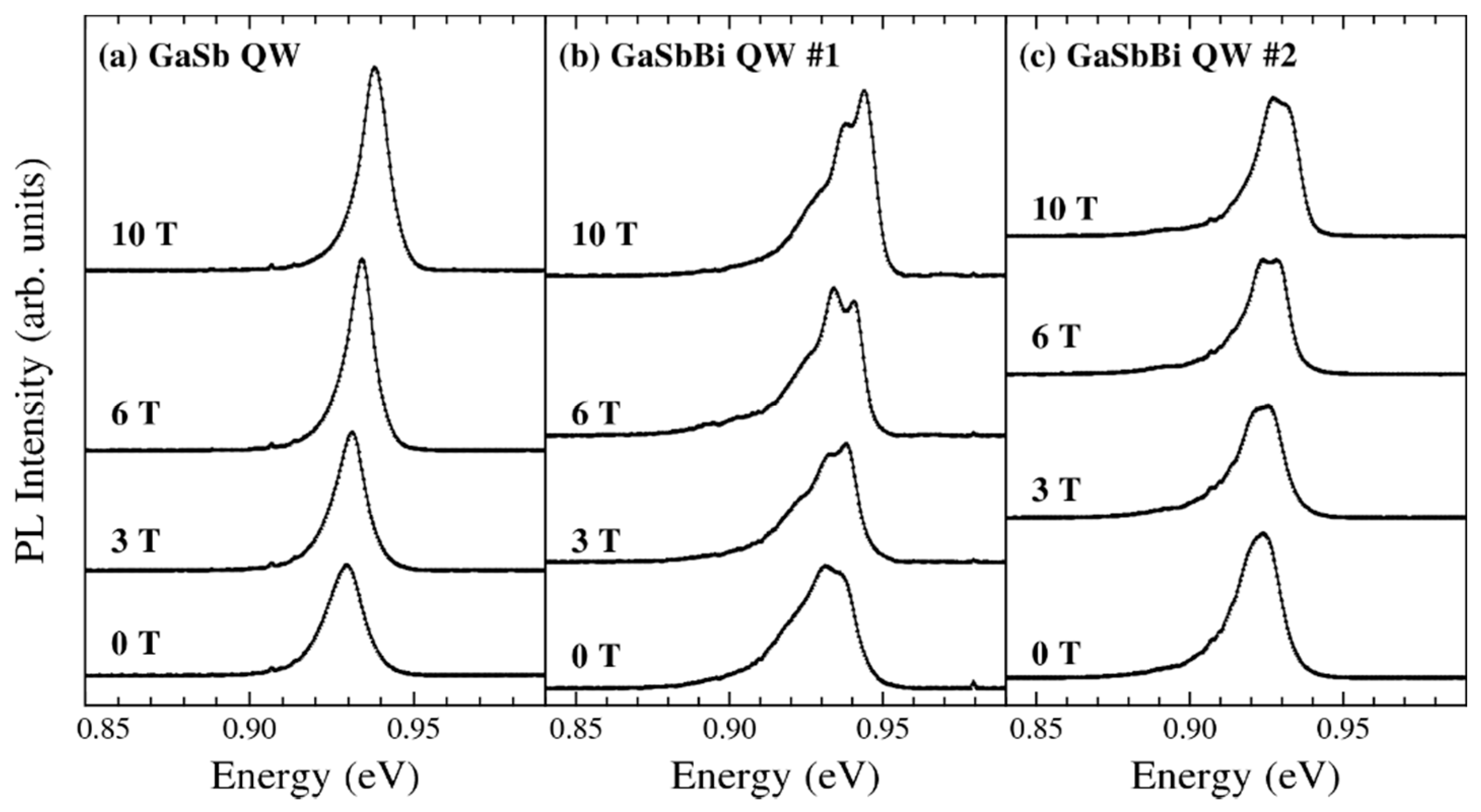
- Chen, X.; Song, Y.; Zhu, L.; Wang, S. M.; Lu, W.; Guo, S.; Shao, J. Shallow-terrace-like interface in dilute-bismuth GaSb/AlGaSb single quantum wells evidenced by photoluminescence. J. Appl. Phys. 2013, 113, 153505. [Google Scholar] [CrossRef]
- Kudrawiec, R.; Kopaczek, J.; Misiewicz, J.; Petropoulos, J.P.; Zhong, Y.; Zide, J.M.O. Contactless electroreflectance study of E0 and E0+ΔSO transitions in In0.53Ga0.47BixAs1−x alloys. Appl. Phys. Lett. 2011, 99, 251906. [Google Scholar] [CrossRef]
- Zaied, I.; Fitouri, H.; Chine, Z.; Rebey, A.; El Jani, B. Atmospheric-pressure metal-organic vapor-phase epitaxy of GaAsBi alloys on high-index GaAs substrates. J. Phys. Chem. Solids 2014, 75, 244–251. [Google Scholar] [CrossRef]
- Mazur, Y.I.; Dorogan, V.G.; Benamara, M.; Ware, M.E.; Schmidbauer, M.; Tarasov, G.G.; Johnson, S.R.; Lu, X.; Yu, S.Q.; Tiedje, T.; et al. Effects of spatial confinement and layer disorder in photoluminescence of GaAs1−xBix/GaAs heterostructures. J. Phys. D 2013, 46, 065306. [Google Scholar] [CrossRef]
- Hosea, T.J.C.; Marko, I.P.; Batool, Z.; Hild, K.; Jin, S.R.; Hossain, T.; Chai, G.M.T.; Sweeney, S.J.; Petropoulos, J.P.; Zhong, Y.; et al. InGaBiAs/InP semiconductors for mid-infrared applications: Dependence of bandgap and spin-orbit splitting on temperature and bismuth content. In Proceedings of the IEEE 3rd International Conference on Photonics, Penang, Malaysia, 1–3 October 2012; pp. 154–158.
- Song, Y.; Wang, S.; Saha Roy, I.; Shi, P.; Hallen, A.; Lai, Z. Molecular beam epitaxy growth of InSb1−xBix thin films. J. Cryst. Growth 2013, 378, 323–328. [Google Scholar] [CrossRef]
- Rajpalke, M.K.; Linhart, W.M.; Yu, K.M.; Birkett, M.; Alaria, J.; Bomphrey, J.J.; Sallis, S.; Piper, L.F.J.; Jones, T.S.; Ashwin, M.J.; et al. Bi-induced band gap reduction in epitaxial InSbBi alloys. Appl. Phys. Lett. 2014, 105, 212101. [Google Scholar] [CrossRef]
- Dixita, V.K.; Keerthia, K.S.; Berab, P.; Bhata, H.L. Growth of InBixSb1-x films on GaAs (001) substrates using liquid phase epitaxy and their characterization. J. Cryst. Growth 2002, 241, 171–176. [Google Scholar] [CrossRef]
- Ma, K.Y.; Fang, Z.M.; Cohen, R.M.; Stringfellow, G.B. OMVPE growth and characterization of Bi-containing III–V alloys. J. Cryst. Growth 1991, 107, 416–421. [Google Scholar] [CrossRef]
- Lee, J.J.; Kim, J.D.; Razeghi, M. Growth and characterization of InSbBi for long wavelength infrared photodetectors. Appl. Phys. Lett. 1997, 70, 3266. [Google Scholar] [CrossRef]
- Wagener, M.C.; Kroon, R.E.; Botha, J.R.; Leitch, A.W.R. Analysis of secondary phases in InSbBi thin flms. Phys. B-Condens. Matter 1999, 273–274, 919–922. [Google Scholar] [CrossRef]
- Du, Q.; Alperin, J.; Wang, W.I. Molecular beam epitaxial growth of GalnSbBi for infrared detector applications. J. Cryst. Growth 1997, 175/176, 849–852. [Google Scholar] [CrossRef]
- Das, S.K.; Das, T.D.; Dhar, S.; de la Mare, M.; Krier, A. Near infrared photoluminescence observed in dilute GaSbBi alloys grown by liquid phase epitaxy. Infrared Phys. Technol. 2012, 55, 156–160. [Google Scholar] [CrossRef]
- Rajpalke, M.K.; Linhart, W.M.; Birkett, M.; Yu, K.M.; Scanlon, D.O.; Buckeridge, J.; Jones, T.S.; Ashwin, M.J.; Veal, T.D. Growth and properties of GaSbBi alloys. Appl. Phys. Lett. 2013, 103, 142106. [Google Scholar] [CrossRef]
- Rajpalke, M.K.; Linhart, W.M.; Yu, K.M.; Jones, T.S.; Ashwin, M.J.; Veal, T.D. Bi flux-dependent MBE growth of GaSbBi alloys. J. Cryst. Growth 2015, 425, 241–244. [Google Scholar] [CrossRef]
- Polak, M.P.; Scharoch, P.; Kudrawiec, R.; Kopaczek, J.; Winiarski, M.J.; Linhart, W.M.; Rajpalke, M.K.; Yu, K.M.; Jones, T.S.; Ashwin, M.J. Theoretical and experimental studies of electronic band structure for GaSb1−xBix in the dilute Bi regime. J. Phys. D 2014, 47, 355107. [Google Scholar]
- Kopaczek, J.; Kudrawiec, R.; Linhart, W.M.; Rajpalke, M.K.; Yu, K.M.; Jones, T.S.; Ashwin, M.J.; Misiewicz, J.; Veal, T.D. Temperature dependence of the band gap of GaSb1−xBix alloys with 0 < x ≤ 0.042 determined by photoreflectance. Appl. Phys. Lett. 2013, 103, 261907. [Google Scholar]
- Kopaczek, J.; Kudrawiec, R.; Linhart, W.; Rajpalke, M.; Jones, T.; Ashwin, M.; Veal, T. Low- and high-energy photoluminescence from GaSb1−xBix with 0 < x ≤ 0.042. Appl. Phys. Express 2014, 7, 111202. [Google Scholar]
- Francoeur, S.; Seong, M. J.; Mascarenhas, A.; Tixier, S.; Adamcyk, M.; Tiedje, T. Band gap of GaAs1−xBix, 0 < x < 3.6%. Appl. Phys. Lett. 2003, 82, 3874. [Google Scholar]
- Wei, P.; Tixier, S.; Chicoine, M.; Francoeur, S.; Mascarenhas, A.; Tiedje, T.; Schiettekatte, F. Ion beam characterization of GaAs1−x−yNxBiy epitaxial layers. Nucl. Instrum. Methods Phys. Res. Sect. B 2004, 219–220, 671–675. [Google Scholar] [CrossRef]
- Yoshimoto, M.; Huang, W.; Takehara, Y.; Saraie, J.; Chayahara, A.; Horino, Y.; Oe, K. New semiconductor GaNAsBi alloy grown by molecular beam epitaxy. Jpn. J. Appl. Phys. 2004, 43, L845–L847. [Google Scholar] [CrossRef]
- Bushell, Z.L.; Ludewig, P.; Knaub, N.; Batool, Z.; Hild, K.; Stolz, W.; Sweeney, S.J.; Volz, K. Growth and characterisation of Ga(NAsBi) alloy by metal-organic vapour phase epitaxy. J. Cryst. Growth 2014, 396, 79–84. [Google Scholar] [CrossRef]
- Denton, A.R.; Ashcroft, N.W. Vegard’s law. Phys. Rev. A 1991, 43, 3161–3164. [Google Scholar] [CrossRef] [PubMed]
- Yoshimoto, M.; Huang, W.; Feng, G.; Oe, K. New semiconductor alloy GaNAsBi with temperature-insensitive bandgap. Phys. Status Solidi (b) 2006, 243, 1421–1425. [Google Scholar] [CrossRef]
- Beaton, D.A.; Ptak, A.J.; Alberi, K.; Mascarenhas, A. Quaternary bismide alloy lattice matched to GaAs. J. Cryst. Growth 2012, 351, 37–40. [Google Scholar] [CrossRef]
- Aslan, M.; Yalcin, B. G.; Ustundag, M.; Bagci, S. Theoretical calculations on structural and electronic properties of BGaAsBi alloys. Eur. Phys. J. B 2015, 88, 1–4. [Google Scholar] [CrossRef]
- Groenert, M.E.; Averbeck, R.; Hösler, W.; Schuster, M.; Riechert, H. Optimized growth of BGaAs by molecular beam epitaxy. J. Cryst. Growth 2004, 264, 123–127. [Google Scholar] [CrossRef]
- Hoke, W.E. Molecular-beam epitaxial growth of boron-doped GaAs films. J. Vac. Sci. Technol. B 1993, 11, 902. [Google Scholar] [CrossRef]
- Wu, X.; Chen, X.; Pan, W.; Wang, P.; Zhang, L.; Li, Y.; Wang, H.; Wang, K.; Shao, J.; Wang, S. Anomalous photoluminescence in InP1-xBix. Sci. Rep. 2016, 6, 27867. [Google Scholar] [CrossRef] [PubMed]
- Sales, D.L.; Guerrero, E.; Rodrigo, J.F.; Galindo, P.L.; Yáñez, A.; Shafi, M.; Khatab, A.; Mari, R.H.; Henini, M.; Novikov, S.; et al. Distribution of bismuth atoms in epitaxial GaAsBi. Appl. Phys. Lett. 2011, 98, 101902. [Google Scholar] [CrossRef]
- Song, Y.; Wang, S.; Saha Roy, I.; Shi, P.; Hallen, A. Growth of GaSb1−xBix by molecular beam epitaxy. J. Vac. Sci. Technol. B 2012, 30, 02B114. [Google Scholar]
- Das, T.D. The effect of Bi composition on the properties of InP1−xBix grown by liquid phase epitaxy. J. Appl. Phys. 2014, 115, 173107. [Google Scholar] [CrossRef]
- Takehara, Y.; Yoshimoto, M.; Huang, W.; Saraie, J.; Oe, K.; Chayahara, A.; Horino, Y. Lattice distortion of GaAsBi alloy grown on GaAs by molecular beam epitaxy. Jpn. J. Appl. Phys. 2006, 45, 67–69. [Google Scholar] [CrossRef]
- Kunzer, M.; Jost, W.; Kaufmann, U.; Hobgood, H.M.; Thomas, R.N. Identification of the BiGa heteroantisite defect in GaAs:Bi. Phys. Rev. B 1993, 48, 4437–4441. [Google Scholar] [CrossRef]
- Ferhat, M.; Zaoui, A. Do all III-V compounds have the zinc-blende or wurtzite ground state structure? Appl. Phys. Lett. 2006, 88, 161902. [Google Scholar] [CrossRef]
- Mascarenhas, A. Spontaneous Ordering in Semiconductor Alloys; Springer: Berlin, Germany, 2002. [Google Scholar]
- Wu, M.; Luna, E.; Puustinen, J.; Guina, M.; Trampert, A. Observation of atomic ordering of triple-period-A and -B type in GaAsBi. Appl. Phys. Lett. 2014, 105, 041602. [Google Scholar] [CrossRef]
- Reyes, D.F.; Bastiman, F.; Hunter, C.; Sales, D.L.; Sanchez, A.M.; David, J.P.R.; González, D. Bismuth incorporation and the role of ordering in GaAsBi/GaAs structures. Nanoscale Res. Lett. 2014, 9, 23. [Google Scholar] [CrossRef] [PubMed]
- Verma, P.; Oe, K.; Yamada, M.; Harima, H.; Herms, M.; Irmer, G. Raman Studies on GaAs1-xBix and InAs1-xBix. J. Appl. Phys. 2001, 89, 1657. [Google Scholar] [CrossRef]
- Janotti, A.; Wei, S.-H.; Zhang, S.B. Theoretical study of the effects of isovalent coalloying of Bi and N in GaAs. Phys. Rev. B 2002, 65, 115203. [Google Scholar] [CrossRef]
- Alberi, K.; Wu, J.; Walukiewicz, W.; Yu, K.M.; Dubon, O.D.; Watkins, S.P.; Wang, C.X.; Liu, X.; Cho, Y.J.; Furdyna, J. Valence-band anticrossing in mismatched III-V semiconductor alloys. Phys. Rev. B 2007, 75, 045203. [Google Scholar] [CrossRef]
- Pettinari, G.; Polimeni, A.; Capizzi, M.; Blokland, J.H.; Christianen, P.C.M.; Maan, J.C.; Young, E.C.; Tiedje, T. Influence of bismuth incorporation on the valence and conduction band edges of GaAs1−xBix. Appl. Phys. Lett. 2008, 92, 262105. [Google Scholar] [CrossRef]
- Pettinari, G.; Polimeni, A.; Blokland, J.H.; Trotta, R.; Christianen, P.C.M.; Capizzi, M.; Maan, J.C.; Lu, X.; Young, E.C.; Tiedje, T. Compositional dependence of the exciton reduced mass in GaAs1−xBix (x = 0%–10%). Phys. Rev. B 2010, 81, 235211. [Google Scholar] [CrossRef]
- Lu, X.; Beaton, D.A.; Lewis, R.B.; Tiedje, T.; Zhang, Y. Composition dependence of photoluminescence of GaAs1−xBix alloys. Appl. Phys. Lett. 2009, 95, 041903. [Google Scholar] [CrossRef]
- Mohmad, A.R.; Bastiman, F.; Hunter, C.J.; Richards, R.D.; Sweeney, S.J.; Ng, J.S.; David, J.P.R.; Majlis, B.Y. Localization effects and band gap of GaAsBi alloys. Phys. Status Solidi (b) 2014, 251, 1276–1281. [Google Scholar] [CrossRef]
- Kudrawiec, R.; Kopaczek, J.; Sitarek, P.; Misiewicz, J.; Henini, M.; Novikov, S.V. Unusual broadening of E0 and E0+ΔSO transitions in GaAsBi studied by electromodulation spectroscopy. J. Appl. Phys. 2012, 111, 066103. [Google Scholar] [CrossRef]
- Pettinari, G.; Patanè, A.; Polimeni, A.; Capizzi, M.; Lu, X.; Tiedje, T. Bi-induced p-type conductivity in nominally undoped Ga(AsBi). Appl. Phys. Lett. 2012, 100, 092109. [Google Scholar] [CrossRef]
- Kini, R.N.; Ptak, A.J.; Fluegel, B.; France, R.; Reedy, R.C.; Mascarenhas, A. Effect of Bi alloying on the hole transport in the dilute bismide alloy GaAs1−xBix. Phys. Rev. B 2011, 83, 075307. [Google Scholar] [CrossRef]
- Cooke, D.G.; Hegmann, F.A.; Young, E.C.; Tiedje, T. Electron mobility in dilute GaAs bismide and nitride alloys measured by time-resolved terahertz spectroscopy. Appl. Phys. Lett. 2006, 89, 122103. [Google Scholar] [CrossRef]
- Fahy, S.; Lindsay, A.; Ouerdane, H.; O’Reilly, E.P. Alloy scattering of n-type carriers in GaNxAs1−x. Phys. Rev. B 2006, 74, 035203. [Google Scholar] [CrossRef]
- Pettinari, G.; Polimeni, A.; Capizzi, M.; Engelkamp, H.; Christianen, P.C.M.; Maan, J.C.; Patanè, A.; Tiedje, T. Effects of Bi incorporation on the electronic properties of GaAs: Carrier masses, hole mobility, and Bi-induced acceptor states. Phys. Status Solidi (b) 2013, 250, 779–786. [Google Scholar] [CrossRef]
- Gelczuk, Ł.; Stokowski, H.; Kopaczek, J.; Zhang, L.; Li, Y.; Wang, K.; Wang, P.; Wang, S.; Kudrawiec, R. Bi-induced acceptor level responsible for partial compensation of native free electron density in InP1−xBix dilute bismide alloys. J. Phys. D 2016, 49, 115107. [Google Scholar] [CrossRef]
- Schäfer, W.; Wegener, M. Semiconductor Optics and Transport Phenomena; Springer: Berlin, Germany, 2013. [Google Scholar]
- Gilliland, G.D. Photoluminescence spectroscopy of crystalline semiconductors. Mater. Sci. Eng. 1997, 18, 99–440. [Google Scholar] [CrossRef]
- Shao, J.; Lu, W.; Lü, X.; Yue, F.; Li, Z.; Guo, S.; Chu, J. Erratum: “Modulated photoluminescence spectroscopy with a step-scan Fourier transform infrared spectrometer” [Review of Scientific Instruments 2006, 77, 063104]. Rev. Sci. Instrum. 2007, 78, 029901. [Google Scholar] [CrossRef]
- Shao, J.; Lu, W.; Tsen, G.K.O.; Guo, S.; Dell, J.M. Mechanisms of infrared photoluminescence in HgTe/HgCdTe superlattice. J. Appl. Phys. 2012, 112, 063512. [Google Scholar] [CrossRef]
- Shao, J.; Lü, X.; Guo, S.; Lu, W.; Chen, L.; Wei, Y.; Yang, J.; He, L.; Chu, J. Impurity levels and bandedge electronic structure in as-grown arsenic-doped HgCdTe by infrared photoreflectance spectroscopy. Phys. Rev. B 2009, 80, 155125. [Google Scholar] [CrossRef]
- Shao, J.; Lu, W.; Sadeghi, M.; Lü, X.; Wang, S.M.; Ma, L.; Larsson, A. Evolution of valence-band alignment with nitrogen content in GaNAs/GaAs single quantum wells. Appl. Phys. Lett. 2008, 93, 031904. [Google Scholar] [CrossRef]
- Chen, X.; Jung, J.; Qi, Z.; Zhu, L.; Park, S.; Zhu, L.; Yoon, E.; Shao, J. Infrared photoreflectance investigation of resonant levels and band edge structure in InSb. Opt. Lett. 2015, 40, 5295–5298. [Google Scholar] [CrossRef] [PubMed]
- Shao, J.; Chen, L.; Lü, X.; Lu, W.; He, L.; Guo, S.; Chu, J. Realization of photoreflectance spectroscopy in very-long wave infrared of up to 20 μm. Appl. Phys. Lett. 2009, 95, 041908. [Google Scholar] [CrossRef]
- Shao, J.; Lu, W.; Yue, F.; Lu, X.; Huang, W.; Li, Z.; Guo, S.; Chu, J. Photoreflectance spectroscopy with a step-scan Fourier-transform infrared spectrometer: Technique and applications. Rev. Sci. Instrum. 2007, 78, 013111. [Google Scholar] [CrossRef] [PubMed]
- Huang, K.T.; Chiu, C.T.; Cohen, R.M.; Stringfellow, G.B. InAsBi alloys grown by organometallic vapor phase epitaxy. J. Cryst. Growth 1993, 134, 29–34. [Google Scholar] [CrossRef]
- Pačebutas, V.; Bertulis, K.; Dapkus, L.; Aleksejenko, G.; Krotkus, A.; Yu, K.M.; Walukiewicz, W. Characterization of low-temperature molecular-beam-epitaxy grown GaBiAs layers. Semicond. Sci. Technol. 2007, 22, 819–823. [Google Scholar] [CrossRef]
- Chen, X.-R.; Song, Y.-X.; Zhu, L.-Q.; Qi, Z.; Zhu, L.; Zha, F.-X.; Guo, S.-L.; Wang, S.-M.; Shao, J. Bismuth effects on electronic levels in GaSb(Bi)/AlGaSb quantum wells probed by infrared photoreflectance. Chin. Phys. Lett. 2015, 32, 067301. [Google Scholar] [CrossRef]
- Kudrawiec, R.; Kopaczek, J.; Misiewicz, J.; Walukiewicz, W.; Petropoulos, J.P.; Zhong, Y.; Dongmo, P.B.; Zide, J.M.O. Temperature dependence of E0 and E0+ΔSO transitions in In0.53Ga0.47BixAs1−x alloys studied by photoreflectance. J. Appl. Phys. 2012, 112, 113508. [Google Scholar] [CrossRef]
- Pettinari, G.; Capizzi, M.; Polimeni, A. Carrier masses and band-gap temperature sensitivity in Ga(AsBi) alloys. Semicond. Sci. Technol. 2015, 30, 094002. [Google Scholar] [CrossRef]
- Fitouri, H.; Essouda, Y.; Zaied, I.; Rebey, A.; El Jani, B. Photoreflectance and photoluminescence study of localization effects in GaAsBi alloys. Opt. Mater. 2015, 42, 67–71. [Google Scholar] [CrossRef]
- Mohmad, A.R.; Bastiman, F.; Hunter, C.J.; Harun, F.; Reyes, D.F.; Sales, D.L.; Gonzalez, D.; Richards, R.D.; David, J.P.R.; Majlis, B.Y. Bismuth concentration inhomogeneity in GaAsBi bulk and quantum well structures. Semicond. Sci. Technol. 2015, 30, 094018. [Google Scholar] [CrossRef]
- Beaton, D.A.; Mascarenhas, A.; Alberi, K. Insight into epitaxy growth of high optical quality GaAs1-xBix. J. Appl. Phys. 2015, 118, 235701. [Google Scholar] [CrossRef]
- Mohmad, A.R.; Bastiman, F.; Hunter, C.J.; Ng, J.S.; Sweeney, S.J.; David, J.P.R. The effect of Bi composition to the optical quality of GaAs1−xBix. Appl. Phys. Lett. 2011, 99, 042107. [Google Scholar] [CrossRef] [Green Version]
- Gu, Y.; Zhang, Y.G.; Chen, X.Y.; Xi, S.P.; Du, B.; Ma, Y.J. Effect of bismuth surfactant on InP-based highly strained InAs/InGaAs triangular quantum wells. Appl. Phys. Lett. 2015, 107, 212104. [Google Scholar] [CrossRef]
- Oe, K. Characteristics of semiconductor alloy GaAs1-xBix. Jpn. J. Appl. Phys. 2002, 41, 2801–2806. [Google Scholar] [CrossRef]
- Imhof, S.; Thränhardt, A.; Chernikov, A.; Koch, M.; Köster, N.S.; Kolata, K.; Chatterjee, S.; Koch, S.W.; Lu, X.; Johnson, S.R.; et al. Clustering effects in Ga(AsBi). Appl. Phys. Lett. 2010, 96, 131115. [Google Scholar] [CrossRef]
- Shakfa, M.K.; Wiemer, M.; Ludewig, P.; Jandieri, K.; Volz, K.; Stolz, W.; Baranovskii, S.D.; Koch, M. Thermal quenching of photoluminescence in Ga(AsBi). J. Appl. Phys. 2015, 117, 025709. [Google Scholar] [CrossRef]
- Seonga, M.J.; Francoeura, S.; Yoon, S.; Mascarenhasa, A.; Tixierb, S.; Adamcyk, M.; Tiedje, T. Bi-induced vibrational modes in GaAsBi. Superlattices Microstructures 2005, 37, 394–400. [Google Scholar] [CrossRef]
- Marko, I.P.; Jin, S.R.; Hild, K.; Batool, Z.; Bushell, Z.L.; Ludewig, P.; Stolz, W.; Volz, K.; Butkutė, R.; Pačebutas, V.; et al. Properties of hybrid MOVPE/MBE grown GaAsBi/GaAs based near-infrared emitting quantum well lasers. Semicond. Sci. Technol. 2015, 30, 094008. [Google Scholar] [CrossRef]
- Lewis, R.B.; Beaton, D.A.; Lu, X.; Tiedje, T. GaAs1-xBix light emitting diodes. J. Cryst. Growth 2009, 311, 1872–1875. [Google Scholar] [CrossRef]
- Zvonkov, B.N.; Karpovich, I.A.; Baidus, N.V.; Filatov, D.O.; Morozov, S.V.; Gushina, Y.Y. Surfactant effect of bismuth in the MOVPE growth of the InAs quantum dots on GaAs. Nanotechnology 2000, 11, 221–226. [Google Scholar] [CrossRef]
- Reyes, D.F.; González, D.; Bastiman, F.; Dominguez, L.; Hunter, C.J.; Guerrero, E.; Roldan, M.A.; Mayoral, A.; David, J.P.R.; Sales, D.L. Photoluminescence enhancement of InAs(Bi) quantum dots by Bi clustering. Appl. Phys. Express 2013, 6, 042103. [Google Scholar] [CrossRef]
- Dasika, V.D.; Krivoy, E.M.; Nair, H.P.; Maddox, S.J.; Park, K.W.; Jung, D.; Lee, M.L.; Yu, E.T.; Bank, S.R. Increased InAs quantum dot size and density using bismuth as a surfactant. Appl. Phys. Lett. 2014, 105, 253104. [Google Scholar] [CrossRef]
- Essouda, Y.; Fitouri, H.; Boussaha, R.; Elayech, N.; Rebey, A.; Jani, B.E. Bismuth catalyzed growth of GaAsBi nanowires by metalorganic vapor phase epitaxy. Mater. Lett. 2015, 152, 298–301. [Google Scholar] [CrossRef]
- Shimomura, K.; Kamiya, I. Strain engineering of quantum dots for long wavelength emission: Photoluminescence from self-assembled InAs quantum dots grown on GaAs(001) at wavelengths over 1.55 μm. Appl. Phys. Lett. 2015, 106, 082103. [Google Scholar] [CrossRef]
- Bimberg, D. Quantum dots for lasers, amplifiers and computing. J. Phys. D 2005, 38, 2055–2058. [Google Scholar] [CrossRef]
- Copel, M.; Reuter, M.C.; Kaxiras, E.; Tromp, R.M. Surfactants in epitaxial growth. Phys. Rev. Lett. 1989, 63, 632–635. [Google Scholar] [CrossRef] [PubMed]
- Lyman, P.F.; Bedzyk, M.J. Surfactant-mediated epitaxy of metastable SnGe alloys. Appl. Phys. Lett. 1996, 69, 978–980. [Google Scholar] [CrossRef]
- Ciatto, G.; Young, E.C.; Glas, F.; Chen, J.; Mori, R.A.; Tiedje, T. Spatial correlation between Bi atoms in dilute GaAs1−xBix: From random distribution to Bi pairing and clustering. Phys. Rev. B 2008, 78, 035325. [Google Scholar] [CrossRef]
- Sweeney, S.J.; Adams, A.R.; Silver, M.; O’Reilly, E.P.; Watling, J.R.; Walker, A.B.; Thijs, P.J.A. Dependence of threshold current on QW position and on pressure in 1.5 μm InGaAs(P) lasers. Phys. Status Solidi (b) 1999, 211, 525–531. [Google Scholar] [CrossRef]
- Hunter, C.J.; Bastiman, F.; Mohmad, A.R.; Richards, R.; Ng, J.S.; Sweeney, S.J.; David, J.P. Absorption characteristics of diodes in the near-infrared. IEEE Photonics Technol. Lett. 2012, 24, 2191–2194. [Google Scholar] [CrossRef]
- Tominaga, Y.; Oe, K.; Yoshimoto, M. Low temperature dependence of oscillation wavelength in GaAs1-xBix laser by photo-pumping. Appl. Phys. Express 2010, 3, 062201. [Google Scholar] [CrossRef]
- Fuyuki, T.; Yoshioka, R.; Yoshida, K.; Yoshimoto, M. Long-wavelength emission in photo-pumped GaAs1−xBix laser with low temperature dependence of lasing wavelength. Appl. Phys. Lett. 2013, 103, 202105. [Google Scholar] [CrossRef]
- Fuyuki, T.; Yoshida, K.; Yoshioka, R.; Yoshimoto, M. Electrically pumped room-temperature operation of GaAs1−xBix laser diodes with low-temperature dependence of oscillation wavelength. Appl. Phys. Express 2014, 7, 082101. [Google Scholar] [CrossRef]
- Marko, I. P.; Ludewig, P.; Bushell, Z. L.; Jin, S. R.; Hild, K.; Batool, Z.; Reinhard, S.; Nattermann, L.; Stolz, W.; Volz, K.; Sweeney, S.J. Physical properties and optimization of GaBiAs/(Al)GaAs based near-infrared laser diodes grown by MOVPE with up to 4.4% Bi. J. Phys. D 2014, 47, 345103. [Google Scholar] [CrossRef]
- Kim, H.; Forghani, K.; Guan, Y.; Luo, G.; Anand, A.; Morgan, D.; Kuech, T.F.; Mawst, L.J.; Lingley, Z.R.; Foran, B.J.; et al. Strain-compensated GaAs1−yPy/GaAs1−zBiz/GaAs1−yPy quantum wells for laser applications. Semicond. Sci. Technol. 2015, 30, 094011. [Google Scholar] [CrossRef]
- Sandall, I.C.; White, B.; Richards, R.; Mendes, D.; David, J.P.R.; Tan, C.H. Demonstration of InAsBi photoresponse beyond 3.5 μm. Appl. Phys. Lett. 2014, 104, 171109. [Google Scholar] [CrossRef]
- Gu, Y.; Zhang, Y.G.; Chen, X.Y.; Ma, Y.J.; Xi, S.P.; Du, B.; Li, H. Nearly lattice-matched short-wave infrared InGaAsBi detectors on InP. Appl. Phys. Lett. 2016, 108, 032102. [Google Scholar] [CrossRef]
- Arlauskas, A.; Svidovsky, P.; Bertulis, K.; Adomavičius, R.; Krotkus, A. GaAsBi photoconductive terahertz detector sensitivity at long excitation wavelengths. Appl. Phys. Express 2012, 5, 022601. [Google Scholar] [CrossRef]
- Pačebutas, V.; Urbanowicz, A.; Cicėnas, P.; Stanionytė, S.; Bičiūnas, A.; Nevinskas, I.; Krotkus, A. Growth and characterization of quaternary (GaIn)(AsBi) layers for optoelectronic terahertz detector applications. Semicond. Sci. Technol. 2015, 30, 094012. [Google Scholar] [CrossRef]
- Thomas, T.; Mellor, A.; Hylton, N.P.; Führer, M.; Alonso-Álvarez, D.; Braun, A.; Ekins-Daukes, N.J.; David, J.P.R.; Sweeney, S.J. Requirements for a GaAsBi 1 eV sub-cell in a GaAs-based multi-junction solar cell. Semicond. Sci. Technol. 2015, 30, 094010. [Google Scholar] [CrossRef]
- Dongmo, P.; Zhong, Y.; Attia, P.; Bomberger, C.; Cheaito, R.; Ihlefeld, J.F.; Hopkins, P.E.; Zide, J. Enhanced room temperature electronic and thermoelectric properties of the dilute bismuthide InGaBiAs. J. Appl. Phys. 2012, 112, 093710. [Google Scholar] [CrossRef]


| Method | Electronic Properties | Optical Properties |
|---|---|---|
| BAC/VBAC Model | GaAs1−xBix [58,59,60] | GaAs1−xBix [58,59] |
| GaAsBiN= | ||
| GaAsBiN [53] | InGaAs1−xBix [61,62] | |
| GaBixAs1−x/GaAs [63] | In0.53Ga0.47BixAs1−x/InP [64] | |
| InP1−xBix [65] | ||
| InSb1−xBix [66] | ||
| InGaAs1−xBix [61,62] | ||
| In0.53Ga0.47BixAs1−x/InP [64] | ||
| TB Model | GaP1-xBix, GaAs1-xBix [67] | GaAs1−xBix [67] |
| GaAs1−xBix [68,69] | ||
| k·p Model | GaAs1−xBix [58,70] | |
| GaBixAs1−x/GaAs [63] | ||
| InGaNAs [71] | ||
| InGaAs1−xBix [72] |
| Structure | Structural Properties | Electronic Properties | Optical Properties |
|---|---|---|---|
| Thin Film | BBi/GaBi/AlBi [75,76,92] AlN1−xBix [81] GaN1−xBix [82] GaAs1−xBix [77,78,86,93,96] | BBi/GaBi/AlBi [75,76,92] AlN1–xBix [81] GaN1–xBix [82] GaAs1-xBix [60,68,69,77,78,79,86,93,96,97] InP1–xBix [73,83] InSb1–xBix [74,80] | GaAs1−xBix [93,96,97] |
| Surface | Bi/GaAs(001)-c(4 × 4)surface [85] Bi/GaAs(100) (2 × 1) and (2 × 4) surfaces [84] | ||
| Nanostructure | Bi-doped GaAs NWs [94] Bi4+ ions [98] Bi-NWs, Nanotubes [87] Bicluster [88,89,90,91] | Bi doped GaAs NWs [94] Bi4+ ions [98] Bi NWs, Nanotubes [87] Bi cluster [88,89,90,91] | Bi-doped GaAs NWs [94] |
| Stable Phase | a (Å) | c (Å) | Eg (eV) | Band Type | |
|---|---|---|---|---|---|
| BBi | ZB [102] | 5.390 ~ 5.529 [102] | — | −0.085 (FP-LAPW) [102] | I [103] |
| — | 1.134 (PW-PP) [103] | ||||
| AlBi | ZB [102] | 6.266 ~ 6.460 [102] | — | −1.81 (FP-LAPW) [102] | D [103] |
| — | 0.042 (PW-PP) [103] | ||||
| — | 0.02 (FP-LAPW) [92] | ||||
| GaBi | ZB [102] | 6.178 ~ 6.470 [102] | — | −2.91 (FP-LAPW) [102] | C [103] |
| — | 0 (PW-PP) [103] | ||||
| InBi | PbO [102] | 5.000 [102] | 4.800 [102] | −4.75 (FP-LAPW) [102] | C [103] |
| 0 (PW-PP) [103] |
| Lu | Lewis | Ptak | |
|---|---|---|---|
| Growth Temperature | 300 °C | 330 °C | 315 °C |
| As flux | 2.2 nm−2·s−1 | As2:Ga = 0.5–0.68 | As:Ga = 1.4 |
| Growth rate | - | 1 µm/h | 0.16–2.0 µm/h |
| Bi flux | Bi:As = 0.01–7 4 × 10⁻⁹ − 2.8 × 10⁻⁷ Torr | Bi:Ga BEPR = 0–0.3 (0–1.2) × 10−7 Torr | (0–3.3) × 10−8 Torr |
| Reference | Material | xBi | Epitaxy | Growth Temp (°C) | RTA Temp (°C) | RTA Time (s) | PL (λ) | PL Intensity |
|---|---|---|---|---|---|---|---|---|
| [143] | GaAsBi (QW) | 0.6%–10.9% | MBE | 345–400 | 500–900 | 600 | No shift up to 700 °C | - |
| [144] | GaAsBi (bulk) | 3.5%–6% | MBE | 220–330 | 550–750 | 30–180 | Almost no shift | 3× |
| [145] | GaAsBi (QW) | 2.2%–6.5% | MBE | 380–420 | 600–800 | 30 | No shift up to 800 °C | 3× for xBi = 4% |
| 2× for xBi = 6.5% | ||||||||
| [141] | GaAsBi (bulk) | 1.29%–1.46% | MBE | 220–315 | 500–800 | 30 | - | - |
| [146] | GaAsBi (bulk) | 2.3% | MBE | 200–350 | 750 | No shift | 1.3× | |
| [147] | GaAsBi (QW) | 3%–5.5% | MBE | - | 450–750 | - | No shift in PL | 2.2× |
| 60 meV red shift in PR | ||||||||
| [148] | GaAsBi (bulk) | 3.7% | MOVPE | 420 | 500–750 | 60 | No shift | 10×@10 K |
| [149] | GaAsBi (bulk) | 3.5% | MOVPE | 420 | 550–700 | 900 | No shift in PL | - |
| 60 meV red shift in PR | ||||||||
| [150] | GaAsNBi (bulk) | 3.2% | MBE | 365 | 800 | 900 | 8 meV @GaAsBi | 1×@GaAsBi |
| 1.4%@N | MBE | 60 | 27.5 meV @GaAsNBi | >10×@GaAsNBi | ||||
| [151] | InGaAsBi (QW) | 1% | MBE | 370–440 | 650–750 | 120 | 65 meV | 3× |
| [152] | InPBi (bulk) | 0.1–2.6% | MBE | 325 | 400–800 | 120 | No shift up to 600 °C | 1× |
| Alloy | GaBi | InBi |
|---|---|---|
| 6.23 Å [204] | 6.5 Å [158] | |
| 6.272 Å [167] | 6.686 Å [203] | |
| 6.33 Å [141] | 7.024 Å [26] |
| Ref. | Epitaxy Method | Growth Condition | Bi Influence | PL |
|---|---|---|---|---|
| [251] | MOCVD | 5 ML InAs @ 510–530 °C, Bi = 0.01–0.1 ML | Surfactant effect LD↓ | 0.93 eV @ 77 K 1.46 µm @ 300 K |
| [114] | MOCVD | InAs/InGaAs DWELL @400 °C calibrated Tg | Surfactant effect LD↑ | IPL & λ improved |
| [112] | MBE | 2.5 ML@480 °C Bi = 8 × 10⁻⁸ Torr | Surfactant effect LD↑ | IPL improved |
| [252] | MBE | 2.2 ML@400 °C Bi = 0.015–0.06 ML/s | Surfactant effect, Incorporation effect | IPL & λ improved |
| [253] | MBE | 2.3-3.3 ML@500 °C Bi = 5 × 10⁻⁸ Torr | Surfactant effect LD ↓ | IPL, FWHM & λ improved |
© 2017 by the authors. Licensee MDPI, Basel, Switzerland. This article is an open access article distributed under the terms and conditions of the Creative Commons Attribution (CC BY) license ( http://creativecommons.org/licenses/by/4.0/).
Share and Cite
Wang, L.; Zhang, L.; Yue, L.; Liang, D.; Chen, X.; Li, Y.; Lu, P.; Shao, J.; Wang, S. Novel Dilute Bismide, Epitaxy, Physical Properties and Device Application. Crystals 2017, 7, 63. https://doi.org/10.3390/cryst7030063
Wang L, Zhang L, Yue L, Liang D, Chen X, Li Y, Lu P, Shao J, Wang S. Novel Dilute Bismide, Epitaxy, Physical Properties and Device Application. Crystals. 2017; 7(3):63. https://doi.org/10.3390/cryst7030063
Chicago/Turabian StyleWang, Lijuan, Liyao Zhang, Li Yue, Dan Liang, Xiren Chen, Yaoyao Li, Pengfei Lu, Jun Shao, and Shumin Wang. 2017. "Novel Dilute Bismide, Epitaxy, Physical Properties and Device Application" Crystals 7, no. 3: 63. https://doi.org/10.3390/cryst7030063