Article

A 130 GHz Electro-Optic Ring Modulator with Double-Layer Graphene

Key Laboratory for Wide Band Gap Semiconductor Materials and Devices of Education, School of Microelectronics, Xidian University, Xi’an 710071, China
*
Authors to whom correspondence should be addressed.
Crystals 2017, 7(3), 65; https://doi.org/10.3390/cryst7030065
Submission received: 1 January 2017 / Revised: 14 February 2017 / Accepted: 23 February 2017 / Published: 26 February 2017

Abstract

:
The optical absorption coefficient of graphene will change after injecting carriers. Based on this principle, a high-speed double-layer graphene electro-optic modulator with a ring resonator structure was designed in this paper. From the numerical simulations, we designed a modulator. Its optical bandwidth is larger than 130 GHz, the switching energy is 0.358 fJ per bit, and the driven voltage is less than 1.2 V. At the same time, the footprint of the proposed modulator is less than 10 microns squared, which makes the process compatible with the Complementary Metal Oxide Semiconductors (CMOS) process. This will provide the possibility for the on-chip integration of the photoelectric device.

Graphical Abstract

1. Introduction

Optical modulators are key components for telecommunications and optical interconnections. Researchers have paid a lot of attention and effort to reducing their dimensions and integrating them onto silicon substrates [1].
Traditional straight waveguide modulators work due to the plasma dispersion effect: the optical absorption coefficient of silicon losses are modified upon the injection of free carriers [2,3,4]. However, due to the weak light-silicon interaction, an interaction length in the range of millimeters is needed. As for the Mach-Zehnder modulator [5,6,7], the refractive index of the material is modified through Kramers-Kronig relations. It is used to produce a π-shift in one of the Mach-Zehnder arms, and then the desired intensity modulation is obtained by optical interference. As this effect induces small variations of the refractive index, this device still has relatively large dimensions.
The plasma dispersion effect is still the key physical mechanism of ring resonator modulators [8,9,10,11]. However, the light will travel thousands of loops in the ring waveguide; in this way, even a tiny variation of the refractive index may lead to a huge shift of the resonant wavelength, and the intensity of emergent light is modulated. Based on this idea, this kind of device can be made in a small size, but the tradeoff is the limited bandwidth of a few GHz that the resonances can offer.
Recently, graphene has attracted great interest for its high electron mobility and broad bandwidth ranges of optical absorption. Many papers about graphene on photonic integrated circuits, especially about waveguide integrated graphene modulators and photodetectors have been published in the last few years [12,13,14]. The first graphene-based modulator was manufactured by Liu. M’s group in 2011 [15]. Unfortunately, the optical absorption loss of monolayer graphene is just 0.1 dB/μm. This means that a 30 μm interaction length is needed, if we are looking for a 3 dB modulation depth. Many different kinds of graphene modulators were proposed [16,17,18,19,20], including the ring resonator modulators with graphene on top of them [21,22,23]. These kinds of electro-optic modulators have both broad bandwidth and small dimensions at the same time.
In this paper, we have studied this type of graphene-embedded ring resonator modulator. By optimizing the design, the modulator performs better than most of the other graphene-integrated waveguide modulators proposed presently in terms of bandwidth, modulation speed, switching energy, etc.

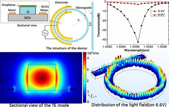
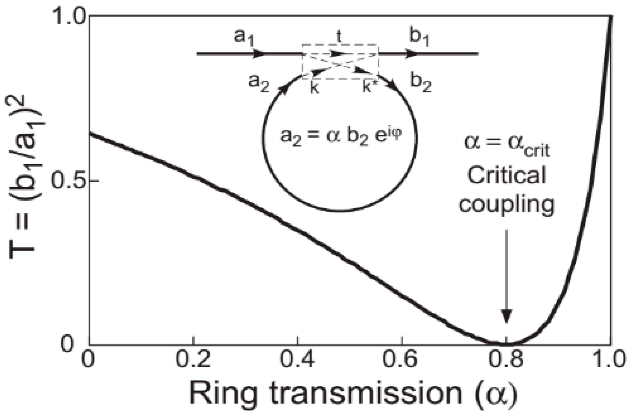
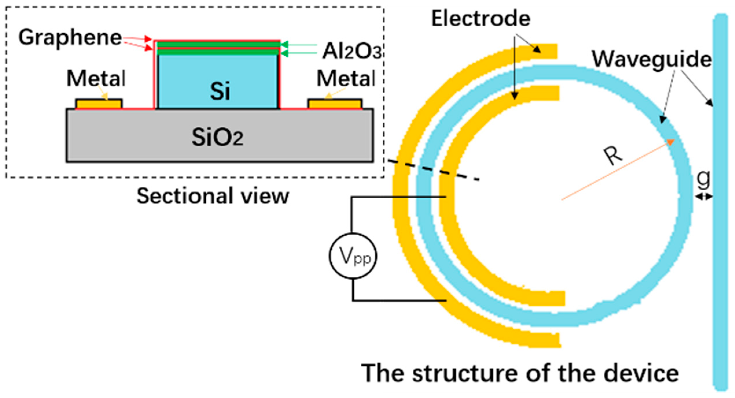
2. Principle of Operation

The physical effect of the ring resonator is exploited as follows: the critical coupling that is obtained in the ring structure is sketched in the inset of Figure 1 [23,24].
Introduced in 2002 by A. Yariv, and for the sake of clarity, we briefly review the main result of reference [24], and we use the same symbols as in the original paper; t and α as the single–pass transmission through the straight waveguide, and through the ring, respectively. At resonance (φ = m2π), the transmitted power is
T = | b 1 a 1 | 2 = ( α | t | 2 ) ( 1 α | t | 2 )
When α ≡ αcrit = t, no power is transmitted; whereas, when α→1, almost unitary transmission is obtained (at the wavelength of the resonance). The rapid control of α is precisely what one can obtain with graphene, and this is the operation principle that we want to investigate.
The device grown on the SiO2 substrate (relative index of 1.444) is shown in Figure 2. The radius of the ring R is 1.2 μm. The gap between the straight waveguide and the ring waveguide g is 80 nm. The width and height of the waveguide are 400 nm and 340 nm, respectively. The graphene-on-graphene structure is placed on the top of the silicon waveguide (relative index of 3.477). The average length of graphene L is 3.5 μm. They are separated by a thin layer of 10 nm Al2O3 (relative index of 1.765). This two-layer graphene is connected to the Pd electrodes with a width of 100 nm. We assume that the electrodes are far away from the silicon waveguide, so that they will not influence the optical mode.

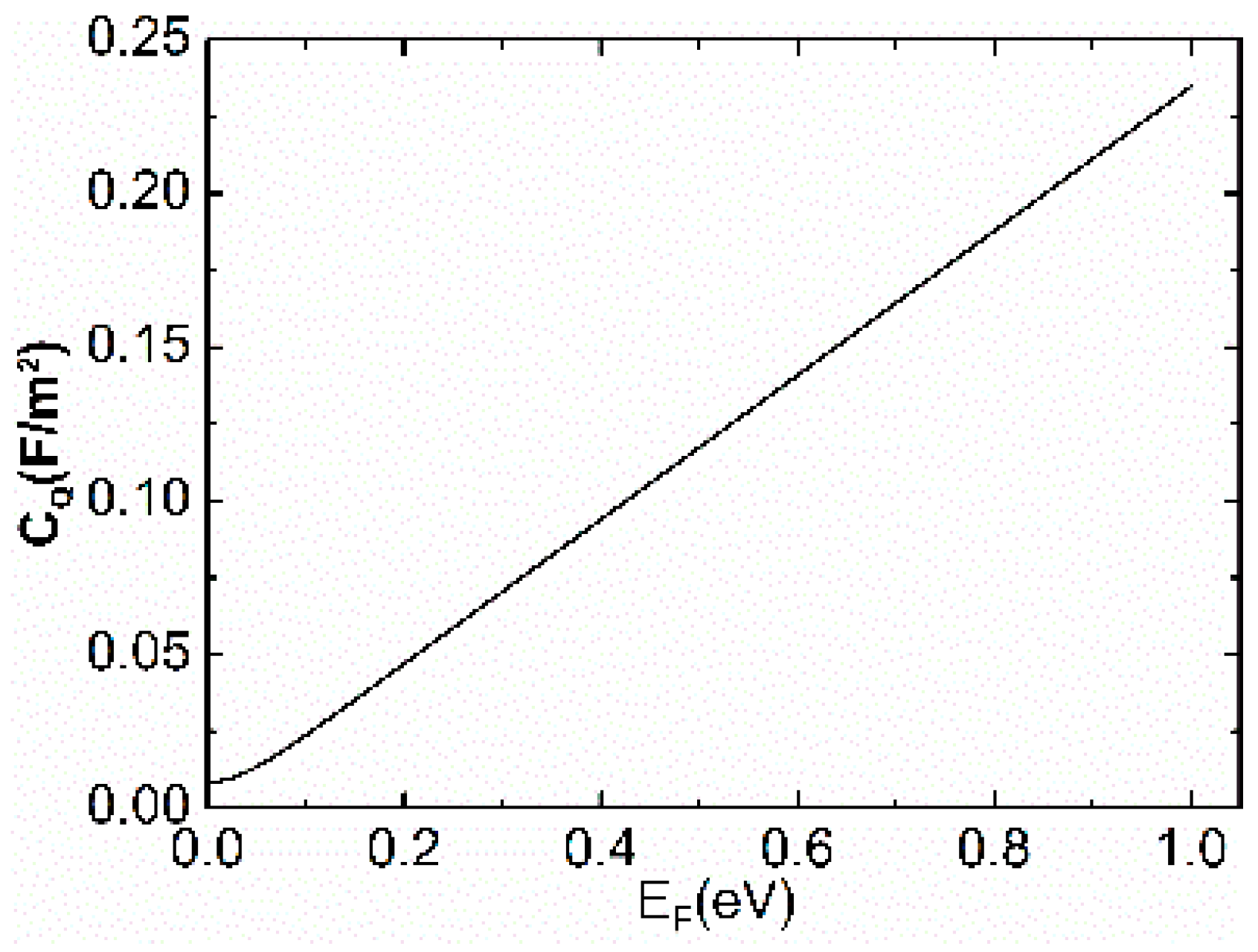
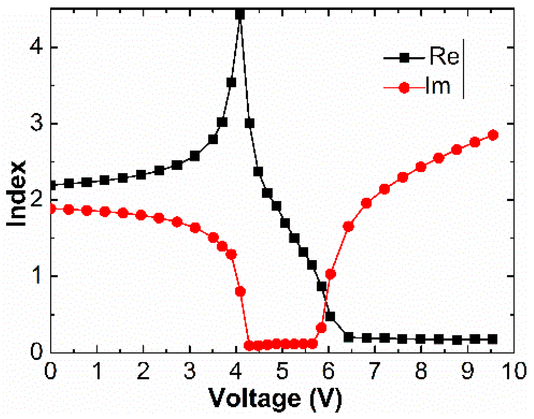
3. Relative Index of Graphene

By simplified the graphene-on-graphene structure as a plate capacitance model [19], the carrier densities of graphene can be changed by applying a voltage V as
n S = ε 0 ε r e d ( V + V 0 )
where V0 is the offset voltage caused by doping, ε0 is the dielectric constant of the vacuum, εr is the relative permittivity of the medium, e is the electron charge, and d is the thickness of Al2O3 between the two-layer graphene.
The Fermi level of graphene [19] is extracted by
E F = ν F π n S
where νF is the Fermi velocity.
The graphene conductivity σ obtained by the Kubo formula including the inter-band transition and intra-band transition is
σ t o t a l = σ int r a + σ int e r + σ int e r
where σtotal is the total optical conductivity of graphene, consisting of inter-band σ′inter, σ″inter, and intra-band σintra contributions as
σ int ra = σ 0 4 E F π ( τ 1 i ω )
σ int e r = σ 0 ( 1 + 1 π arctan ω 2 E F τ 2 1 π arctan ω + 2 E F τ 2 )
σ int e r = σ 0 1 2 π ln ( 2 E F + ω ) 2 + ( τ 2 ) 2 ( 2 E F ω ) 2 + ( τ 2 ) 2
where the universal optical conductance σ0 is 60.8 μS, the angular frequency ω is 0.8 eV (corresponding to 1550 nm), T = 296 K, the inter-band conductivity τ1 is 1.2 ps, and the intra-band conductivity τ2 is 10 fs. The conductivity of graphene is calculated as a function of the Fermi level EF, by using
n = ε = 1 + i σ t o t a l ω ε 0 d g
where the graphene layer thickness dg is 0.7 nm, and the relative index of graphene is acquired.
As shown in Figure 3, the graphene transforms to a metal from a dielectric [25] at around 6 V. The transform voltage can be below 1.5 V by doping the graphene, and the range of modulation voltage can be less than 1.2 V.

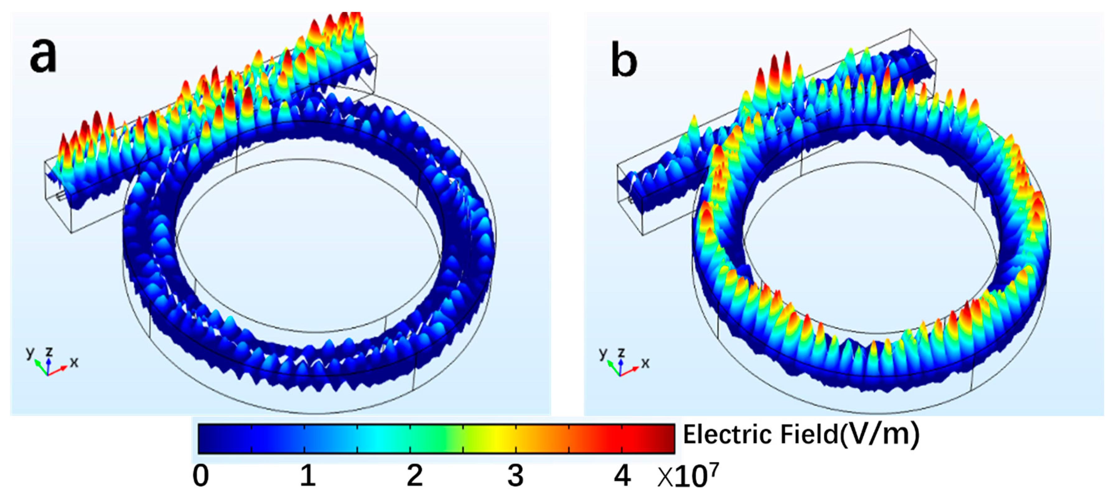
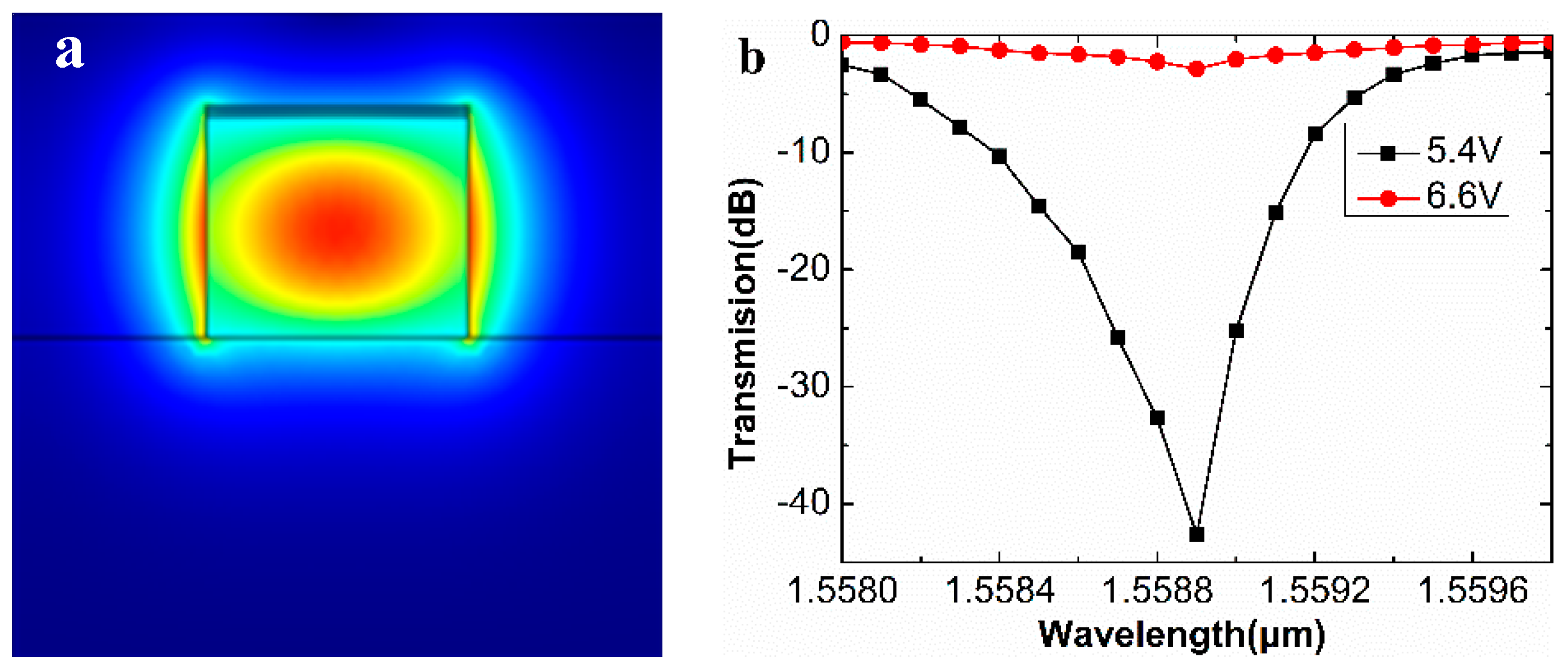
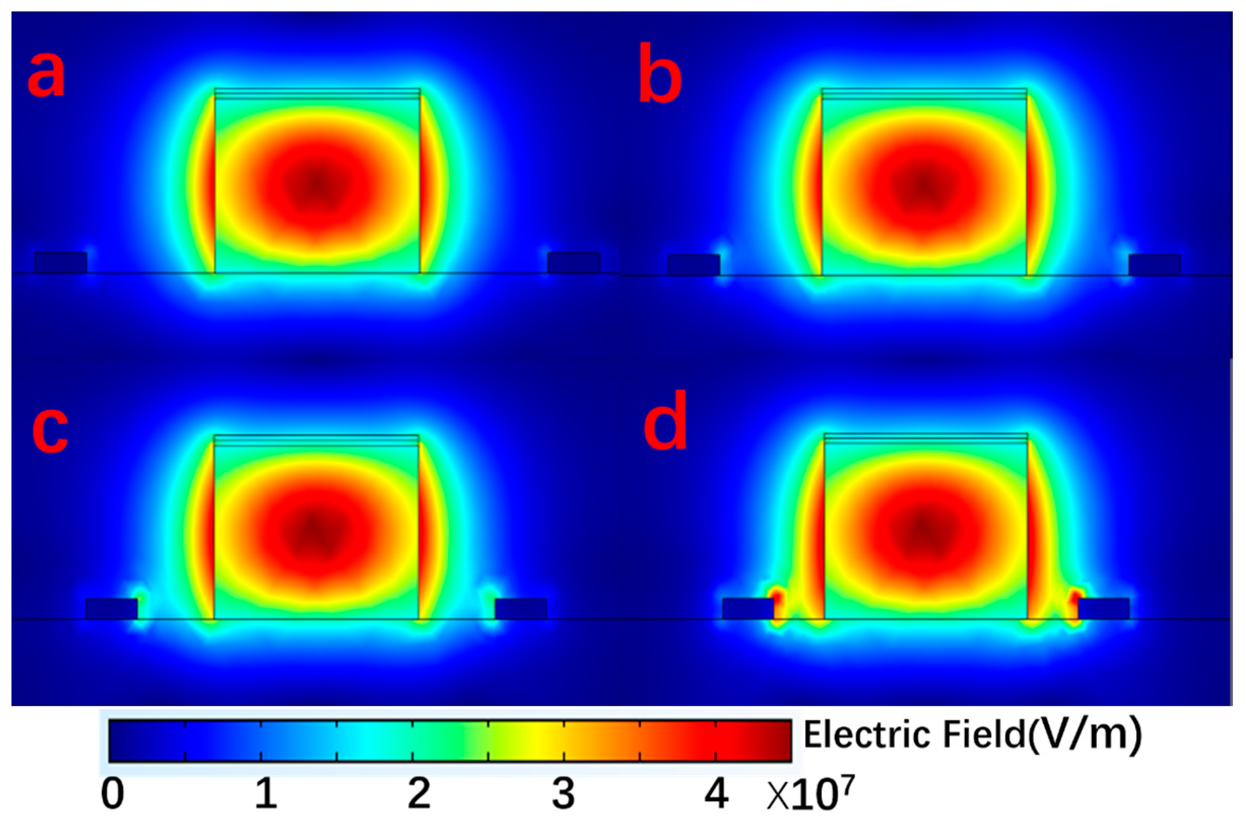
4. Numerical Simulations and Optimization

All the simulations were performed with commercial code COMSOL. Frequency-domain simulations based on the finite-element method were performed with the code. Using two-dimensional mode analysis, the optical travel mode in the waveguide was obtained, as shown in Figure 4a. Both statuses of the metallic graphene and the dielectric graphene were analyzed. For the free space-wavelength λ = 1550 nm, the mode has following effective index:
  • With dielectric graphene (ng = 1.332 + i0.105, voltage = 5.4 V) neff = 2.2755 − i6.2283 × 10−5
  • With metallic graphene (ng = 0.174 + i1.672, voltage = 6.6 V) neff = 2.2756 − i4.3248 × 10−3
It shows that graphene has little effect on the real part of the waveguide’s effective index, but has a larger influence on the imaginary part, which means that the waveforms and locations of the transmission curves are similar, but the losses are different.
Figure 4b shows the transmission curve as a function of the wavelength. The critical coupling wavelength is about 1.5598 μm. When the modulation voltage is 5.4 V, the device works in the “ON” state with an insertion loss less than 3 dB. At 6.6 V, the device works in the “OFF” state, with a largest modulation depth about 40 dB. It is observed that the 3 dB optical bandwidth is larger than 130 GHz.
Figure 5a shows the “ON” state light field diagrams of the device. Light transmits through the bus waveguide with low losses. Figure 5b shows the “OFF” state light field diagrams. Light couples into the ring waveguide, and there is nearly no light exit from the outer port.
As the radius of the ring R is 1.2 μm, the electrode inside the ring may not be very far away from the silicon waveguide. Hence, we changed the gap between the electrodes and the waveguide to see whether the electrodes will influence the optical mode or not. The distribution of the electric field in Figure 6 provides that the electrodes hardly influence the optical mode as long as the gap is greater than 200 nm. It is far smaller than the radius of the ring.
Figure 7 shows the process of optimizing our design through changing the design parameters of R, L, and g. Balancing the 3 dB bandwidth, the energy consumption, and modulation depth, we obtained the appropriate parameters of R, L, and g to be 1.2 μm, 3.5 μm, and 80 nm, respectively.

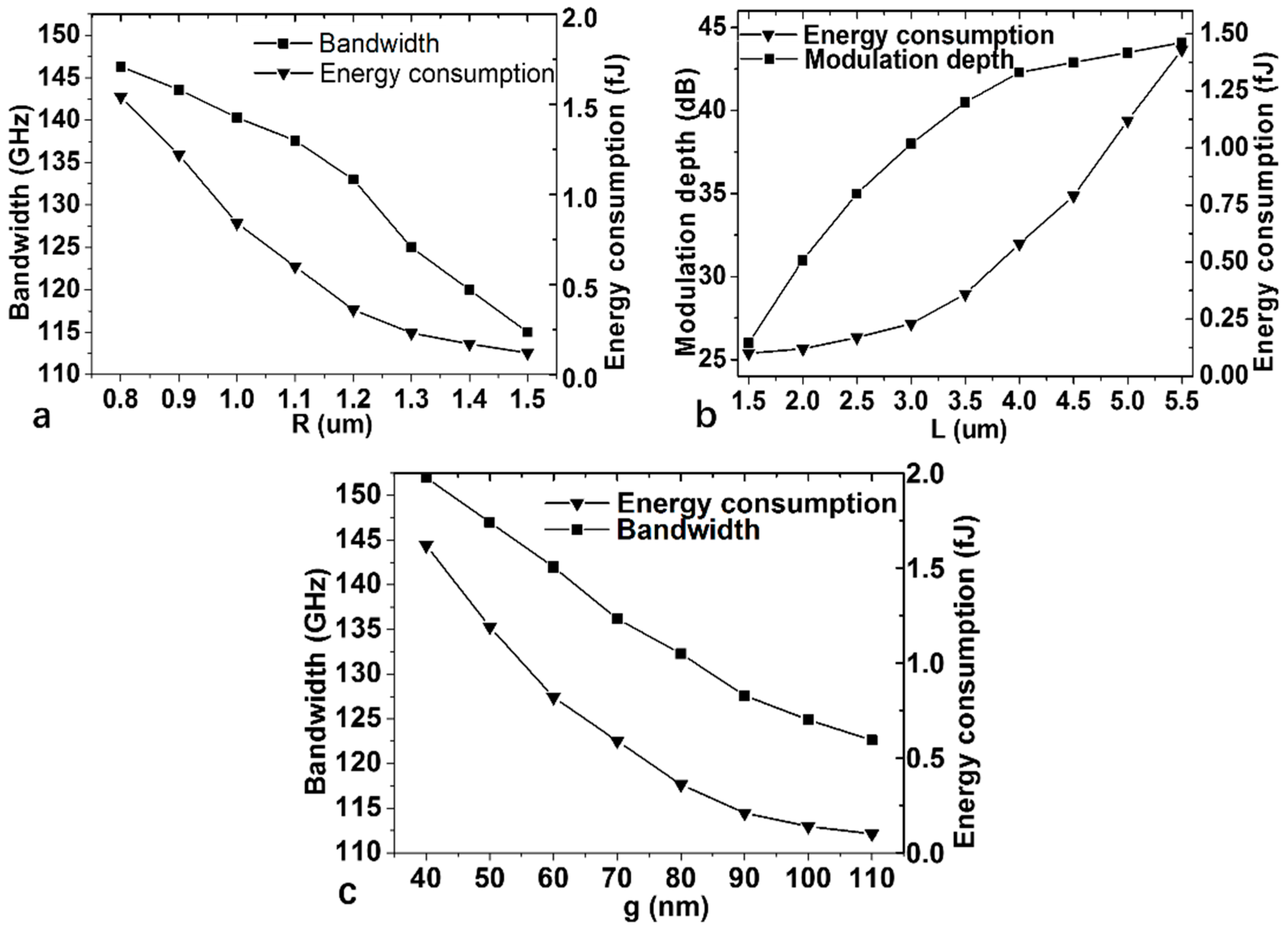
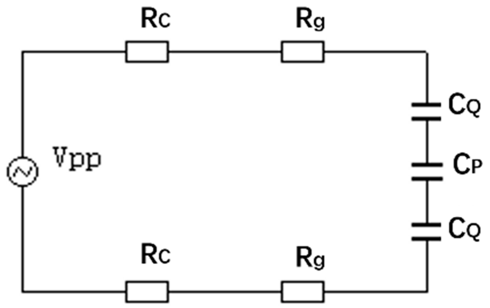
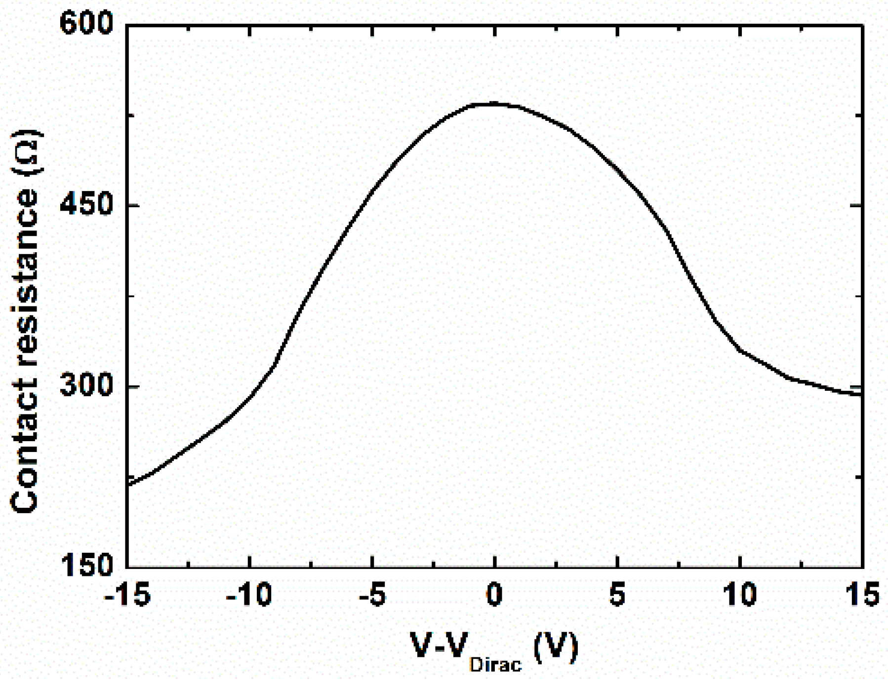
5. Estimation of Modulation Speed and Energy Required

Based on the device structure and the assumptions determined above, we can utilize the equivalent circuit shown in Figure 8 to calculate the modulation speed as:
f = 1 2 π R C
where R and C are the resistance and the capacitance of the modulator, respectively. R is composed of Rc (the resistance between the metal and graphene layer) and Rg (the resistance of graphene in series). C is composed of the quantum capacitance in either graphene sheet CQ and the oxide capacitance Cp in series.
First, we analyzed the capacitance. The equivalent capacitance C could be calculated as follows
C = 0.5 C Q C p 0.5 C Q + C p
For a typical material system, such as a metal or semiconductor, the quantum density of the system is large enough that a limited charge build-up does not produce a significant shift in the Fermi level. In this situation, its quantum capacitance is equivalent to infinity. As for graphene, due to its nanometer scale size, its electron motions are subjected to quantum confinement, leading to a low state density [26]. In this case, in order to inject enough charge into the graphene, we need to make the Fermi level move significantly. The densities of the electrons and holes in the graphene are
n = 2 π ( k T ν F ) 2 ξ 1 ( + η ) ,   and   p = 2 π ( k T ν F ) 2 ξ 1 ( η )
where
ξ j ( η i ) = 1 Γ ( j + 1 ) 0 u j 1 + e u η d u ,   and   η = E F k T
Equation (11) is the Fermi-Dirac integral, k is the Boltzmann constant, is the reduced Planck constant, Γ is the gamma function, and EF is the Fermi level of graphene. According to the definition of quantum capacitance:
C Q = e ρ E F
We obtain the quantum capacitance as a function of the Fermi level by joining solutions (11)–(13):
C Q = 2 e 2 k T π ( ν F ) 2 I n [ 2 ( 1 + cosh E F k T ) ]
Ignoring the effect of temperature, it is simplified as
C Q = 2 e 2 E F π ( ν F ) 2
Therefore, the quantum capacitance is a function of EF. It is calculated by Equations (2) and (3) that the working interval of the graphene electro-absorption modulator is ~0.5 eV. From Figure 9, the quantum capacitance of the unit area is about 0.13 F/m2, the active area of graphene S is 8.04 μm2, so the CQ is about 1.045 pF.
Assuming the double graphene and the intermediate medium have an equivalent plate capacitance, from the plate capacitance formula, we obtain the equivalent plate capacitance:
C p = ε 0 ε r d S
where ε0 is the dielectric constant of the vacuum, εr is the relative permittivity of the medium, and d is the thickness of Al2O3 between the two-layer graphene, therefore the plate capacitance Cp is 0.996 fF. Finally, the total capacitance of the modulator is calculated to be 0.994 fF by Equation (10).
The equivalent resistance R of the modulator includes the resistance Rg of the graphene film itself and the contact resistance Rc formed by the contact of the graphene with the metal electrode. These resistors are connected in series to obtain the equivalent resistance of the modulator
R = ( R g + R c ) × 2
The resistance of the graphene relates to the scale of its production methods and the quality of the film, and the expression of resistance is shown as follows:
R g = L σ d W
where L is the length of the graphene in the current direction, W is the width of the graphene, and the conductivity of graphene σ is 106 S/m. Since the conductivity of the graphene film is very large, the resistance of the graphene film is extremely small, about 8 Ω.
The contact resistance of the metal and graphene Rc can be expressed by the Landauer formula [27] as:
R C = h 4 e 2 1 M T
where M is the number of conduction modes in graphene, and T is the carrier transmission probability; here we take 0.75 to fit the measured value in ref. [27]. For a graphene channel width of W, the number of quantum modes [28] is
M = Δ E F π ν F W
where ΔEF is the gap between the Fermi level and the Dirac energy.
As seen from the relationship between the graphene refractive index and the applied voltage in Figure 10, the contact resistance is about 450 Ω at 6 V, similar to the result measured by Smith J T in ref. [29]. The contact resistance between the graphene film and metal electrode varies with different metal materials and different processes. For similar structures, Smith et al. obtained the contact resistance with Cu electrode as 184 Ω and Pd electrode as 457 Ω, respectively [29]. Liu et al. measured the total resistances between the graphene film and Ag, Pd, and Al electrodes as 2 kΩ, 2.3 kΩ, and 10 kΩ, respectively [30]. Through a process of metal-catalyzed etching in hydrogen, Leong et al. obtained the contact resistance between graphene film and Ni electrodes as low as 100 Ω [31].
Finally, the total resistance of our device is 916 Ω according to Equation (17). Resulting in a 177.906 GHz modulation speed by Equation (9), this is much faster than the value reported in ref. [21] of 60 GHz.
The energy consumption formula is expressed as:
E = 1 4 C V p p 2
where Vpp is the peak-to-peak value of the 1.2 V modulation voltage. C was obtained to be 0.994 fF. Therefore, the energy consumption was calculated to be about 0.358 fJ/bit. It is far lower than that reported of ~800 fJ/bit in ref. [21] and an average of tens of fJ/bit in ref. [23]. High energy-consumption of the devices not only requires an extra radiator, but it also complicates the design, affects the stability of the device, and affects the on-chip integration of the photoelectric device. Due to the small size, low energy consumption, and high thermal conductivity of graphene and metal electrodes, the device we designed has better thermal stability than other similar structures. It is conducive to high-density integration.

6. Conclusions

We have proposed a high-speed double-layer graphene electro-optic modulator based on a ring resonator structure. The numerical simulations show that the modulator features an optical bandwidth larger than 130 GHz, the modulation depth is larger than 40 dB, and the modulation speed is 177.906 GHz. The switching energy is 0.358 fJ/bit with driving voltages below 1.2 V, compatible with state of the art low-voltage CMOS requirements.

Acknowledgments

This research is supported by the National Natural Science Foundation of China (Grant Nos. 61376099, 61434007 and 61504100) and the Foundation for Fundamental Research of China (Grant No. JSZL2016110B003).

Author Contributions

Lei Wu conceived and designed the device; Lei Wu and Jiabin Li performed the numerical simulations; Lu Dong and Sheng Qu analyzed the data; Hongxia Liu and Shulong Wang gave the guideline for the paper; Lei Wu wrote the paper with inputs from all authors.

Conflicts of Interest

The authors declare no conflict of interest.

References

  1. Chen, L.; Preston, K.; Manipatruni, S.; Lipson, M. Integrated GHz silicon photonic interconnect with micrometer-scale modulators and detectors. Opt. Express 2009, 17, 15248–15256. [Google Scholar] [CrossRef] [PubMed]
  2. Li, G.; Liu, Y.; Liu, E. The Effect and Application on Plasma Dispersion of Si. Acta Photonica Sineca 1996, 25, 413–416. (In Chinese) [Google Scholar]
  3. Jiang, Y.; Jiang, W.; Gu, L.; Chen, X.; Chen, R.T. 80-micron interaction length silicon photonic crystal waveguide modulator. Appl. Phys. Lett. 2005, 87, 221105. [Google Scholar] [CrossRef]
  4. Alferness, R.C. Waveguide Electrooptic Modulators. IEEE Trans. Microw. Theory Tech. 1982, 30, 1121–1137. [Google Scholar] [CrossRef]
  5. Treyz, G.V.; May, P.G.; Halbout, J. Silicon Mach–Zehnder waveguide interferometers based on the plasma dispersion effect. Appl. Phys. Lett. 1991, 59, 771–773. [Google Scholar] [CrossRef]
  6. Capmany, J.; Novak, D. Microwave photonics combines two worlds. Nat. Photonics 2007, 1, 319–330. [Google Scholar] [CrossRef]
  7. Green, W.M.; Rooks, M.J.; Sekaric, L.; Vlasov, Y.A. Ultra-compact, low RF power, 10 Gb/s silicon Mach-Zehnder modulator. Opt. Express 2007, 15, 17106–17113. [Google Scholar] [CrossRef] [PubMed]
  8. Bogaerts, W.; Heyn, P.D.; Vaerenbergh, T.V.; de Vos, K.; Selvaraja, S.K.; Claes, T.; Dumon, P.; Bienstman, P.; Van Thourhout, D.; Baets, R. Silicon microring resonators. Laser Photonics Rev. 2012, 6, 47–73. [Google Scholar] [CrossRef]
  9. Xu, Q.; Manipatruni, S.; Schmidt, B.; Shakya, J.; Lipson, M. 12.5 Gbit/s carrier-injection-based silicon micro-ring silicon modulators. Opt. Express 2007, 15, 430–436. [Google Scholar] [CrossRef] [PubMed]
  10. Azawa, H.; Kuo, Y.H.; Dunayevskiy, I.; Luo, J.; Jen, A.K.-Y.; Fetterman, H.R. Ring resonator-based electrooptic polymer traveling-wave modulator. Lightwave Technol. J. 2006, 24, 3514–3519. [Google Scholar]
  11. Chen, L.; Xu, Q.; Wood, M.G.; Reano, R.M. Hybrid silicon and lithium niobate electro-optical ring modulator. Optica 2014, 1, 112–118. [Google Scholar] [CrossRef]
  12. Phatak, A.; Cheng, Z.; Qin, C.; Goda, Q. Design of electro-optic modulators based on graphene-on-silicon slot waveguides. Opt. Lett. 2016, 41, 2501. [Google Scholar] [CrossRef] [PubMed]
  13. Wang, J.Q.; Cheng, Z.; Shu, C.; Tsang, H.K. Optical Absorption in Graphene-on-Silicon Nitride Microring Resonators. IEEE Photonics Technol. Lett. 2015, 27, 1765–1767. [Google Scholar] [CrossRef]
  14. Wang, J.; Cheng, Z.; Chen, Z.; Chen, Z.; Wan, X.; Zhu, B.; Tsang, H.K.; Shu, C.; Xu, J.B. High-responsivity graphene-on-silicon slot waveguide photodetectors. Nanoscale 2016, 8, 13206. [Google Scholar] [CrossRef] [PubMed]
  15. Liu, M.; Yin, X.; Ulinavila, E.; Geng, B.; Zentgraf, T.; Ju, L.; Wang, F.; Zhang, X. A graphene-based broadband optical modulator. Nature 2011, 474, 64–67. [Google Scholar] [CrossRef] [PubMed]
  16. Liu, M.; Yin, X.; Zhang, X. Double-Layer Graphene Optical Modulator. Nano Lett. 2014, 12, 1482–1485. [Google Scholar] [CrossRef] [PubMed]
  17. Koester, S.J.; Li, M. High-speed waveguide-coupled graphene-on-graphene optical modulators. Appl. Phys. Lett. 2012, 100, 171107. [Google Scholar] [CrossRef]
  18. Lu, Z.; Zhao, W. Nanoscale electro-optic modulators based on graphene-slot waveguides. J. Opt. Soc. Am. B 2012, 29, 1490–1496. [Google Scholar] [CrossRef]
  19. Gosciniak, J.; Tan, D.T. Theoretical investigation of graphene-based photonic modulators. Sci. Rep. 2013, 3, 1897. [Google Scholar] [CrossRef] [PubMed]
  20. Mohsin, M.; Schall, D.; Otto, M.; Noculak, A.; Neumaier, D.; Kurz, H. Graphene based low insertion loss electro-absorption modulator on SOI waveguide. Opt. Express 2014, 22, 15292–15297. [Google Scholar] [CrossRef] [PubMed]
  21. Phare, C.T.; Lee, Y.H.D.; Cardenas, J.; Lipson, M. Graphene electro-optic modulator with 30 GHz bandwidth. Nat. Photonics 2015, 9, 511–514. [Google Scholar] [CrossRef]
  22. Du, W.; Li, E.P.; Hao, R. Tunability Analysis of a Graphene-Embedded Ring Modulator. IEEE Photonics Technol. Lett. 2014, 26, 2008–2011. [Google Scholar] [CrossRef]
  23. Midrio, M.; Boscolo, S.; Moresco, M.; Romagnoli, M.; De Angelis, C.; Locatelli, A.; Capobianco, A.D. Graphene-assisted critically-coupled optical ring modulator. Opt. Express 2012, 20, 23144–23155. [Google Scholar] [CrossRef] [PubMed]
  24. Yariv, A. Critical coupling and its control in optical waveguide-ring resonator systems. IEEE Photonics Technol. Lett. 2002, 14, 483–485. [Google Scholar] [CrossRef]
  25. Bao, Q.; Zhang, H.; Wang, Y.; Ni, Z.; Yan, Y.; Shen, Z.X.; Loh, K.P.; Tang, D.Y. Atomic-Layer Graphene as a Saturable Absorber for Ultrafast Pulsed Lasers. Adv. Funct. Mater. 2009, 19, 3077–3083. [Google Scholar] [CrossRef]
  26. Fang, T.; Konar, A.; Xing, H.; Jena, D. Carrier Statistics and Quantum Capacitance of Graphene Sheets and Ribbons. Physics 2007, 91, 092109. [Google Scholar]
  27. Xia, F.; Perebeinos, V.; Lin, Y.M.; Wu, Y.; Avouris, P. The origins and limits of metal-graphene junction resistance. Nat. Nanotechnol. 2011, 6, 179–184. [Google Scholar] [CrossRef] [PubMed]
  28. Datta, S. Electronic Transport in Mesoscopic Systems; Cambridge University Press: Cambridge, UK, 1995. [Google Scholar]
  29. Smith, J.T.; Franklin, A.D.; Farmer, D.B.; Dimitrakopoulos, C.D. Reducing contact resistance in graphene devices through contact area patterning. ACS Nano 2013, 7, 3661–3667. [Google Scholar] [CrossRef] [PubMed]
  30. Liu, W.; Wei, J.; Sun, X.; Yu, H. A Study on Graphene-Metal Contact. Crystals 2013, 3, 257–274. [Google Scholar] [CrossRef]
  31. Leong, W.S.; Gong, H.; Thong, J.T. Low-contact-resistance graphene devices with nickel-etched-graphene contacts. ACS Nano 2013, 8, 994–1001. [Google Scholar] [CrossRef] [PubMed]
Figure 1. Transmission curve as a function of the ring transmission α for t = 0.8 at resonance. Inset: schematic diagram of the ring structure, with the definition of the straight waveguide and ring single pass transmission, t and α, respectively.
Crystals 07 00065 g001
Figure 2. The layout of the graphene–assisted optical ring modulator.
Crystals 07 00065 g002
Figure 3. Relative index of graphene as a function of voltage.
Crystals 07 00065 g003
Figure 4. (a) Power density of the electric field of the fundamental transverse electric (TE) mode. (b) Transmission curve as a function of the wavelength.
Crystals 07 00065 g004
Figure 5. Distribution of the light field. The bias voltages are 5.4 V (a) and 6.6 V (b) respectively.
Crystals 07 00065 g005
Figure 6. Power density of the electric field of the fundamental TE mode. The gap between the electrodes and the waveguide vary from 250 nm (a); 200 nm (b); 150 nm (c); to 100 nm (d).
Crystals 07 00065 g006
Figure 7. (a) The curve of the 3 dB bandwidth and energy consumption with the radius of the ring R. (b) The curve of the modulation depth and energy consumption with the average length L of the graphene. (c) The curve of the 3 dB bandwidth and energy consumption with the gap between the straight waveguide and the ring waveguide.
Crystals 07 00065 g007
Figure 8. Equivalent circuit illustration of the graphene-based modulator.
Crystals 07 00065 g008
Figure 9. The curve of the graphene quantum capacitance with the Fermi level.
Crystals 07 00065 g009
Figure 10. The relationship between contact resistance and bias voltage.
Crystals 07 00065 g010

