Article

Numerical Study of the Thermal and Flow Fields during the Growth Process of 800 kg and 1600 kg Silicon Feedstock

1
Department of Mechanical Engineering, National Central University, Jhongli 320, Taiwan
2
Research and Development Division, GlobalWafers Co., Ltd., Hsinchu 300, Taiwan
3
Sino-American Silicon Products Inc., Zhunan 350, Taiwan
*
Author to whom correspondence should be addressed.
Crystals 2017, 7(3), 74; https://doi.org/10.3390/cryst7030074
Submission received: 31 October 2016 / Accepted: 1 March 2017 / Published: 3 March 2017
(This article belongs to the Special Issue Global Modeling in Crystal Growth)

Abstract

:
Two-dimensional (2D) transient numerical simulations are performed to investigate the evolution of the thermal and flow fields during the growth of multi-crystalline silicon ingots with two different silicon feedstock capacities, 800 kg and 1600 kg. The simulation results show that there are differences in the structure of the melt flow. In the 1600 kg case, there is a reduction in the concavity of the crystal-melt interface near the crucible wall and an increase in the convexity of the interface at higher solidification fractions. Moreover, the Voronkov ratios, which are indicative of the formation of defects, become lower during the solidification process.

1. Introduction

Nowadays, multi-crystalline silicon (mc-Si) solar cells hold the highest market share worldwide. To increase productivity and lower production costs, increasing attention is being paid to the development of techniques for growing larger-sized mc-Si crystals using the photovoltaic (PV) industry. Control of the temperature distribution and flow within the melt is very important for the growth of large-sized ingots due to their effects on impurity transport and defect formation during the growth process. Numerical simulations of heat transfer and gas flow motion in the furnace and within the bulk melt inside the crucible during the growth process have been carried out in many studies. For example, Teng et al. [1] analyzed the effects of the flow pattern and the crystalline front on the carbon distribution during the growth of a 250 kg mc-Si ingot at different solidification fractions. Their results showed that the structure of the flow in the melt changed at different solidification fractions, with two main vortices, which affected the homogeneity of the carbon content. A slightly higher convexity of the crystal-melt (c-m) interface in the central region is needed during growth to decrease the strength of the melt flow convection around the interface and, hence, to obtain greater uniformity of carbon distribution in the melt. The appearance of two main convection cells in the bulk melt has also been reported [2,3,4]. In one case, an insulation partition block was used in the hot zone of an industrial seeded directional solidification (DS) furnace for solidification of a 430 kg silicon melt [2]. This modification led to an improvement of the thermal field and a flatter c-m interface shape. Moreover, the distribution of streamlines in the melt was beneficial for the growth of good quality crystal. In another study, Ding et al. [3] performed a global numerical simulation of the seeded solidification process of a 440 kg silicon ingot with the bottom portion of the side graphite susceptor replaced by an insulating material. They found that the impurity concentration in the central region of the interface could be lowered by reducing the strength and size of the lower cell which was induced by the buoyancy. However, for a larger-sized 800 kg mc-Si ingot [4], cells may occur near the free surface in the central region and near the c-m interface at small solidification fractions, together with two main vortices. Wu et al. [5] described the effects of upgrading from a generation five (G5) (450 kg) to a G6 (800 kg) DS furnace on the heating power consumption, growth rate, and c-m interface shape during the solidification process. Their simulation and experimental results showed that a significant improvement in the crystal quality and a reduction in the production cost could be obtained by using the upgraded furnace. They obtained an increase in the average yield rate of the silicon ingots and an actual gain of the effective mass by 9% and 93.76%, respectively, with the upgraded furnace. Dropka et al. [6] discussed scaled-up challenges by performing three-dimensional (3D) simulations and experiments for the DS and Cz (Czochralski) growth process. For the DS process, they studied the G1-, G2-, and G5-sized furnaces. They used a traveling magnetic field (TMF). Based on their findings, the shape of the c-m interface and stirring in the melt could be controlled by TMF for the different scales of furnaces. The velocity streamlines are asymmetrically distributed in the bulk melt with a 3D multi-vortex flow pattern under the effect of TMF. Lan et al. [7] presented an analysis of the current status of the engineering of silicon crystals for solar photovoltaics. They reviewed the solutions for controlling the growth of nucleation and grain boundaries in DS ingots. That study also mentioned the growth of a 1200 kg ingot (G7) by JYT Corp. in 2013 and a demonstration of the production of a 1650 kg ingot (G8) in 2012. However, the results for these large-sized ingots were not reported in detail.
To the best of our knowledge, however, no work has been done comparing the heat transfer and flow fields for cases using different silicon feedstock capacities. The highest silicon feedstock capacity presented in detail in all the published investigations has been 800 kg [4,5,7,8], although the trend in the PV industry has been to increase the size of the mc-Si ingots. Determining the evolution of the temperature distribution and flow structure with the size of the ingot is useful for growing larger ingots. Therefore, in this study, a transient global model of heat transfer and flow transport is employed to investigate changes in the thermal field and vortex pattern during the solidification process for furnaces with 800 kg and 1600 kg silicon feedstock capacities. The effects of convection in the melt on the impurity distribution are discussed, the c-m interface shape is also examined, and the formation of defects in the ingots is predicted using the Voronkov ratios.

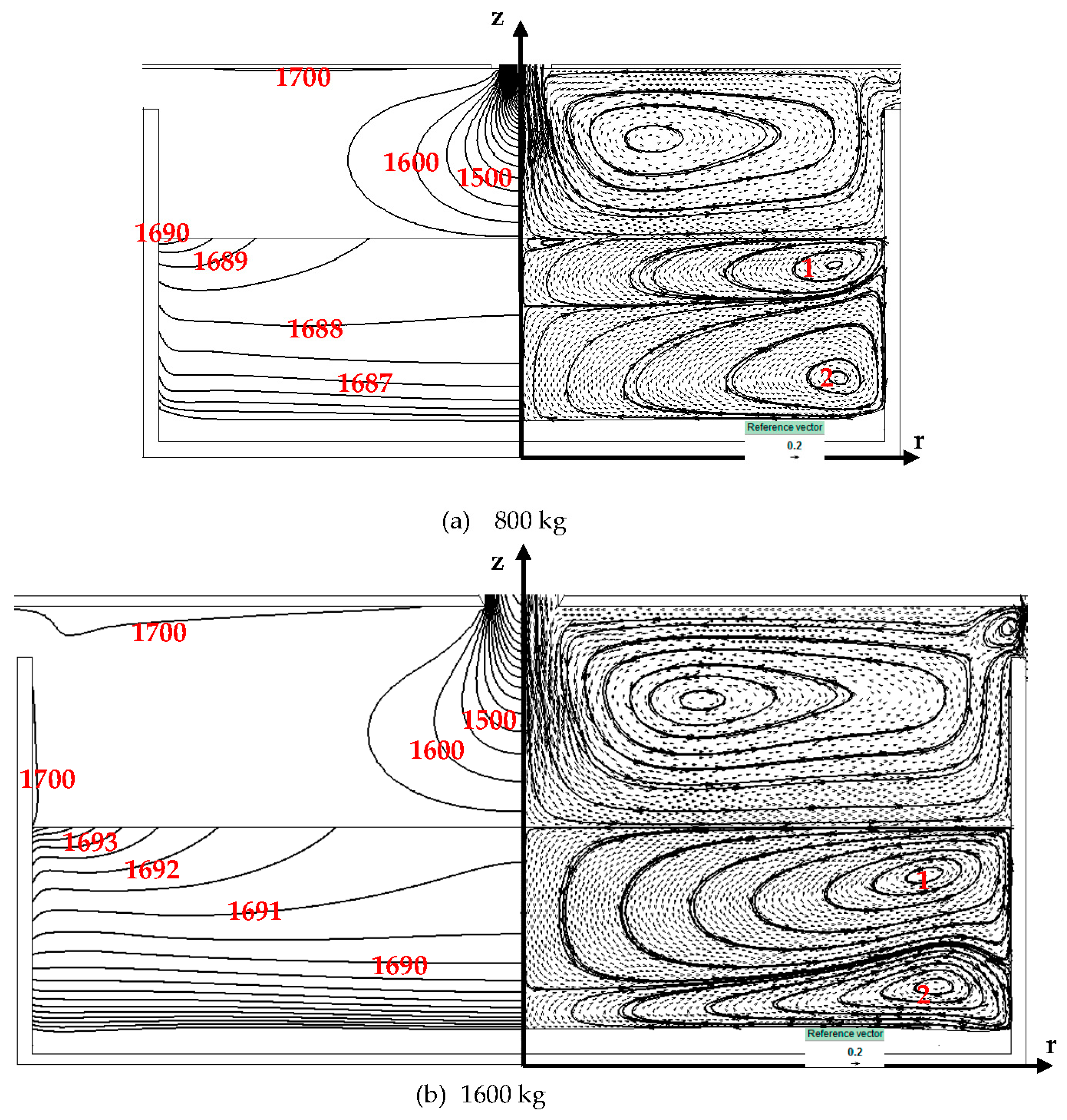
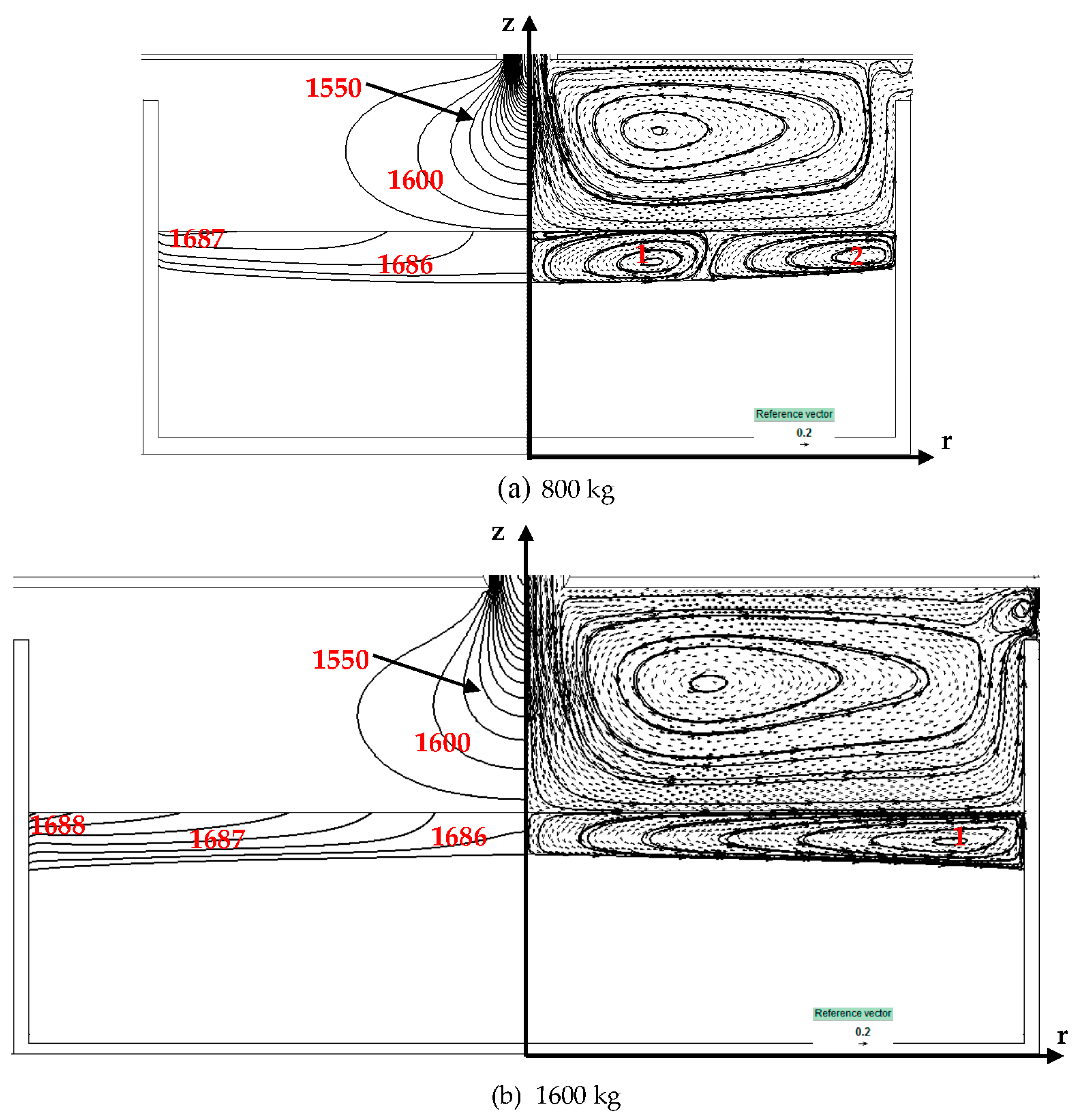
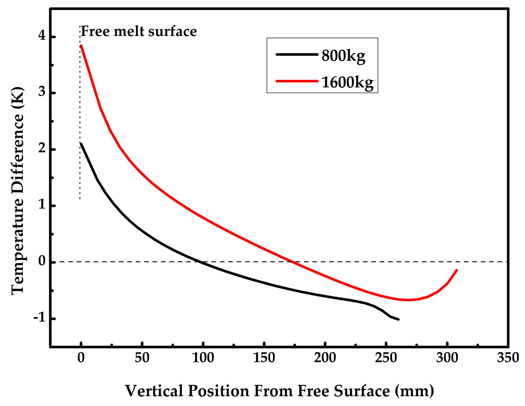
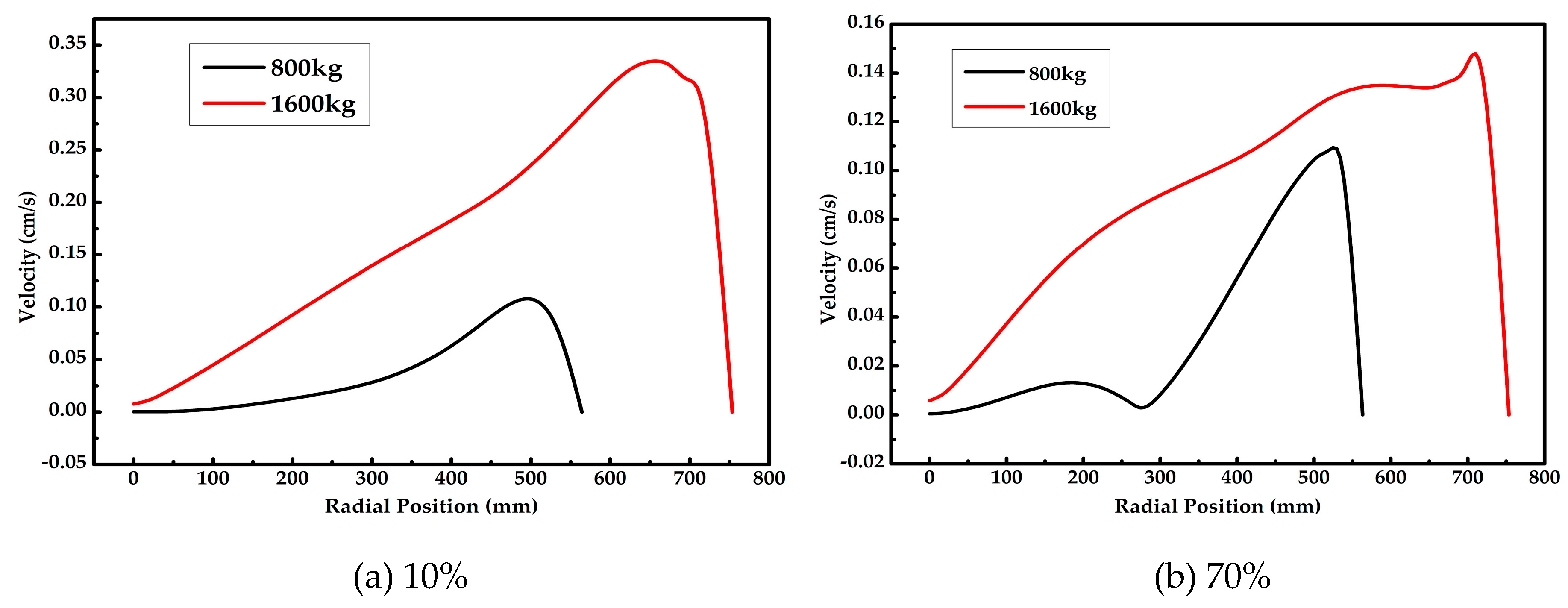
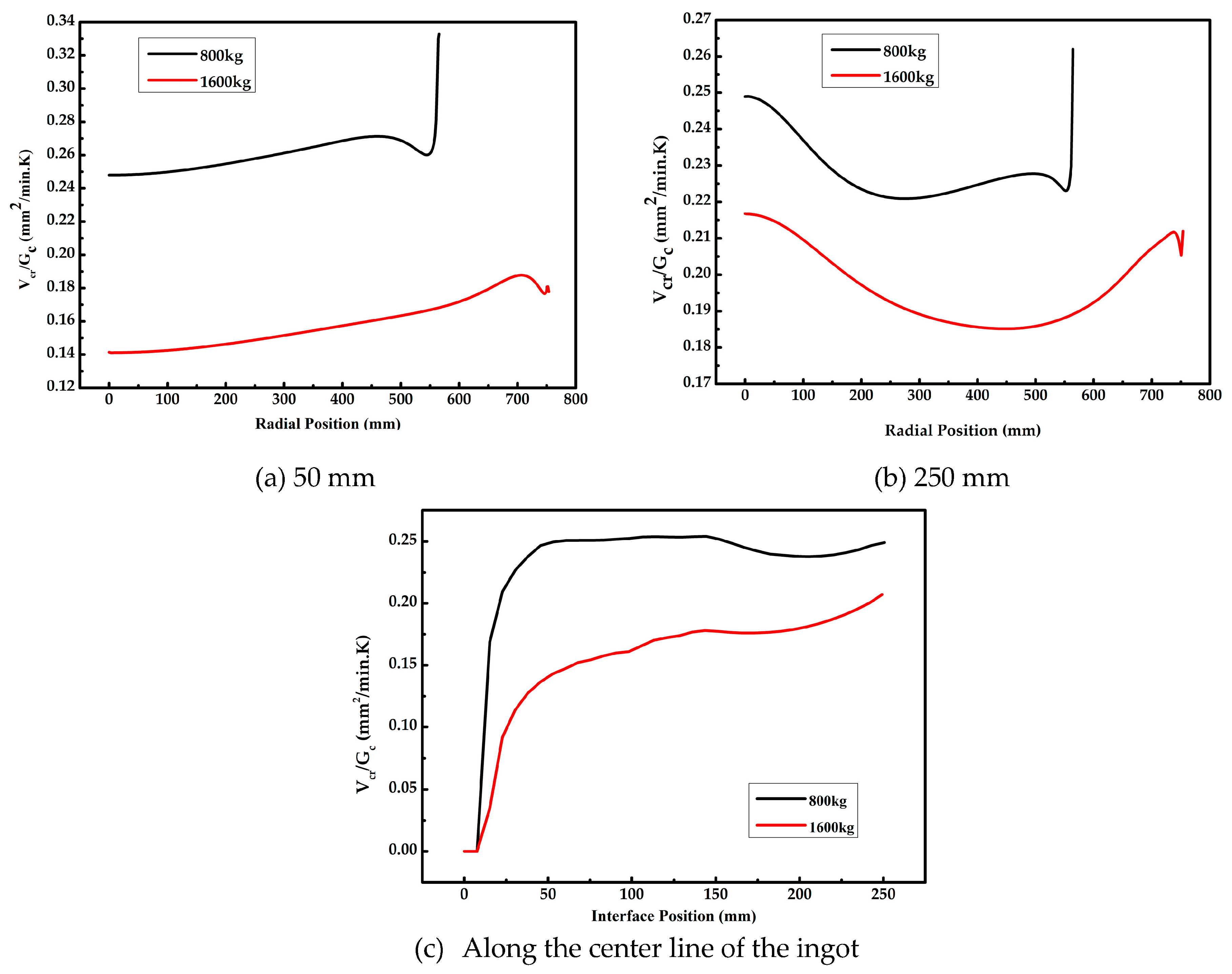
2. Results and Discussion

Numerical simulations were carried out to investigate the evolution of the thermal and flow fields during the solidification process from seed crystals of 800 kg and 1600 kg silicon feedstock. Figure 1 shows a comparison of the temperature distribution and melt flow structure at a solidification fraction of 10% for both configurations. It is clear that there are two main vortices in the silicon melt. The direction of the melt flow motion can be explained by examining Figure 2 which shows the temperature difference between the inner crucible wall and along the center line of the ingot. A positive value indicates a higher temperature at the crucible wall while a negative sign indicates a higher temperature in the central region. It can be seen that, in the upper part of the melt domain, the temperature at the crucible side wall is higher than in the central region, while it is lower in the region near the bottom of the melt. This results in the counter-clockwise motion of vortex (1) (generated by both thermo-capillary and buoyancy convection) and the clockwise motion of vortex (2) (generated by the buoyancy force). The size of cell (2) in the vertical direction was much larger than that of cell (1) for the 800 kg case, due to the existence of a negative temperature difference between the crucible wall and the center line of the ingot in a larger area of the melt, as can be seen in Figure 2. In contrast, a positive temperature difference between the crucible wall and the central region in a larger area of the melt caused cell (1) to be larger vertically than cell (2) for the 1600 kg case. It is known that heat mainly enters the melt through the upper side wall and leaves through the lower side wall and the bottom of the crucible. For the larger ingot, the power from the top and side heater was increased. This led to an increase in the temperature gradient inside the melt and, hence, the intensity of the upper vortex was also increased. The flow pattern will significantly affect the distribution of impurities along the c-m interface during the growth process. The weaker strength and smaller size of the resultant buoyancy vortex (2) helped to reduce the impurity concentration in the central region of the ingot [1].
When the silicon melt solidification fraction reached about 70% (see Figure 3a), vortex (1) moved toward the central region near the crystallization front and was reduced in size by the suppression of vortex (2). In addition, vortex (2) spread out and covered the free melt surface. For the larger-sized example, shown in Figure 3b, cell (1) completely suppressed cell (2). This suggests that the distribution of impurities at the crystallization front will be more uniform. As can be seen from a comparison of Figure 1 and Figure 3, it is clear that a lower concavity of the interface near the crucible wall can be obtained for the 1600 kg case. At a solidification fraction of 70%, in the 1600 kg case, the interface became convex to the melt. This is beneficial to the orientation of the grain boundaries outward to the crucible wall during the growth process.
Figure 4 shows the resultant velocity of the silicon melt calculated at 10 mm from the melt surface. The melt velocity increased from the center to the edge region of the ingot and was higher for the 1600 kg case. The zero value of the velocity at the end point indicated the velocity on the side inner wall of the silica crucible. The lower velocity in the central region of the melt enhanced the segregation of impurities at this part of the c-m interface. However, this effect can be reduced by maintaining the high convexity of the c-m interface in the central area during the growth process [1]. A higher convexity at the c-m interface in the central region (for the 1600 kg case) will push impurities away from the interface. Moreover, although the greater strength of cell (1) may reduce the time that impurities reside at the free surface, it can increase the capacity to carry impurities from the bottom part of the melt to the free surface. In addition, a larger area of evaporation will enhance the vaporization of impurities from the melt for the 1600 kg case.
The Voronkov ratio, Vcr/Gc, where Vcr represents the crystallization rate and Gc denotes the crystal temperature gradient normal to the c-m interface, is used to control defect formation in single crystalline silicon and mono-like silicon crystals [9]. Here, it was used to clarify the difference between the two cases. Figure 5 shows a comparison of Vcr/Gc for the two cases. As can be seen, this growth parameter was higher than the critical value (0.12 mm2/min·K [10]). In the radial direction, as presented in Figure 5a,b, Vcr/Gc became lower for the 1600 kg case when the central part of the ingot was 50 mm and 250 mm high, respectively. This indicates a lower density of defects in the mc-Si ingots. The Voronkov ratios increased with the radial position, being highest in the region near the crystal edge when the ingot height was 50 mm, due to the lower normal temperature gradient and growth rate as compared to the central part. When the growth height was 250 mm, the Voronkov parameter increased in the central region (Figure 5b). It is known that about 50 mm must be removed from the top, the bottom, and the side of an 800 kg ingot due to the poor quality of the crystal [8]. The higher value of Vcr/Gc near the side of the crystal (see Figure 5a,b) may be one of the reasons for the lower crystal quality in this region as observed in real 800 kg ingots. It can be expected that better quality can be achieved in the 1600 kg case, as suggested by the significant reduction of Vcr/Gc near the crucible wall. There was a significant change in the temperature gradient near the inner wall of the crucible with a notable variation in the shape of the c-m interface. This led to the sudden changes of Vcr/Gc in this region (Figure 5a,b) for the 800 kg case. In the 1600 kg case, however, the change of Vcr/Gc near the crucible wall became insignificant due to the reduction of the concavity of the c-m interface. Figure 5c indicates Vcr/Gc along the center line of the ingot. It is clear that the value of the Vcr/Gc ratio increased as the solidification fraction increased.

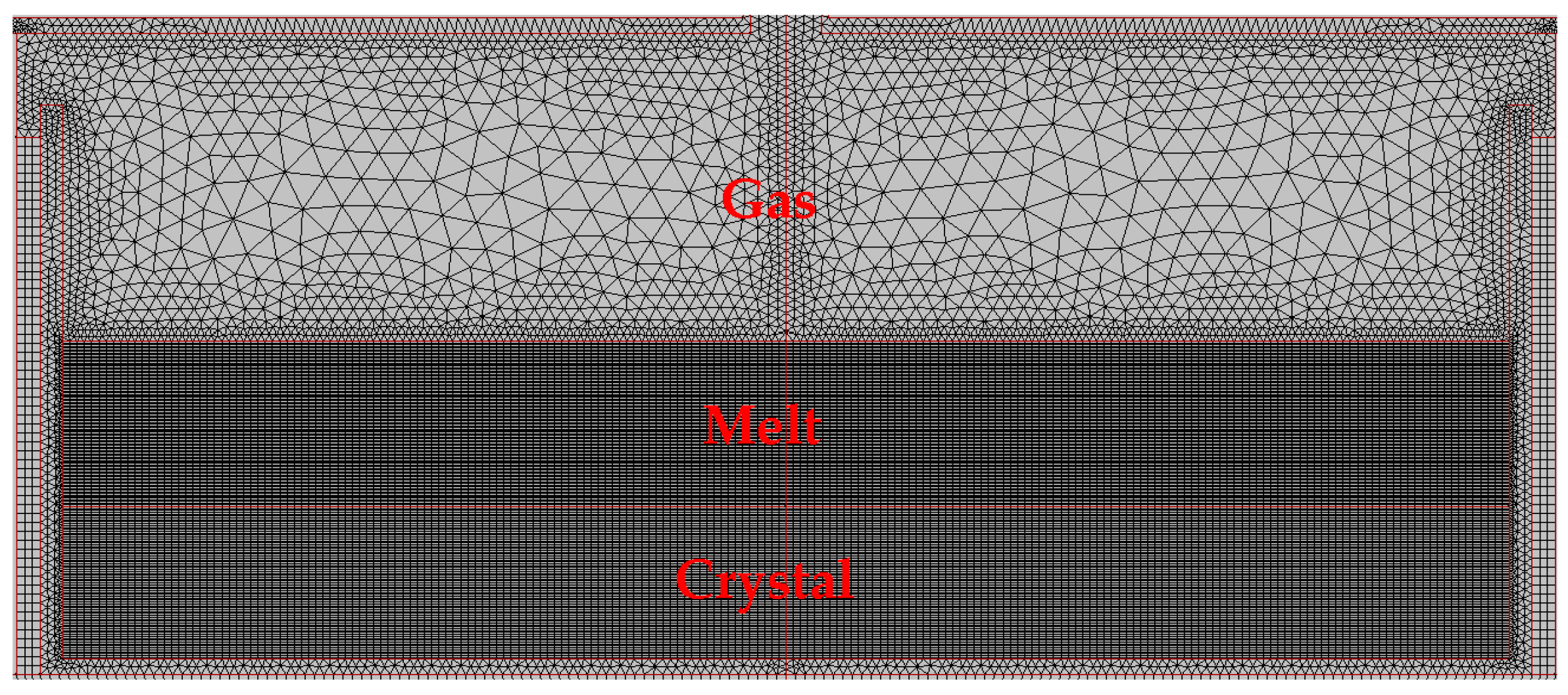
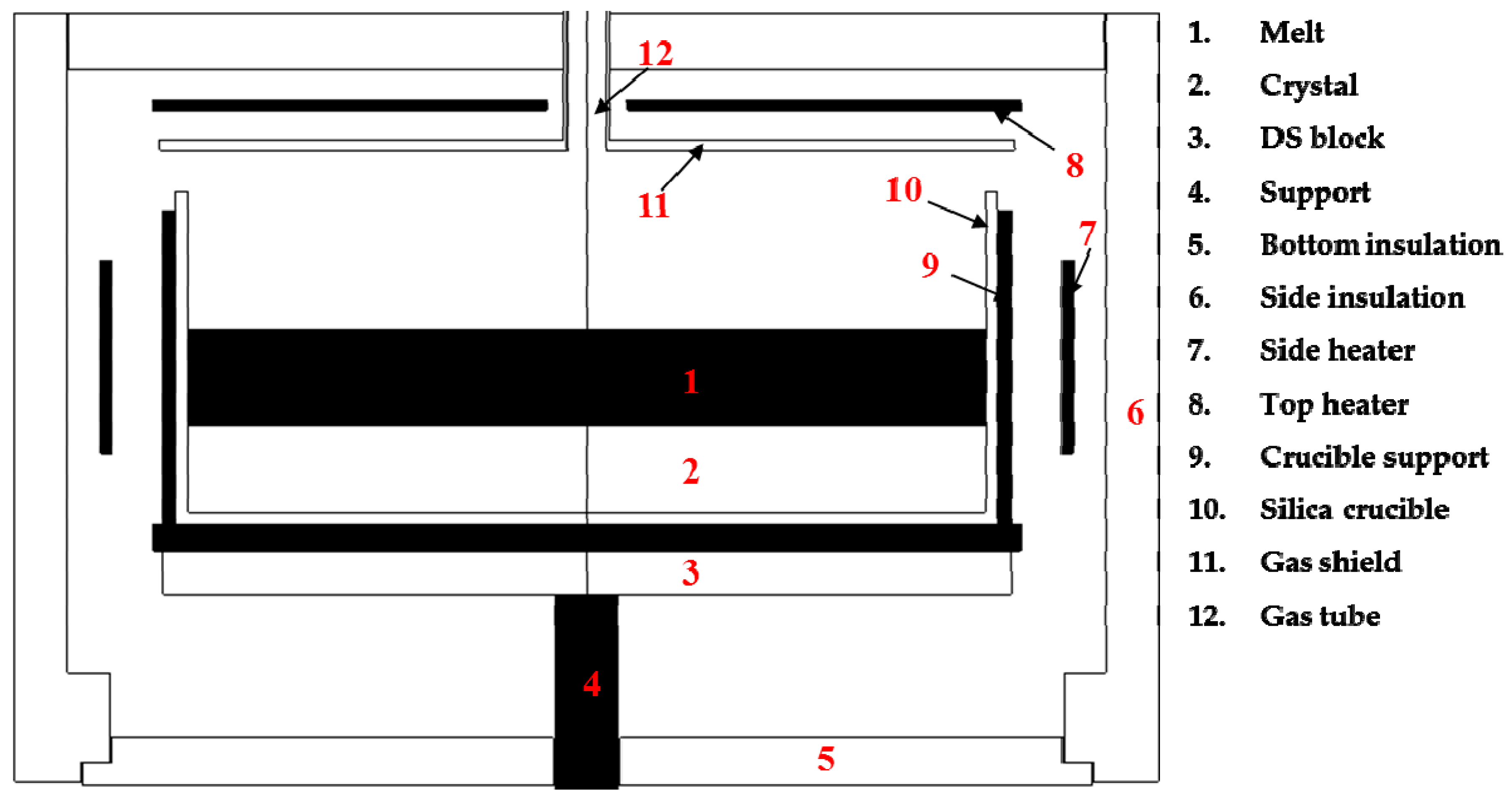
3. Materials and Methods

A series of transient global numerical simulations has been carried out to investigate changes in the thermal and flow fields of two industrial seeded DS furnaces loaded with 800 kg and 1600 kg of silicon feedstock. Figure 6 shows the major components of the industrial-scale seed DS furnace used in this study. The furnace structure for the growth of 800 kg and 1600 kg ingots is similar but the size of the furnace is much larger for the 1600 kg ingot than the 800 kg one. Thermocouple 1 (TC1) is positioned near the upper heater to monitor the temperature. TC1 indicates the target temperature used to control the output heater power. The temperature decreases with the growth time. The side insulation is moved upward during the growth process while at the bottom it remains immovable. The operational conditions such as the temperature at TC1, the power ratio between the top and the side heater, and the position of the side insulation during the growth process are different for the two cases. Due to the confidentiality policies of the company with which we are working in cooperation, the operating conditions are not specified.
It is known that performing 3D simulation will predict more exactly the evolution of flow and thermal field during the growth of ingot [6,11,12]. However, 3D modeling is complex and time consuming, especially for the large size of ingot and the transient computation. To predict the evolution of defect from the history of interface shape, temperature, and crystallization rate, the transient global model taking into account the thermal conduction, thermal radiation, melt convection and gas flow during the real growth process should be used. A huge computational power is needed to perform a transient 3D simulation in a real growth process. Due to this limitation, in the present work, the real configuration of a DS furnace, with its square crucible, is replaced by a 2D axially-symmetric model which is cylindrical in shape. This simplification has been used by many researchers [1,2,3,4,5,8,13,14,15,16,17]. The simulation results have also been validated by comparison with experimental results [3,16,17]. In this study, the real growth process provided by Sino-American Silicon Products Inc. (SAS, Taiwan) is adopted. The CGSim (Crystal Growth software) program package developed by the Semiconductor Technology Research (STR) Group, which is based on the Finite Volume Method (FVM), is used for all computations discussed in this paper. The grid distribution inside the crucible system is described in Figure 7. The Reynolds-averaged Navier-Stoke (RANS) equations with one equation model are employed to calculate the transient regime in the melt flow. The Wolfshtein model is applied to catch the proper increase in the dissipation rate near the wall given the buoyancy flow in the transient regime. The Si melt is considered to be a Newtonian fluid while the inert argon gas is considered an ideal gas. The effects of deformation of the melt-gas surface are neglected in this study to simplify the calculation.
The governing equations for the fluid flow and heat transfer are written as follows:
For the fluid flow:
ρ i t + ( ρ i u i ) = 0 ;
ρ i u i t + ( u i ) ρ i u i = p i + τ i + ( ρ i ρ i , 0 ) g ;
ρ i C p i T i t + ( C p i ρ i u i T i ) = ( k i T i ) ,
where ρ, ρ0, Cp, u, τ, g, T, and k are the density, reference density, specific heat, velocity, stress tensor, gravitational acceleration, temperature, and thermal conductivity, respectively. Subscript i represents argon gas (g) or liquid silicon (l).
For the heater:
( ρ h C p h T h ) t = ( k h T h ) + q ˙ ,
where q ˙ is the heat generation from the heater. Subscript h indicates the heater component.
The thermal conditions on the interface between two opaque surfaces are
( k T n ) 1 = ( k T n ) 2 ;
T 1 = T 2 .
The radiative heat transfer along the interface between the opaque surface and gas is as follows:
( k T n ) o p a q u e = ( k T n ) g a s + σ s ε T 4 q i n ;
where σs is the Stefan-Boltzmann constant, ε is the thermal emissivity and qin is the incoming radiative heat flux. Along the free surface, the normal velocity component is set to zero while the tangential velocity one should satisfy the Marangoni condition:
μ l u τ l n = μ g u τ g n + σ T τ T ,
where μ is the dynamic viscosity; n and τ are the normal and tangential directions to the free surface, respectively; σ is the surface tension of the silicon melt. The boundary conditions for the flow velocity at the solid walls are as follows: the velocity component in the normal direction to the wall is set to zero, while that in the tangential direction is equal to the wall velocity. The position of the c-m interface is adjusted during the growth process to satisfy the Stefan condition given by
ρ c r y s t u n Δ H = ( k T n ) c r y s t ( k T n ) m e l t ,
T = T m e l t ,
where ρcryst is the crystal density; un is the local crystalline rate normal to the c-m interface; and ΔH is the latent heat. The temperature at the crystallization front is considered to be the melting temperature of silicon, 1685 K. The physical properties of the materials used in the present study have been detailed in our previous papers [1,14,15].

4. Conclusions

A series of 2D transient numerical simulations was carried out to investigate the thermal and flow fields inside a seeded DS furnace for the growth of mc-Si crystals, for both 800 kg and 1600 kg feedstock. The results show that the 1600 kg ingot grown by the G8 furnace may be of higher quality than the 800 kg ingot grown by the G6 furnace. There are differences in the structure of the melt flow during the growth process. In the 1600 kg case, the size and the strength of the upper cell (1), which is generated by both the buoyancy and thermocapillary force, were much larger than the lower one (2), generated by only the buoyancy force. The opposite is true for the 800 kg case. There is a reduction in the concavity of the c-m interface near the crucible wall and an increase in the convexity of the interface at higher solidification fractions for the 1600 kg case. Moreover, the Voronkov ratios, which indicate the formation of defects, are lower during the solidification process for the 1600 kg case. It is also worth emphasizing that a 3D time-dependent numerical study should be conducted to investigate the growth of large-sized silicon ingots. The difference in the flow structure of silicon melts between the two cases (800 kg and 1600 kg) may be more significant with 3D modeling.

Acknowledgments

The authors would like to thank the Bureau of Energy, Ministry of Economic Affairs, Republic of China, for their support of this study.

Author Contributions

Chun Hung Chen, Yen Hao Huang, Huang Wei Lin, Andy Yu, Bruce Hsu, Michael Yang, and Ray Yang provided the information about the furnace structure and operating conditions for crystal growth. Thi Hoai Thu Nguyen, Jyh Chen Chen, and Chieh Hu developed the mathematical model, performed the numerical simulations, and analyzed the results. All authors took part in the writing and discussion processes.

Conflicts of Interest

The authors declare no conflict of interest.

References

  1. Teng, Y.Y.; Chen, J.C.; Lu, C.W.; Chen, C.Y. The carbon distribution in multicrystalline silicon ingots grown using the directional solidification process. J. Cryst. Growth 2010, 312, 1282–1290. [Google Scholar] [CrossRef]
  2. Yu, Q.; Liu, L.; Ma, W.; Zhong, G.; Huang, X. Local design of the hot zone in an industrial seeded directional solidification furnace for quasi-single crystalline silicon ingots. J. Cryst. Growth 2012, 358, 5–11. [Google Scholar] [CrossRef]
  3. Ding, C.; Huang, M.; Zhong, G.; Ming, L.; Huang, X. A design of crucible susceptor for the seeds preservation during a seeded directional solidification process. J. Cryst. Growth 2014, 387, 73–80. [Google Scholar] [CrossRef]
  4. Nguyen, T.H.T.; Liao, S.H.; Chen, J.C.; Chen, C.H.; Huang, Y.H.; Yang, C.J.; Lin, H.W.; Nguyen, H.B. Effects of the hot zone design during the growth of large size multi-crystalline silicon ingots by the seeded directional solidification process. J. Cryst. Growth 2016, 452, 27–34. [Google Scholar] [CrossRef]
  5. Wu, Z.; Zhong, G.; Zhou, X.; Zhang, Z.; Wang, Z.; Chen, W.; Huang, X. Upgrade of the hot zone for large-size high-performance multi-crystalline silicon ingot casting. J. Cryst. Growth 2016, 441, 58–64. [Google Scholar] [CrossRef]
  6. Dropka, N.; Ervik, T.; Czupalla, M.; Kiessling, F.M. Scale up aspects of directional solidification and Czochralski silicon growth processes in traveling magnetic fields. J. Cryst. Growth 2016, 451, 95–102. [Google Scholar] [CrossRef]
  7. Lan, C.W.; Yang, C.F.; Lan, A.; Yang, M.; Yu, A.; Hsu, H.P.; Hsu, B.; Hsu, C. Engineering silicon crystal for photovoltaics. CrystEngComm 2016, 18, 1474–1485. [Google Scholar] [CrossRef]
  8. Nguyen, T.H.T.; Chen, J.C.; Hu, C.; Chen, C.H.; Huang, Y.H.; Lin, H.W.; Yu, A.; Hsu, B. Numerical analysis of thermal stress and dislocation density distributions in large size multi-crystalline silicon ingots during the seeded growth process. J. Cryst. Growth 2016. In Press. [Google Scholar] [CrossRef]
  9. Black, A.; Medina, J.; Pineiro, A.; Dieguez, E. Optimizing seeded casting of mono-like silicon crystals through numerical simulation. J. Cryst. Growth 2012, 353, 12–16. [Google Scholar] [CrossRef]
  10. Voronkov, V.; Falster, R. Vacancy and self-interstitial concentration incorporated into growing silicon crystals. J. Appl. Phys. 1999, 56, 5975. [Google Scholar] [CrossRef]
  11. Vizman, D.; Friedrich, J.; Mueller, G. 3D time-dependent numerical study of the influence of the melt flow on the interface shape in a silicon ingot casting process. J. Cryst. Growth 2007, 303, 231–235. [Google Scholar] [CrossRef]
  12. Vizman, D.; Dadzis, K.; Friedrich, J. Numerical parameter studies of 3D melt flow and interface shape for directional solidification of silicon in a travelling magnetic field. J. Cryst. Growth 2013, 381, 169–178. [Google Scholar] [CrossRef]
  13. Liu, L.; Yu, Q.; Qi, X.; Zhao, W.; Zhong, G. Controlling solidification front shape and thermal stress in growing quasi-single-crystal silicon ingots: Process design for seeded directional solidification. J. Appl. Therm. Eng. 2015, 91, 225–233. [Google Scholar] [CrossRef]
  14. Teng, Y.Y.; Chen, J.C.; Huang, B.S.; Chang, C.H. Numerical simulation of impurity transport under the effect of a gas flow guidance device during the growth of multicrystalline silicon ingots by the directional solidification process. J. Cryst. Growth 2014, 385, 1–8. [Google Scholar] [CrossRef]
  15. Teng, Y.Y.; Chen, J.C.; Lu, C.W.; Chen, H.I.; Hsu, C.; Chen, C.Y. Effects of the furnace pressure on oxygen and silicon oxide distributions during the growth of multicrystalline silicon ingots by the directional solidification process. J. Cryst. Growth 2011, 318, 224–229. [Google Scholar] [CrossRef]
  16. Ma, W.; Zhong, G.; Sun, L.; Yu, Q.; Huang, X.; Liu, L. Influence of an insulation partition on a seeded directional solidification process for quasi-single crystalline silicon ingot for high efficiency solar cells. Sol. Energy Mater. Sol. Cells 2012, 100, 231–238. [Google Scholar] [CrossRef]
  17. Wu, Z.; Zhong, G.; Zhang, Z.; Zhou, X.; Wang, Z. Optimization of the high performance multicrystalline silicon solidification process by insulation partition design using transient global simulations. J. Cryst. Growth 2015, 426, 110–116. [Google Scholar] [CrossRef]
Figure 1. Distribution of temperature (left, ∆T = 0.5 K (in melt), ∆T = 50 K (in gas)) and flow structure (right) in the silicon melt and argon gas at a solidification fraction of 10% with different silicon feedstock capacities: (a) 800 kg; (b) 1600 kg.
Crystals 07 00074 g001
Figure 2. Comparison of temperature differences between the crucible side wall and the central region of the melt at a solidification fraction of 10%.
Crystals 07 00074 g002
Figure 3. Distribution of temperature (left, ∆T = 0.5 K (in melt), ∆T = 50 K (in gas)) and flow structure (right) in the silicon melt and argon gas at a solidification fraction of 70% with different silicon feedstock capacities: (a) 800 kg; (b) 1600 kg.
Crystals 07 00074 g003
Figure 4. Comparison of the resultant velocity of the silicon melt at 10 mm under the free melt surface with different solidification fractions: (a) 10%; (b) 70%.
Crystals 07 00074 g004
Figure 5. Comparison of Vcr/Gc in the radial direction at crystal heights of 50 mm (a) and 250 mm (b), and in the vertical direction along the center line of the ingot (c).
Crystals 07 00074 g005
Figure 6. Configuration of the major components of an industrial DS system.
Crystals 07 00074 g006
Figure 7. Distribution of grid inside the crucible system.
Crystals 07 00074 g007

