Article

The Influence of Conductive Nanodomain Walls on the Photovoltaic Effect of BiFeO3 Thin Films

State Key Laboratory of ASIC & System, School of Microelectronics, Fudan University, Shanghai 200433, China
*
Author to whom correspondence should be addressed.
Crystals 2017, 7(3), 81; https://doi.org/10.3390/cryst7030081
Submission received: 30 January 2017 / Revised: 26 February 2017 / Accepted: 6 March 2017 / Published: 21 March 2017
(This article belongs to the Special Issue Multiferroics Crystals)

Abstract

:
Two Planar Pt electrodes with an inter-electrode distance of about 100 nm were fabricated at the surface of BiFeO3 thin films, which allow the manipulation of ferroelectric domain switching at nanoscale. This electrode configuration was pursued to study conductive domain-wall influence on the photovoltaic current in BiFeO3 thin films. Modulations of short-circuit photovoltaic current and hysteretic conductive switching behaviors were found in the above nanodevices, accompanied by the generation of the conductive domain walls connecting two gapped electrodes. Our technique provides a new method to configure ferroelectric domains, where the influence of the conductive domain walls on the photovoltaic effect is preeminent.

1. Introduction

The photovoltaic (PV) effect in ferroelectrics has attracted great attention in recent years because of the intriguing physics underpinning this phenomenon and its potential applications in sensors, nonvolatile memories, and solar cells [1,2,3,4,5]. Among ferroelectrics, lead-free BiFeO3 (BFO) is a promising candidate for the study of the PV effect, due to its relatively narrow band gap of 2.6–2.8 eV [6,7,8,9]. Normally, two different geometrical configurations of capacitor electrodes were used to study the nucleating and switching dynamics of domains and domain walls (DWs) on the PV effect. The first geometry mostly adopts the parallel capacitor-like configuration of top and bottom electrodes, where the electrodes are easier to fabricate. However, the nucleating domains embedded between the two electrodes under an electric field are quite difficult to image using piezoresponse force microscopy (PFM), due to the capped top electrode. Moreover, the stressing differences near the top and bottom electrode layers caused by lattice mismatching between the film and substrate, as well as the uneven distribution of oxygen vacancies near the two electrodes in the formation of interfacial passive layers are also believably significant, making the clear determination of various PV effects elusive [10,11]. In comparison, the latter geometry of symmetrical in-plane electrode configuration allows direct observation of domains between the two electrodes by PFM, where an anisotropic PV effect was also found in BFO [12,13]. This anisotropy is believably associated with the periodically distributed DWs, which have proven to be more conductive than the surrounding bulk in BFO [14]. In recent years, several workers have attempted to exploit this advantage to disentangle the influence of conductive DWs on the PV effect by fabricating planar electrodes with different geometries of a few micrometers to millimeters on BFO thin films innate with periodic stripe domain patterns [12,13,14,15]. However, it is hard to distinguish the discrete PV contributions of ferroelectric individual domains and conductive DWs set up in such macroscopic geometries. It would be of great value to develop new methods to capture a nucleating domain at the nanoscale. This work is aimed to that target.
In this article, we fabricated two planar Pt electrodes separated with a nanogap of 100 nm at the surface of BFO thin films to manipulate individual ferroelectric domain motion as well as the formation of DWs at nanoscale. The quick decay of short-circuit photovoltaic current (Isc) corresponding with enhanced conductance can be observed when the DWs appear to electrically shorten the two planar electrodes.

2. Experimental Details

The smooth (001) BFO thin films in a thickness of 120 nm were epitaxially deposited on GdScO3 (GSO) (110) single-crystal substrates by a pulsed laser deposition (PLD) technique. The substrate temperature was 893 K, and the oxygen partial pressure was 10 Pa. After the film deposition, two 30 nm-thick planar Pt electrodes (TE1 and TE2) with an inter-electrode distance of about 100 nm were patterned by electron beam lithography (EBL) and ion milling using Cr mask layers. The edges of the electrodes were parallel to the domain walls.
The crystal structure of the BFO thin films were studied using X-ray diffraction (XRD, D8 Advance with Cu-Kα radiation, Bruker, Karlsruhe, Germany). Morphology and ferroelectric domain configuration of the films were imaged by atomic force microscopy (AFM) and piezoresponse force microscopy (PFM, Bruker Icon), respectively. The as-formed nanodevices were checked using scanning electron microscope (SEM, Zeiss Sigma HD, Jena, Germany). The current–voltage (IV) tests and Isc measurements were carried out using a semiconductor analyzer (B1500A, Agilent, San Francisco, CA, USA). An ultraviolet laser with wavelength of 375 nm (in energy density of 100 mW/cm2) was used as an excitation light source for photoelectric measurements. All voltages were applied on TE1 with TE2 grounded, and all measurements were carried out at room temperature.
To investigate the impact of conductive DWs on the PV effect, a pre-poling voltage was applied to polarize ferroelectric domains within the gap between the two electrodes. After that, the Isc and IV curves were measured under laser illumination, and PFM measurements were carried out to image the corresponding ferroelectric domains. Later, we repeated the above measurements in step-by-step increase in pre-poling voltage from −8 V to 9 V.

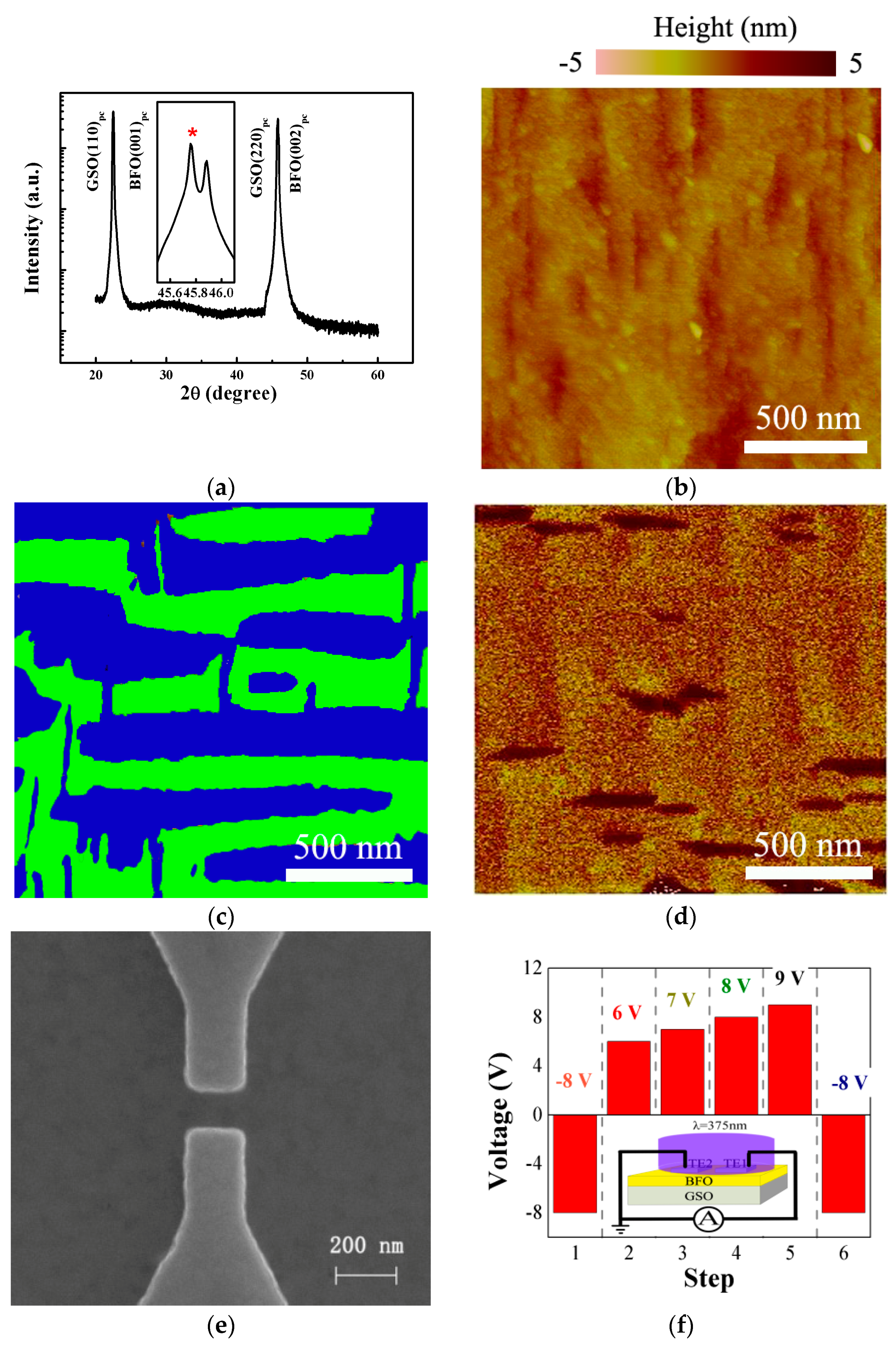
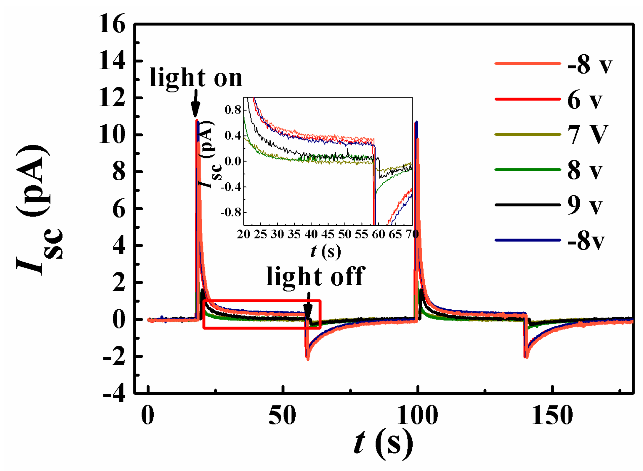
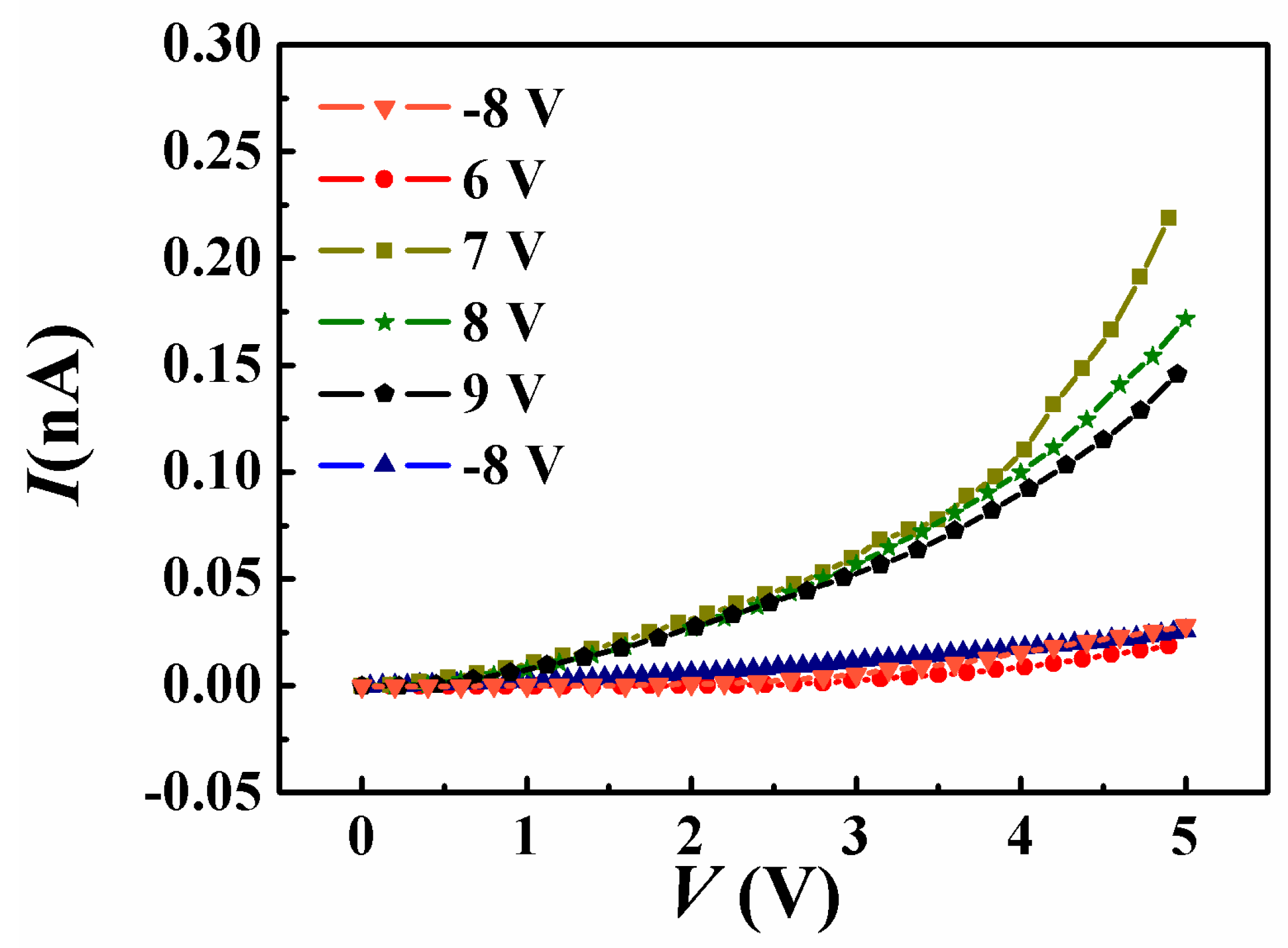
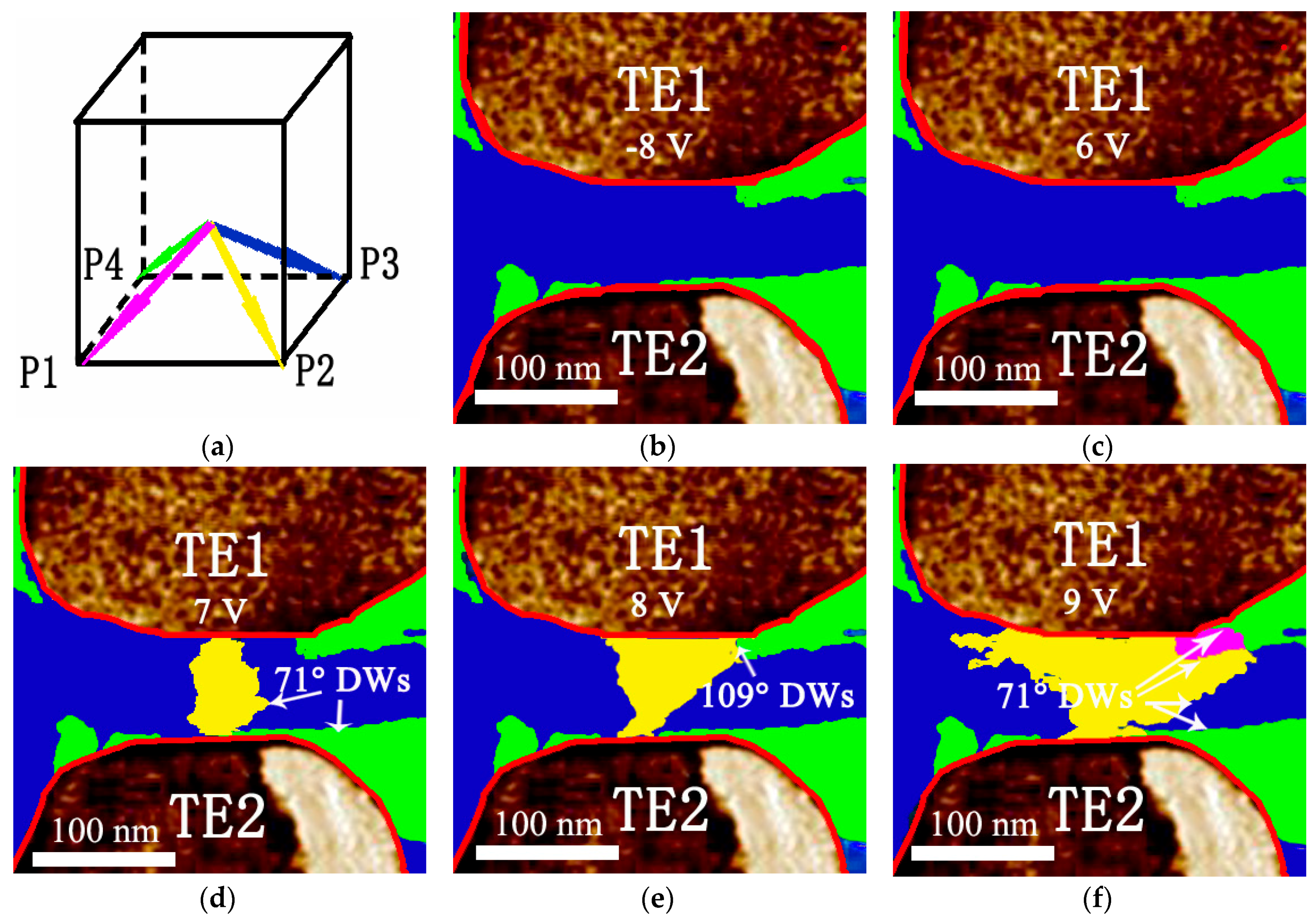
3. Results and Discussion

Figure 1a shows the XRD θ–2θ scan of the BFO thin films. All strong peaks can be indexed to major BFO (00l)pc reflections in a pseudocubic phase symmetry, indicating a pure BFO perovskite phase. The overlapping reflections of BFO (002)pc and GSO (220)pc can be discerned by a high-resolution XRD pattern, as shown in the inset. Figure 1b shows the surface morphology of the BFO thin films by an AFM image. This photograph demonstrates that the BFO thin films have a smooth surface with a root-mean-square roughness of 0.405 nm. The in-plane piezoelectric phase image in Figure 1c confirms the ordered 71° ferroelectric domains and DWs in the as-grown states, and the out-of-plane PFM image in Figure 1d nevertheless indicates a uniform downward polarization pointing to the substrate. This preferred downward polarization has been widely reported in previous studies in BFO thin films [16,17,18]. Figure 1e shows the SEM photograph of the as-formed nanodevice, indicating a gap length of 100 nm in width of 200 nm. The test order of our stepped electrical measurements is illustrated in Figure 1f.
Time-dependent Isc curves for the nanodevice with pre-poling voltages increasing from −8 V to 9 V are shown in Figure 2. Each Isc value increases rapidly up to the maxima at the moment when the laser is turned on. Later, the Isc value decreases in a few seconds until leveling off at a constant value. The inset demonstrates the stabilized Isc values extracted from each step, indicating that all stabilized Isc values are positive. The Isc values with pre-poling voltages below 6 V are around 400 fA in steps 1 and 2. However, a sudden decrease of Isc value can be observed when the pre-poling voltage is increased up to 7 V. After the further increase of the pre-poling voltage lager than 7 V, the Isc value stabilizes at around 0 fA and becomes less sensitive to the pre-poling voltages. When the pre-poling voltage is decreased to −8 V in the last step, the Isc value can be rejuvenated back to 400 fA again. This repeatable switching behavior of Isc—which is attractive for potential application in nonvolatile memories—is pertinent to the ferroelectric polarization switching [4,19].
According to the report by Bhatnagar and coworkers [14], the PV effect in BFO films is extremely sensitive to photoconductivity under light illumination. With this consideration, our IV tests were carried out after the Isc measurements in each step. Figure 3 shows the IV curves of the nanodevice with pre-poling voltage increasing from −8 V to 9 V. The nanodevice demonstrates a low conductance state in steps 1 and 2 where the pre-poling voltages are −8 V and 6 V, respectively. However, the conductance of the nanodevice switches from a low conductance state to a high conductance state in steps 3 to 5, where the pre-poling voltage is larger than 6 V. In the last step, the pre-poling voltage turns back to −8 V, and the conductance of the nanodevice again switches down to a low conductance state. This result along with the Isc measurements confirms that the Isc is closely coupled to the photoconductivity. In addition, the conductance reaches its maximum when the pre-poling voltage is 7 V. After that, it decreases slightly with increasing pre-poling voltage.
In previous studies, conductive switching behaviors were believably associated with polarization rotations in ferroelectrics along with either the change of barrier heights at two ferroelectric/metal interfaces or the formation of conductive DWs [20,21,22,23]. Hence, PFM measurements need to be performed to confirm the evolution of the ferroelectric domain configuration with different pre-poling voltages. For the convenience, we defined the possible polarization variants of the BFO thin film as P1, P2, P3, and P4, as shown in Figure 4a. Figure 4b–f show four main polarizations within the nanogap, and the configurations show most of 71° DWs. Figure 4b shows the domain configuration in step 1, indicating a uniform P3 between the two electrodes. The domain configuration in step 2 is similar to that in step 1, indicating that no new domain is formed. However, when the pre-poling voltage is increased to 7 V, P2 along with 71° DWs is formed (as shown in Figure 4d), demonstrating an apparent planar coercive electric field of 700 kV/cm which is much larger than the 200 kV/cm in our previous reports [24]. This difference stems from different configuration of electrodes. The behaviors of polarization reversal (P3 switches to P2 and P4 switches to P1) in the PFM images also reveal that the in-plane polarization only rotates along the direction of the applied electric filed in our experiments and that the formation of 109° DWs in Figure 4e should also be attributed to 71° rotation of P3. Moreover, the area of P2 and the length of 71° DWs both increase with increasing pre-poling voltage.
The results in Figure 2 and Figure 3 can be well understood by the evolution of ferroelectric domains and conductive DWs with stepped voltages. Because the 71° DWs in BFO thin films have been proven to be more conductive than the surrounding bulk [25], the two planar electrodes electrically shortened by 71° DWs can be responsible for the enhanced conductance in Figure 3. The slight decrease of conductance in higher pre-poling voltages can be attributed to increasing length of 71° DWs. The 71° DWs connecting the two planar electrodes act as shunt resistors, which reduce the photocurrent generated by the ferroelectric matrix. This is a possible mechanism for the Isc decrease. Moreover, the Isc is stable at around 0 pA with pre-poling voltage larger than 6 V, though the area of P2 varies considerably. This result indicates that the conductive DWs are dominative factors to depress the generated photocurrent. For this reason, the periodic stripe DWs can result in an anisotropic PV effect in BFO.

4. Conclusions

We fabricated planar Pt electrodes with an inter-electrode distance of about 100 nm at the surface of BFO thin films, which allow the manipulation of conductive 71° DWs by applying various pre-poling voltages. From the PV measurements, we found that the Isc is extremely sensitive to the pre-poling voltage. At a bisection voltage lower/larger than 6 V, the Isc value is about 400 fA/0 fA. It is believed that formation of conductive DWs electrically shortening the two planar electrodes is responsible for this difference. This is in agreement with the DW evolution with the pre-poling voltage from our PFM characterization. Undoubtedly, our work provides the strategy to disentangle the mechanism of the PV effect from conductive DWs in ferroelectrics, where the periodic stripe conductive DWs dominate the anisotropic PV effect.

Acknowledgments

This work was supported by the National Key Basic Research Program of China (grant number 2014CB921004) and the National Natural Science Foundation of China (grant number 61674044).

Author Contributions

Zilong Bai performed the experiments and wrote the paper; Yan Zhang and Huizhen Guo prepared the samples; Anquan Jiang contributed reagents/materials/analysis tools.

Conflicts of Interest

The authors declare no conflict of interest.

References

  1. Xing, J.; Guo, E.; Dong, J.; Hao, H.; Zheng, Z.; Zhao, C. High-sensitive switchable photodetector based on BiFeO3 film with in-plane polarization. Appl. Phys. Lett. 2015, 106, 033504. [Google Scholar] [CrossRef]
  2. Lotey, G.S.; Verma, N.K. Gd-doped BiFeO3 nanoparticlesv—A novel material for highly efficient dye-sensitized solar cells. Chem. Phys. Lett. 2013, 574, 71–77. [Google Scholar] [CrossRef]
  3. Keskin, V.; Gupta, A.; Szulczewski, G. Solution processed TiO2/BiFeO3/poly(3-hexylthiophene) solar cells. Mater. Lett. 2015, 159, 305–308. [Google Scholar] [CrossRef]
  4. Guo, R.; You, L.; Zhou, Y.; Lim, Z.S.; Zou, X.; Chen, L.D.; Ramesh, R.; Wang, J. Non-volatile memory based on the ferroelectric photovoltaic effect. Nat. Commun. 2013, 4, 1990. [Google Scholar] [CrossRef]
  5. Katiyar, R.K.; Misra, P.; Sahoo, S.; Morell, G.; Katiyar, R.S. Enhanced photoresponse in BiFeO3/SrRuO3 heterostructure. J. Alloy. Compd. 2014, 609, 168–172. [Google Scholar] [CrossRef]
  6. Ihlefeld, J.F.; Podraza, N.J.; Liu, Z.K.; Rai, R.C.; Xu, X.; Heeg, T.; Chen, Y.B.; Li, J.; Collins, R.W.; Musfeldt, J.L. Optical band gap of BiFeO3 grown by molecular-beam epitaxy. Appl. Phys. Lett. 2008, 92, 142908. [Google Scholar] [CrossRef]
  7. Hauser, A.J.; Zhang, J.; Mier, L.; Ricciardo, R.A.; Woodward, P.M.; Gustafson, T.L.; Brillson, L.J.; Yang, F.Y. Characterization of electronic structure and defect states of thin epitaxial BiFeO3 films by UV-visible absorption and cathodoluminescence spectroscopies. Appl. Phys. Lett. 2008, 92, 222901. [Google Scholar] [CrossRef]
  8. Clark, S.J.; Robertson, J. Energy levels of oxygen vacancies in BiFeO3 by screened exchange. Appl. Phys. Lett. 2009, 94, 022902. [Google Scholar] [CrossRef] [Green Version]
  9. Ji, W.; Yao, K.; Liang, Y.C. Bulk Photovoltaic Effect at Visible Wavelength in Epitaxial Ferroelectric BiFeO3 Thin Films. Adv. Mater. 2010, 22, 1763–1766. [Google Scholar] [CrossRef]
  10. Matsuo, H.; Kitanaka, Y.; Inoue, R.; Noguchi, Y.; Miyayama, M. Cooperative effect of oxygen-vacancy-rich layer and ferroelectric polarization on photovoltaic properties in BiFeO3 thin film capacitors. Appl. Phys. Lett. 2016, 108, 32901. [Google Scholar]
  11. Matsuo, H.; Kitanaka, Y.; Inoue, R.; Noguchi, Y.; Miyayama, M. Switchable diode-effect mechanism in ferroelectric BiFeO3 thin film capacitors. J. Appl. Phys. 2015, 118, 114101. [Google Scholar] [CrossRef]
  12. Nakashima, S.; Uchida, T.; Nakayama, D.; Fujisawa, H.; Kobune, M.; Shimizu, M. Bulk photovoltaic effect in a BiFeO3 thin film on a SrTiO3 substrate. Jpn. J. Appl. Phys. 2014, 53, 09PA16. [Google Scholar] [CrossRef]
  13. Nakashima, S.; Uchida, T.; Takayama, K.; Fujisawa, H.; Shimizu, M. Influence of the polarization direction of light on the anomalous photovoltaic effect in BiFeO3 thin films. J. Korean Phys. Soc. 2015, 66, 1389–1393. [Google Scholar] [CrossRef]
  14. Bhatnagar, A.; Chaudhuri, A.R.; Kim, Y.H.; Hesse, D.; Alexe, M. Role of domain walls in the abnormal photovoltaic effect in BiFeO3. Nat. Commun. 2013, 4, 2835. [Google Scholar] [CrossRef] [Green Version]
  15. Yang, S.Y.; Seidel, J.; Byrnes, S.; Shafer, P.; Yang, C.H.; Rossell, M.D.; Yu, P.; Chu, Y.H.; Scott, J.F.; Ager, J.W. Above-bandgap voltages from ferroelectric photovoltaic devices. Nat. Nanotechnol. 2010, 5, 143–147. [Google Scholar] [CrossRef] [PubMed]
  16. Lee, D.; Baek, S.H.; Kim, T.H.; Yoon, J.G.; Folkman, C.M.; Eom, C.B.; Noh, T.W. Polarity control of carrier injection at ferroelectric/metal interfaces for electrically switchable diode and photovoltaic effects. Phys. Rev. B 2011, 84, 12. [Google Scholar] [CrossRef]
  17. Baek, S.H.; Jang, H.W.; Folkman, C.M.; Li, Y.L.; Winchester, B.; Zhang, J.; He, Q.; Chu, Y.; Nelson, C.T.; Rzchowski, M.S. Ferroelastic switching for nanoscale non-volatile magnetoelectric devices. Nat. Mater. 2010, 9, 309–314. [Google Scholar] [CrossRef] [PubMed]
  18. Johann, F.; Morelli, A.; Biggemann, D.; Arredondo, M.; Vrejoiu, I. Epitaxial strain and electric boundary condition effects on the structural and ferroelectric properties of BiFeO3 films. Phys. Rev. B 2011, 84, 094105. [Google Scholar] [CrossRef]
  19. Yi, H.T.; Choi, T.; Choi, S.G.; Oh, Y.S.; Cheong, S.W. Mechanism of the switchable photovoltaic effect in ferroelectric BiFeO3. Adv. Mater. 2011, 23, 3403–3407. [Google Scholar] [CrossRef] [PubMed]
  20. Wang, C.; Jin, K.; Xu, Z.; Wang, L.; Ge, C.; Lu, H.; Guo, H.; He, M.; Yang, G. Switchable diode effect and ferroelectric resistive switching in epitaxial BiFeO3 thin films. Appl. Phys. Lett. 2011, 98, 192901–192903. [Google Scholar] [CrossRef]
  21. Zhao, L.; Lu, Z.; Zhang, F.; Guo, T.; Xiao, S.; Li, Z.; Huang, K.; Zhang, Z.; Qin, M.; Wu, S.J. Current rectifying and resistive switching in high density BiFeO3 nanocapacitor arrays on Nb-SrTiO3 substrates. Sci. Rep. 2014, 5, 9680. [Google Scholar] [CrossRef] [PubMed]
  22. Maksymovych, P.; Jesse, S.; Yu, P.; Ramesh, R.; Baddorf, A.P.; Kalinin, S.V. Polarization control of electron tunneling into ferroelectric surfaces. Science 2009, 324, 1421–1425. [Google Scholar] [CrossRef] [PubMed]
  23. Maksymovych, P.; Seidel, J.; Chu, Y.H.; Wu, P.; Baddorf, A.P.; Chen, L.Q.; Kalinin, S.V.; Ramesh, R. Dynamic Conductivity of Ferroelectric Domain Walls in BiFeO3. Nano Lett. 2011, 11, 1906–1912. [Google Scholar] [CrossRef] [PubMed]
  24. Jiang, A.Q.; Wang, C.; Jin, K.J.; Liu, X.B.; Scott, J.F.; Hwang, C.S.; Tang, T.A.; Lu, H.B.; Yang, G.Z. A resistive memory in semiconducting BiFeO₃ thin-film capacitors. Adv. Mater. 2011, 23, 1277–1281. [Google Scholar] [CrossRef] [PubMed]
  25. Farokhipoor, S.; Noheda, B. Conduction through 71° domain walls in BiFeO3 thin films. Phys. Rev. Lett. 2011, 107, 127601. [Google Scholar] [CrossRef] [PubMed]
Figure 1. (a) XRD θ–2θ scan for a BiFeO3 (BFO) thin film grown on GdScO3 (GSO) substrate. The inset shows the GSO (220)pc and BFO (002)pc reflections. The peak from substrate is marked with a red star; (b) Atomic force microscopy (AFM) images of the BFO thin films over a scanning area of 2 × 2 μm2; (c) In-plane and (d) out-of-plane piezoresponse force microscopy (PFM) phase images of the BFO thin film. The stark color change in (c) indicates the 180° phase shift which disappears from (d); (e) SEM photograph of the as-formed nanodevice, indicating a gap length of 100 nm in width of 200 nm; (f) Schematic diagram indicates the order of stepped pre-poling voltages. The inset shows the configuration of electrical measurements.
Crystals 07 00081 g001
Figure 2. Time-dependent Isc for the nanodevice with pre-poling voltage increasing from −8 V to 9 V. The inset shows a zoomed-in image framed in the red squares.
Crystals 07 00081 g002
Figure 3. IV curves of the nanodevice with pre-poling voltage increasing from −8 V to 9 V under laser illumination.
Crystals 07 00081 g003
Figure 4. (a) The possible polarization variants in the BFO thin films. (bf) The domain evolution within a nanodevice with increasing pre-poling voltage from −8 V to 9 V.
Crystals 07 00081 g004

