Article

Epitaxial Defects in Nanoscale InP Fin Structures Revealed by Wet-Chemical Etching

1
Imec Kapeldreef 75, B-3001 Leuven, Belgium
2
Katholieke Universiteit Leuven, Celestijnenlaan, 200F B-3001 Leuven, Belgium
*
Author to whom correspondence should be addressed.
Crystals 2017, 7(4), 98; https://doi.org/10.3390/cryst7040098
Submission received: 18 January 2017 / Revised: 10 March 2017 / Accepted: 21 March 2017 / Published: 30 March 2017

Abstract

:
In this work, we report on wet-chemical defect revealing in InP fin structures relevant for device manufacturing. Both HCl and HBr solutions were explored using bulk InP as a reference. A distinct difference in pit morphology was observed between the two acids, attributed to an anisotropy in step edge reactivity. The morphology of the etch pits in bulk InP suggests that the dislocations are oriented mainly perpendicular to the surface. By studying the influence of the acid concentration on the InP fin recess in nanoscale trenches, it was found that aqueous HCl solution was most suitable for revealing defects. Planar defects in InP fin structures grown by the aspect ratio trapping technique could be visualized as characteristic shallow grooves approximately one nanometer deep. It is challenging to reveal defects in wide-field InP fins. In these structures, dislocations also reach the surface next to stack faults or twinning planes. Due to the inclined nature, dislocation-related pits are only a few atomic layers deep. Extending the pits is limited by the high reactivity of the fin sides and the strong surface roughening during etching. The process window for revealing wet-chemical defects in InP fins is limited.

1. Introduction

One of the most exciting aspects of scaling in the development of complementary metal–oxide–semiconductor (CMOS) technology is the exponentially increasing importance of new materials. After the 130 nm node, equivalent scaling based on judicious materials selection takes over from dimensional scaling: straining the Si channel by means of an epitaxially-strained SiGe source and drain structures boosted mobility, and hence drive currents (65–90 nm node), high-k oxides helped reduce gate leakage (45–65 nm node), Trigate or Fin field-effect transistors (FET) allowed better electrostatic control (10–22 nm nodes). However, for nodes below 10 nm, further progress requires even higher charge carrier mobilities than what can be delivered by strained Si. Alternative channel materials have been proposed; Ge for p-MOS and III-V (InP and especially InGaAs) for n-MOS, always manufactured by epitaxial growth [1,2,3]. Significant progress has been reported over the last 4–5 years for the integration of Ge channels on Si for enhanced pMOS devices [4,5,6]. However, similar progress for III-V materials has proved to be far more difficult, and only recently has an important breakthrough been reported for integrating device quality III-V materials on 300 mm Si wafers [7,8]. The lattice mismatch with respect to Si (4% for Ge, 8% for InP, 12% for InAs) is an important source of extended defects once the epitaxial layer grows beyond the critical thickness (misfit dislocations running along the interface, connected to threading arms extending to the surface, stacking faults, and twinning planes). Moreover, in the case of hetero-epitaxial growth of III-V semiconductors on Si or Ge, the different crystal structure (non-polar diamond lattice for Si and Ge, polar zinc blende for III-V) can cause anti-phase boundaries [9]. In principle, such defects can cause poorly- or non-performing electronic devices due to enhanced electrical leakage, mobility reduction, and other effects, and should therefore be avoided. Without special precautions, typical threading dislocation densities (TDD) easily range between 5 × 10⁹ and 1 × 10¹⁰/cm2. Therefore, the most important defect density reduction approaches try to prevent these extended defects from reaching the active device part of the epitaxial layer. Defect reduction is obtained by the “strain-relaxed buffer” (SRB) layer approach, in which threading arms are made to bend down into the horizontal plane using a stress field caused by gradually increasing the lattice constant in the growing epitaxial layer. With this method, the TDD can be decreased by several orders of magnitude [10]. A completely different approach is selective epitaxial growth in narrow trenches boarded by SiO2 side walls. Extended defects will become trapped at these side walls, since the threading dislocation arms typically glide in an inclined {111} plane which intersects with this side wall. This technique is known as “aspect ratio trapping” (ART) [11,12]. When applied to the selective epitaxial growth of InP fins in trenches with a V-shaped bottom constituted of ( 11 1 ¯ ) and ( 111 ) planes for (0 1 ¯ 1 )-oriented trenches, a second very effective relaxation mechanism sets in, consisting of the formation of a high density of stacking faults and twinning planes in the respective {111} planes, boarded by partial dislocations that do not produce threading arms [13]. The combination of this mechanism with the trapping of defects at side walls results in a very low TDD [7]. Moreover, this technique has the advantage that anti-phase boundaries in the major part of the trench are completely eliminated, since the {111} planes along the trench will fit into the (111)-A planes of the III-V lattice, whereas the end-planes will have opposed (111)-B polarity [9]. Still, we see the appearance of (111) defects such as stacking faults and twinning planes emerging at the bottom of the trench or higher up at the sidewalls. The various types of crystalline defects observed with any growth technique have densities varying between 1010/cm2 (no defect reduction) and −105/cm2 (state-of-the-art) [14].
Although precise TDD specifications for device manufacturing in very-large-scale integration are controversially discussed, the target range is expected to be <1000/cm2. By contrast, tolerable numbers of stacking faults/twinning planes per unit length have not been specified to-date for fin structures. Nonetheless, the effective development of heteroepitaxial growth processes requires a reliable method for defect density determination. Detection of defects with TDD >108/cm2 is rather straightforward in conventional cross-sectional transmission electron microscopy (TEM) imaging. Plan-view TEM can extend this to 107/cm2 due to the larger volume being analyzed. For values below this range, no reliable technique is presently available. In this work, we propose a possible solution for InP fin structures grown in trenches by means of defect decoration by selective wet-chemical etching. Etch pits/grooves can be studied and quantified by simple microscopy. For very small structures, the use of atomic force microscopy (AFM) is mandatory, since the maximum etch pit/groove size is proportional to the fin dimensions.
Various literature reports are available for group IV-based materials relevant for device manufacturing [15,16,17,18]. For III-V compound semiconductors, defect revealing studies have mainly focused on GaAs and InP, using Cr-based etchants in combination with photoetching [19,20,21,22]. Due to increasingly strict environment and health and safety regulations, alternative chemistries will be needed. For this reason, we explored the use of HCl and HBr solutions (without addition of an oxidizing agent). Gerischer and co-workers showed that bifunctional halogen molecules can etch semiconductors by a purely chemical mechanism. Such etchants can form two new bonds with the semiconductor surface more or less simultaneously [23]. For instance, the dissolution of GaAs in bromine solution involves a coordinated reaction sequence where the breaking of Ga-As and Br-Br bonds occurs concurrently with the formation of Ga-Br and As-Br bonds [24]. Notten demonstrated a similar mechanism for InP dissolution in aqueous HCl solutions based on undissociated HCl [25]. Later, a comparable reaction scheme was proposed for HBr [26]. Both acids show a strong anisotropy in etching (i.e., surface reactions are rate limiting)—a condition required for defect revealing [24]. By studying the etching kinetics in the low etch rate range for various crystal orientations in H2SO4 and HCl, we were able to demonstrate that another mechanism involving H+ also needs to be considered. The results are beyond the scope of this work, and will be published elsewhere [27]. In this study, we will first discuss defect selective etching for bulk InP. The learning will be used as a starting point for revealing the characteristic stacking faults/twinning planes and threading dislocations in InP fin structures, currently used for laser applications [28] and as buffer layer for InGaAs in gate-all-around nanowire devices [29].

2. Results and Discussion

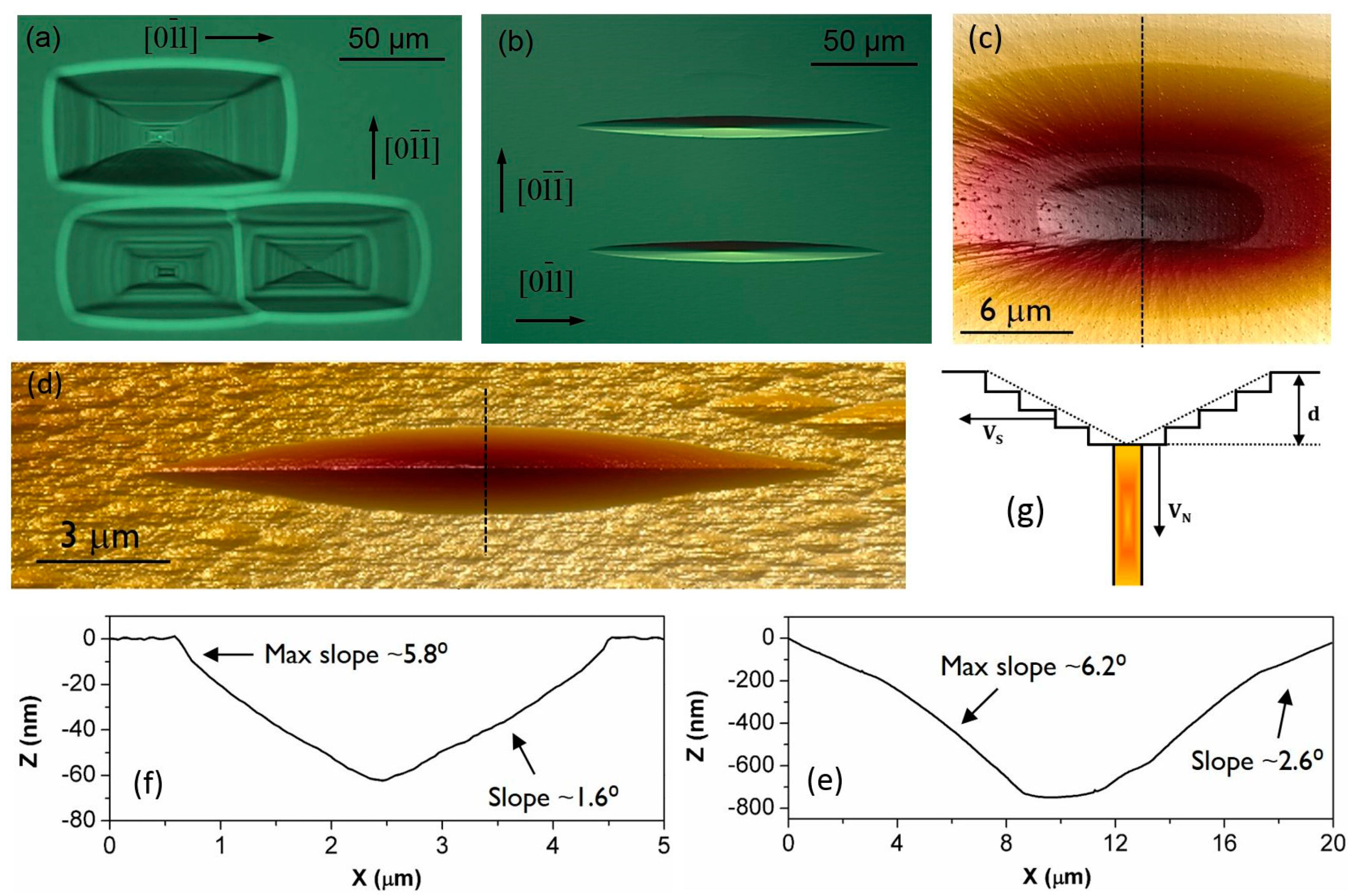
2.1. Etch Pit Formation in Bulk InP (100)

When a defect-free InP surface is etched in HBr solution through a micron-size pinhole window in a chemically-resistant mask, a rectangle-like etch pit is expected aligned along the [0 1 ¯ 1 ¯ ] and the [0 1 ¯ 1 ] directions. The elongation in the [0 1 ¯ 1 ] direction can be attributed to the higher etch rate of the (111)—P plane with respect to the (111)—In plane. Such an anisotropy in etching has been exploited during the last decades for the formation of grooves in InP, required for various optical applications [30,31]. Although (111)—In is chemically the most stable, studies have shown that other low index planes may also be revealed, depending on the chemical composition of the etchant. For instance, in HCl solution, a higher index (112) plane is observed which serves as an etch stop [32]. When extended defects are present—mainly edge-type dislocations in bulk InP (some mixed and screw dislocations may also be present) [33]—the typical anisotropy in etching is disrupted. Interruption of crystal periodicity induces a stress field and dangling bonds which lower chemical stability. The etch rate increases around the defect site and causes pit formation. Figure 1a,b shows optical microscopy images of defects revealed after a 5 min immersion in 5.9 M HBr and 5.0 M HCl solution, respectively. In the former case, rectangular etch pit features align along the [0 1 ¯ 1 ¯ ] and [0 1 ¯ 1 ] direction. The pits are more or less center symmetrical, showing that the dislocations are oriented mainly perpendicular to the surface. Etch pits can appear as pairs when two sides of a half dislocation loop are etched simultaneously. The large steps visible on the sidewalls of the pit indicate the presence of precipitants related to the Cottrell atmosphere surrounding the dislocation [34]. However, HCl immersion results in distinct boat-like pits aligned along the [0 1 ¯ 1 ] direction. No facets are present at the far ends of the pit. Figure 1c shows a tilted AFM image recorded in the center of the pit after 5 min of immersion in 5 M HBr. Although the sidewalls of the pits are quite smooth, pitting of the surface may refer to the presence of point defects.
The surface surrounding the fully imaged pit in Figure 1d (4 M HCl, 5 min immersion) shows strong roughening—critical for defect revealing in nanoscale fin structures (see the following sections). The pits obtained after etching in HBr and HCl solution are shallow, as evidenced by the small sidewall slope (see cross-section Figure 1e,f, respectively). Clearly, no (111) or (112) planes are exposed, as observed after etching defect-free bulk material. The sidewall slope is determined by the ratio of the vertical etch rate Vn at the outcrop of a dislocation and the step propagation velocity Vs (the lateral etch rate parallel to the (100) surface (Figure 1g). Although the pit depth has been correlated to the energy of dislocations (e.g., edge versus screw) [35,36], the chemical properties of the Cottrell atmosphere may also have an impact [37]. Based on inductively coupled plasma mass spectrometry measurements, we estimate that Vn is 2–3× larger than the bulk etch rate (Vb) of the (100) surface for both HBr and HCl [38]. The striking difference in pit morphology for the two acids possibly originates from an anisotropy in Vs. In earlier work, we demonstrated that the morphology of atomic terraces on InP (100) was different for H2SO4 and HCl solution, supporting such a crystal orientation dependence [38,39].
The etch pit density obtained after immersion in HBr and HCl was about 500–1000 cm−2, showing that low defect densities can be easily quantified by simple microscopy.

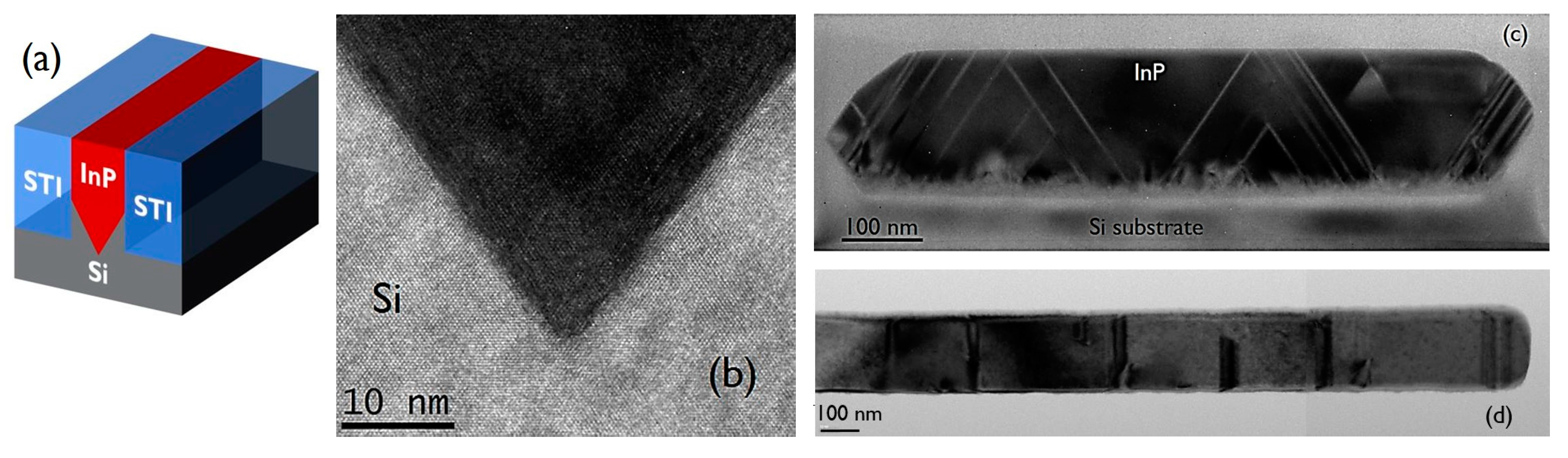
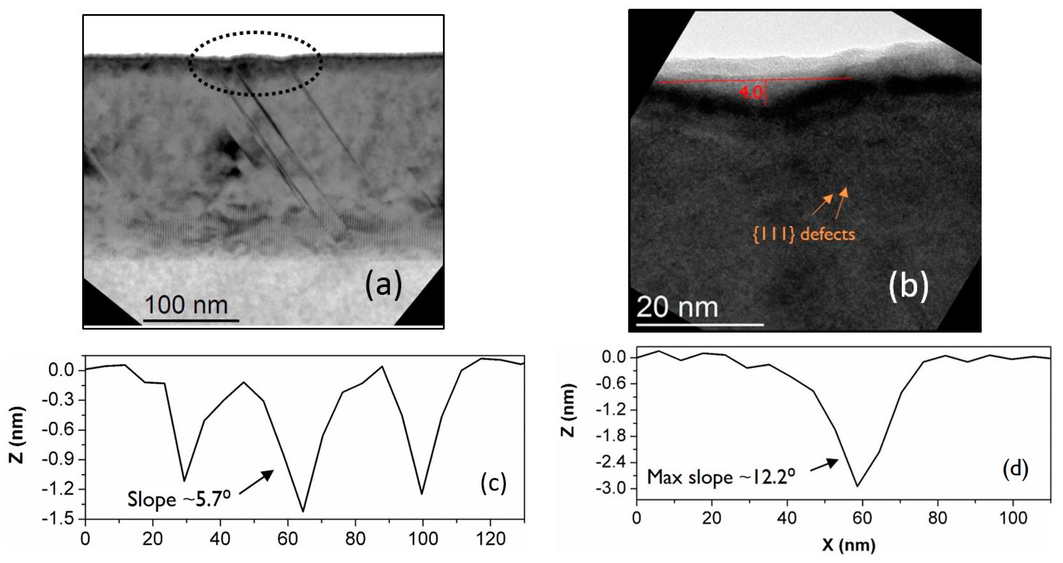
2.2. Revealing Defects in Nanoscale InP Fin Structures Grown by ART

Figure 2a shows a schematic representation of an InP fin grown on a Si V-groove inside a shallow trench isolation (STI) template, used in regular CMOS processing. The V-shaped bottom constitutes of ( 11 1 ¯ ) and ( 111 ) planes for a [0 1 ¯ 1 ] oriented trench.
A high density of stacking faults and twinning planes in the respective {111} planes are visible at the hetero-interface visualized by high-resolution TEM (HR-TEM) (Figure 2b). Although most of the defects are effectively trapped at the SiO2 sidewalls, some stacking faults and twinning planes are still able to reach the (100) fin surface in {111} planes along the fin length, clearly visible from the contrast fringes in the cross-section and plan-view TEM images (Figure 2c,d). Selective etching of such planar defects will induce grooves perpendicular to the trench along the [0 1 ¯ 1 ¯ ] direction. One important issue is that revealing stacking faults/twinning planes is impeded by fin roughening due to the highly anisotropic nature of the etchant. Furthermore, when the etch rate is too high (or the etch time too long), overlap of etched grooves from closely-spaced defects will occur. An example is shown in Figure 3a, which shows an AFM image of a 100 nm-wide fin shown after immersion in 3 M HBr for 2 min. Deep and wide grooves are visible, attributed to the presence of multiple stacking faults/twinning planes (the result for 3 M HCl is comparable.) Another complication is severe chemical attack of the (110) fin side walls (dotted arrows, Figure 3b). For this reason, we studied the fin recess (i.e., Vb) for defect-free regions relative to the unetched surface as function of HCl and HBr concentration for 40, 100, and 200 nm structures. The immersion time was kept constant at 2.5 min. For effective defect revealing, there should be minimal fin recess.
Figure 3c shows the results for a 100 nm fin. In all cases, a small but distinct difference between the acids was observed regarding the onset of etching. While the fin recess increased gradually with increasing HBr concentration, a more pronounced onset of etching was observed for HCl. Extensive AFM analysis indicated a minimum recess in the range 1.0–1.5 M HCl, providing a larger process window for defect-selective etching than HBr solution. It should be noted that the overall crystallinity and uniformity of the material across the device wafer determines the onset of etching. For instance, the etch rate of bulk (100) InP in 2 M HCl is one order of magnitude lower than that of InP fins. Any growth modification may therefore require recalibration of the acid concentration.
Figure 4a shows a top view AFM image of a 200 nm wide and 2 μm long fin section after partial STI oxide recess in 1.5% HF solution. (InP is not etched in HF: the native oxide is not fully removed by the acid). After 2.5 min of immersion in 1.25 M HCl (b), the stacking faults/twins are revealed. They cross the full width of the trench from oxide to oxide—they are not bound to dislocations. A tilted AFM image of a 1 μm fin section is shown in (c). About five to seven defects/μm length were typically detected in the 200 nm-wide fin. However, in the smaller 100 nm (d–f) and 40 nm (g–i) wide fins, the number of planar defects was larger, 10–14 defects/μm were revealed by 2.5 min of immersion in 1 M HCl solution, which is in good agreement with TEM quantification. The increase in planar defects with decreasing fin width may be attributed to a higher surface roughness of the STI walls for narrower trenches, causing additional defect nucleation during epitaxial growth. Some fin narrowing is observed after HCl immersion, attributed to anisotropy in etching—Vb (110) > (100) [27,38]. Apparently, HCl can penetrate the InP/SIO2 interface. Cross-section TEM confirms that the characteristic grooves are formed due to selective etching of {111} stacking faults and or twinning planes (Figure 5a,b). The etched grooves are fairly shallow. A typical X–Z plot obtained by AFM for a 40 nm fin (Figure 5c) shows that they are about 1 nm deep and about 20 nm wide. Defects located at a shorter range will appear as a deeper and wider feature due to overlap.
The groove shown in Figure 5d for a 100 nm fin may therefore hint to the presence of multiple surfacing defects. More dedicated TEM studies are required to further investigate this. Prolonged etching to extend the pit along the {111} plane is theoretically possible. However, deepening of the grooves in combination with increasing surface roughness (Vb ≠ 0) is not beneficial for quantification purposes.

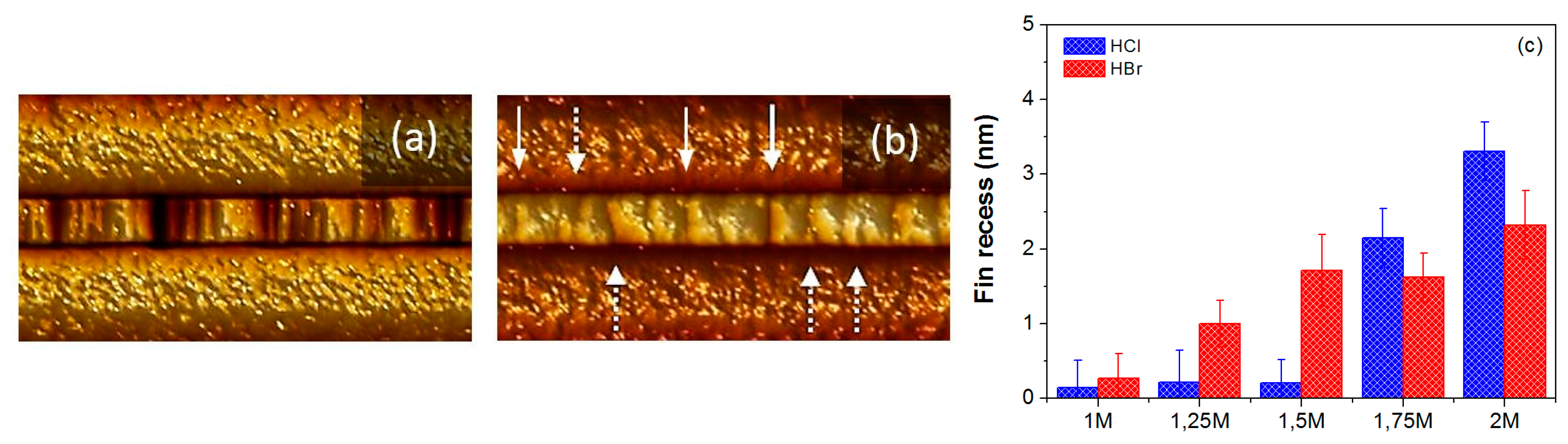
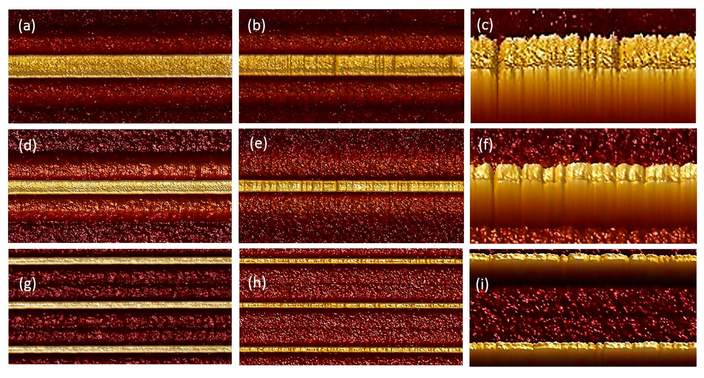
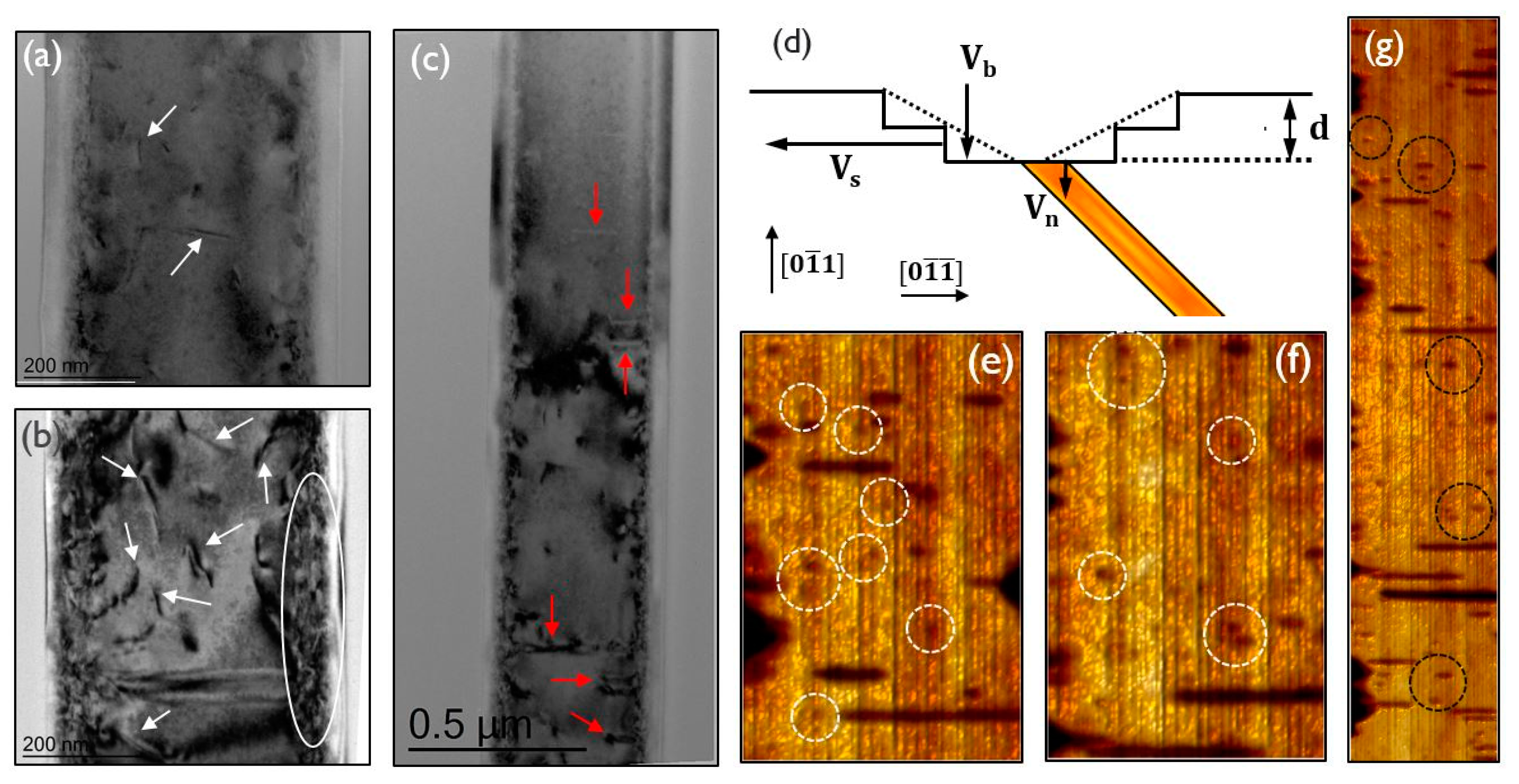
2.3. Revealing Defects in Wide-Field InP Fin Structures

Revealing defects in wide fins is more challenging. Due to ineffective ART, dislocations also reach the fin surface next to stacking faults/twinning planes (Figure 6a–c, respectively). Most dislocations run in projection on the TEM images more or less along the length of the fins. Their crossing with the surface is a point. In contrast to the observations for bulk InP (Figure 1), dislocations in InP fins are inclined as shown schematically in Figure 6d. Selective etching of the end points of these dislocations results in small and shallow pits, as indicated by the weak contrast features in the AFM images (Figure 6e,f) for 600 nm-long fin sections. The pits are only a few atomic layers deep and 10–20 nm wide. In case a dislocation is oriented perpendicular to the fin surface (as observed for bulk InP), boat-like pits would appear along the fin length (i.e., [ 0 1 ¯ 1 ] ). As the dislocations are inclined, skewed pits are expected with an asymmetry depending on the orientation of the defect. The exact shape cannot be predicted, as the Vs/Vn ratio is not necessarily constant in time due to variations in local chemical properties of the Cottrell atmosphere [37]. Obtaining pit geometry by AFM is challenging. Longer immersion times would be required to enlarge the features. This is hindered by severe attack of the fin sides, presumably by selective etching of surfacing misfit dislocations not trapped at the SiO2 sidewalls (Figure 6b,g). Increasing surface roughness with increasing etch time also lowers resolution. The process window for revealing dislocations in wide fins appears limited. Another issue is when stacking faults/twins are bound to dislocations. They appear as dark contrast lines of different lengths in AFM that do not cross the full fin width. When planar defects appear short as indicated in Figure 6g, it is hard to define “an amount of elongation” that makes the difference between stacking fault/twin and threading dislocation. AFM image analysis suggests that the former have a slightly larger contrast. More in-depth studies are needed to elucidate this.

3. Materials and Methods

Single side polished bulk (100) 2″ InP wafers with an etch pit density of −500/cm2 were obtained from AXT Inc. The n-type wafers with orientation (100) were S-doped and had a carrier concentration of 5 × 1016 cm−3.
InP fin structures were grown inside narrow trenches on V-shaped Si grooves using selective area epitaxial growth on 300 mm Si wafers [7]. The narrow trenches were made in SiO2 with fairly standard shallow trench isolation (STI) patterning technologies [40]. After growth, a chemo-mechanical polishing step was performed to remove the overgrown InP material.
Samples were etched in a cleanroom environment using standard chemicals purchased from Sigma Aldrich: 37% HCl (12.00 M) and 48% HBr (8.84 M), p.a. quality.
Etch pit features were visualized using a Zeiss Axiotron microscope set-up equipped with a CCD camera, Atomic Force Microscopy (AFM) (Bruker Dimension 3100 with Nanoscope Analysis software), and transmission electron microscopy (TEM, FEI Tecnai300F). Prior to imaging the InP fins, the fins were exposed by recessing the STI oxide by immersion in 1.5% HF solution for 2 min.

4. Conclusions

Wet-chemical defect revealing in nanoscale InP fin structures was investigated. HCl and HBr solutions were explored as defect-selective etchants using bulk InP as a reference. Pit morphology was shown to strongly depend on the acid used. Typical rectangular pits were observed for HBr solution. After immersion in HCl, boat-like features were seen. This distinct difference for the two acids is attributed to a difference in anisotropy in step edge reactivity. Center-symmetry noticed for etch pits in bulk InP suggests that the dislocations are mainly oriented perpendicular to the surface. By studying the influence of acid concentration on fin recess, it was found that HCl solution provided a larger process window for revealing defects in InP grown by the ART approach—essential for limiting surface roughening and attack of the fin side walls. Planar defects could be revealed as characteristic grooves, which was confirmed by TEM inspection. The shallow grooves were about 1 nm deep. The lowest number of stacking faults or twinning planes per unit length was observed for 200 nanometer wide trenches. A larger number was found for 40 and 100 nm-wide fins. Our data suggests that maximum one planar defect/20 nm fin length can be detected using wet-chemical etching in combination with AFM analysis. Defects at shorter range cannot be distinguished due to overlap of the etched grooves. Revealing defects is challenging in 500 nm-wide fins. Ineffective aspect ratio trapping allows dislocations to reach the surface next to stack faults and twinning planes. Due to their inclined nature, the etch pits are shallow and only a few atomic layers deep. Enlarging the pits is difficult due to the high reactivity of the fin sides and the strong surface roughening during etching. Although the process window for revealing wet-chemical defects in InP fins is small, wet-chemical etching in combination with AFM analysis has proven to be an effective and simple method for quality inspection of III-V materials relevant for N5 technology nodes and beyond.

Acknowledgments

This work is part of the IMEC Industrial Affiliation Program on Ge/III-V devices. The authors acknowledge Screen Semiconductor Solutions Co. Ltd., Entegris, ATMI, Kurita and Fuji Film Electronic Materials for their contributions to the Joint Development Program. We are grateful to Jan Weyher (Institute of High Pressure Physics, Warsaw) for the useful discussions.

Author Contributions

Sophia Arnauts etched the samples and imaged the surface by optical microscopy. AFM analysis was performed by Alain Moussa and Manuel Mannarino, the data was analyzed by Manuel Mannarino, Sophia Arnauts and Dennis Van Dorp. TEM inspection and interpretation of the results was done by Hugo Bender, Alain Moussa and Clement Merckling Fin structures were grown by Clement Merckling. Dennis Van Dorp conceived the experiments and wrote the paper together with Matty Caymax. Matty Caymax, Andreas Schulze and Wilfried Vandervorst supervised the work.

Conflicts of Interest

The authors declare no conflict of interest.

References

  1. Heyns, M.; Tsai, W. Ultimate scaling of CMOS logic devices with Ge and III–V materials. Mrs Bull. 2009, 34, 485–492. [Google Scholar] [CrossRef]
  2. Del Alamo, J.A. Nanometre-scale electronics with III–V compound semiconductors. Nature 2011, 479, 317–323. [Google Scholar] [CrossRef] [PubMed]
  3. Pillarisetty, R. Academic and industry research progress in germanium nanodevices. Nature 2011, 479, 324–328. [Google Scholar] [CrossRef]
  4. Caymax, M.; Eneman, G.; Bellenger, F.; Merckling, C.; Delabie, A.; Wang, G.; Loo, R.; Simoen, E.; Mitard, J.; Jaeger, B.D.; et al. Germanium for advanced CMOS anno 2009: A SWOT analysis. In 2009 IEEE International Electron Devices Meeting (IEDM); IEEE: Baltimore, MD, USA, 2009; pp. 1–4. [Google Scholar]
  5. Vincent, B.; Witters, L.; Richard, O.; Hikavyy, A.; Bender, H.; Loo, R.; Caymax, M.; Thean, A. Selective Growth of Strained Ge Channel on Relaxed SiGe Buffer in Shallow Trench Isolation for High Mobility Ge Planar and Fin p-FET. ECS Trans. 2013, 50, 39–45. [Google Scholar] [CrossRef]
  6. Loo, R.; Sun, J.; Witters, L.; Hikavyy, A.; Vincent, B.; Shimura, Y.; Favia, P.; Richard, O.; Bender, H.; Vandervorst, W.; et al. Strained Ge FinFET structures fabricated by selective epitaxial growth. In Proceedings of the 2014 7th International Silicon-Germanium Technology and Device Meeting (ISTDM), Singapore, 2–4 June 2014; pp. 19–20. [Google Scholar]
  7. Merckling, C.; Waldron, N.; Jiang, S.; Guo, W.; Collaert, N.; Caymax, M.; Vancoille, E.; Barla, K.; Thean, A.; Heyns, M.; et al. Heteroepitaxy of InP on Si(001) by selective-area metal organic vapor-phase epitaxy in sub-50 nm width trenches: The role of the nucleation layer and the recess engineering. J. Appl. Phys. 2014, 115, 23710. [Google Scholar] [CrossRef]
  8. Kunert, B.; Guo, W.; Mols, Y.; Tian, B.; Wang, Z.; Shi, Y.; Thourhout, D.V.; Pantouvaki, M.; Campenhout, J.V.; Langer, R.; et al. III/V nano ridge structures for optical applications on patterned 300 mm silicon substrate. Appl. Phys. Lett. 2016, 109, 91101. [Google Scholar] [CrossRef]
  9. Paladugu, M.; Merckling, C.; Loo, R.; Richard, O.; Bender, H.; Dekoster, J.; Vandervorst, W.; Caymax, M.; Heyns, M. Site Selective Integration of III–V Materials on Si for Nanoscale Logic and Photonic Devices. Cryst. Growth Des. 2012, 12, 4696–4702. [Google Scholar] [CrossRef]
  10. Mols, Y.; Kunert, B.; Gaudin, G.; Langer, R.; Caymax, M. Study towards integration of In0.53Ga0.47As on 300 mm Si for CMOS sub-7 nm node: Development of thin graded InxGa1−xAs buffers on GaAs. J. Cryst. Growth 2016, 452, 244–247. [Google Scholar] [CrossRef]
  11. Fitzgerald, E.A.; Chand, N. Epitaxial necking in GaAs grown on pre-pattemed Si substrates. J. Electron. Mater. 1991, 20, 839–853. [Google Scholar] [CrossRef]
  12. Li, J.Z.; Bai, J.; Major, C.; Carroll, M.; Lochtefeld, A.; Shellenbarger, Z. Defect reduction of GaAs/Si epitaxy by aspect ratio trapping. J. Appl. Phys. 2008, 103, 106102. [Google Scholar] [CrossRef]
  13. Krost, A.; Heinrichsdorff, F.; Bimberg, D.; Cerva, H. InP on Si(111): Accommodation of lattice mismatch and structural properties. Appl. Phys. Lett. 1994, 64, 769–771. [Google Scholar] [CrossRef]
  14. Kozlowski, G.; Fursenko, O.; Zaumseil, P.; Schroeder, T.; Vorderwestner, M.; Storck, P. (Invited) Epitaxial Growth of Low Defect SiGe Buffer Layers for Integration of New Materials on 300 mm Silicon Wafers. ECS Trans. 2013, 50, 613–621. [Google Scholar] [CrossRef]
  15. Fitzgerald, E.A.; Currie, M.T.; Samavedam, S.B.; Langdo, T.A.; Taraschi, G.; Yang, V.; Leitz, C.W.; Bulsara, M.T. Dislocations in Relaxed SiGe/Si Heterostructures. Phys. Status Solidi 1999, 171, 227–238. [Google Scholar] [CrossRef]
  16. Bedell, S.W.; Sadana, D.K.; Fogel, K.; Chen, H.; Domenicucci, A. Quick Turnaround Technique for Highlighting Defects in Thin Si/SiGe Bilayers. Electrochem. Solid State Lett. 2004, 7, G105–G107. [Google Scholar] [CrossRef]
  17. Escobedo-Cousin, E.; Olsen, S.H.; O’Neill, A.G.; Coulson, H. Defect identification in strained Si/SiGe heterolayers for device applications. J. Phys. Appl. Phys. 2009, 42, 175306. [Google Scholar] [CrossRef]
  18. Abbadie, A.; Hartmann, J.-M.; Brunier, F. A Review of Different and Promising Defect Etching Techniques: From Si to Ge. ECS Trans. 2007, 10, 3–19. [Google Scholar]
  19. Weyher, J.L.; Giling, L.J. Revealing of defects in InP by shallow (submicron) photoetching. J. Appl. Phys. 1985, 58, 219. [Google Scholar] [CrossRef]
  20. Weyher, J.; Van Enckevort, W.J.P. Selective etching and photoetching of {100} gallium arsenide in CrO3-HF aqueous solutions: II. The nature of etchFF hillocks. J. Cryst. Growth 1983, 63, 292–298. [Google Scholar] [CrossRef]
  21. Weyher, J.L.; Fornari, R.; Görög, T.; Kelly, J.J.; Erné, B. HBr-K2Cr2O7-H2O etching system for indium phosphide. J. Cryst. Growth 1994, 141, 57–67. [Google Scholar] [CrossRef]
  22. Weyher, J.L.; Kelly, J.J. Defect-Selective Etching of Semiconductors. In Springer Handbook of Crystal Growth; Dhanaraj, G., Byrappa, K., Prasad, V., Dudley, M., Eds.; Springer: Berlin/Heidelberg, Germany, 2010; pp. 1453–1476. [Google Scholar]
  23. Gerischer, H.; Mindt, W. The mechanisms of the decomposition of semiconductors by electrochemical oxidation and reduction. Electrochim. Acta 1968, 13, 1329–1341. [Google Scholar] [CrossRef]
  24. Notten, P.H.L. Etching of III-V Semiconductors: An Electrochemical Approach; Elsevier Science Ltd.: Oxford, UK; New York, NY, USA, 1992. [Google Scholar]
  25. Notten, P.H.L. The etching of InP in HCl solutions: A chemical mechanism. J. Electrochem. Soc. 1984, 131, 2641–2644. [Google Scholar] [CrossRef]
  26. Notten, P.H.L.; Damen, A.A.J.M. The electrochemistry of InP in Br2/HBr solutions and its relevance to etching behaviour. Appl. Surf. Sci. 1987, 28, 331–344. [Google Scholar] [CrossRef]
  27. Van Dorp, D.H.; Deckers, J.; Arnauts, S.; Kelly, J.J. Anisotropy in the surface chemistry of InP in acidic solutions. (In Preparation)
  28. Wang, Z.; Tian, B.; Pantouvaki, M.; Guo, W.; Absil, P.; Van Campenhout, J.; Merckling, C.; Van Thourhout, D. Room-temperature InP distributed feedback laser array directly grown on silicon. Nat. Photonics 2015, 9, 837–842. [Google Scholar] [CrossRef]
  29. Waldron, N.; Merckling, C.; Teugels, L.; Ong, P.; Ibrahim, S.A.U.; Sebaai, F.; Pourghaderi, A.; Barla, K.; Collaert, N.; Thean, A.V.-Y. InGaAs Gate-All-Around Nanowire Devices on 300 mm Si Substrates. IEEE Electron Device Lett. 2014, 35, 1097–1099. [Google Scholar] [CrossRef]
  30. Klockenbrink, R. Wet Chemical Etching of Alignment V-Grooves in (100) InP through Titanium or In[sub 0.53]Ga[sub 0.47]As Masks. J. Electrochem. Soc. 1994, 141, 1594. [Google Scholar] [CrossRef]
  31. Kuna, V.S.R.K.; Vangala, N.K.; DasGupta, A.; DasGupta, N. Effect of Etch Mask and Etching Solution on InP Micromachining to Form V-Grooves. J. Electrochem. Soc. 2001, 148, C322–C326. [Google Scholar] [CrossRef]
  32. Adachi, S. Chemical Etching Characteristics of (001) InP. J. Electrochem. Soc. 1981, 128, 1342–1349. [Google Scholar] [CrossRef]
  33. Pearsall, T.P. Properties, Processing and Applications of Indium Phosphide; Institution of Electrical Engineers: London, UK, 2000. [Google Scholar]
  34. Mahajan, S.; Moss, T.S. Handbook on Semiconductors: Materials, Properties, and Preparation; North-Holland Publishing Co.: Amsterdam, The Netherlands; New York, NY, USA, 1994. [Google Scholar]
  35. Weyher, J.L.; Lazar, S.; Macht, L.; Liliental-Weber, Z.; Molnar, R.J.; Müller, S.; Sivel, V.G.M.; Nowak, G.; Grzegory, I. Orthodox etching of HVPE-grown GaN. J. Cryst. Growth 2007, 305, 384–392. [Google Scholar] [CrossRef]
  36. Lacmann, R.K. Sangwal: Etching of crystals; theory, experiment, and application, Volume 15 aus, der Reihe: Defects in Solids, (Eds.), S. Amelinckx—J. Nihoul, North-Holland, Amsterdam, Oxford, New York, Tokyo 1987. 497 Seiten, Preis: Dfl. 275. Berichte der Bunsengesellschaft für physikalische Chemie 1987, 91, 1313. [Google Scholar] [CrossRef]
  37. Amelinckx, S. The Observation of Dislocations; Academic Press: New York, NY, USA; London, UK, 1964. [Google Scholar]
  38. Van Dorp, D.H.; Cuypers, D.; Arnauts, S.; Moussa, A.; Rodriguez, L.; De Gendt, S. Wet Chemical Etching of InP for Cleaning Applications: II. Oxide Removal. ECS J. Solid State Sci. Technol. 2013, 2, P190–P194. [Google Scholar] [CrossRef]
  39. Cuypers, D.; van Dorp, D.H.; Tallarida, M.; Brizzi, S.; Conard, T.; Rodriguez, L.N.J.; Mees, M.; Arnauts, S.; Schmeisser, D.; Adelmann, C.; et al. Study of InP Surfaces after Wet Chemical Treatments. ECS J. Solid State Sci. Technol. 2014, 3, N3016–N3022. [Google Scholar] [CrossRef]
  40. Wang, G.; Leys, M.R.; Nguyen, N.D.; Loo, R.; Brammertz, G.; Richard, O.; Bender, H.; Dekoster, J.; Meuris, M.; Heyns, M.M.; et al. Selective Area Growth of InP in Shallow-Trench-Isolated Structures on Off-Axis Si(001) Substrates. J. Electrochem. Soc. 2010, 157, H1023–H1028. [Google Scholar] [CrossRef]
Figure 1. Optical microscopy images of etch pits for bulk InP after immersion in (a) 5.9 M HBr and (b) 5.0 M HCl for 5 min. Tilted atomic force microscopy (AFM) images for etch pits obtained for (c) 5.0 M HBr and (d) 4.0 M HCl (5 min immersion). The cross-sections are shown in (e,f), respectively. A schematic representation of etch pit formation is shown in (g), reproduced by courtesy of Weyher.
Crystals 07 00098 g001
Figure 2. (a) Schematic representation of an InP fin grown on a Si V-groove in a shallow trench isolation (STI) template; (b) High-resolution TEM (HR-TEM) image recorded at the bottom of the V-groove; (c) A cross-section TEM image of a 100 nm wide and 1 μm long fin; and (d) a corresponding plan-view TEM image.
Crystals 07 00098 g002
Figure 3. Severe fin attack for 100 nm wide, 1 μm long InP fins after 2 min of etching in (a) 3 M HBr and (b) 2 M HCl solution. In each case, the SiO2 was recessed for imaging purposes. (c) Influence of acid concentration on fin recess relative to the original defect-free surface for a 100 nm-wide fin after 2.5 min of immersion.
Crystals 07 00098 g003
Figure 4. Top view AFM images of a 200 nm wide, 2 μm long fin section: (a) unetched and (b) etched for 2.5 min in 1.25 M HCl solution. (c) Side view of a 1 μm-long fin. (df) 100 nm and (gi) 40 nm wide fin sections. In these cases, the fins were immersed in 1 M HCl solution.
Crystals 07 00098 g004
Figure 5. (a,b) Cross-section TEM images of a 100 nm fin etched in 1 M HCl solution showing etched grooves on surfaced stacking faults/twins. X-Z plots recorded along the fin length by AFM for (c) a 40 nm fin and (d) a 100 nm fin after defect revealing.
Crystals 07 00098 g005
Figure 6. (a,b) Plan-view TEM images of a 500 nm-wide fin showing threading dislocations (white arrows) and misfit dislocations at the side wall. Stacking faults/twinning planes are indicated by the red arrows in (c). (d) Schematic representation of an inclined threading dislocation below a formed etch pit. (e,f) AFM images of 600 nm-long fin sections indicating dislocation pits revealed by immersion in 1.25 M HCl. (g) A 2 μm long fin section. The indicated pits may be stacking faults/twins or threading dislocations.
Crystals 07 00098 g006

