
Synthesis and Thermoelectric Properties of Copper Sulfides via Solution Phase Methods and Spark Plasma Sintering

Faculty of Materials Science and Engineering, Kunming University of Science and Technology, Kunming 650093, China
*
Author to whom correspondence should be addressed.
Crystals 2017, 7(5), 141; https://doi.org/10.3390/cryst7050141
Submission received: 27 April 2017
/
Revised: 12 May 2017
/
Accepted: 13 May 2017
/
Published: 16 May 2017
(This article belongs to the Special Issue Materials Processing and Crystal Growth for Thermoelectrics)
Abstract
:Large-scale Cu2S tetradecahedrons microcrystals and sheet-like Cu2S nanocrystals were synthesized by employing a hydrothermal synthesis (HS) method and wet chemistry method (WCM), respectively. The morphology of α-Cu2S powders prepared by the HS method is a tetradecahedron with the size of 1–7 μm. The morphology of β-Cu2S is a hexagonal sheet-like structure with a thickness of 5–20 nm. The results indicate that the morphologies and phase structures of Cu2S are highly dependent on the reaction temperature and time, even though the precursors are the exact same. The polycrystalline copper sulfides bulk materials were obtained by densifying the as-prepared powders using the spark plasma sintering (SPS) technique. The electrical and thermal transport properties of all bulk samples were measured from 323 K to 773 K. The pure Cu2S bulk samples sintered by using the powders prepared via HS reached the highest thermoelectric figure of merit (ZT) value of 0.38 at 573 K. The main phase of the bulk sample sintered by using the powder prepared via WCM changed from β-Cu2S to Cu1.8S after sintering due to the instability of β-Cu2S during the sintering process. The Cu1.8S bulk sample with a Cu1.96S impurity achieved the highest ZT value of 0.62 at 773 K.

1. Introduction
Thermoelectric (TE) material is a kind of energy conversion material which takes advantage of solid material internal carriers and phonon interactions to convert thermal and electrical energy directly into each other. The energy crisis and environmental problems have promoted the swift development of TE materials in the past few decades [1,2,3,4]. Compared to the mainstream tellurium-based TE materials [5,6,7,8], nanostructured metal chalcogenides with low cost, low toxicity, and abundant elements exhibit interesting physical properties [9,10]. Therefore, nanostructured metal chalcogenides TE materials such as Cu-Se [11,12,13] and Cu-S materials [14,15,16,17] have received more attention.
Copper sulfides (Cu2 − xS (0 ≤ x ≤ 1)), with different copper stoichiometric ratios, which are a series of compounds ranging from copper-rich Cu2S to copper deficient CuS, are considered to be superionic conductors [18]. As an important semiconductor, Cu2S is of high interest due to its unique electronic, thermodynamic, optical, and other physical and chemical properties. It has great potential in a wide range of applications such as thermoelectric materials [19], solar cells [20,21], conductive fibers [22], optical filters [23], and high-capacity cathode materials in lithium secondary batteries [24]. Moreover, Cu2S nanoparticles with various morphologies have been synthesized by various approaches such as chemical precipitation [25], solventless thermolysis [26], water-oil interface confined method [27], and thermal decomposition [28].
Here, we employed facile solution methods, including hydrothermal synthesis (HS) and wet chemistry method (WCM), to synthesize Cu2S powders with controllable microstructures under relatively facile conditions. Then, polycrystalline copper sulfides were fabricated by densifying the compound powders using the spark plasma sintering (SPS) technique. The thermoelectric properties of all the bulk samples were measured.
2. Experimental Section
Commercial high-purity powders of CuO (99.9%) and S (99.99%) were used as raw materials. Meanwhile, ethylene diamine (EDA) and hydrazine hydrate (N2H4·H2O) were used as a chelating agent (EDA) and a reducing agent (N2H4·H2O), respectively. In a typical wet chemistry method, CuO (10 mmol) and S (20 mmol) were first added to EDA (40 mL) by stirring at room temperature for 10 min. Then, N2H4·H2O (35 mL) was dripped slowly into the beaker under further stirring for 12 h at room temperature. The chelating agent EDA reacted with Cu ions to form the complex compounds for avoiding the precipitation of metal Cu. The reducing agent N2H4·H2O reduced the Cu2+ to Cu+ and S to S2−, respectively.
In a typical hydrothermal synthesis [29] method, CuO (10 mmol) and S (20 mmol) were first added to EDA (40 mL), and the mixture was stirred and heated to 373 K for 10 min. After that, N2H4·H2O (35 mL) was dripped slowly into the solution under further stirring for 10 min at 373 K. The mixed solution was then transferred into a Teflon-lined stainless steel autoclave (100 mL capacity), which was sealed and maintained at 453 K for 6 h. The final solid products were filtered and washed with DI water and ethanol three times before drying under vacuum at 333 K for 12 h.
The resultant powders were loaded into a graphite die with an inner diameter of 15 mm and then sintered at 773 K for 5 min (heating rate of 100 K/min) under an axial compressive stress of 40 MPa in a vacuum by using a spark plasma sintering (SPS) system (SPS1050; Sumitomo, Tokyo, Japan). The SPS-prepared specimens were disk-shaped with dimensions of Ф15 mm × 4 mm. The phase structure was analyzed by X-ray diffraction with a Cu Kα radiation (λ = 1.5406 Å) filtered through Ni foil (RAD-B system; Rigaku, Tokyo, Japan). The morphologies of the powders and the fracture of the bulk samples were observed by field-emission scanning electron microscopy (FESEM, SUPRA 55, Carl Zeiss, Oberkochen, Germany). The microstructure of the powder was also checked using transmission electron microscopy (TEM, Phililp Tecnai F20, Amsterdam, Dutch). In a typical TEM sample preparation procedure, powders were first added to ethyl alcohol, and stirred for 10 min by ultrasound. Then, the supernatant was dropped on the copper grid.
The electrical transport properties were evaluated along a sample section perpendicular to the SPS pressing direction. The Seebeck coefficient and electrical resistivity were measured from 323 to 773 K in a helium atmosphere using a Seebeck coefficient/electrical resistance measuring system (ZEM-3, Ulvac-Riko, Kanagawa, Japan). The density (d) of the sample was measured by the Archimedes method. In addition, the thermal conductivity of the samples was calculated by the relationship κ = DCpd from the thermal diffusivity D measured by the laser flash method (LFA457; NETZSCH, Selb, Bavaria, Germany).
3. Results and Discussion
3.1. Powder Synthesis and Characterization
3.1.1. XRD Analysis
Figure 1 shows the XRD patterns of Cu2S powders which prepared by WCM and HS methods. All of the diffraction peaks of the HS sample are well-matched with the standard card of α-Cu2S (JSPDS no. 83-1462), showing that the pure monoclinic α-Cu2S powders were obtained by HS methods. All of the diffraction peaks of the WCM sample are well-matched with the standard card β-Cu2S (JCPDS no. 26-1116), showing that the pure hexagonal β-Cu2S powders were obtained by WCM. Actually, the hexagonal β-Cu2S is high-chalcocite (378–698 K); it would be not stable under thermal shock. The diffraction peaks of powder samples are wider compared to the standard card, indicating the small grain size of the obtained powder. The XRD refinement was performed for the two samples as shown in Figures S1 and S2. The location, proportion and lattice constant of experiment and refinement Cu ions for hexagonal β-Cu2S powder are shown in Table S1. The proportion of Cu1 changed from 0.75 to 0.4896, indicating that there are more Cu vacancies, smaller lattice parameters, and the possibility of defects in hexagonal Cu2S.
3.1.2. FESEM and TEM Analysis
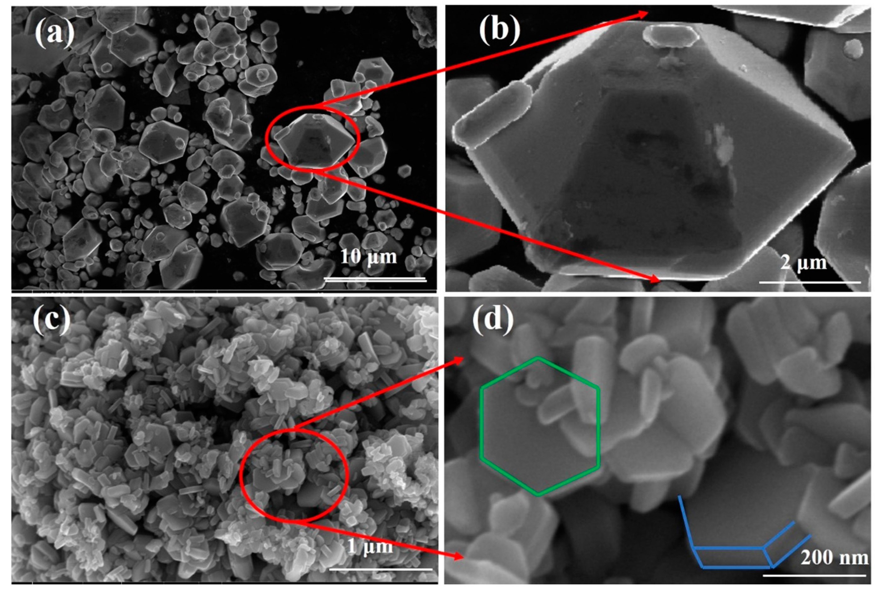
Figure 2 shows the FESEM images of Cu2S prepared by different synthesis methods. The pure α-Cu2S powder which was prepared by the HS method is shown in Figure 2a. The morphology of α-Cu2S powder prepared by the HS method is a tetradecahedron with the size of 1–7 μm. Figure 2b is a magnified image of a typical single-crystalline α-Cu2S, shown in Figure 2a. The pure β-Cu2S powder which was prepared by WCM is shown in Figure 2c. The morphology of hexagonal β-Cu2S is hexagonal nanosheets. Each nanosheet has an edge length of 10–200 nm and a thickness of 5–20 nm. The morphologies of the powder are highly related to the crystal structure [30]. Similar work reported in the literature for molybdate materials [31] suggests that the synthesis temperature has a strong influence on the morphology of Cu2S samples. Under the synthesis conditions of high temperature and high pressure, the monoclinic α-Cu2S showed a tetradecahedron morphology. Also, under relatively mild synthesis conditions (WCM), the hexagonal β-Cu2S nanosheets were synthesized at room temperature.
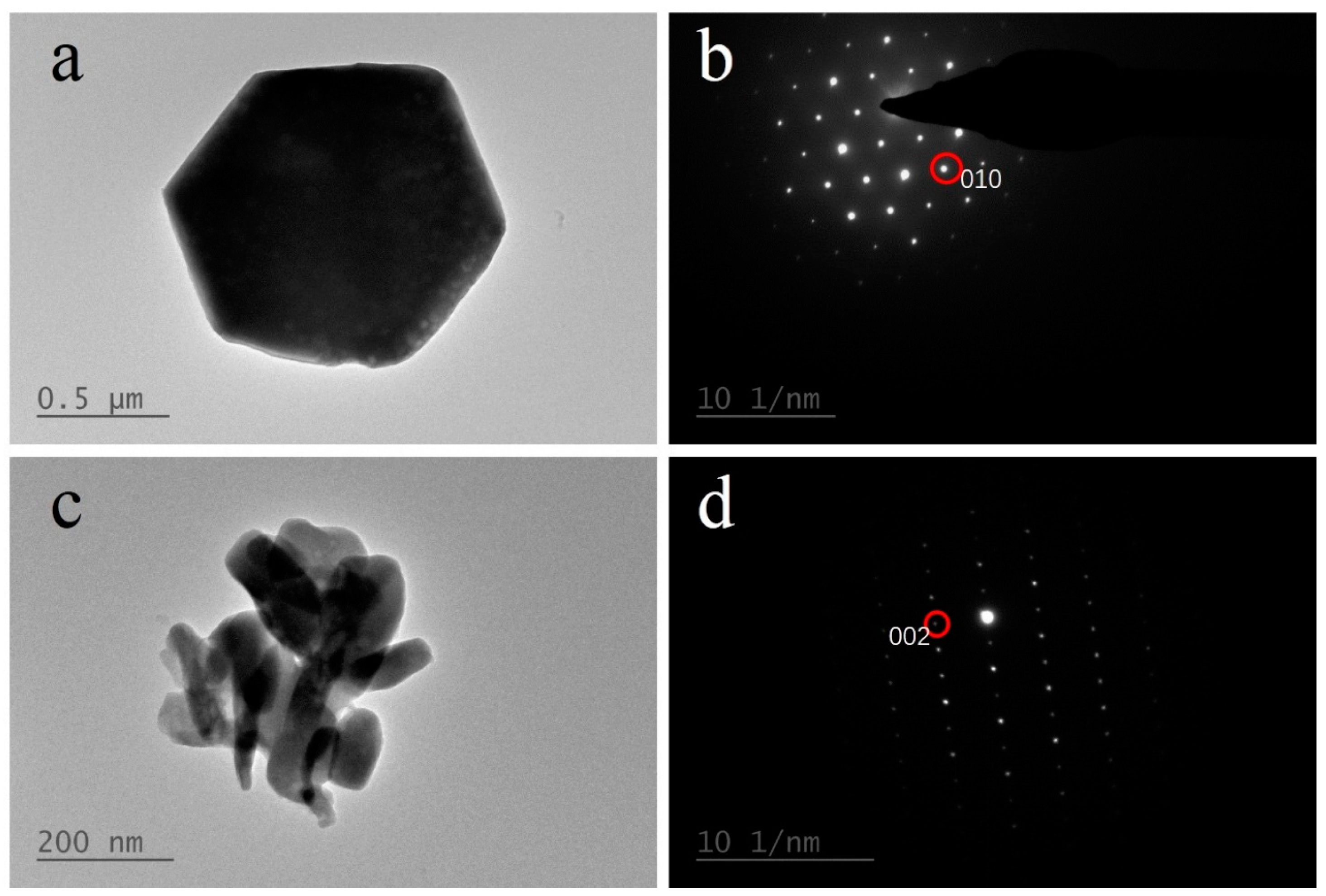
The high magnification FEM image of β-Cu2S is shown in Figure 2d. The β-Cu2S has a hexagonal sheet-like structure with a thickness of 20 nm. The TEM image (Figure 3a) and selected area of electron diffraction (SAED) patterns (Figure 3b) of a single crystal α-Cu2S revealed a tetradecahedron Cu2S of 1 μm in width. The SAED pattern for the tetradecahedron particles (Figure 2b) indicated a highly crystallized monoclinic structure of the α-Cu2S. Additionally, the TEM image (Figure 3c) and SAED patterns (Figure 3d) of a single-crystalline β-Cu2S revealed a sheet-like Cu2S of 10–200 nm in width and of 5–20 nm in thickness. The results are in agreement with SEM observations.
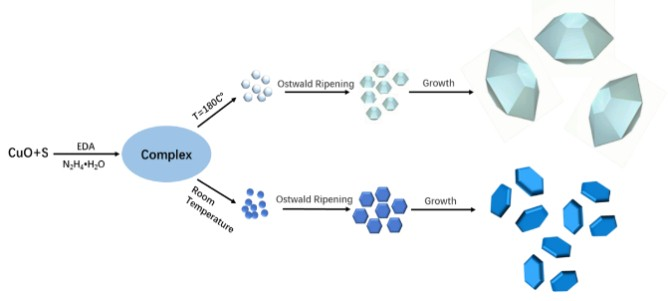
3.1.3. Synthesis Mechanism
The synthesis process and mechanism of Cu2S, similar to the flower-like α-Fe2O3 reported by Penki et al. [32], were investigated in detail, as shown in Figure 4. The raw CuO (black) and S (yellow) were mixed in a N2H4·H2O and EDA solution to initially produce the precursor Cu2O and S2−, and then further react to become the product Cu2S under the different reaction conditions. When the HS method was employed, the reaction temperature was 453 K and the product was monoclinic α-Cu2S, as indicated in XRD shown in Figure 1. After 6 h of hydrothermal reaction, the single crystal monoclinic α-Cu2S formed a tetradecahedron with a dimension of several micrometers as shown in Figure 2a. But when WCM was employed with a reaction temperature of room temperature, the product was hexagonal β-Cu2S, as indicated in XRD shown in Figure 1. After a 12-h reaction, the single crystal hexagonal β-Cu2S grew to form nanosheets with an edge length of 10–200 nm and thickness of 5–20 nm as shown in Figure 2c. The reaction process can be described by Equations (1)–(3).
2CuO + 2N2H4·H2O → Cu2O + 2NH4+ + H2O + 2OH− + N2↑
S + 2N2H4·H2O → S2− + 2NH4+ + 2H2O + N2↑
2Cu2O + 2S2− + 2H2O → 2Cu2S + 4OH-
Finally, it is suggested that the morphologies and phase structures of Cu2S are highly dependent on the reaction temperature and time, even if precursors are exactly the same.
3.2. Bulk Characterization
3.2.1. XRD and FESEM Analysis
The bulk sample abbreviated as HS-bulk was prepared by applying SPS at 773 K for 5 min using monoclinic α-Cu2S powders. The bulk sample abbreviated as WCM-bulk was prepared by applying SPS at 773 K for 5 min using hexagonal β-Cu2S powders. The XRD patterns of those bulk samples are shown in Figure 5a. The green arrows index the impurity peaks of Cu1.96S. The HS-bulk is still in the α-Cu2S phase. The SEM image of HS-bulk shown in Figure 5b shows a high relative density of 96% and an average grain size of 5 μm, which is very similar to the powders formed by the rapid sintering process. SPS is a rapid sintering technology, after which the nanoscale particles can be maintained in bulk [14]. As shown in the XRD pattern (Figure 5a), the WCM-bulk exhibits a main phase of Cu1.8S with an impurity of Cu1.96S. The hexagonal β-Cu2S is in the high-chalcocite phase, which is instable during the sintering process. Because of thermal shock in the SPS process, the phase transition occurred from β-Cu2S to Cu1.8S, which is the most stable phase in the Cu-S system. Cu2S is a superionic conductor, and the superionic phase transition temperature is over 689 K [33]. In the SPS sintering program, the sintering temperature is 773 K, and the Cu ions show liquid behavior under this temperature. The extra Cu may precipitate on the anode and be removed during the polishing and cutting process. As shown in Figure 5c, the WCM-bulk sample with a relative density of 90.2% has an average size of 200 nm.
3.2.2. Thermoelectric Transport Properties
The TE properties of the two bulk samples were measured. The TE properties of Cu1.8S bulk sample in the literature [34], which were prepared by the same SPS process but using the mechanical alloying (MA) treated powders, are shown for comparison. Figure 6a illustrates the temperature dependence of electrical conductivity (σ) for the bulk samples. As shown in Figure 6a, the HS-bulk has the highest σ value up to 218 Scm−1 at 373 K, and WCM-bulk has the highest σ value up to 2490 Scm−1 at 373 K. Both the HS-bulk and the WCM-bulk have lower σ than the MA-bulk. The WCM-bulk has a similar main phase to the MA-bulk but a low relative density and impurity of Cu1.96S, which decrease the σ value. The HS-bulk sample has the main phase of Cu2S, while the electrical conductivity of Cu2−xS depends on the Cu content due to its superionic behavior. Therefore, the HS-bulk sample has the lowest electrical conductivity. The WCM-bulk sample has one turning point in the σ curve due to the one phase transition of Cu1.8S during the measured temperature range of 323 K to 773 K [34]. Two turning points in the σ curve were observed for the HS-bulk sample due to the two phase transitions of Cu2S during the measured temperature range. As reported by Li et al., bulk Cu2S exhibits three phases (α-phase, β-phase, γ-phase) in the temperature ranges of >698, 378–698, and <378 K [35,36], respectively. The high temperature region to the right of the blue dashed line in Figure 6 and Figure 7 is the γ-phase.
The positive Seebeck coefficient (α) in Figure 6b indicates all bulks are p-type semiconductors. According to the equations σ = eμn, and α ≈ γ − lnn, [37] where σ, μ, n, α and γ are electrical conductivity, carrier mobility, carrier concentration, Seebeck coefficient and scattering factor, respectively, α is usually inversely proportional to σ. The HS-bulk achieved the largest α value of 532 μVK−1 at 673 K. The WCM-bulk achieved the largest α value of 101 μVK−1 at 773 K. The PF was calculated by PF = α2σ and is shown in Figure 6c. The PF of the HS-bulk reaches 196 μWm−1K−2 at 573 K, and that of the WCM-bulk achieved 985 μWm−1K−2 at 773 K.
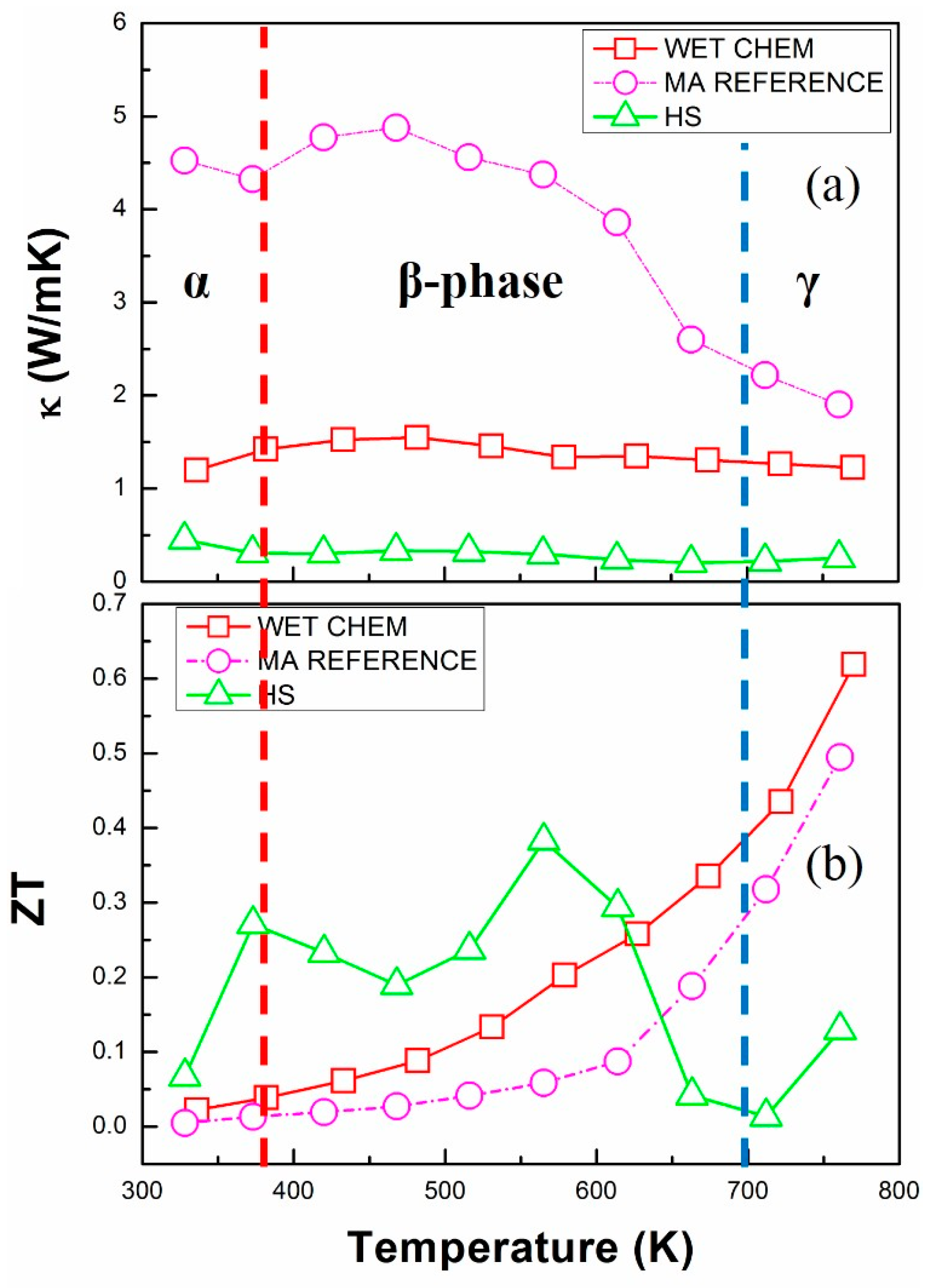
Figure 7 shows the temperature dependence of thermal conductivity (κ) (a) and the thermoelectric figure of merit, ZT (b). The κ value of the HS-bulk and the WCM-bulk are lower than that of the MA-bulk [34], due to the fine grain size and the lower relative density. The HS-bulk sample obtained the lowest κ value of 0.20 WmK−1 at 673 K. The WCM-bulk sample obtained the lowest κ value of 1.23 WmK−1 at 773 K. The κ curve of the HS sample also has two turning points according to the two phases transitions of Cu2S, which are also similar to the previous report by He et al. [33]. Based on the above measurement results, the ZT was calculated by ZT = σα2 T/κ as shown in Figure 7b. The highest ZT value of 0.38 was obtained at 573 K for the HS-bulk sample, and the WCM-bulk sample obtained the highest ZT value of 0.62 at 773 K. This shows that Cu2S is a promising thermoelectric material, and the method combining the solution phase method and SPS may be an efficient route for synthesizing high performance bulk TE materials [37].
4. Conclusions
The stable solution phase processes for preparing the single phase Cu2S powders were obtained. Large-scale Cu2S tetradecahedron microcrystals with monoclinic symmetry and sheet-like Cu2S nanocrystals with hexagonal β-Cu2S symmetry were synthesized by employing the hydrothermal synthesis (HS) method and the wet chemistry method (WCM), respectively. The Cu2S nanopowders were densified to bulk by SPS. Due to the fine grains, low thermal conductivity was achieved, resulting in enhanced TE properties. The highest ZT value of 0.38 was obtained at 573 K for the HS-bulk sample, which is better than the values achieved by the other two samples in this temperature. The WCM-bulk sample obtained the highest ZT value of 0.62 at 773 K. Compared with the MA-bulk [34], the WCM-bulk has a 26.53% increase of ZT value at 773 K. Our work indicated that the morphologies and phase structures of Cu2S are highly dependent on the reaction temperature and time even when the raw materials were exactly the same.
Supplementary Materials
The following are available online at https://www.mdpi.com/2073-4352/7/5/141/s1, Figure S1: XRD refinement patterns of the hexagonal Cu2S powder sample, Figure S2: XRD refinement patterns of the monoclinic Cu2S powder sample, Table S1: The location, proportion and lattice constant of Cu ions, Table S2: The lattice constant of monoclinic Cu2S powder sample.
Acknowledgments
This work was supported by the National Natural Science Foundation of China (Grant No. 51501086).
Author Contributions
All authors participated in the research, analysis and writing of the manuscript. Zhen-Hua Ge designed the experiments and Yun-Qiao Tang fabricated the samples, preformed the thermoelectric properties characterization and wrote the paper.
Conflicts of Interest
The authors declare no conflicts of interest.
References
- Sales, B.C. Smaller is cooler. Science 2001, 295, 1248–1249. [Google Scholar] [CrossRef] [PubMed]
- Sootsman, J.R.; Chung, D.Y.; Kanatzidis, M.G. New and old concepts in thermoelectric materials. Angew. Chem. Int. Ed. 2009, 48, 8616–8639. [Google Scholar] [CrossRef] [PubMed]
- Snyder, G.J.; Eric, S.T. Complex thermoelectric materials. Nat. Mater. 2008, 7, 105–114. [Google Scholar] [CrossRef] [PubMed]
- Di Salvo, F.J. Thermoelectric Cooling and Power Generation. Science 1999, 285, 703–706. [Google Scholar] [CrossRef]
- Zhao, X.B.; Ji, X.H.; Zhang, Y.H.; Zhu, T.J.; Tu, J.P.; Zhang, X.B. Bismuth telluride nanotubes and the effects on the thermoelectric properties of nanotube-containing nanocomposites. Appl. Phys. Lett. 2005, 86, 062111. [Google Scholar] [CrossRef]
- Zhang, Y.C.; Wang, H.; Kraemer, S.; Shi, Y.F.; Zhang, F.; Snedaker, M.; Ding, K.; Moskovits, M.; Snyder, G.J.; Stucky, G.D. Surfactant-Free Synthesis of Bi2Te3-Te Micro-Nano Heterostructure with Enhanced Thermoelectric Figure of Merit. ACS Nano 2011, 5, 3158–3165. [Google Scholar] [CrossRef] [PubMed]
- Heremans, J.P.; Jovovic, V.; Toberer, E.S.; Saramat, A.; Kurosaki, K.; Charoenphakdee, A.; Yamanaka, S.; Snyder, G.J. Enhancement of thermoelectric efficiency in PbTe by distortion of the electronic density of states. Science 2008, 321, 554–557. [Google Scholar] [CrossRef] [PubMed]
- Li, Z.Y.; Li, J.F.; Zhao, W.Y.; Tan, Q.; Wei, T.R.; Wu, C.F.; Xing, Z.B. PbTe-based thermoelectric nanocomposites with reduced thermal conductivity by SiC nanodispersion. Appl. Phys. Lett. 2014, 104, 113905. [Google Scholar] [CrossRef]
- Gao, M.R.; Xu, Y.F.; Jiang, J.; Yu, S.H. Nanostructured metal chalcogenides: Synthesis, modification, and applications in energy conversion and storage devices. Chem. Soc. Rev. 2013, 42, 2986–3017. [Google Scholar] [CrossRef] [PubMed]
- Ge, Z.H.; Nolas, G.S. Controllable Synthesis of Bismuth Chalcogenide Core–shell Nanorods. Cryst. Growth Des. 2014, 14, 533–536. [Google Scholar] [CrossRef]
- Liu, H.L.; Shi, X.; Xu, F.F.; Zhang, L.L.; Zhang, W.Q.; Chen, L.D.; Uher, C.; Day, T.; Snyder, G.J. Copper ion liquid-like thermoelectrics. Nat. Mater. 2012, 11, 422–425. [Google Scholar] [CrossRef] [PubMed]
- Li, D.; Qin, X.Y.; Liu, Y.F.; Song, C.J.; Wang, L.; Zhang, J.; Xin, H.X.; Guo, G.L.; Zou, T.H.; Sun, G.L.; et al. Chemical synthesis of nanostructured Cu2Se with high thermoelectric performance. RSC Adv. 2014, 4, 8638–8644. [Google Scholar] [CrossRef]
- Shi, X.; Xi, L.; Fan, J.; Zhang, W.; Chen, L. Cu-Se bond network and thermoelectric compounds with complex diamondlike structure. Chem. Mater. 2010, 22, 6029–6031. [Google Scholar] [CrossRef]
- Ge, Z.H.; Zhang, B.P.; Chen, Y.X.; Yu, Z.X.; Liu, Y.; Li, J.F. Synthesis and transport property of Cu1.8S as a promising thermoelectric compound. Chem. Commun. 2011, 47, 12697–12699. [Google Scholar] [CrossRef] [PubMed]
- Dennler, G.; Chmielowski, R.; Jacob, S.; Capet, F.; Roussel, P.; Zastrow, S.; Nielsch, K.; Opahle, I.; Madsen, G.K.H. Are binary copper sulfides/selenides really new and promising thermoelectric materials? Adv. Energy Mater. 2014, 4, 1301581. [Google Scholar] [CrossRef]
- Abdullaev, G.B.; Aliyarova, Z.A.; Zamanova, E.H.; Asadov, G.A. Investigation of the electric properties of Cu2S single crystals. Phys. Status Solidi 1968, 26, 65–68. [Google Scholar] [CrossRef]
- Lu, X.; Morelli, D.T.; Xia, Y.; Zhou, F.; Ozolins, V.; Chi, H.; Zhou, X.Y.; Uher, C. High Performance Thermoelectricity in Earth-Abundant Compounds Based on Natural Mineral Tetrahedrites. Adv. Energy Mater. 2013, 3, 342–348. [Google Scholar] [CrossRef]
- Miller, T.A.; Wittenberg, J.S.; Wen, H.; Connor, S.; Cui, Y.; Lindenberg, A.M. The mechanism of ultrafast structural switching in superionic copper (I) sulphide nanocrystals. Nat. Commun. 2013, 4, 1369. [Google Scholar] [CrossRef] [PubMed]
- El Akkad, F.; Mansour, B.; Hendeya, T. Electrical and thermoelectric properties of Cu2Se and Cu2S. Mater. Res. Bull. 1981, 16, 535–539. [Google Scholar] [CrossRef]
- Rothwarf, A. The CdS/Cu2S solar cell: Basic operation and anomalous effects. Sol. Cells 1980, 2, 115–140. [Google Scholar] [CrossRef]
- Hall, R.B.; Meakin, J.D. The design and fabrication of high efficiency thin film CdS/Cu2S solar cells. Thin Solid Films 1979, 63, 203–211. [Google Scholar] [CrossRef]
- Kim, S.; Kim, S.; Kim, Y.H.; Ku, B.C.; Jeong, Y. Enhancement of electrical conductivity of carbon nanotube fibers by copper sulfide plating. Fibers Polym. 2015, 16, 769–773. [Google Scholar] [CrossRef]
- Fernandez, A.M.; Nair, M.T.S.; Nair, P.K. Chemically deposited ZnS-NiS-CuS optical filters with wide range solar control characteristics. Mater. Manuf. Process 1993, 8, 535–548. [Google Scholar] [CrossRef]
- Lai, C.H.; Huang, K.W.; Cheng, J.H.; Lee, C.Y.; Hwang, B.J.; Chen, L.J. Direct growth of high-rate capability and high capacity copper sulfide nanowire array cathodes for lithium-ion batteries. J. Mater. Chem. 2010, 20, 6638–6645. [Google Scholar] [CrossRef]
- Wu, S.X.; Jiang, J.; Liang, Y.G.; Yang, P.; Niu, Y.; Chen, Y.D.; Xia, J.F.; Wang, C. Chemical Precipitation Synthesis and Thermoelectric Properties of Copper Sulfide. J. Electron. Mater. 2017, 46, 2432–2437. [Google Scholar] [CrossRef]
- Sigman, M.B.; Ghezelbash, A.; Hanrath, T.; Saunders, A.E.; Lee, F.; Korgel, B.A. Solventless synthesis of monodisperse Cu2S nanorods, nanodisks, and nanoplatelets. J. Am. Chem. Soc. 2003, 125, 16050–16057. [Google Scholar] [CrossRef] [PubMed]
- Zhuang, Z.B.; Peng, Q.; Zhang, B.; Li, Y.D. Controllable synthesis of Cu2S nanocrystals and their assembly into a superlattice. J. Am. Chem. Soc. 2008, 130, 10482–10483. [Google Scholar] [CrossRef] [PubMed]
- Liu, Z.P.; Xu, D.; Liang, J.B.; Shen, J.M.; Zhang, S.Y.; Qian, Y.T. Growth of Cu2S ultrathin nanowires in a binary surfactant solvent. J. Phys. Chem. 2005, 109, 10699–10704. [Google Scholar] [CrossRef] [PubMed]
- Yin, C.Y.; Minakshi, M.; Ralph, D.E.; Jiang, Z.T.; Xie, Z.H.; Guo, H. Hydrothermal synthesis of cubic α-fe2O3, microparticles using glycine: Surface characterization, reaction mechanism and electrochemical activity. J. Alloys Compd. 2011, 509, 9821–9825. [Google Scholar] [CrossRef]
- Zhang, Y.Q.; Zhang, B.P.; Ge, Z.H.; Zhu, L.F.; Li, Y. Preparation by solvothermal synthesis, growth mechanism, and photocatalytic performance of CuS nanopowders. Eur. J. Inorg. Chem. 2014, 2014, 2368–2375. [Google Scholar] [CrossRef]
- Barmi, M.J.; Minakshi, M. Tuning the redox properties of the nanostructured CoMoO4 electrode: Effects of surfactant content and synthesis temperature. ChemPlusChem 2016, 81, 964–977. [Google Scholar] [CrossRef]
- Penki, T.R.; Shivakumara, S.; Minakshi, M.; Munichandraiah, N. Porous Flower-like α-Fe2O3 Nanostructure: A High Performance Anode Material for Lithium-ion Batteries. Electrochim. Acta 2015, 167, 330–339. [Google Scholar] [CrossRef]
- He, Y.; Day, T.; Zhang, T.S.; Liu, H.L.; Shi, X.; Chen, L.D.; Snyder, G.J. High Thermoelectric Performance in Non-Toxic Earth-Abundant Copper Sulfide. Adv. Mater. 2014, 26, 3974–3978. [Google Scholar] [CrossRef] [PubMed]
- Ge, Z.H.; Liu, X.Y.; Feng, D.; Lin, J.Y.; He, J.Q. High-Performance Thermoelectricity in Nanostructured Earth-Abundant Copper Sulfides Bulk Materials. Adv. Energy Mater. 2016, 6, 1600607. [Google Scholar] [CrossRef]
- Li, B.; Huang, L.; Zhao, G.Y.; Wei, Z.M.; Dong, H.L.; Hu, W.P.; Wang, L.W.; Li, J.B. Large-Size 2D β-Cu2S Nanosheets with Giant Phase Transition Temperature Lowering (120 K) Synthesized by a Novel Method of Super-Cooling Chemical-Vapor-Deposition. Adv. Mater. 2016, 28, 8271–8276. [Google Scholar] [CrossRef] [PubMed]
- Okamoto, K.; Kawai, S. Electrical conduction and phase transition of copper sulfides. Jpn. J. Appl. Phys. 1973, 12, 1130. [Google Scholar] [CrossRef]
- Ge, Z.H.; Zhao, L.D.; Wu, D.; Zhang, B.P.; Li, J.F.; He, J.Q. Low cost, abundant binary sulfides as promising thermoelectric. Mater. Today 2016, 19, 227–239. [Google Scholar] [CrossRef]
Figure 1.
XRD patterns with a selected 2θ range of 20°–70° for Cu2S powders.

Figure 2.
Field emission scanning electron microscopy patterns of the powders under different magnifications. (a,b) Cu2S powders prepared by HS; (c,d) Cu2S powders prepared by WCM.
Figure 2.
Field emission scanning electron microscopy patterns of the powders under different magnifications. (a,b) Cu2S powders prepared by HS; (c,d) Cu2S powders prepared by WCM.

Figure 3.
TEM image and SAED patterns for HS-Cu2S powder (a,c) and WCM-Cu2S powder (b,d).

Figure 4.
Schematic illustration of the growth mechanism of the Cu2S powders synthesized by the WCM and HS methods.
Figure 4.
Schematic illustration of the growth mechanism of the Cu2S powders synthesized by the WCM and HS methods.

Figure 5.
XRD patterns with a selected 2θ range of 20°–70° for bulk samples prepared by SPS at 773 K for 5 min, and field emission scanning electron microscopy of the fractured surfaces for the bulk samples. (a) XRD patterns of the two bulk samples; (b) FESEM image of HS-bulk; (c) FESEM image of WCM-bulk.
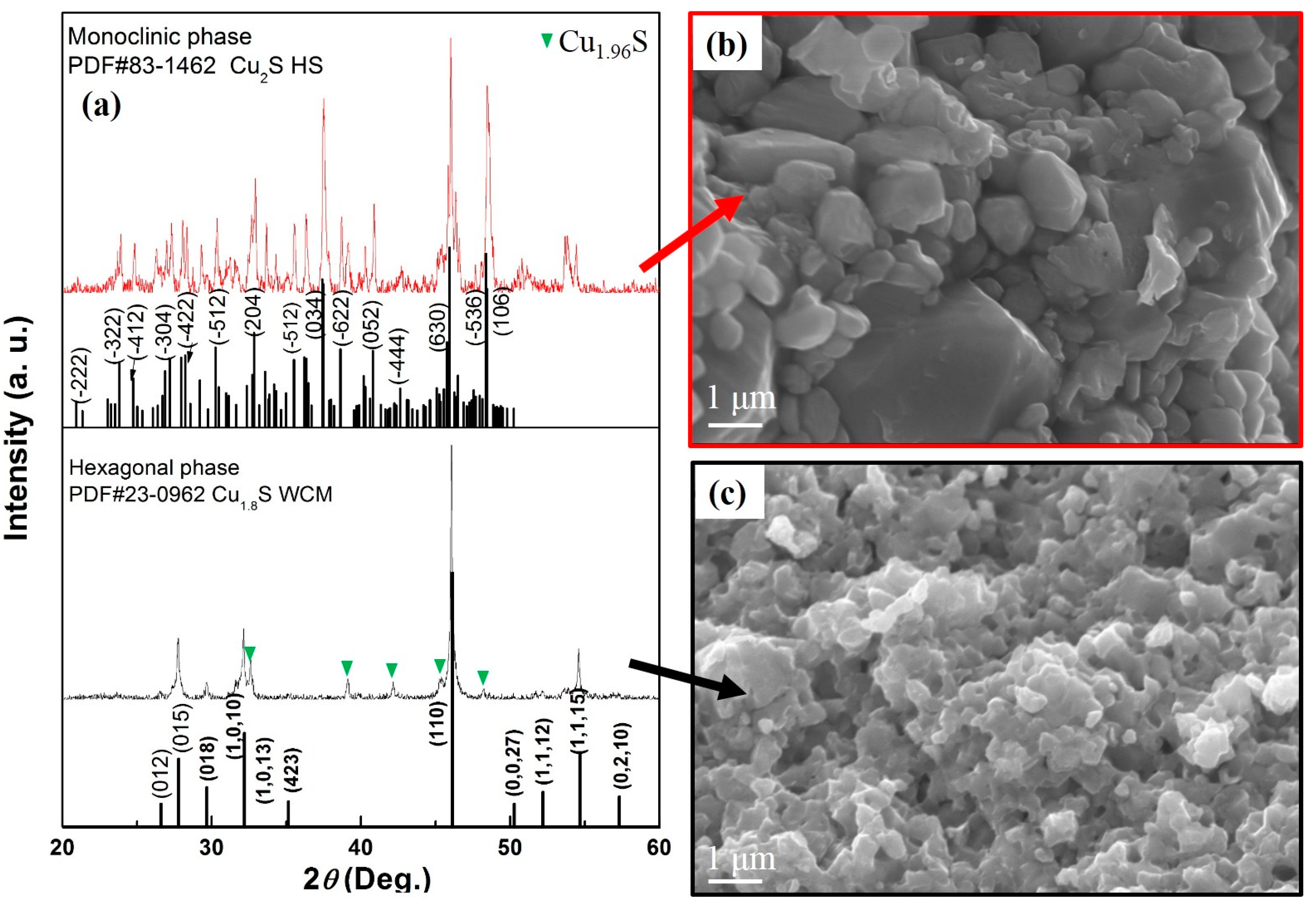
Figure 6.
Temperature dependence of electrical conductivity (a); Seebeck coefficient (b); and power factor (c) for the two bulk samples and the reference [34].
Figure 6.
Temperature dependence of electrical conductivity (a); Seebeck coefficient (b); and power factor (c) for the two bulk samples and the reference [34].
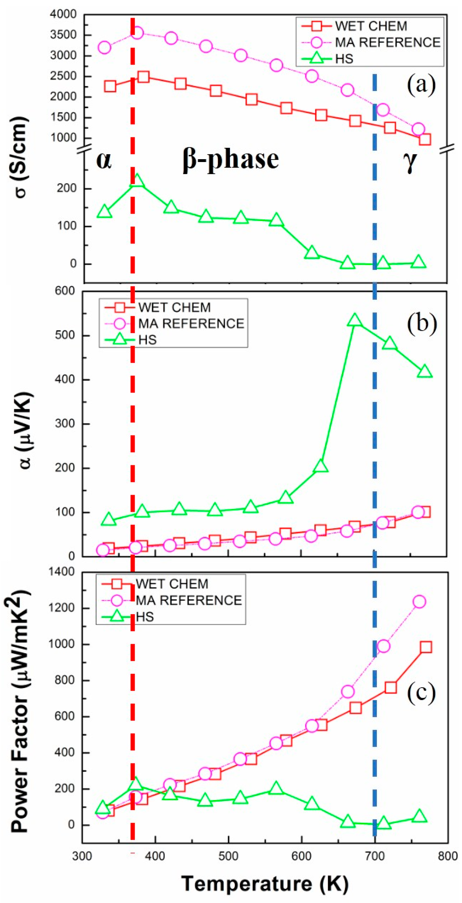
Figure 7.
Temperature dependence of thermal conductivity (a) for the two bulk samples and ZT value and (b) for the two bulk samples and the reference [34].
Figure 7.
Temperature dependence of thermal conductivity (a) for the two bulk samples and ZT value and (b) for the two bulk samples and the reference [34].
© 2017 by the authors. Licensee MDPI, Basel, Switzerland. This article is an open access article distributed under the terms and conditions of the Creative Commons Attribution (CC BY) license (http://creativecommons.org/licenses/by/4.0/).
Share and Cite
MDPI and ACS Style
Tang, Y.-Q.; Ge, Z.-H.; Feng, J. Synthesis and Thermoelectric Properties of Copper Sulfides via Solution Phase Methods and Spark Plasma Sintering. Crystals 2017, 7, 141. https://doi.org/10.3390/cryst7050141
AMA Style
Tang Y-Q, Ge Z-H, Feng J. Synthesis and Thermoelectric Properties of Copper Sulfides via Solution Phase Methods and Spark Plasma Sintering. Crystals. 2017; 7(5):141. https://doi.org/10.3390/cryst7050141
Chicago/Turabian StyleTang, Yun-Qiao, Zhen-Hua Ge, and Jing Feng. 2017. "Synthesis and Thermoelectric Properties of Copper Sulfides via Solution Phase Methods and Spark Plasma Sintering" Crystals 7, no. 5: 141. https://doi.org/10.3390/cryst7050141
Note that from the first issue of 2016, this journal uses article numbers instead of page numbers. See further details here.