Letter

Effects of In0.82Ga0.18As/InP Double Buffers Design on the Microstructure of the In0.82G0.18As/InP Heterostructure

1
Key Lab of Automobile Materials Ministry of Education, College of Materials Science and Engineering, Jilin University, Changchun 130025, China
2
State Key Lab for Mechanical Behavior of Materials, College of Materials Science and Engineering, Xi’an Jiaotong University, Xi’an 710049, China
*
Author to whom correspondence should be addressed.
Crystals 2017, 7(6), 155; https://doi.org/10.3390/cryst7060155
Submission received: 10 April 2017 / Revised: 16 May 2017 / Accepted: 22 May 2017 / Published: 25 May 2017
(This article belongs to the Special Issue Epitaxial Growth of Semiconductor Nanostructures)

Abstract

:
In order to reduce the dislocation density and improve the performance of high indium content In0.82Ga0.18As films, the design of double buffer layers has been introduced into the In0.82Ga0.18As/InP heterostructure. Compared with other buffer layer structures, we introduce an InP thin layer, which is the same as the substrate, into the In0.82Ga0.18As/InP heterostructure. The epitaxial layers and buffer layers were grown by the low-pressure metalorganic chemical vapor deposition (LP-MOCVD) method. In this study, the surface morphology and microstructures of the heterostructure were investigated by SEM, AFM, XRD and TEM. The residual strains of the In0.82Ga0.18As epitaxial layer in different samples were studied by Raman spectroscopy. The residual strain of the In0.82Ga0.18As epitaxial layer was decreased by designing double buffer layers which included an InP layer; as a result, dislocations in the epitaxial layer were effectively suppressed since the dislocation density was notably reduced. Moreover, the performance of In0.82Ga0.18As films was investigated using the Hall test, and the results are in line with our expectations. By comparing different buffer layer structures, we explained the mechanism of dislocation density reduction by using double buffer layers, which included a thin InP layer.

1. Introduction

The ternary III–V compounds InxGa1−xAs (0 < x < 1) with features such as relatively high carrier density, wide direct band gap ranging from 0.35 to 1.42 eV, high reliability and radiation resistance [1,2,3,4,5], have wide applications in short-wave infrared photodetectors [6,7,8,9] and solar cells [10,11]. Particularly, high indium content InxGa1−xAs (x = 0.82) detectors with a cut-off wavelength of more than 2 μm applied in aerospace imaging (such as earth observation, remote sensing and environmental monitoring, etc.) and spectroscopy attract more interest [12]. InP and GaAs substrates have been commonly used for the growth of InxGa1−xAs films [13,14,15]. However, the lattice mismatch between the epitaxial layers and substrates strongly affects the performance of the In0.82Ga0.18As films. The lattice mismatch between the In0.82Ga0.18As and InP is 2%, whereas in the In0.82Ga0.18As/GaAs heterostructure it is greater than 5.6% [16]. So, InP is often used as the preferred substrate material, however, the lattice mismatch is still too large to obtain a good In0.82Ga0.18As film. So, in order to obtain high quality In0.82Ga0.18As/InP (100) structures, the lattice defect formation due to misfit remains a major problem that needs to be solved. The insertion of buffer layers (with the same composition as the epitaxial layer or graded buffer layers for relevant components with epitaxial layers) [12,17,18] between the substrate and the epitaxial layer is a common and critical approach used to improve the quality of epitaxial layers. However, there is little research done on the buffer layer associated with the substrate material, especially for InxGa1−xAs/InP heterostructures.
In a previous study, we discussed the relationship between dislocations and microstructure in In0.82Ga0.18As/InP heterostructures without a buffer layer [19]. In this experiment, to release the strain and obtain a better In In0.82Ga0.18As film, a thin In0.82Ga0.18As layer was employed as a buffer for InP-based In0.82Ga0.18As. Additionally, we introduced a thin InP layer as a buffer between the In0.82Ga0.18As buffer layer and InP substrate. We believe that the thin InP layer can play a role in reducing dislocation in the epitaxial layer. We expected that the dislocation density would be reduced by the epitaxial layer growth. We designed three different buffer layer structures for comprehensive comparison in order to verify our assumptions. The effects of different buffers on the material quality and performance of thw In0.82Ga0.18As/InP (100) heterostructure were investigated. Based on TEM images of the three typical structures, the dislocation formation mechanism was also investigated. The results will be helpful for understanding dislocation behaviors in the growth of the heterostructure with relatively high lattice mismatch, and further in the design of appropriate buffer layers for fabrication of high indium content InxGa1−xAs with a high carrier density.

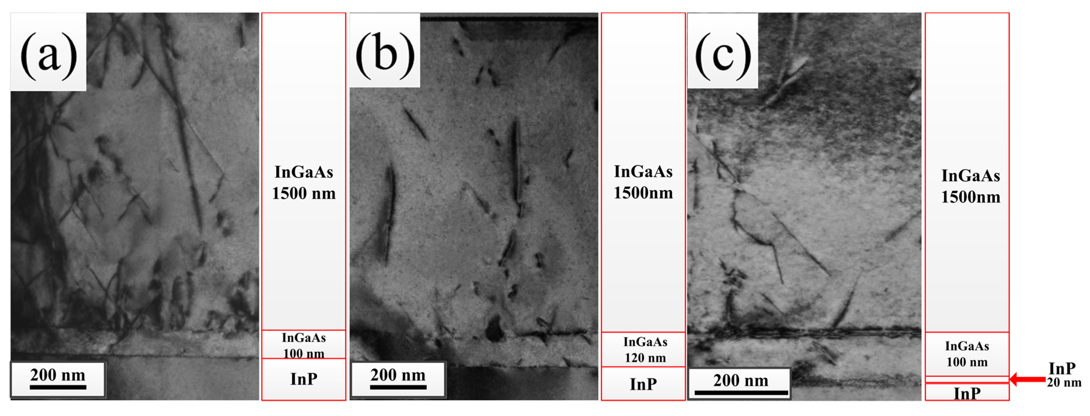
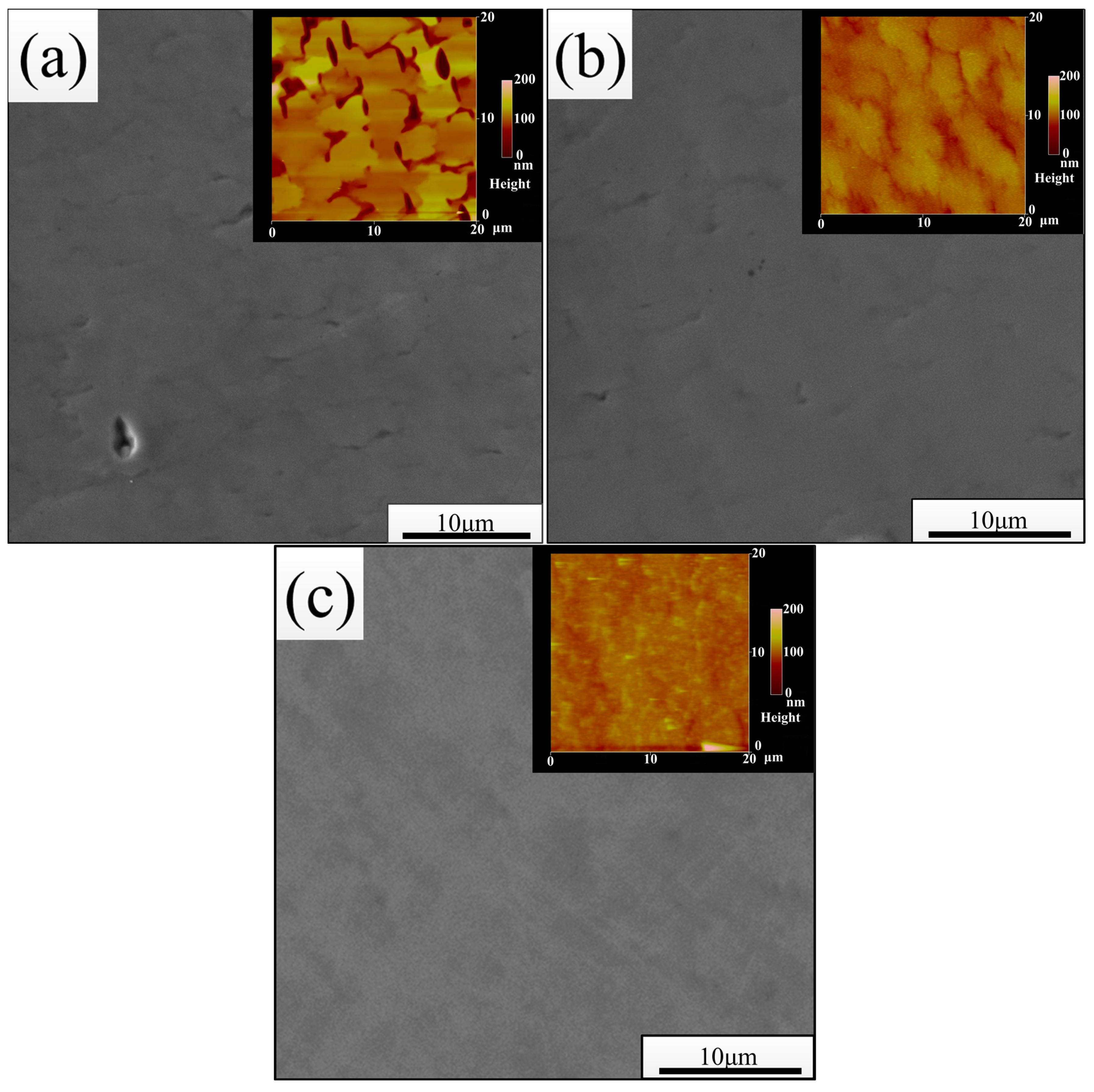
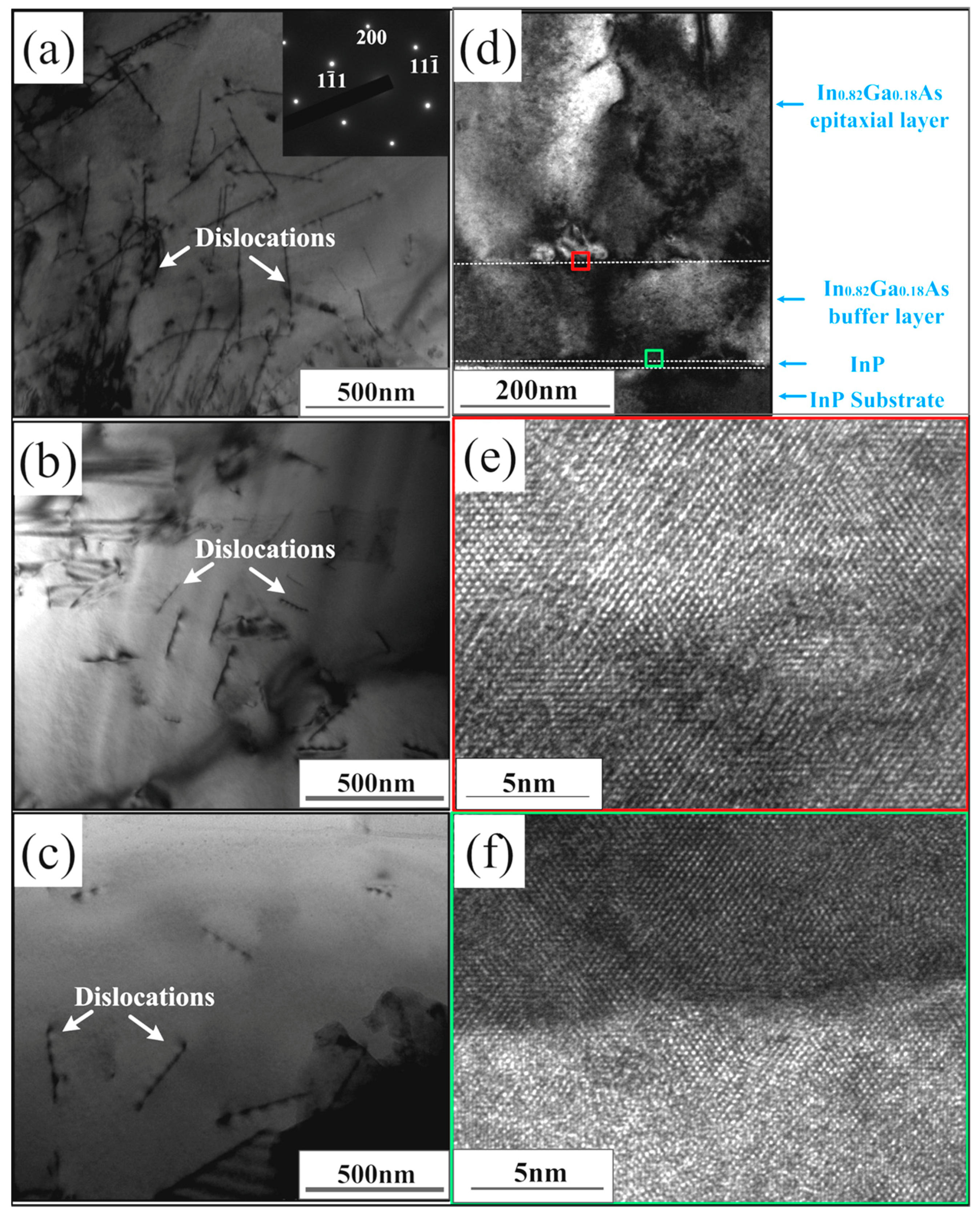
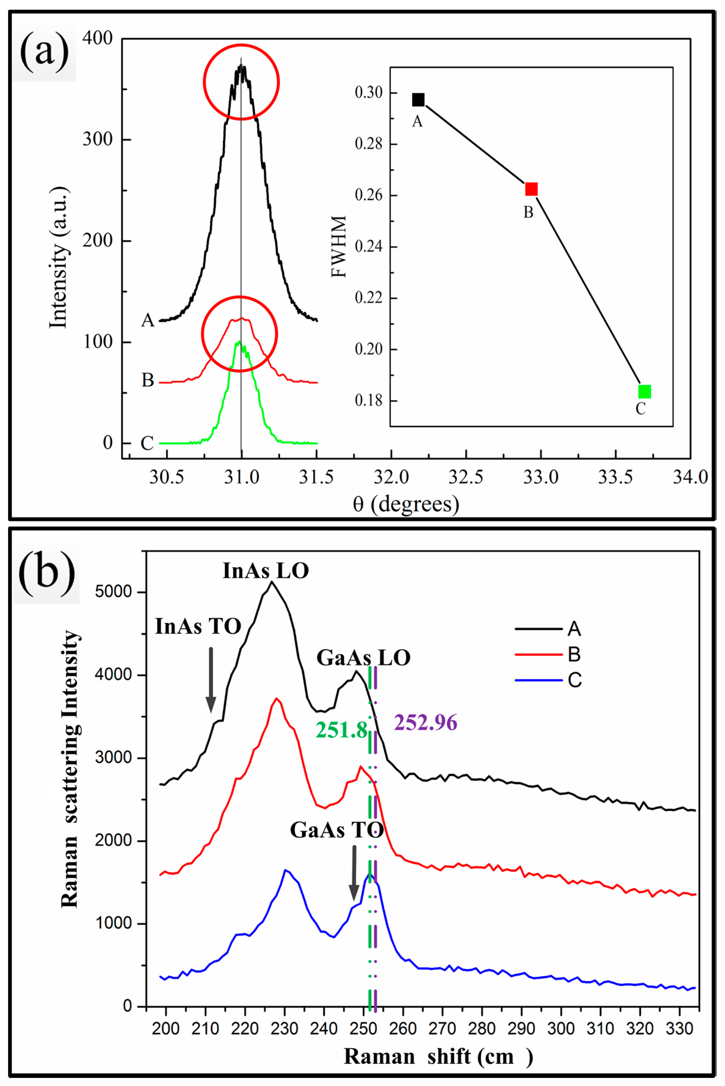
2. Results and Discussion

In order to better verify and clarify the unique role of the InP buffer layer, we designed three different kinds of buffer layer structures and compared them. Based on their structures, the three samples were labelled as sample A, B and C, respectively (see Materials and Methods or Figure 1 for details).
As shown in Figure 1, the epitaxial layer of the sample C had the least number of dislocations. So, we proposed that the double buffer layers’ structure, especially the thin InP layer, could play a unique role in improving the performance. The quality of a semiconductor always has a relationship with the surface morphology. This is because the surface morphology of the epitaxial layer is strongly related to dislocations in the epitaxial layer. In order to verify our assumption that sample C had the best surface morphology, the surface morphology and roughness of the In0.82Ga0.18As epitaxial layers were examined by SEM and AFM. As shown in Figure 2, small holes or shallow stripes in Figure 2c are fewer than in Figure 2a,b. Also, the surface roughness of the samples was obtained by software analysis. The surface roughness of the three samples was 17.3, 11.0 and 7.4 nm, respectively. The values are consistent with the SEM results. As a result, the surface becomes smoother with the insertion of the InP layer. Therefore, we believe that sample C has the minimum number of dislocations in the epitaxial layer.
In general, while the dislocation density is used to characterize the number of dislocations, the full width at half maximum (FWHM) is used to characterize the crystalline quality and dislocation density of the thin films. The full width at half maximum (FWHM) of In0.82Ga0.18As epitaxial layers was obtained from the (004) X-ray rocking curves (RCs), as shown in Figure 3a. The FWHM of the In0.82Ga0.18As epitaxial layers decreases as the thickness of the buffer layer increases. However, with the insertion of the InP layer, the FWHM of the In0.82Ga0.18As epitaxial layer decreased more obviously than the increasing thickness of the single buffer layer. It was shown that the insertion of a InP thin layer improved the quality of the In0.82Ga0.18As epitaxial remarkably. Moreover, as shown in Figure 3a, in the X-ray 004 curve, the peaks were at the same angle among these wafers; by careful contrast, the peak positions of the rocking curves of the three samples did not coincide completely (enlarge the Figure 3a), which showed that the stress had an influence on the lattice constant.
The smallest FWHM of 0.183° was obtained in sample C, which provided the best crystalline quality. Moreover, based on the value of FWHM, we could calculate the dislocation density of the epitaxial layers according to the following formula [20,21]:
Ndis = 2 (FWHM)2/9a02
where FWHM is in radians, and a0 is the lattice constant of the epitaxial layer. In this paper, a0 = 5.9584 Å. Based on the above results, it was calculated that the In0.82Ga0.18As epitaxial layer of the sample C with the smallest FWHM had the minimum dislocation density. The obtained values of the dislocation density are presented in Table 1. The dislocation densities in different regions (at the interface and the surface), also calculated by the IFFT method [19], are given in Table 1.
In the case of the lattice mismatch between the In0.82Ga0.18As epitaxial layers and the InP substrate, mismatch stress in the epitaxial layer is very important for the surface morphology, microstructure and properties of the sample. Strain relaxation has been investigated by means of Raman scattering in In0.82Ga0.18As epitaxial layers under the (111) back-scattering geometry. Furthermore, it is confirmed that the thickness (1.5 μm) of In0.82Ga0.18As epitaxial layers is far beyond the penetration depth. Based on the study of Raman scattering of InxGa1−xAs materials, due to a limitation of the scattering selection rule, in the In0.82Ga0.18As epitaxial layer of sphalerite structure will appear different phonon modes under different back-scattering geometry. Under a (011) back-scattering geometry, there is only the TO mode, and under the (100) back scattering there is only the LO mode without the TO mode, but the two modes will appear in the (111) back scattering. In Figure 3, strong peaks corresponding to InAs-like LO and GaAs-Like LO phonons and weak peaks corresponding to InAs-like TO and GaAs-TO phonons are observed. Usually, these weak peaks are obscure as configuration appears in the left shoulders of the InAs-like LO frequency and GaAs-Like LO frequency [22]. A strong and sharp peak corresponding to InAs-like LO is due to the high content of In. The InAs-like LO frequencies remained near 233 cm−1 in InxGa1−xAs Raman scattering, and the GaAs-like LO frequency varied with the In content [23].
The relationship between the frequency shift of GaAs-like LO of the InxGa1−xAs film and stress in the epitaxial layer is:
F = 3 Ω L O ω 0 / [ ( S 11 + 2 S 12 ) ( p + 2 q ) ( S 11 S 12 ) ( p q ) ]
Ω L O = Ω L O ω 0 L O
ω0LO = −32.4x2 − 18.6x + 290
where F is the strength of the residual strain which is summarized in Table 1; ω 0 L O is the frequency of InxGa1−xAs epitaxial material in stress-free condition; Ω L O is the actual measured value of GaAs-like LO frequency; ω0 is the optical phonon frequency at k = 0; p and q are optical phonon deformation constants; S11 and S12 are elastic constants; x is In constant [22,24,25,26].
Because x = 0.82, the calculated ω 0 L O is 252.96 cm−1. As shown in Figure 3 and presented in Table 1, the positions of the GaAs-like LO peaks were not very close to each other with the shift differing by about 3 cm−1 and sample C had the smallest value of Ω L O . As a result, all these numbers were negative, which represented the direction of the stresses. However, the stresses in the epitaxial layer of different samples have the following relationship: Fa < 0, Fb < 0, Fc < 0, Fa > Fb > Fc. Small residual strain leads to little dislocations required to release it and the surface morphology becomes better. This result is consistent with the FWHM and the SEM (or AFM) images.
Moreover, high resolution transmission electron microscopy (HRTEM) was used to analyze the microstructure of the epitaxial and buffer layers more visually. We chose the cross-section TEM images that were under the same axial to better illustrate the experimental results of dislocation reduction. In Figure 4a–c, a lot of dislocations interlaced together; with increasing thickness of the buffer layer and insertion of the InP layer, the number of dislocations was reduced obviously. In the previous report, the dislocation types (60° and 90° dislocations) at the interface were analyzed in detail [27,28]. In Figure 4d–e, we have shown the interfaces of different regions of sample C. It is shown that little dislocations existed at the interface of the epitaxial layer and buffer layer. We calculated the dislocation density at different regions (near the interface and near the surface) of the three samples by the IFFT (magnified inverse fast Fourier transform) method. The results are presented in Table 1. The value of dislocation density at the interface between the two buffer layers (12.7 × 1010 cm−2) was much larger than that at the interface between the buffer layer and epitaxial layer (2.44 × 1010 cm−2), which indicated that dislocations in sample C were strongly confined in the InP buffer. It led to the least surface dislocation density value in sample C. These results are in agreement with the results calculated by Formula (1). Due to no lattice mismatch between the epitaxial layer and the buffer layer, the interface boundary was not very clear. No lattice mismatch results in no misfit stress and misfit dislocations. The threading dislocations are directly related to the multiplication of the misfit dislocations in the buffer layer or the multiplication of the dislocations during the epitaxial layer growth process. The above argument is still applicable to the InP buffer layer and substrate.
We think that the insertion of the thin InP layer reduced the misfit stress between the In0.82Ga0.18As buffer and substrate due to no lattice mismatch between the InP buffer layer and substrate. So, with this design of double buffer layers, there was no lattice mismatch not only between the epitaxial and buffer layers but also between the buffer layer and the InP substrate. Moreover, insertion of the thin InP layer prevented the movement of defects, especially dislocations from the substrate to the buffer layer, thereby reducing the source of the dislocations in the buffer layer. As a result, the density of dislocations in the In0.82Ga0.18As epitaxial was reduced. However, although there is a lattice mismatch between the two buffer layers, the misfit stress between the two buffer layers was less than that between the In0.82Ga0.18As buffer layers and the InP substrate, and the In0.82Ga0.18As buffer was relatively thick enough to suppress the motion of the misfit dislocation compared with the InP buffer layer. So, the misfit stress and the strength of the residual strain were both reduced. As a result, the misfit dislocations were limited in the In0.82Ga0.18As/InP double buffers and the threading dislocations are effectively suppressed. Hence, the best surface morphology and performance of the In0.82Ga0.18As epitaxial layer was obtained.
In order to test the performance of the samples, and verify our hypothesis, we did the Hall test. Table 2 shows the results of the Hall test for all three samples at 300 K. Because the values of the Hall coefficient are negative, the In0.82Ga0.18As epitaxial layers are n-type semiconductor materials. Of all samples, sample C still had the largest carrier density and the smallest resistivity although other parameters were similar in all samples. Sample C can be regarded as having the best electric property performance. Hence, sample C was found to have the best surface morphology and performance of the In0.82Ga0.18As epitaxial layer. This finding is consistent with our hypothesis.

3. Materials and Methods

3.1. Sample Preparation

Before the growth of the epitaxial layers, the In0.82Ga0.18As buffer layer or In0.82Ga0.18As and InP buffer layers were introduced into the structure under the same growth conditions at 703 K. The buffer layers were grown by low-pressure MOVCD (AIXTRON 200/4). Three heterostructures (A–C samples) were grown with different buffer structures: sample A only with a thin In0.82Ga0.18As buffer layer for 100 nm; sample B with an In0.82Ga0.18As buffer layer for 120 nm; and sample C with a 100 nm In0.82Ga0.18As buffer layer in addition to another thin InP buffer total for 120 nm (Figure 1). The In0.82Ga0.18As epitaxial layers in these samples were also grown by low-pressure MOVCD with a thickness of 1500 nm at 923 K. TMGa, TMIn and 10% arsine (AsH3) in H2 were used as precursors. Palladium-diffused hydrogen was used as a carrier gas. The substrates on the graphite susceptor were heated under inductively coupled radio frequency power. The reactor pressure was maintained at 1 × 10⁴ Pa.

3.2. Characterization Techniques

After growth, the morphologies of the three samples were observed by atomic force microscopy (AFM, Multimode 8, Berlin, Germany) and a scanning electron microscopy (SEM, VEGA 3, Tescan, Brno Czech). A high-resolution X-ray diffractometer (XRD, D8, Bruker, Berlin, Germany) was used for the FWHM measurements to investigate the crystalline quality of the epitaxial layers. The samples for TEM observations were prepared using the FIB technique. Transmission electron microscopy (TEM, JEM-2100F, JEOL, Toyko, Japan) operated at 200 KV was used for TEM observations; high resolution transmission electron microscopy (HRTEM) was used to observe cross-section samples. Raman scattering spectroscopy (UV-Horiba, Tokyo, Japan) and Hall tester (Lake-7704A, Lower Lake, CA, USA) were used to measure the stress and Hall effect of the samples.

4. Conclusions

In summary, we investigated the surface morphology and microstructure by XRD, AFM, Raman spectroscopy and TEM. We also verified the semiconductor performance by the Hall test. These data testify to our assumptions and standpoints. We explain the role of the InP buffer layer. The results showed that for the high In content In0.82Ga0.18As/InP system, the buffer layer was effective for relieving the crystalline quality deterioration of the epitaxial layer due to a large lattice mismatch. In particular, the design of double buffer layers including an InP layer more effectively suppressed the formation of the misfit dislocations for no lattice mismatch between the buffer layer and the epitaxial layer (or substrate) compared with increasing the thickness of a single In0.82Ga0.18As buffer layer. The experimental results showed that it is feasible to reduce the dislocation density and improve the quality of the epitaxial layer by introducing In0.82Ga0.18As/InP double buffer layers with the same substrate material. Despite a relatively good In0.82Ga0.18As film obtained in this study there is still a need for further investigation to estimate the most suitable thickness of the double buffer layers’ design.

Acknowledgments

The authors gratefully acknowledge Guoqing Miao for providing the samples of the experiment. And the authors gratefully acknowledge financial support from the National Nature Science Foundation (No. 61474053), the National Key Basic Research Project of China (973 Project, No.2012CB619200), the 2014 Natural Science Basic Research Open Foundation of the Key Lab of Automobile Materials, Ministry of Education, Jilin University (No. 1018320144001) and the State Key Laboratory for Mechanical Behavior of Materials, Xi’an Jiaotong University (No. 20161806).

Author Contributions

Zuo-xing Guo, Xiangdong Ding and Liang Zhao conceived and designed the experiments; Jing-juan Li and Liang Zhao performed the experiments; Liang Zhao and Lei Zhao analyzed the data; Shen Yang and Min Zhang contributed analysis tools; Liang Zhao and Lei Zhao wrote the paper.

Conflicts of Interest

The authors declare no conflict of interest.

References

  1. Vurgaftman, I.; Meyer, J.R.; Ram-Mohan, L.R. Band parameters for iii-v compound semiconductors and their alloys. J. Appl. Phys. 2001, 89, 5815–5875. [Google Scholar] [CrossRef]
  2. Del Alamo, J.A. Nanometre-scale electronics with iii-v compound semiconductors. Nature 2011, 479, 317–323. [Google Scholar] [CrossRef] [PubMed]
  3. Arslan, Y.; Oguz, F.; Besikci, C. Extended wavelength swir ingaas focal plane array: Characteristics and limitations. Infrared Phys. Technol. 2015, 70, 134–137. [Google Scholar] [CrossRef]
  4. Ajayan, J.; Nirmal, D. A review of inp/inalas/ingaas based transistors for high frequency applications. Superlattices Microstruct. 2015, 86, 1–19. [Google Scholar] [CrossRef]
  5. Kim, J.; Fischetti, M.V. Electronic band structure calculations for biaxially strained Si, Ge, and III-V semiconductors. J. Appl. Phys. 2010, 108, 013710. [Google Scholar] [CrossRef]
  6. Li, C.; Zhang, Y.; Wang, K.; Gu, Y.; Li, H.; Li, Y. Distinction investigation of ingaas photodetectors cutoff at 2.9 μm. Infrared Phys. Technol. 2010, 53, 173–176. [Google Scholar] [CrossRef]
  7. Chen, X.Y.; Gu, Y.; Zhang, Y.G.; Xi, S.P.; Guo, Z.X.; Zhou, L.; Li, A.Z.; Li, H. Optimization of inalas buffers for growth of gaas-based high indium content ingaas photodetectors. J. Cryst. Growth 2015, 425, 346–350. [Google Scholar] [CrossRef]
  8. Tsai, C.L.; Cheng, K.Y.; Chou, S.T.; Lin, S.Y. Ingaas quantum wire infrared photodetector. Appl. Phys. Lett. 2007, 91, 181105. [Google Scholar] [CrossRef]
  9. Xia, H.; Li, T.X.; Tang, H.J.; Zhu, L.; Li, X.; Gong, H.M.; Lu, W. Nanoscale imaging of the photoresponse in pn junctions of ingaas infrared detector. Sci. Rep. 2016, 6, 21544. [Google Scholar] [CrossRef] [PubMed]
  10. Tzeng, T.E.; Chuang, K.Y.; Lay, T.S.; Chang, C.H. Broadband ingaas quantum dot-in-a-well solar cells of p-type wells. J. Cryst. Growth 2013, 378, 583–586. [Google Scholar] [CrossRef]
  11. Gao, F.; Wen, L.; Li, J.; Guan, Y.; Zhang, S.; Li, G. Achieving high-quality In0.3Ga0.7As films on gaas substrates by low-temperature molecular beam epitaxy. CrystEngComm 2014, 16, 10774–10779. [Google Scholar] [CrossRef]
  12. Zhang, Y.; Gu, Y.; Tian, Z.; Li, A.; Zhu, X.; Zheng, Y. Wavelength extended 2.4μm heterojunction ingaas photodiodes with inalas cap and linearly graded buffer layers suitable for both front and back illuminations. Infrared Phys. Technol. 2008, 51, 316–321. [Google Scholar] [CrossRef]
  13. Tounsi, N.; Habchi, M.M.; Chine, Z.; Rebey, A.; El Jani, B. Optical properties study of In.08Ga.92As/gaas using spectral reflectance, photoreflectance and near-infrared photoluminescence. Superlattices Microstruct. 2013, 59, 133–143. [Google Scholar] [CrossRef]
  14. Tsai, J.-H. Investigation of inp/ingaas metamorphic co-integrated complementary doping-channel field-effect transistors for logic application. Superlattices Microstruct. 2014, 65, 256–263. [Google Scholar] [CrossRef]
  15. Samonji, K.; Yonezu, H.; Takagi, Y.; Ohshima, N. Evolution process of cross-hatch patterns and reduction of surface roughness in (inas)[sub m](gaas)[sub n] strained short-period superlattices and ingaas alloy layers grown on gaas. J. Appl. Phys. 1999, 86, 1331. [Google Scholar] [CrossRef]
  16. Chang, S.Z.; Chang, T.C.; Lee, S.C. The growth of highly mismatched inxga1−xas (0.28 ≤ x ≤ 1) on gaas by molecular-beam epitaxy. J. Appl. Phys. 1993, 73, 4916–4926. [Google Scholar] [CrossRef]
  17. Li, J.; Miao, G.; Zhang, Z.; Zeng, Y. Experiments and analysis of the two-step growth of ingaas on gaas substrate. CrystEngComm 2015, 17, 5808–5813. [Google Scholar] [CrossRef]
  18. Zhang, T.; Miao, G.; Jin, Y.; Jiang, H.; Li, Z.; Song, H. Effect of buffer growth temperature on crystalline quality and optical property of In0.82Ga0.18As/InP grown by lp-mocvd. J. Alloy. Compd. 2008, 458, 363–365. [Google Scholar] [CrossRef]
  19. Zhao, L.; Guo, Z.; Wei, Q.; Miao, G.; Zhao, L. The relationship between the dislocations and microstructure in In0.82Ga0.18As/Inp heterostructures. Sci. Rep. 2016, 6, 35139. [Google Scholar] [CrossRef] [PubMed]
  20. Liu, X.; Song, H.; Miao, G.; Jiang, H.; Cao, L.; Li, D.; Sun, X.; Chen, Y. Influence of thermal annealing duration of buffer layer on the crystalline quality of In0.82Ga0.18As grown on inp substrate by lp-mocvd. Appl. Surf. Sci. 2011, 257, 1996–1999. [Google Scholar] [CrossRef]
  21. Chang, S.Z.; Chang, T.C.; Shen, J.L.; Lee, S.C.; Chen, Y.F. Material and electrical properties of highly mismatched in x ga1-x as on gaas by molecular-beam epitaxy. J. Appl. Phys. 1993, 74, 6912–6918. [Google Scholar] [CrossRef]
  22. Emura, S.; Gonda, S.-I.; Matsui, Y.; Hayashi, H. Internal-stress effects on raman spectra of inxga1-xas on inp. Phys. Rev. B 1988, 38, 3280–3286. [Google Scholar] [CrossRef]
  23. Nicholas, R.J.; Brunel, L.C.; Huant, S.; Karrai, K.; Portal, J.C.; Brummell, M.A.; Razeghi, M.; Cheng, K.Y.; Cho, A.Y. Frequency-shifted polaron coupling in Ga0.47In0.53As heterojunctions. Phys. Rev. Lett. 1985, 55, 883–886. [Google Scholar] [CrossRef] [PubMed]
  24. Feng, Z.C.; Allerman, A.A.; Barnes, P.A.; Perkowitz, S. Raman scattering of ingaas/inp grown by uniform radial flow epitaxy. Appl. Phys. Lett. 1992, 60, 1848–1850. [Google Scholar] [CrossRef]
  25. Jusserand, B.; Voisin, P.; Voos, M.; Chang, L.L.; Mendez, E.E.; Esaki, L. Raman scattering in gasb-alsb strained layer superlattices. Appl. Phys. Lett. 1985, 46, 678–680. [Google Scholar] [CrossRef]
  26. Cerdeira, F.; Buchenauer, C.J.; Pollak, F.H.; Cardona, M. Stress-induced shifts of first-order raman frequencies of diamond- and zinc-blende-type semiconductors. Phys. Rev. B 1972, 5, 580–593. [Google Scholar] [CrossRef]
  27. Zhao, L.; Sun, J.G.; Guo, Z.X.; Miao, G.Q. Tem dislocations characterization of inxga1-xas/inp (100) (x = 0.82) on mismatched inp substrate. Mater. Lett. 2013, 106, 222–224. [Google Scholar] [CrossRef]
  28. Dimitrakopulos, G.P.; Bazioti, C.; Grym, J.; Gladkov, P.; Hulicius, E.; Pangrác, J.; Pacherová, O.; Komninou, P. Misfit dislocation reduction in ingaas epilayers grown on porous gaas substrates. Appl. Surf. Sci. 2014, 306, 89–93. [Google Scholar] [CrossRef]
Figure 1. Cross-sectional TEM images of the three samples with different buffer layer structures, (a) Sample A; (b) Sample B; (c) Sample C.
Crystals 07 00155 g001
Figure 2. (ac) show the SEM and AFM images of In0.82Ga0.18As epitaxial layers grown with different buffer layer structures.
Crystals 07 00155 g002
Figure 3. (a) Comparison between the rocking curves of the In0.82Ga0.18As epitaxial layers for samples A–C; (b) Raman spectra of the In0.82Ga0.18As epitaxial layers for samples A–C.
Crystals 07 00155 g003
Figure 4. TEM images for samples A–C with different buffer structures. (ac) cross-sectional views of the In0.82Ga0.18As epitaxial layers which were with different preparation buffer structures under the same axial; (d) cross-sectional view of sample C; (e) high-resolution image between the epitaxial and buffer layers of sample C; (f) high-resolution image between the double buffer layers of sample C.
Crystals 07 00155 g004
Table 1. Variation of full width at half maximum (FWHM); dislocation density Ndis (Ndis from rocking curves); frequency shift between Ω L O and ω0 ( Ω L O ); strength of the residual strain (F); dislocation density of the interface between the epitaxial layer and buffer layer ρi; dislocation density of the surface ρsi and ρs from IFFT of TEM, for Sample C; ρi1 is the dislocation density of the interface between the two buffer layers; ρi2 is the dislocation density of the interface between the epitaxial layer and buffer layers).
SamplesFWHM (Degree)Ndis (×109 cm−2) Ω L O (cm−1) Ω L O (cm−1)F (×106N·cm−2)ρi (×1010 cm−2)ρs (×1010 cm−2)
A0.2981.69248.74.26−1.9175.442.78
B0.2621.31250.52.46−1.1063.431.54
C0.1830.64251.81.16−0.490112.7 (ρi1)0.69
2.44 (ρi2)
Table 2. Results of Hall test of the three samples at 300 K.
SamplesResistivity (×10−6 Ω/cm)Hall Coefficient/RH (×10−2 cm−3C−1)Carrier Density/nH (×1020 cm−3)Hall Mobility/uH (×103 cm2(V·s)−1)Type
A6.6782−1.11055.62141.6718n
B6.5794−1.08805.73901.6331n
C6.5581−1.05595.91331.5973n

