Article

Morphology of Diamond Layers Grown on Different Facets of Single Crystal Diamond Substrates by a Microwave Plasma CVD in CH4-H2-N2 Gas Mixtures

by
Evgeny E. Ashkinazi
1,
Roman A. Khmelnitskii
2,3,4,
Vadim S. Sedov
1,
Andrew A. Khomich
1,3,
Alexander V. Khomich
1,2,3,* and
Viktor G. Ralchenko
1,5
1
Prokhorov General Physics Institute, Russian Academy of Sciences, Vavilova Str. 38, Moscow 119991, Russia
2
Lebedev Physical Institute, Russian Academy of Sciences, Leninskii Av. 53, Moscow 119991, Russia
3
Kotelnikov Institute of Radio Engineering and Electronics, Russian Academy of Sciences, Vvedenskogo Sq. 1, Fryazino 141190, Russia
4
Troitsk Institute for Innovation and Fusion Research, Pushkovykh Str. 12, Troitsk, Moscow 142190, Russia
5
Harbin Institute of Technology, 92 Xidazhi Str., Harbin 150001, China
*
Author to whom correspondence should be addressed.
Crystals 2017, 7(6), 166; https://doi.org/10.3390/cryst7060166
Submission received: 30 April 2017 / Revised: 29 May 2017 / Accepted: 31 May 2017 / Published: 6 June 2017
(This article belongs to the Special Issue Diamond Crystals)

Abstract

:
Epitaxial growth of diamond films on different facets of synthetic IIa-type single crystal (SC) high-pressure high temperature (HPHT) diamond substrate by a microwave plasma CVD in CH4-H2-N2 gas mixture with the high concentration (4%) of nitrogen is studied. A beveled SC diamond embraced with low-index {100}, {110}, {111}, {211}, and {311} faces was used as the substrate. Only the {100} face is found to sustain homoepitaxial growth at the present experimental parameters, while nanocrystalline diamond (NCD) films are produced on other planes. This observation is important for the choice of appropriate growth parameters, in particular, for the production of bi-layer or multilayer NCD-on-microcrystalline diamond (MCD) superhard coatings on tools when the deposition of continuous conformal NCD film on all facet is required. The development of the film morphology with growth time is examined with SEM. The structure of hillocks, with or without polycrystalline aggregates, that appear on {100} face is analyzed, and the stress field (up to 0.4 GPa) within the hillocks is evaluated based on high-resolution mapping of photoluminescence spectra of nitrogen-vacancy NV optical centers in the film.

1. Introduction

High hardness and abrasion resistance of diamond make it indispensable for machining of many materials such as composites and abrasive alloys, which leads to widespread use of diamond-based tools. Diamond coatings (DCs) produced by chemical vapor deposition (CVD) on tungsten carbide WC-Co cutting tools allow a great improvement in the tool performance by extending its lifetime, increasing the machining speed, and providing a better quality of the machined material [1]. The application of bilayered or multilayered micro- and nanocrystalline DCs further enhances the cutting tools’ functional properties [2,3]. The upper nanocrystalline layer provides low roughness and low friction coefficient, as well as high bending strength [4]. The bottom layer is typically deposited in the microcrystalline diamond growth regime since it has better adhesion to the WC-Co substrate, coupled to higher hardness [5]. Moreover, compared with single-layer DCs, bilayered DCs have higher heat conductivity and increased resistance to cracking [6].
The structure of a DC deposited in microwave plasma can be controlled by varying the composition of the gas mixture during the process run. For example, the addition of nitrogen allows a transition from microcrystalline diamond (MCD) to nanocrystalline diamond (NCD) coating deposition regimes. As a result, one can obtain smooth bilayered DCs with increased wear resistance by the CVD method for an optimal nitrogen concentration [3]. The N2 gas added to standard CH4-H2 mixtures strongly enhances the growth rate SC diamond seeds (typically of {100} orientation) [7,8], thus reducing the cost of CVD diamond production. In case of epitaxial growth of single crystals the growth rate and defect abundance depend on the diamond substrate face orientation, a less number of the defects forming on {100} facets [9]. Particularly, dislocation density can be significantly reduced by a lateral growth on {100} oriented substrate with a hole intentionally perforated in it as recently shown by Tallaire et al. [10].
The growth of nanocrystalline diamond on a microcrystalline diamond film has several differences from the more widely used growth on non-diamond substrates, including: (a) significant roughness of the microcrystalline film surface; (b) microcrystalline film is formed by crystallites with different faces, predominantly with {111} and {100} [11]; (c) no preliminary nucleation (seeding) is performed; and (d) there is no incubation period for growth [11]. This raises the question of possible differences of secondary nucleation and growth of nanocrystalline DCs on different faces of microcrystals of diamond films. We note that the deposition of ultrananocrystalline diamond (UNCD) films with grain typically, less than 10 nm, in a multicomponent gaseous environment, Ar-CH4-H2+N2 mixtures, on polished coarse-grained polycrystalline diamond plates (the grains with random orientation and size of 60–90 μm) was reported in [12]. The UNCD growth was assumed to start epitaxially, but the high rate of secondary nucleation very rapidly transformed the film to nanocrystalline structure uniformly over the substrate area. No impact of grain orientation of the substrate on the morphology of the deposited UNCD layer was observed.
In the production of bilayer coatings of such type, it is important to deposit the NCD layer uniformly on all facets of the grains in underlying MCD film, independent on the facet orientation. The goal of the present study is the investigation of the nucleation and growth processes of DCs on different facets of a diamond single crystal as a model substrate, and examination of the growth defects on the {100} face with SEM and photoluminescence (PL) spectroscopy. To this end, we prepare faceted SC diamond substrates to deposit the diamond film simultaneously on facets of different orientations and compare the resulting morphologies for identical process parameters.

2. Experimental

The diamond coatings were synthesized in “hydrogen/methane/nitrogen” gas mixtures on SC diamond substrates using a microwave plasma CVD system ARDIS-100 (2.45 GHz, 5 kW) [13] with the following parameters: total gas flow rate of 500 sccm (H2:460/CH4:20/N2:20), pressure of 130 Torr, and microwave power of 2.8 kW. The substrate temperature during deposition was about 800 °C as measured through plasma by the Mikron M770 two-color pyrometer. These deposition parameters and the nitrogen concentration in the gas mixture corresponded to deposition regime for nanocrystalline DCs on WC-Co substrates [3]. As the substrate, we used a multifaceted type IIa synthetic SC diamond produced by the high pressure—high temperature (HPHT) gradient method. The upper part of the crystal exhibited smooth {311}, {211}, {111}, and {110} growth faces, with the larger {100} face on the top. This multifaceted part was cut off along the {100} plane to remove the bottom part containing sides with negative slope. The top and bottom {100} planes were polished to roughness Ra of less than 10 nm, as measured with an optical profilometer (ZYGO NewView 5000), while the other facets remained unpolished. The roughness Ra of the as-grown faces was 90–100 nm for {111}, 120–130 nm for {211}, 160–180 nm for {311} and 100–110 nm for {110} planes. The roughness was mainly due to growth steps on those surfaces. The substrate thickness was 0.9 mm, which provided almost identical growth conditions in the CVD reactor, with a minimized temperature gradient across the substrate. At least the adjacent regions around common edges between the facets had identical temperatures during diamond deposition.
A scanning electron microscope (SEM) JSM7001F (JEOL) was used to examine the coating surface morphology. The Raman and PL spectra, excited at 473 nm wavelength, were measured at room temperature with a LabRam HR840 (Horiba Jobin-Yvon) spectrometer in a confocal configuration with the spectral resolution of 0.5 cm−1 and spatial resolution of ~1 μm. The spatial mapping of the PL and Raman spectra over the coating surface area was carried out by placing the sample on a motorized table (MärzhäuserWetzlar) with positioning accuracy of about 0.5 μm.

3. Results and Discussion

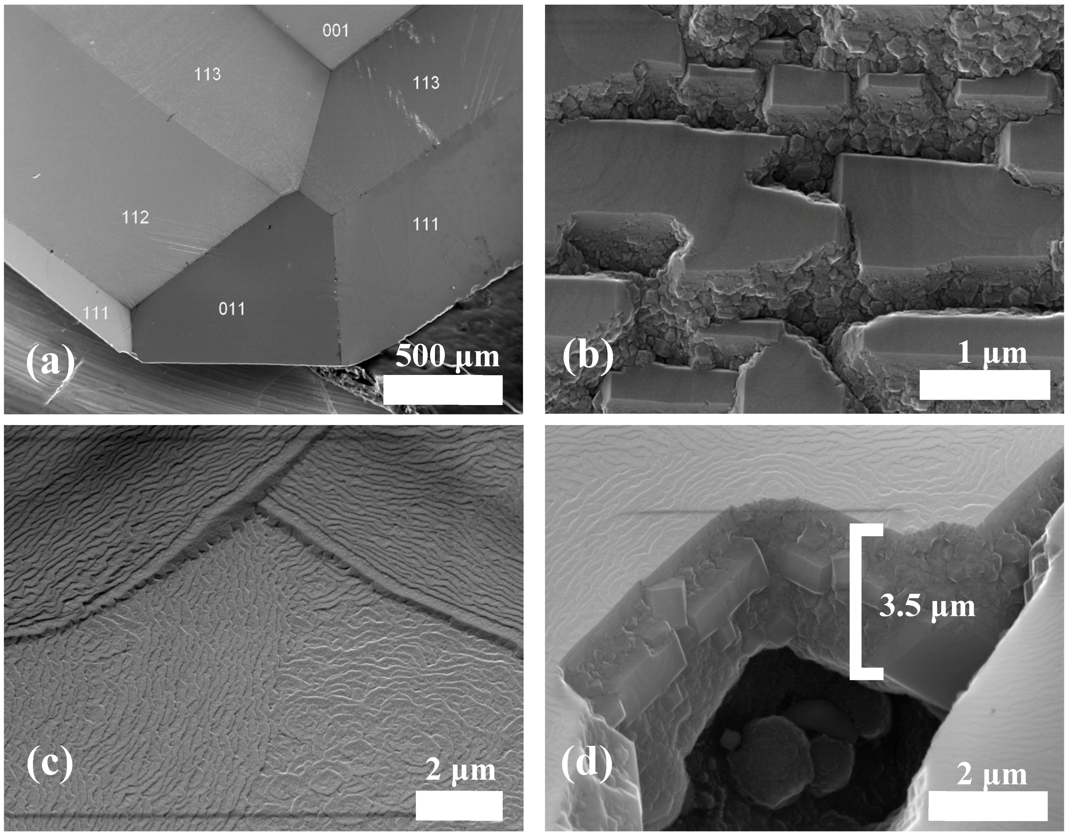
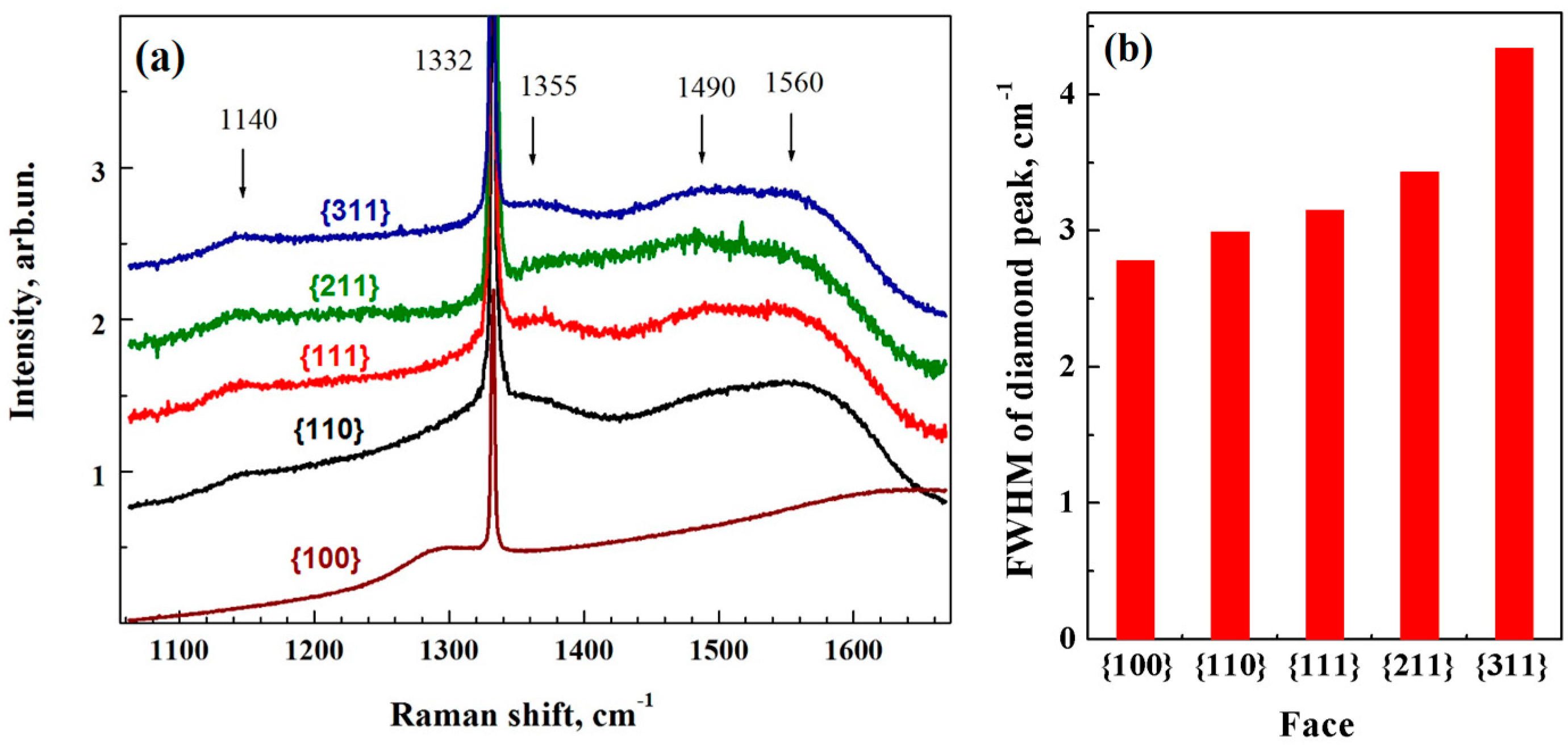
3.1. Diamond Deposition on Low-Index Facets of the Single Crystal Substrate

The SEM analysis shows that, under the growth conditions of nanocrystalline diamond (if a non-diamond substrate material is used), the NCD coating is formed on the {111} and {110} faces of the substrate from the very beginning. This coating is formed of grains with the size of a few tens to hundreds of nanometers. Figure 1 presents SEM images of several regions of the sample after 5 min of growth. The panoramic image in Figure 1a displays seven different faces on the HPHT diamond substrate. The original {311} and {211} faces did not contain regions with outcrops of {100} and {111} planes. However, clearly pronounced layers with {111} planes appear on those faces even at the initial growth stage, and, flat regions with {100} planes are formed, on the top of these layers. Figure 1b shows an example of surface relief formed on the {311} face. The surface morphologies of the coating grown on the {100} and {111} planes are essentially different: the {100} planes are smooth, and homoepitaxial growth in the step bunching regime [14] occurs on these planes, whereas, on the {111} planes nanocrystallites arise and develop into a rough film surrounding the {100} domains.
In the course of the deposition process, the evolution of crystallite morphology on the diamond film surface is controlled by growth rates V of the main low-index crystalline faces, first of all, {100} and {111}, as well as by the {110} and {311} faces [15]. According to the crystal growth laws the area fraction of the faces with minimum growth rate increases. The dimensionless parameter that characterizes the ratio of the growth rate of a low-index face to the growth rate of one of them, say, the {111} face is an alpha-parameter α = 3½V100/V111. The greater the α, the greater the fraction of the {111} faces area of the crystallite. A decrease in the substrate temperature during the CVD process leads to an increase in α and a decrease in the crystallite size [15]. An increase in the methane [CH4] concentration in the gas mixture leads to an increase in the growth rate and the α parameter, a decrease in the crystallite size, and an increase in the probability of secondary nucleation, i.e., the formation of new nuclei of diamond crystallites with different crystalline orientation on the diamond surface [13]. This hydrocarbon supersaturation facilitates the growth of the nanocrystalline film. The increase in [CH4] increases the concentration of hydrocarbon radicals (CH3, CH2, CH, etc.) and their adsorption rate on the growing surface of diamond. This increases the probability of deposition of two growth radicals side by side, including radicals with two (CH2) or three (CH) free bonds, that promotes the formation of growth defects and crystalline nuclei with a different orientation. Nitrogen addition to the growth mixture also increases the diamond growth rate, among other things, due to the growth of the probability of formation of two-dimensional nuclei on the growing surface, and increases α and the probability of secondary nucleation [16]. The mechanism is similar because an atom of N embedded on the surface of diamond has two or more free bonds [15]. For large α, nanocrystallites are formed mainly by {111} faces, which are prone to twinning due to low twin formation energy [17], therefore, multiple twinning on the {111} planes determines the morphology of the nanocrystalline films.
It is believed that renucleation processes dominate under low power density or high methane concentration [11]. The observed film morphology, growth rate, and crystal size can be rationalized using a model based on the competition of H atoms, CH3 radicals, and other CHx (CH2, CH, C) species to react with dangling bonds on the surface [18]. Under the CVD conditions, the concentration of CH3 radicals in gas is much higher than the concentration of other CHx radicals. It is generally accepted that the key role in diamond growth is played by the CH3 radicals [18]. The CH3 radical is relatively large and, due to steric hindrance, it is hard to be coupled to a free bond on the growing surface. This stage is assumed to limit the growth rate. The CH3 radical coupled to the surface loses one H atom when interacting with atomic hydrogen and turns into a CH2 group that can migrate along the growing surface [19]. This group reaches the growth step and completes the construction of the crystal. Other CHx radicals are also coupled to free bonds. The resulting group may have a free bond. It is most probable that an atomic or molecular hydrogen is coupled to this group. However, there is a probability that another CHx radical will be bonded. This may introduce a surface defect with a different symmetry of bonds, which gives rise to renucleation or a twin. In this model, the radical concentration ratios [CH3]/[H] and [CHx]/[CH3] determine the probability of the renucleation event. One should take in to account the difference between the probabilities of bonding of CHx radicals on different crystalline planes. Our experiments call into question the idea that, under the growth conditions of a nanocrystalline film, renucleation occurs on the growth surfaces of any orientation [20]. On the {100} face of SC substrate, homoepitaxial growth in the step bunching regime occurs for a long (5 min) period of time (Figure 1c,d). The concentrations of active radicals [H], [CH3], [CH2], [CH], and [C] near the {100} and {111} growth surfaces are the same, however, the growth morphologies on these surfaces are essentially different. According to the model [19], this means that the probability of incorporation of CH3 radical in {100} plane is much higher than that in {111} plane.
Figure 1c demonstrates epitaxial character and growth steps of the {100} face. The growth steps directions may change locally (Figure 1c); however, in some places they form twisted helical structures in the form of hillocks (presumably, around screw dislocations). The steps height amounts to tens of nanometers, but sometimes they become thicker. Such case occurs when one growth layer overtakes another to form a growth layer of increased thickness (Figure 1c). There is an assumption [21] that the formation of macrosteps occurs when the growth rate of atomic steps becomes of the order of the diffusion rate of adsorbed species along the surface. Ideally, the macrosteps have atomically smooth surfaces [22]. The accumulation of thickened growth layers increases the roughness of the growth surface {100}.
Figure 1d demonstrates the growth lacunae on the face {100}, on which one can measure the thickness of a homoepitaxial film grown in 5 min. This thickness of 3.5 μm corresponds to the growth rate of 42 μm/h for the {100} face. Without the addition of N2, the epitaxial growth rate at 4% CH4 and 800 °C of about 5 μm/h was reported for the {100} face [23]. In other words, the addition of 4% of N2 to the gas mixture increases the growth rate by an order of magnitude, in agreement with other publications [7,15].
At the end of the 5-min growth session, we measured the Raman spectra (Figure 2a) of the films deposited on each face of the sample [3]. The Raman spectrum on the face {100} contains only the 1st order Raman diamond line at νR = 1332.4 cm−1 with full width at half magnitude (FWHM) Γ1/2 = 2.7 cm−1. On other faces, the spectrum contains also broad bands of disordered carbon with maxima at 1355 and 1560 cm−1 (D and G bands), as well as trans-polyacetylene (TPA) bands with maxima at 1140 and 1490 cm−1, which are characteristic of NCD.
The width of the diamond peak in the Raman spectrum increases in the series {100} → {110} → {111} → {211} → {311} from 2.7 to 4.3 cm−1 (Figure 2b). The diamond 1332 cm−1 peak broadens as a result of defects presence, and also due to a nonuniform stress. The peak shift is caused by a stress, tensile or compressive, depending on the shift sign. From the diamond Raman peak shift ΔνR, we estimated the stress σ in the film according to relationship σ [GPa] = ΔνR [0.38 GPa/cm−1] for hydrostatic stress [24], the positive or negative values of σ corresponding to compressive or tensile strength, respectively. For the {100} and {211} faces, the position of this peak corresponds to unstressed diamond. For the {111} and {110} faces, the shift of the diamond peak corresponds to the compressive stress of 0.15 GPa, while, for the {311} face the tensile stress of 0.3–0.6 GPa is assessed. The ratio of summed intensities of the TPA and G bands to the area of the diamond peak increases in the series {100} → {211} → {111} ≈ {110} → {311} according to the increase of the fraction of non-diamond phase in the film.
Figure 3 demonstrates the images of the same sample after 70-min growth on the same substrate. There are no smooth epitaxial regions on {211} faces of the substrate (Figure 3a), all of them have been coated with NDC film. In contrast, on {311} faces, there still remain islands with smooth {100} oriented growth surfaces, although the area of these regions was reduced in comparison with 5-min growth sample (compare Figure 1b and Figure 3a,b). The nanocrystallites (Figure 3b) are formed mainly by a multiple twinning mechanism both upon parallel {111} planes and by rotating the orientation of the twinned crystal at 70.5 degrees about the {110} axis. The size of the twin crystallites on {311} and {211} faces reaches hundreds of nanometers (Figure 3b). On {111} and {110} faces, the twinning manifests itself weaker, the secondary nucleation dominates [9], and the crystallite size does not exceed 100 nm.

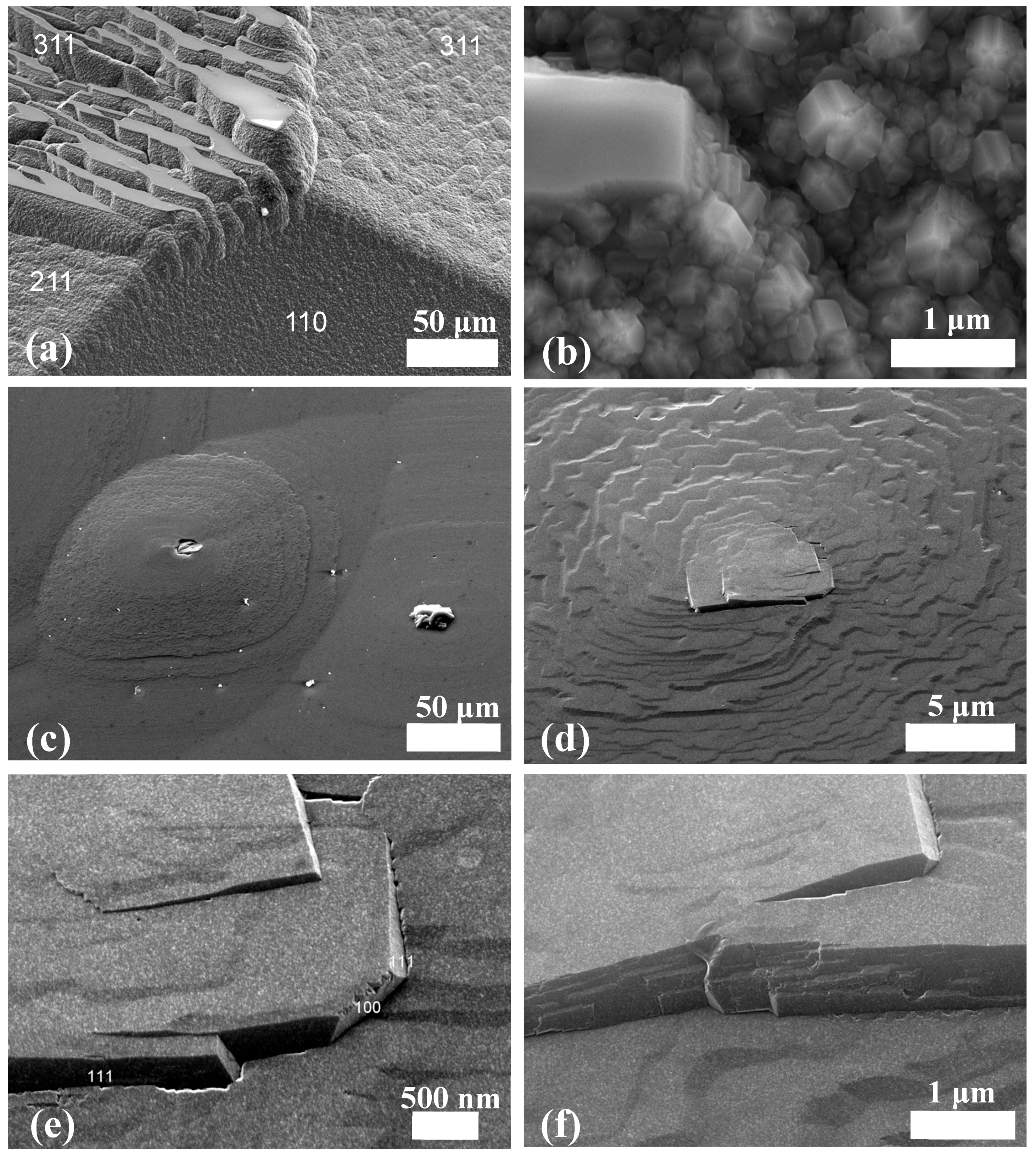
3.2. Polycrystalline Aggregations at {100} Face

In contrast to other low-index faces, {100} planes continue growing predominantly by the step bunching growth mechanism, even with relatively long deposition times. The area fraction of the {100} planes decreased with the growth time, hence, the {100} faces grow with the maximum rate. This observation agrees with the assumption that the probability of CH3 radical embedding in the {100} plane is much higher than that for other planes. The enhanced growth of layered screw structures on {100} face (Figure 3c) gives rise to hillocks [26]. As the film grows, at the top of such structures, as well as at the intersections of thickened growth steps of different directions, polycrystalline aggregations arise and develop (Figure 3c). Figure 3d–f show the initial stage of this process. One can see that growth steps become thicker and their edges become rougher. A great role in this process is played by nitrogen impurity, which is the main impurity in both natural and synthetic diamond produced by CVD and HPHT processes [27]. The incorporation efficiency of nitrogen in diamond lattice is as low as 10−4 [28,29]. Therefore, nitrogen is concentrated on the growing surface, contaminates and roughens the growth steps [30]. The end faces of the thickest growth macrosteps eventually acquire crystalline faceting, predominantly by {111} and {110} faces (Figure 3e). Gradually, a relief is developed on these faces (Figure 3f), on which twins readily form. The twins give rise to polycrystalline aggregates; these inclusions also may arise when lacunae (like those shown in Figure 1d) are overgrown near the defects or contaminations of the substrate.

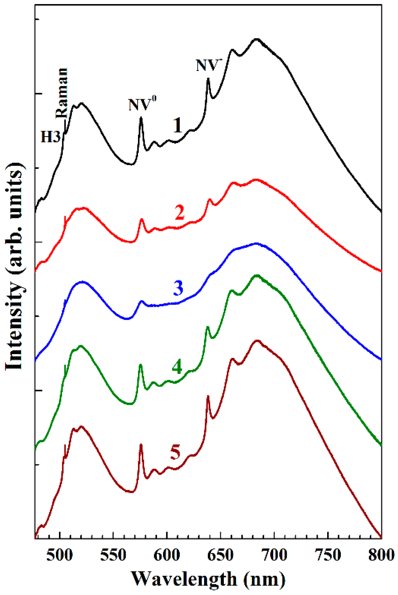
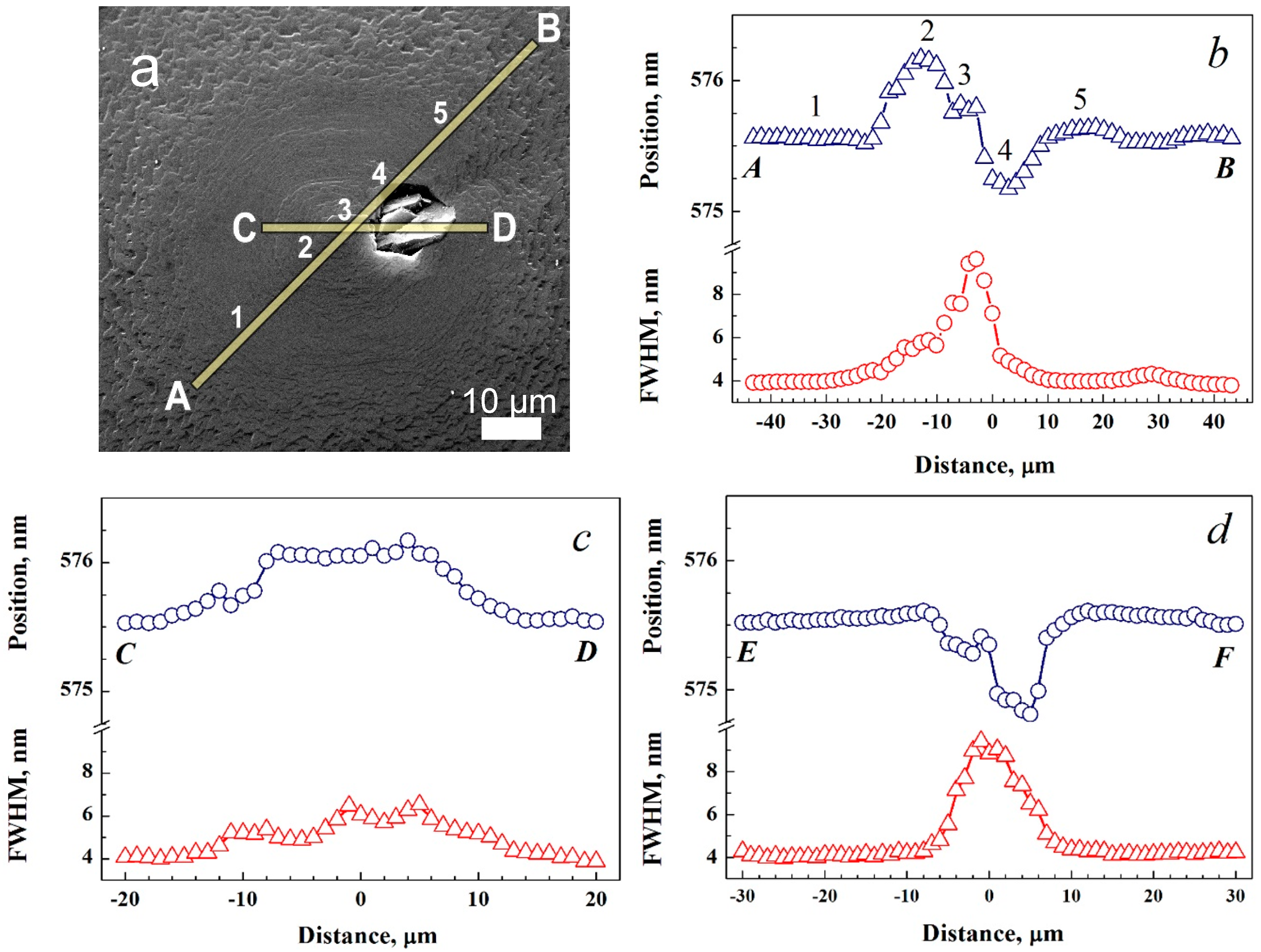
3.3. Photoluminescence Scanning Spectroscopy on Growth Defects on {100} Face

Growth hillocks and non-epitaxial crystallites are often observed on homoepitaxial CVD diamond films. The hillock formation is believed to be caused by stacking faults or dislocations that nucleate at the interface between the surface and the epitaxial layer from lattice defects or propagate from the substrate into the CVD layer [31,32]. Those defects induce a surface roughness, facilitate incorporation of impurities, crystalline imperfections, and non-diamond phases. The hillocks could be responsible for dielectric breakdown effect and current leakage in diamond-based electronic devices which constitute the main limitations to their development and improvement of device properties. The problem of surface growth defects is not so relevant in the case of deposition of bilayer micro/nanocrystalline diamond coatings for cutting tools. Meanwhile, the features of the formation mechanism and stress state of the growth defects in CVD homoepitaxial films are still debatable. In order to examine stress distribution of such defects, we measured spatially resolved photoluminescence and Raman spectra.
Figure 4 displays the PL spectra taken at on {100} face on a hillock shown in Figure 5a, along the line A-B across the hillock, from foot to the top and further. The spectra are normalized to the integral intensity of the diamond band at 505 nm in the Raman spectrum. The PL spectra show three optical centers with zero phonon lines (ZPL) at wavelengths of 575 nm (NV0 defect), 637 nm (NV defect), and 503 nm (H3 defect). The optical centers at 575 and 637 nm are formed by defects containing one nitrogen atom and one vacancy in neutral and negative charge states, respectively [25]. The NV defects are usually detected in CVD diamond films grown with the addition of nitrogen. However, the H3 optical center, formed by the 2NV0 defect, two nitrogen atoms and a vacancy in a neutral charge state, is less common in CVD diamond, because during growth nitrogen atoms are introduced into the crystal lattice one by one, not in pairs. In HPHT diamonds, the enhanced concentration of H3 centers is observed in less-stressed regions of the crystal and near dislocations [33].
In CVD diamonds, the 2NV defect can be obtained by a long-term high-temperature post-growth annealing to cause aggregation of individual nitrogen atoms or NV defects via their diffusion [34,35]. Under the CVD conditions, the growth temperature and duration are considered insufficient for the diffusion of nitrogen atoms or NV defects. In the samples investigated, the 2NV defects are likely to be created immediately in process of diamond film deposition. This may occur, for example, as a result of incorporation of an N2 molecule or a random incorporation of two nitrogen atoms next to each other. As the deposition rate of homoepitaxial diamond film increases, the incorporation efficiency of impurities into diamond also increases [36], and, according to calculations [37], the formation energy of 2NV defects in synthesized diamond substantially decreases for high nitrogen concentrations.
Owing to the presence of a vacancy, the NV optical centers are characterized by high values of strain softening, a mechanical stress leads to a significant shift in the position of its ZPL [25]. We measured the position and the FWHM of ZPLs at 575 nm and 637 nm across two hillocks. One of them contained a non-epitaxial polycrystalline aggregate on the top (Figure 5a), while the second hillock (not shown here) had no such polycrystalline inclusion. The PL spectra were measured in 1 µm or 1.4 µm steps along the lines A-B (Figure 5b) and C-D (Figure 5c), respectively, crossing the hillock near the top. The PL mapping of the second hillock was performed along the line E-F (Figure 5d), again crossing its top. The Lorentz profiles were used for fitting ZPL in the PL spectra.
The positions and widths of NV ZPL at 575 nm appreciably differed at different locations on the hillocks and revealed a complex picture along the scanning lines (Figure 5b–d). In absence of polycrystalline inclusion, the ZPL position displays a blue shift around the hillock top and the line broadening by a factor of two (Figure 5b,d). In contrast, a red shift and smaller broadening of NV ZPL is observed when the laser scan crosses the polycrystalline aggregate along the C-D path (Figure 5c). Similar profiles for ZPL position and width were also obtained for 637 nm line of NV center (not shown in Figure 5). We attributed the observed broadening and the shift of the bands in the PL spectra to mechanical stresses in the hillock material. Spatial variations in nitrogen concentration could also cause a local stress. We estimated the stress σ from the shift Δλ of the ZPL maximum at 575 nm using the gauge factor of −0.57 GPa/nm [38]. Then, the maximum tensile stress of 0.4 GPa along the scan line A-B at point 2 (Figure 5a,b) was assessed, while the maximum compressive stress σ of 0.25 GPa corresponded to point 4 on this path.
The PL mapping along C-D line (Figure 5c) across the hillock center and non-epitaxial inclusion revealed a tensile stress in this region (the 575 nm peak shifts to longer wavelengths), the position and width of the 575 nm line correlating with the surface profile of the film. The PL mapping across the top of another hillock, having no polycrystalline inclusion, showed a different picture (Figure 5d). A stress at the hillock top causes the 575 nm peak shift by 0.75 nm to shorter wavelengths, corresponding to the compressive stress of about 0.4 GPa. A low tensile stress background is observed outside the hillock. A similar trend with PL ZPL shift and broadening was observed for NV center at 637 nm, but not shown here. In this context, we mention the observations by Bolshakov et al. [39] the stress and variations of PL intensity of SiV centers in {100} oriented Si-doped epitaxial CVD diamond film within hillocks with polycrystalline inclusions. Using the Raman and PL spectra mapping they found a strong compressive stress on the hillock tip and an order of magnitude enhancement in the PL intensity. Our mapping results for NV PL are in line with that work.
For natural diamonds, there are several observations indicating that after the dissolution in water-containing carbonate melts the appearance of surface hillocks is typical for crystals with the high level of internal strains. Orlov [40] noted that the hillocks are often located along the intersecting striation associated with the bands of plastic deformation in diamond. Using polarized light microscopy, it was established [41] that in bulk of the crystals strongly strained regions are identified which borders coincide with the borders of the hillocks. The use of PL and Raman 3D mapping could facilitate assessment of the type and magnitude of stress within such features.

4. Conclusions

We demonstrated that the morphology of diamond films grown by a microwave plasma CVD on single crystal diamond substrates in CH4-H2-N2 in presence of high concentration of nitrogen strongly depends on the substrate’s crystallographic plane. The film structure on {100}, {110}, {111}, {211} and {311} faces has been examined with SEM, Raman and PL spectroscopy after a short (5 min) and prolonged (70 min) deposition time at conditions typically facilitated the formation of nanocrystalline diamond on foreign substrates. We found that only {100} face sustained homoepitaxial growth at the present experimental parameters, while only a nanocrystalline film is produced on other planes. Particularly, the NCD layer with the grain size of tens or hundreds of nanometers, often twinned, forms on {111}. This observation is important for the choice of appropriate growth parameters, in particular, for the production of bi-layer or multilayer NCD-on-MCD superhard coatings on tools, when the NCD deposition on all facets is required. The diamond epitaxy on {100} plane is possible even at high hydrocarbon and nitrogen contents in the process gas, that allows achievement of high growth rates of SC CVD diamond.
The growth of hillocks on {100} face proceeds in step-growth mode and is accompanied with the appearance of polycrystalline inclusions on the top. The early stage of the polycrystalline aggregates may include a faceting the step surface with {111} and {110} planes with further formation of the polycrystalline structure there. A tensile stress is revealed within polycrystalline inclusions on the hillocks from the shift of local PL spectra of NV optical centers, while a compressive stress is typical for the hillocks free of such inclusions. The PL spectroscopy mapping of the surface is shown to be a useful tool that allows measurement of the stress profile within growth defects in CVD diamond epitaxial films.

Acknowledgments

This work was supported by the Russian Scientific Fund (grant No. 15-19-00279).

Author Contributions

E.E.A. and R.A.K. conceived and designed the experiments; R.A.K., V.S.S. and A.A.K. performed the experiments; R.A.K. and A.V.K. analyzed the data; R.A.K., A.A.K. and V.G.R. wrote the paper.

Conflicts of Interest

The authors declare no conflict of interest.

References

  1. Polini, R.; Barletta, M.; Rubino, G.; Vesco, S. Advances in the Deposition of Diamond Coatings on Co-Cemented Tungsten Carbides. Adv. Mater. Sci. Eng. 2012, 2012, 151629. [Google Scholar] [CrossRef]
  2. Dumpala, R.; Chandran, M.; Rao, M.S.R. Engineered CVD Diamond Coatings for Machining and Tribological Applications. J. Miner. Met. Mater. Soc. 2015, 67, 1565–1577. [Google Scholar] [CrossRef]
  3. Khomich, A.A.; Ashkinazi, E.E.; Ralchenko, V.G.; Sedov, V.S.; Khmelnitskii, R.A.; Poklonskaya, O.N.; Kozlova, M.V.; Khomich, A.V. Application of Raman spectroscopy for the analysis of the structure of diamond coatings on a hard alloy. J. Appl. Spectrosc. 2017, 84, 297–304. [Google Scholar] [CrossRef]
  4. Chromik, R.R.; Winfrey, A.L.; Lüning, J.; Nemanich, R.J.; Wahl, K.J. Run-in behavior of nanocrystalline diamond coatings studied by in situ tribometry. Wear 2008, 265, 477–489. [Google Scholar] [CrossRef]
  5. Sun, F.; Ma, Y.; Shen, B.; Zhang, Z.; Chen, M. Fabrication and application of nano-microcrystalline composite diamond films on the interior hole surfaces of Co cemented tungsten carbide substrates. Diam. Relat. Mater. 2009, 18, 276–279. [Google Scholar] [CrossRef]
  6. Shafer, L.; Hofer, M.; Kroger, R. The versatility of hot-filament activated chemical vapor deposition. Thin Solid Films 2006, 515, 1017–1024. [Google Scholar] [CrossRef]
  7. Chayahara, A.; Mokuno, Y.; Horino, Y.; Takasu, Y.; Kato, H.; Yoshikawa, H.; Fujimori, N. The effect of nitrogen addition during high-rate homoepitaxial growth of diamond by microwave plasma CVD. Diam. Relat. Mater. 2004, 13, 1954–1958. [Google Scholar] [CrossRef]
  8. Tallaire, A.; Achard, J.; Silva, F.; Brinza, O.; Gicquel, A. Growth of large size diamond single crystals by plasma assisted chemical vapour deposition: Recent achievements and remaining challenges. Comptes Rendus Phys. 2013, 14, 169–184. [Google Scholar] [CrossRef]
  9. Lloret, F.; Fiori, A.; Araujo, D.; Eon, D.; Villar, M.P.; Bustarret, E. Stratigraphy of a diamond epitaxial three-dimensional overgrowth using doping superlattices. Appl. Phys. Lett. 2016, 108. [Google Scholar] [CrossRef]
  10. Tallaire, A.; Brinza, O.; Mille, V.; William, L.; Achard, J. Reduction of dislocations in single crystal diamond by lateral growth over a macroscopic hole. Adv. Mater. 2017, 29. [Google Scholar] [CrossRef] [PubMed]
  11. Koji, K. Diamond Films: Chemical Vapor Deposition for Oriented and Heteroepitaxial Growth; Elsevier: Amsterdam, The Netherlands, 2005; Chapter 5; pp. 31–50. [Google Scholar]
  12. Ralchenko, V.; Pimenov, S.; Konov, V.; Khomich, A.; Saveliev, A.; Popovich, A.; Vlasov, I.; Zavedeev, E.; Bozhko, A.; Loubnin, N.; et al. Nitrogenatednanocrystalline diamond films: Thermal and optical properties. Diam. Relat. Mater. 2007, 16, 2067–2073. [Google Scholar] [CrossRef]
  13. Bolshakov, A.P.; Ralchenko, V.G.; Yurov, V.Y.; Popovich, A.F.; Antonova, I.A.; Khomich, A.A.; Vlasov, I.I.; Ashkinazi, E.E.; Ryzhkov, S.G.; Vlasov, A.V.; et al. High-rate growth of single crystal diamond in microwave plasma in CH4/H2 and CH4/H2/Ar gas mixtures in presence of intensive soot formation. Diam. Relat. Mater. 2016, 62, 49–57. [Google Scholar] [CrossRef]
  14. Godbole, V.P.; Sumant, A.V.; Kshirsagar, R.B.; Dharmadhikari, C.V. Evidence for layered growth of (100) textured diamond films. Appl. Phys. Lett. 1997, 71, 2626–2628. [Google Scholar] [CrossRef]
  15. Silva, F.; Bonnin, X.; Achard, J.; Brinza, O.; Michau, A.; Secroun, A.; De Corte, K.; Felton, S.; Newton, M.; Gicquel, A. Single crystal CVD diamond growth strategy by the use of a 3D geometrical model: Growth on (113) oriented substrates. J. Cryst. Growth 2008, 310, 1067–1075. [Google Scholar] [CrossRef]
  16. Müller-Sebert, W.; Wörner, E.; Fuchs, F.; Wild, C.; Koidl, P. Nitrogen induced increase of growth rate in chemical vapor deposition of diamond. Appl. Phys. Lett. 1996, 68, 759–760. [Google Scholar] [CrossRef]
  17. Butler, J.E.; Oleynik, I. A mechanism for crystal twinning in the growth of diamond by chemical vapour deposition. Philos. Trans. R. Soc. A. 2008, 366, 295–311. [Google Scholar] [CrossRef] [PubMed]
  18. May, P.W.; Ashfold, M.N.R.; Mankelevich, Y.A. Microcrystalline, nanocrystalline, and ultrananocrystalline diamond chemical vapor deposition: Experiment and modeling of the factors controlling growth rate, nucleation, and crystal size. J. Appl. Phys. 2007, 101, 053115. [Google Scholar] [CrossRef]
  19. Richley, J.C.; Harvey, J.N.; Ashfold, M.N.R. CH2 Group Migration between H-Terminated 2 × 1 Reconstructed {100} and {111} Surfaces of Diamond. J. Phys. Chem. C 2012, 116, 7810–7816. [Google Scholar] [CrossRef]
  20. Barbosa, D.C.; Hammer, P.; Trava-Airoldi, V.J.; Corat, E.J. The valuable role of renucleation rate in ultrananocrystalline diamond growth. Diam. Relat. Mater. 2012, 23, 112–119. [Google Scholar] [CrossRef]
  21. Van der Putte, P.; Van Enckevort, W.J.P.; Giling, L.J.; Bloem, J. Surface morphology of HCl etched silicon wafers: II. Bunch formation. J. Cryst. Growth 1978, 43, 659–675. [Google Scholar] [CrossRef]
  22. Hayashi, K.; Yamanaka, S.; Okushi, H.; Kajimura, K. Homoepitaxial diamond films with large terraces. Appl. Phys. Lett. 1996, 68, 1220–1222. [Google Scholar] [CrossRef]
  23. Bushuev, E.V.; Yurov, V.Y.; Bolshakov, A.P.; Ralchenko, V.G.; Khomich, A.A.; Antonova, I.A.; Ashkinazi, E.E.; Shershulin, V.A.; Pashinin, V.P.; Konov, V.I. Express in situ measurement of epitaxial CVD diamond film growth kinetics. Diam. Relat. Mater. 2017, 72, 61–70. [Google Scholar] [CrossRef]
  24. Tardieu, A.; Cansell, F.; Petitet, J.P. Pressure and temperature dependence of the first-order Raman mode of diamond. J. Appl. Phys. 1990, 68, 3243–3245. [Google Scholar] [CrossRef]
  25. Zaitsev, A.M. Optical Properties of Diamond: A Data Handbook; Springer: Berlin, Germany, 2001. [Google Scholar]
  26. Sunagawa, I. Crystals: Growth, Morphology, and Perfection; Cambridge University Press: Cambridge, UK, 2005; pp. 44–45. [Google Scholar]
  27. Palyanov, Y.N.; Kupriyanov, I.N.; Khokhryakov, A.F.; Ralchenko, V.G. Crystal Growth of Diamond. In Handbook of Crystal Growth: Bulk Crystal Growth, 2nd ed.; Rudolph, P., Ed.; Elsevier: Amsterdam, The Netherlands, 2015. [Google Scholar]
  28. Samlenski, R.; Haug, C.; Brenn, R.; Wild, C.; Locher, R.; Koidl, P. Incorporation of nitrogen in chemical vapor deposition diamond. Appl. Phys. Lett. 1995, 67, 2798–2800. [Google Scholar] [CrossRef]
  29. Khomich, A.A.; Kudryavtsev, O.S.; Bolshakov, A.P.; Khomich, A.V.; Ashkinazi, E.E.; Ralchenko, V.G.; Vlasov, I.I.; Konov, V.I. Use of Optical Spectroscopy Methods to Determine the Solubility Limit for Nitrogen in Diamond Single Crystals Synthesized by Chemical Vapor Deposition. J. Appl. Spectrosc. 2015, 82, 242–247. [Google Scholar] [CrossRef]
  30. Yamada, H.; Chayahara, A.; Mokuno, Y. Effects of intentionally introduced nitrogen and substrate temperature on growth of diamond bulk single crystals. Jpn. J. Appl. Phys. 2016, 55. [Google Scholar] [CrossRef]
  31. Tallaire, A.; Kasu, M.; Ueda, K.; Makimoto, T. Origin of growth defects in CVD diamond epitaxial films. Diam. Relat. Mater. 2008, 17, 60–65. [Google Scholar] [CrossRef]
  32. Friel, I.; Clewes, S.L.; Dhillon, H.K.; Perkins, N.; Twitchen, D.J.; Scarsbrook, G.A. Control of surface and bulk crystalline quality in single crystal diamond grown by chemical vapor deposition. Diam. Relat. Mater. 2009, 18, 808–815. [Google Scholar] [CrossRef]
  33. Mccormick, T.L.; Jackson, W.E.; Nemanich, R.J. Strain and Impurity Content of Synthetic Diamond Crystals. In Materials Research Society Symposia Proceedings; Materials Research Society: Pittsburgh, PA, USA, 1994; Volume 349, pp. 445–450. [Google Scholar]
  34. Inyushkin, A.V.; Taldenkov, A.N.; Ralchenko, V.G.; Vlasov, I.I.; Konov, V.I.; Khomich, A.V.; Khmelnitskii, R.A.; Trushin, A.S. Thermal conductivity of polycrystalline CVD diamond: Effect of annealing-induced transformations of defects and grain boundaries. Phys. Status Solidi A 2008, 205, 2226–2232. [Google Scholar] [CrossRef]
  35. Jones, R.; Goss, J.P.; Pinto, H.; Palmer, D.W. Diffusion of nitrogen in diamond and the formation of A-centres. Diam. Relat. Mater. 2015, 53, 35–39. [Google Scholar] [CrossRef]
  36. Okushi, H.; Watanabe, H.; Ri, S.; Yamanaka, S.; Takeuchi, D. Device-grade homoepitaxial diamond film growth. J. Cryst. Growth 2002, 237–239, 1269–1276. [Google Scholar] [CrossRef]
  37. Deak, P.; Aradi, B.; Kaviani, M.; Frauenheim, T.; Gali, A. Formation of NV centers in diamond: A theoretical study based on calculated transitions and migration of nitrogen and vacancy related defects. Phys. Rev. B 2014, 89, 075203. [Google Scholar] [CrossRef]
  38. Fukura, S.; Nakagawa, T.; Kagi, H. High spatial resolution photoluminescence and Raman spectroscopic measurements of a natural polycrystalline diamond, carbonado. Diam. Relat. Mater. 2005, 14, 1950–1954. [Google Scholar] [CrossRef]
  39. Bolshakov, A.; Ralchenko, V.; Sedov, V.; Khomich, A.; Vlasov, I.; Khomich, A.; Trofimov, N.; Krivobok, V.; Nikolaev, S.; Khmelnitskii, R.; et al. Photoluminescence of SiV centers in single crystal CVD diamond in situ doped with Si from silane. Phys. Status Solidi A 2015, 212, 2525–2532. [Google Scholar] [CrossRef]
  40. Orlov, Y.L. The Mineralogy of Diamond; Wiley: New York, NY, USA, 1977; p. 235. [Google Scholar]
  41. Khokhryakov, A.F.; Palyanov, Y.N. Effect of crystal defects on diamond morphology during dissolution in the mantle. Am. Mineral. 2015, 100, 1528–1532. [Google Scholar] [CrossRef]
Figure 1. SEM images obtained after 5-min diamond deposition on high pressure—high temperature (HPTP) diamond substrate: (a) a corner part of the substrate with indicated crystallographic faces; (b) surface morphology of {311} face; (c) layer-by-layer growth on the {100} face; and (d) view of a lacuna at 45° angle on the face {100}.
Crystals 07 00166 g001
Figure 2. (a) Raman spectra on different faces after 5-min growth. The spectra are shifted along the vertical scale for clarity. Two broad bands at 1290 and 1650 cm−1 on {100} face are due to photoluminescence of H3 defect center [25]. The Raman spectra were normalized to the 1332.5 cm−1 peak intensity; (b) Diamond Raman peak width (FWHM) for CVD film on different faces.
Crystals 07 00166 g002
Figure 3. SEM images after 70-min growth on a single-crystal HPHT substrate: (a) the bevel of the substrate with indicated crystallographic faces; (b) {311} face at higher magnification; (c) stepped growth and formation of a hillock on the {100} face; (d) generation of a polycrystalline aggregate on the top of a hillock on the {100} face; (e) the same hillock, formation of low-index crystalline faces on edges of thick growth steps; (f) on the top of another hillock, a relief is developed on the edges of thick growth step.
Crystals 07 00166 g003
Figure 4. Photoluminescence spectra at five points (1)–(5) along the line A-B line crossing the top of the hillock, as shown in Figure 5a.
Crystals 07 00166 g004
Figure 5. SEM image of a hillock with polycrystalline inclusion on the top. The lines A-B and C-D, which avoid or cross the polycrystalline inclusion, respectively, denote the direction of PL NV mapping (a); Variations of position (top curve) and the FWHM (bottom curve) of NV0 ZPL at 575 nm along the lines A-B (b) and C-D (c); Variation position and width of PL at 575 nm peak along the line E-F crossing the top of another hillock without inclusions (d). The mapping step is 1.4 μm for A-B and 1 μm for C-D and E-F lines. The lines are guides for an eye. Locations # 1, 2…5 in (a,b) show positions where the PL spectra presented in Figure 4 have been taken.
Crystals 07 00166 g005

