
Evolution in Time of Radiation Defects Induced by Negative Pions and Muons in Crystals with a Diamond Structure

Moscow Institute of Physics and Technology, Institutsky lane 9, 141700 Dolgoprudny, Russia
Crystals 2017, 7(6), 174; https://doi.org/10.3390/cryst7060174
Submission received: 27 March 2017
/
Revised: 29 May 2017
/
Accepted: 9 June 2017
/
Published: 14 June 2017
(This article belongs to the Special Issue Diamond Crystals)
Abstract
:Evolution in time of radiation defects induced by negatively-charged pions and muons in crystals with diamond structures is considered. Negative pions and muons are captured by the nucleus and ionize an appropriate host atom, forming a positively-charged radiation defect in a lattice. As a result of an evolution in time, this radiation defect transforms into the acceptor center. An analysis of the full evolution process is considered for the first time. Formation of this acceptor center can be divided into three stages. At the first stage, the radiation defect interacts with a radiation trace and captures electrons. The radiation defect is neutralized completely in Si and Ge for a short time t s, but in diamond, the complete neutralization time is very large t s. At the second stage, broken chemical bonds of the radiation defect are restored. In Si and Ge, this process takes place for the neutral radiation defect, but in diamond, it goes for a positively-charged state. The characteristic time of this stage is s for Si and Ge and s for diamond. After the chemical bonds’ restoration, the positively-charged, but chemically-bound radiation defect in diamond is quickly neutralized because of the electron density redistribution. The neutralization process is characterized by the lattice relaxation time. At the third stage, a neutral chemically-bound radiation defect captures an additional electron to saturate all chemical bonds and forms an ionized acceptor center. The existence of a sufficiently big electric dipolar moment leads to the electron capture. Qualitative estimates for the time of this process were obtained for diamond, silicon and germanium crystals. It was sown that this time is the shortest for diamond (≤ s) and the longest for silicon (≤ s)
1. Introduction
Radiation defects in diamond and silicon are examined actively because these semiconductors are widely used as detectors and some other devices in high energy physics. The main problem of these investigations is connected with their radiation hardness (see e.g., some recent works [1,2,3,4,5,6]). Radiation defects induced by protons, neutrons and heavier particles with kinetic energies MeV are studied in most works. After slowing down to kinetic energies E less than ionization energies of host atoms in crystals, these impinging particles stop in the lattice, damaging it. If the recoil energy is higher than the lattice binding energy, a host atom will be displaced from its site. Numerical modeling of these processes is carried out, e.g., in [3,5]. In [7], many types of these radiation defects in diamond are well described. The second problem is implantation of ions in crystals for preparing necessary impurity atoms. Ion implantation is a commonly-used method for modifying properties of materials in the field of microelectronics. The application for diamond is represented, e.g., in [8].
For a number of reasons, radiation defects induced by light negatively-charged particles used to be out of interest in high energy physics experiments. First, these particles are secondary particles, as a rule, and, second, they cannot inflict many lattice damages compared to protons. Nevertheless, the interaction of these particles with crystals can be very important for many different applications of electronic devices.
We will consider in this article radiation defects induced by light negatively-charged particles like pions (-mesons) and muons in crystals with a diamond structure. These particles do not destroy the crystal structure, like heavy particles, but can create specific defects in the lattice. Indeed, they are captured by a nucleus creating an impurity atom and, thus, can change the electronic properties of a crystal. Negative pions and muons are respectively long-lived particles: the lifetimes of charged pion and muon are s and s, respectively. Pions are born as usual when high energy protons are stopped in a target, and muons are born after the decay of pions:
where is a muon antineutrino for the negative muon and a neutrino for the positive one. This picture can be observed in cosmic rays. Negatively-charged pions and muons are stopped in a media very effectively because of the capture by nuclei.
The capture mechanism differs for pions and muons, but the result manifests in the same way in electronic properties, because they form finally the same acceptor impurity. Consider a capture of negative pions by stable nuclei of the main semiconductors: C, Si and Ge. In diamond, we have only one stable isotope C, and a capture of a negative pion gives rise to the boron acceptor:
where n is a decay neutron. The boron nucleus spin is .
In silicon isotope Si (92% in nature, see e.g., [9]) can capture and than transform into the aluminum acceptor:
Processes in germanium are more complicated, because it has only two stable isotopes with an atomic number equal to 70 and 72 with 21.2% and 22% in nature, respectively [9], which can capture a negative pion and decay to an appropriate gallium isotope. Therefore, we have:
Both gallium isotopes possess a spin equal to 3/2. All isotopes B, Al, Ga and Ga are stable, and the capture of the negative pions irreversibly changes the concentration of the main acceptor impurities in semiconductors.
A capture process of negatively-charged muon in crystals strongly differs from the negative pion capture process. Consider this difference in more detail. Positively- and negatively-charged muons ( and ) are widely used for research of condensed matter in many different areas, for the simulation of the behavior of hydrogen-like light element impurities and chemical processes with atomic hydrogen (see e.g., [10]). The application of muons for materials’ investigation has become possible due to a well-developed SR-technique based on the possibilities of supervision for a muon magnetic moment in the sample. Negatively- and positively-charged muons () are unstable leptons with spin 1/2.
The negatively-charged muon () decays according to the scheme:
where and are muonic neutrino and electronic antineutrino, respectively. The escape probability of a decay electron depends on the angle between the electron momentum direction and the average muon spin s, due to what appears to be the possibility to study local fields of a target. A muon has a relatively high decay time of s. The large lifetime allows investigating with a high precision the processes with a characteristic time s, which provides the opportunity for a SR-technique for the material property studies, well comparable with the possibilities of the widely-applied methods of NMR and ESR.
The behavior of and in a medium is radically different. From the chemical point of view, the positively-charged muon is a light element impurity modeling a light hydrogen isotope. The negatively-charged muon cascades into the ground -state forming a muonic atom (-atom). The mass of a muon equals 207-times the mass of an electron, and therefore, its binding energy with an atomic nucleus is 207-times larger than that of the electron. After a muon capture, much energy is released, leading to a high ionization of a target atom due to the emission of Auger electrons. Further, the target Auger electrons are captured by the positively-charged radiation-induced defect. Due to a high muon mass value, the negative muon screens a nuclear charge Z, which is effectively becoming . After defect neutralization, a replacement impurity is formed, or a muonic atom, similar to an atom isotope with a nuclear charge .
This fact was well known since the initial stage of the muon research (see e.g., [11]) and gave rise to the foundation of the muon method of materials research (SR). Systematic study of impurities’ formation with a nuclear charge equal to in condensed matter was carried out at the early stages of the SR-research [12,13,14]. The muonic atom formed inside a semiconductor lattice models an acceptor center. For example, in diamond (), the negative muon, as a result of capture by a nucleus, forms a pseudo-boron, or muonic boron, which can be designated as B. In Si () and Ge (), the negative muon is captured by a nucleus forming the pseudo-aluminum Al with a nuclear charge equal to and pseudo-gallium Ga with a nuclear charge equal to , respectively. These chemical elements are the main acceptor impurities in silicon and germanium semiconductors. Therefore, a radiation defect induced by a negative muon is unstable and disappears after its decay. However, nevertheless, this kind of defect is very interesting because it provides the possibility to study the evolution in time of the processes considered above.
The study of acceptor center properties using was suggested in [15]. The possibility to extract valuable information about the hyperfine structure and interactions with a lattice of acceptor centers in different semiconductors with the help of negative muons was shown in the works [16,17,18,19]. Recently, research of synthetic diamond crystals were carried out in [20,21,22,23]. We will examine evolution in time of radiation defects induced by negative muons in the following, taking in mind that they are the same for negative pions, as well.
The total process of this kind of radiation defect formation can be separated into two principally different stages. At the first stage, a center with a large positive charge appears after the stopping of a negative muon or pion. This center interacts with electrons of a trace, created by the charged particle, when it is decelerated in a crystal. As a result of this interaction, the positively-charged center partially compensates its charge or becomes neutralized if it is possible. At the second stage, the center with a compensated charge restores broken chemical bonds with a lattice and then forms an acceptor center.
Now, we will outline briefly the main results of the first stage and show the difference between diamond and other diamond structure crystals following [24]. After that, we will consider the second stage in more detail.
2. Interaction with the Trace
When a negative pion is captured by a nucleus or a negative muon is captured to the K-shell of the muonic atom, substantial energy ( keV) is released. A totally ionized positively-charged center and Auger electron ionization environment appear, creating secondary electrons. This process takes short a time, s. After the ionization, free electrons lose their energy; for a while, it will be of the order of the forbidden gap energy. This is a diffusion process, when ionized impurities and host atoms are neutralized, and it takes respectively a long time s. All of these findings were obtained as a result of a numerical modeling of a neutralization process of muonic atoms in a kinetic approximation for diamond and silicon crystals with different concentrations of impurities [24].
A different situation is observed in diamond and silicon already at this stage. The capture of a negative muon on a silicon nucleus creates the number of free charge carriers approximately at two orders more with respect to diamond. This result is connected with a difference in the number of Auger electrons, in ionization energies of impurities and a forbidden energy band for these two crystals.
Numerical calculations have shown that the recombination frequency of electrons with positively-charged ions in diamond reaches approximately s only at a respectively short interval of time s. In silicon, the recombination frequency reaches approximately s for the same interval of time. As a result, all ionized impurities in silicon including a muonic atom Al are neutralized for a very short time s. The probability of the neutralization of a muonic atom B is less than for the interval s. The recombination frequency in diamond sharply falls for s, and the neutralization time in this process becomes more than both a muon lifetime and a characteristic time for chemical bonds’ restoration.
Thus numerical modeling has shown that a positively-charged radiation defect, created by a negative muon in silicon and germanium, must be quickly neutralized before chemical bonds with the lattice can be restored. In diamond, we observe other behavior. Namely, the radiation defect must restore chemical bonds with the lattice to be positively charged. Therefore, we need to consider different initial states of the radiation defect at the second stage for diamond and other crystals with the diamond structure.
The second stage of the radiation defect formation consists of a few steps that lead to an acceptor center formation. A neutral defect with restored chemical bonds is not an acceptor center yet, because there exist unsaturated chemical bonds. Therefore, we need to consider at least three steps of an acceptor center formation:
- (1)
- restoration of broken chemical bonds and neutralization of the radiation defect;
- (2)
- capture of a missing electron and saturation of chemical bonds of a neutral radiation defect in the lattice; formation of an ionized acceptor center;
- (3)
- formation of an acceptor center in the ground state.
The first two steps are discussed in this article.
3. Electron States of a Neutral Radiation Defect in Si and Ge
The muonic impurity atom is in an exited state just after formation because its chemical bonds with host atoms are broken. In accordance with the standard idea of quantum chemistry, only electrons with the same principal quantum number can create a chemical bond if they were on an unfilled energy level of the atom. In this case, they form hybridized states. For lattices with diamond structure electron states, and are represented with equal probability, where and 4 relate to C, Si and Ge, respectively. Hybridized states are formed in atomic time, but chemical bonds’ formation is determined by exchange interactions that are weaker than Coulomb interactions, which form the appropriate atomic configuration.
When a chemical bond is formed, a significant energy (of the order of some eV) can be emitted. In gasses and liquids, this excess energy can be transferred to the third body. This kind of energy transfer in crystal must be connected with a phonon emission. One-phonon emission with the energy of ≥1 eV in covalent crystal is impossible. Therefore, a transfer of this energy value could be realized in the case of a multi-phonon process. This kind of process have a very small probability. Thus, a radiation transition with a photon emission seems to us more preferable with respect of the other processes.
In this section, we consider this process for a neutralized radiation defect in Si and Ge when three electrons are in hybridized states [25]. Consider an impurity atom with the nuclear charge , which is formed as a result of a neutralization process in an atomic time and has an atomic configuration where electrons at the external shell are in the “mixed”, but not in the ground, state:
We assume that the electron configuration with the principal quantum number less then n is completely occupied, and the state of such electrons is described by the unperturbed wave function of the free atom. The initial state of the radiation defect in a silicon lattice is sketched in Figure 1a.
The mixed state (1) forms a chemical bond, if it possesses by maximal spin , and a spacial part of its wave function one may represent in the view of equiprobable superposition of three Slater’s determinants:
where:
Here, , and .
A spacial part of the wave function of the defect in a final state can be represented as a superposition of three hybridized states forming the chemical bond with host atoms of the lattice:
Here, summation is carried out over all permutations of the valence electrons of the impurity and:
The unit vectors are directed from the impurity to nearest neighbors (along the directions of the chemical bonds). The one-particle functions are the hybridized states with directed bonds, and they can be written in a form (see e.g., [26,27]):
and satisfy normalization conditions:
From this condition, we can obtain relations for the coefficients in the superposition (6):
4. Electron States of a Positively-Charged Radiation Defect in Diamond
A positively-charged radiation defect in diamond has the effective nuclear charge . Its atomic configuration contains only two electrons in an external (unfilled) electron shell, and they are in the “mixed” state [28]:
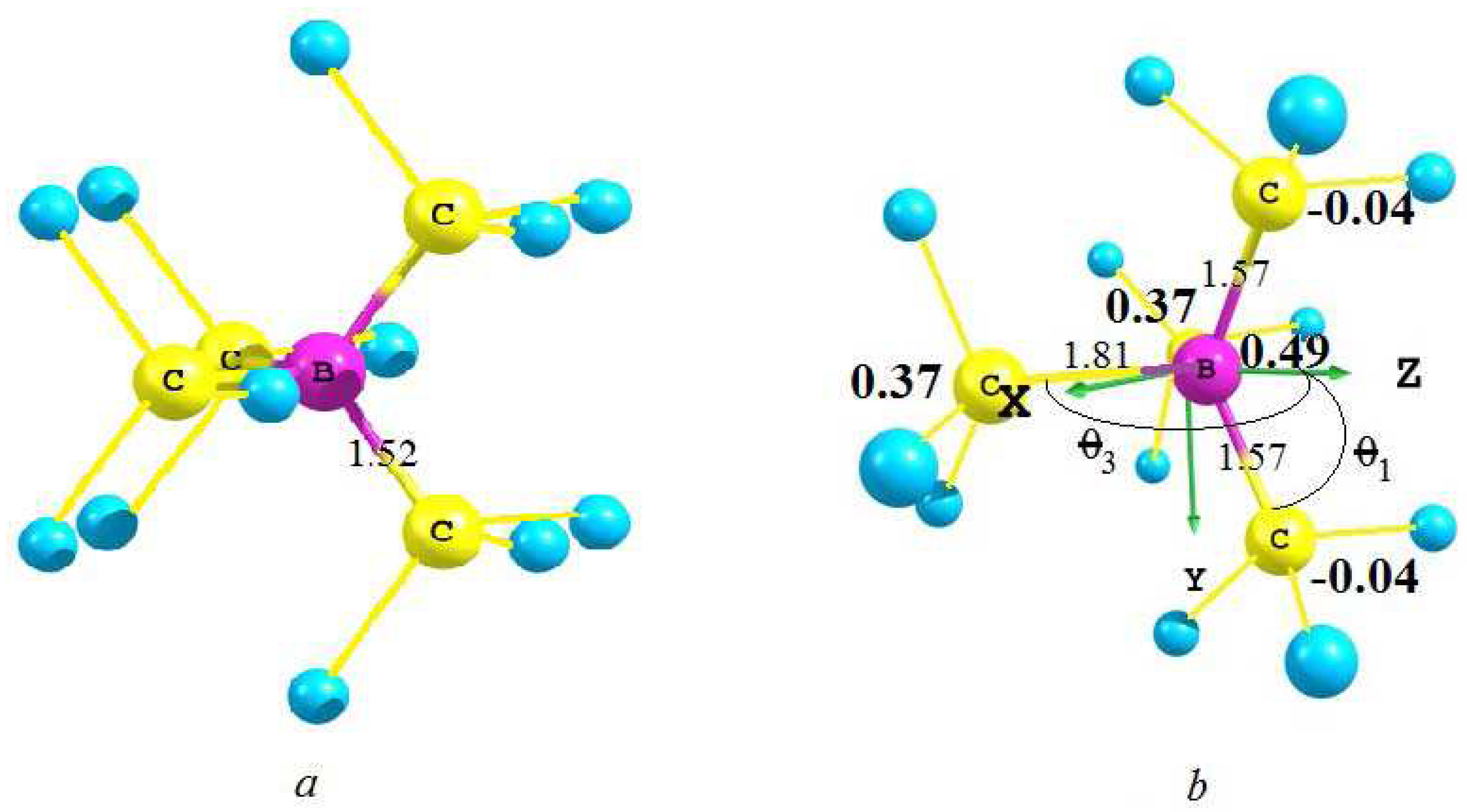
We suppose also that the electronic configuration for the principle quantum number is completely filled, and electronic states of the external atomic shell are described by unperturbed wave functions of a free atom. The initial state of the radiation defect in a diamond lattice is shown schematically in Figure 2a.
The mixed state (9) forms a chemical bond with the nearest host atoms of the lattice. We express a wave function of the initial state (9) in distinguish from the state (1) in the form of superposition with all possible spin states:
where:
is the wave function of the -state. We assume that all p-states with different projections have equal probabilities:
are the values of the total electron spin; is the appropriate spin-state vector. Spin states with different projections are considered as having equal probabilities; so coefficients in the superposition (10) satisfy the following condition:
The space part of the defect wave function in the final state must correspond to the determined value of the total electron spin S, and this can be represented in the form of the superposition of hybridized states providing a chemical bond with the lattice host atoms:
where summation is carried out over all possible directions of the chemical bond of impurity valence electrons with the nearest neighbors of the lattice,
5. Formation of the Neutral Center (A A in Si and Ge
A lifetime of exited states (1) and (10) is determined by a rate of a radiation transition in a bond state and can be calculated by using Fermi’s “golden rule”:
The interaction operator is:
where is the vector-potential of the free radiation field.
Let us consider now only the term for one electron with in the operator (14) to simplify the following calculations. In this case, matrix elements of the perturbation operator could be represented by the expression:
and:
where the indexes are .
If we direct the axis , then the other three p-states in hybridized states (6) turn out as a result of the rotation of the state in the state with a rotation moment projection equal to zero on the axes . In this case, we get the opportunity to calculate easy integrals incoming in Expressions (16) and (17):
where is the rotation operator, and the matrix elements (19) are determined by the second column of the rotation matrix:
We put in Equation (18) the obvious expressions of the matrix elements of the rotation operator (see e.g., [29]).
Without reduction of the generality of the calculations, we consider a matrix element only for the z- projection of a momentum operator. Therefore, we have:
where:
For clarity, we show some intermediate calculations. The total matrix element in Expression (14) consists of 72 different items corresponding to different matrix elements between states of the superpositions (2) and (4). However, it is enough to calculate only four of them. We give them below.
The rest of the three matrix elements are determined by the other possible sets of for the electrons with coordinates and :
It is easy to see that permutations of electrons in the superposition (5) do not change expressions for the matrix elements (24)–(27). Therefore, the number of permutations in the state (5) with similar expressions reduces the total number of items by six-times.
We get a very cumbersome expression for the arbitrary values of the parameters and . However, it is necessary to take into account that the system under consideration has a symmetry at less . In this case, the result could be essentially simplified. We examine the simplest case at first, when the system has a tetrahedral symmetry and all parameters in the hybridized states (6) are equal to each other:
If the vector lies in the plane, the angles are equal:
In the case of symmetrical structure, we get the following expressions for the matrix elements:
Adding up Expressions (30)–(32), we get:
The matrix elements for the state with are calculated by a similar way:
For the state with :
After substitution of the values o Parameters (28) and (29) and adding up Expressions (33)–(35), we have:
For the calculation of the integral , we take the appropriate wave functions of the hydrogen-like atom with an effective nuclear charge equal to . In accordance with Slater [30], an effective charge is determined as , where Z is the real nuclear charge and is a screening constant.
In a silicon crystal, an aluminum -atom Al is formed. It has the principle quantum number , and appropriate calculations for Al give the following results:
where is the Bohr radius.
In a germanium lattice, a gallium -atom Ga with the principle quantum number must be formed. The unknown value of the matrix element for Ga is equal to:
In the calculation of a transition probability per unit time, we will take into account that at least three electrons participate in the matrix element of the operator (19), and the number of spin states in Determinant (3) is :
Here, appropriates the transition frequency of a neutral radiation defect from the energy level of the corresponding free atom state on the energy level corresponding to a hybridized state in a lattice.
After integration over the wavevector of photons and averaging over all angles, we get:
where is the fine structure constant. We have substituted here the effective charge and in accordance with Slater [30].
6. Formation of Neutral Center (B C in Diamond
Formulae (16) and (17) must be modified for diamond in accordance with Equations (11) and (13) as follows:
and:
To derive a common expression now, we consider that the Z-axis does not coincide with any of the bond directions . Therefore, as for (18) and (19), we have:
Without the reduction of the generality of the calculations, we consider a matrix element only for the z- projection of a momentum operator.
where is determined by Equation (23) for .
The interaction operator (15) conserves the total spin, and we need to calculate only matrix elements for the superpositions (10) and (12) between states with equal total spins. For states with a total electron spin , the matrix elements of the interaction operator in Expression (14) are equal to zero because of the symmetry of the two-particle states (11) and (13). Therefore, contrary to calculations performed for neutral defects in Si and Ge, it is necessary to calculate matrix elements only for singlet states. Accordingly, a radiation transition in dipole approximation for triplet-states (with a maximum spin value of the (B) defect) is forbidden. Note that singlet spin states constitute only 1/4 part of all spin states under the assumption of an equal probability of a population of all spin states. This fact leads to the reduction of a total probability transition by nine-times with respect to the probability transition between triplet states.
Taking into account a local symmetry of the B C cluster, we direct axes as shown in Figure 2b and introduce the following designations: . We have, respectively, . After summation over all bonds, one obtains the expression:
We can determine superposition coefficients in (6). Taking into account the relations (8) as and, respectively, . Therefore, we have:
Here, the condition and, respectively, were used.
Finally, the matrix element (47) can be written in the form:
For the appropriate wave functions of the hydrogen-like atom with an effective nuclear charge equal to , the integral is equal to:
An effective charge for a boron atom is equal to [30].
In the calculation of the probability of a transition per unit time, we shall take into account that two electrons participate in the matrix element of the operator (15). Carrying out integration over a wavevector of photons and averaging over all angles, we obtain:
Here, corresponds to a transition frequency of the charged radiation defect from the energy level of the free ion (B) to the energy level of the hybridized (bound) state in the lattice B C.
In accordance with the matrix element (49) and the result of the matrix element (50) calculation, a configuration factor is equal to:
A transition frequency and angles for a configuration factor were calculated numerically in [28] by the quantum-chemical methods. The crystalline chemical environment of clusters in Figure 2 has been taken into account by the procedure [31] based on a passivation of unnatural valences on a border of the cluster by hydrogen atoms. The variation of the geometrical position of the H* atoms, if it is possible, ensures the stoichiometry of the charge distribution on the carbon atoms of the model CH* fragment (Figure 2a, where the B atom is substituted by the central C atom).
The initial state of the radiation (B) defect in a diamond lattice is modeled by the tetrahedral structure of Figure 2a where the central carbon atom is substituted by the B atom, and the non- equilibrium length of four B–C bonds coincides with the equilibrium length of 1.523 Å for C–C bonds found by us earlier after geometry optimization of the central structural CH* fragment. As a result of a structural relaxation, the defect transits into the final hybridized state described by the lowest in energy triplet structure of the [BCH* cluster (Figure 2b). The energy of such a transition is calculated from the difference between the total energies of levels and to be equal to 1.17 eV.
The angles in the cluster are equal to . Calculations of a spin density at the center of the cluster give the value of the superposition parameter . The effective charge for and states of the boron atom is . Substituting the calculated values into Formulas (51) and (52), we obtain a numerical estimate of the radiation transition rate of the impurity center B into a hybridized state:
The obtained value confirms the validity of the assumption on the kinetics of a charged radiation defect B thermalization reported in [24]. The hybridization rate (53) is two orders of magnitude less than the rate of a non-hybridized charged center formation.
The hybridized charged center (B) quickly, during characteristic lattice times, transfers into a neutral state. Therefore, the neutralization time of a charged defect formed by a negative muon in a diamond lattice is determined by the value of (53), and at least two order higher than that for silicon and germanium (40).
7. Formation of an Ionized Acceptor Center
In this section, we will consider the process of an electron capture on the neutral radiation defect with totally restored chemical bonds and the formation of an acceptor center in the ionized state.
According to our cluster calculations, the neutral B)C defect has symmetry and creates the substantial electric dipole moment, which is equal to 1.08D, in a diamond lattice. Here, D is Debye, the unit of an electric dipole moment in the atomic system of units (DCGSE). The dipole moment is directed along the symmetry axis. Therefore, we can suppose that any neutral cluster of a type A) A in crystals with a diamond structure possesses an electric dipole moment of the order of 1D.
This electric dipole moment gives rise to an interaction necessary to capture a lattice electron and the form of an ionized acceptor center. The neutral center A has unsaturated chemical bonds because a crystal lattice turns out to be deformed. This deformation is a reason to change a phonon spectrum and the local phonon mode appearance. Chemical bounds are saturated after the missing electron capture. The new cluster is an ionized acceptor center and possesses a local crystal symmetry. When the ionized acceptor center is formed, an appropriate phonon of the local mode is radiated, and crystal deformations disappear. Therefore, the problem is very similar to the problem of the thermalization of molecular ions in molecular crystals and cryocrystals of noble atoms (see e.g., [32,33,34]). An exact solution of the problem taking into account a crystal symmetry is scarcely possible. However, qualitative estimations can be obtained in some approximations [35,36].
7.1. Effective Hamiltonian and Interaction Operator
Detailed calculations of an ionized acceptor center formation in diamond, silicon and germanium were carried out in [35,36], and here, we will present the main results. The electric dipole moment creates a scalar potential, and the interaction energy with lattice electrons is , where is a dielectric penetration. Therefore, taking into account the displacement () and neglecting the changing of the denominator of the potential, we can write an electron-phonon interaction operator:
The operator of radial displacements can be determined in the approach of an isotropic elastic media. For this reason, we need to study vibrations of a sphere at the center of which is placed an electric dipolar moment . This dipolar moment creates an electric induction , and a displacement vector satisfies the following equation:
where is the longitudinal sound velocity, is the dielectric susceptibility and , is the density of a media.
To solve Equation (55), we will take into account only radial vibrations of a deformed crystal lattice with respect to the center of the sphere. The center of this sphere coincides with our radiation defect. Therefore, we can introduce as usual for problems with central symmetry a radial displacement . In this case, we have the more simple equation for :
where is the second derivative on the radial variable r. Making the one-dimensional Fourier transformation for the function :
we obtain a dispersion relation in a long wavelength approximation:
where is the radius of the first coordination sphere. More detailed calculations are represented in Appendix A.
The numerical estimates for the frequency in diamond, silicon and germanium crystals are presented in Table 1 (the parameters oft the crystals were taken from [37,38]). Since a dipole moment d is considered as an unknown parameter, the numerical estimates are presented in units of Debye.
Now, we can construct an effective Hamiltonian describing the radial vibrations of a lattice and determine the operator of radial displacements in Operator (54). Consider radial vibrations in a sphere with the radius with boundary conditions . Keeping a dependence on time t, we need to use discrete Fourier amplitudes instead of Equation (57):
where .
Therefore, and are generalized coordinates and the momentum of the system under consideration, respectively. The effective Hamiltonian for a system of independent oscillators can be written as:
Here,
and the dimensionless generalized momentum and coordinate are defined as usual:
while the units of the generalized momentum and coordinate are equal to:
Introducing, as usual, the annihilation and creation operators:
we obtain the operator of radial displacements of a lattice, which must be substituted in Equation (54), in the form:
It is easy to see that the interaction operator (54) has a strong singularity at , which leads to the divergence of matrix elements. However, Operator (54) is obtained in a dipolar approximation; its expression is valid for respectively large values of the radius vector and is not applicable at . In this case, as usual (see e.g., [39]), the potential is taken as constant at , where is a certain characteristic distance, i.e.,
In our case, we can take , where is the length of chemical bonds in the lattice.
7.2. Electron Capture Rate
The probability of electron capture per unit time can be calculated with the well-known Fermi golden rule:
We will consider a case of low temperature, and the initial state corresponds to the free electron in the valence band with the wave-vector and the absence of exited radial phonons. The final state is determined by the captured electron to the or hybridized state of the cluster and by the excitation of the radial phonon with the wavevector :
Here, and 4 for C, Si and Ge, respectively. Equation (66) takes into account that all electrons having wavevectors in the interval from to can be captured by the cluster.
The volume element of the final states in the case of one-dimensional motion is equal to:
where is the element of the solid angle into which a phonon is emitted. The energies of the initial and final states are:
is the effective mass of the electron. To obtain numerical results, the ionization energy of the cluster (acceptor) is taken for .
Integration of (66) over k gives:
where a vector of the final state takes into account electron states only, and according to Equation (65),
Here:
For the further analysis, it is convenient to introduce the dimensionless parameters and variables:
where and 4 for C, Si and Ge, respectively. The estimated characteristic parameters for considered crystals are summarized in Table 2.
All considered crystals are anisotropic, and the sound velocity in the dispersion relation (58) depends on the direction of a phonon propagation. To take this into account, we will use, as usual, the average value of the longitudinal velocity of sound , neglecting the effects of anisotropy.
We define a characteristic frequency:
and corresponding dimensionless frequencies and . Taking into account the dispersion relation of the radial phonons (58), we can write the electron capture rate in the form:
where:
The dimensionless matrix element is determined by Function (68):
Equation (72) shows that the electron can be captured both in s- and p-states of the hybridized state of the cluster. As was shown in [36], the capture rate to the p-state is approximately two orders less than the capture rate to s-state . Therefore, in the following, we can consider the electron capture to the s-state. In this case, the matrix element (74) is given by the expression:
where and are the real and imaginary parts of the matrix element, respectively. Finally, the capture rate (72) has the form:
Obtained Formula (76) determines the formation rate of the ionized acceptor center through the capture of the electron of the medium on the neutral radiation defect induced by the negative muon or pion in crystals. Analytical expressions depend on well-known characteristic parameters of the medium except for two parameters of the cluster, namely, the electric dipolar moment d and the parameter in Equation (65). The dependence on d of the integral in Equation (75) is weak and can assume that . Unfortunately, the dependence of the results on the parameter is more critical, because the matrix elements exponentially depend on the lower integration limit. Nevertheless, the parameter cannot be smaller than the length of the chemical bound in the lattice. We can determine the upper limit also , the radius of the first coordination sphere.
Numerical calculation were performed for several different values of the uncertain parameters d and . The results are summarized in Table 3.
According to the obtained results in the considered range of the uncertain parameters and d, the spread of the estimates of the capture rates is about two orders of magnitude and seems at first unsatisfactory. However, it is not surprising because both the dipole approximation and the dispersion relation for the radial phonons (58) are quite rough for . Nevertheless, the considered interaction mechanism is fairly justified and describes the process of the electron capture on the neutral defect of the lattice with the formation of the ionized state of the acceptor center.
8. Discussion
We have considered the total process of an acceptor center formation in crystals with the diamond structure, which appears as a radiation defect induced by negative pions or muons. It was shown that the evolution of this kind of radiation defects can be divided into two physically different stages. At the first stage, the negatively-charged particle is stopped in the crystal and captured by a nucleus with the charge Z (in the case of ) or at the K-shell of a muonic atom (in the case of ). Both negative pions and muons create a host nucleus with an effective charge . This strongly-charged center interacts with trace electrons and captures them. This stage of radiation defect neutralization exists because of Coulomb interaction. Numerical calculations show that this stage of neutralization strongly differs in diamond and other crystals. Namely, the radiation defect is completely neutralized in Si and Ge for a relatively short time s. In diamond, this radiation defect can be completely neutralized for a long time s.
The second stage of evolution of this radiation defect is connected with restoration of chemical bonds with the lattice as the first step and formation of an appropriate acceptor center as the final step. Chemical bonds in Si and Ge are restored for neutral radiation defects and in C chemical bonds can be formed for a single-fold charged center. Formation of a chemically-bound radiation defect is accompanied with sufficiently large energy emission. Therefore, the process of chemical bonds’ formation can be described with the help of radiation transition. Our estimates gave rather a long time for this step: s for Si and s for Ge. Charged radiation defect in C forms chemical bonds very quickly: s. We can see that this time is many orders shorter than . Therefore, the radiation defect in diamond is neutralized in the chemically-bound state. This time cannot be strictly estimated, but we can suppose that it is determined by characteristic electronic times in the lattice and must be of the order of s. We can conclude that the first step of the formation of a chemically-bound neutral radiation defect is approximately two orders shorter in diamond with respect to silicon and germanium.
The second step finishes the formation of an acceptor center in the ionized state. This step is similar in all of the above-mentioned crystals, but very complicated for obtaining good quantitative results. We can see that the chemically-bound neutral radiation defect is a cluster with unsaturated chemical bonds. This unsaturated chemical bond can be saturated if an electron of a valence band of the crystal is captured by the cluster. What kind of interaction gives an opportunity to capture a missing electron? The neutral cluster possesses a relatively large electric dipole moment, which interacts with lattice electrons. This interaction can be qualitatively described in the dipolar approximation. Our analytical and numerical calculations show that:
The total time for the acceptor center formation in the ionized state as a result of a radiation defect induced by negative pions and muons is the sum of times for all steps:
and is determined by the longest item. The final step is slower with respect to the first two steps, and we can conclude that the formation time of the ionized acceptor center is the shortest for diamond (≤ s) and the longest for silicon (≤ s). These values are comparable with characteristic times in semiconductor devices.
9. Conclusions
The obtained results will be useful both for SR experiments and research of different radiation defects in semiconductors. The considered approach can be applied to crystals with the sphalerite-type structure (AB semiconductors, e.g., GaAs, InSb, CdS), which are widely used in electronic devices. Unfortunately, these crystals are more complicated for analysis because of the large variety of possible impurity centers. In addition, the model of chemical bonds must be modified for some calculations.
Acknowledgments
I acknowledge my colleagues Leonid E. Fedichkin and Leonid P. Sukhanov for fruitful discussions. This work is supported by the Ministry of Education and Science of the Russian Federation 16.7162.2017/8.9.
Conflicts of Interest
The authors declare no conflict of interest.
Appendix A
The function can be represented in the form of the “one-dimensional” Fourier-transform:
An integral equation can be obtained for the Fourier amplitude given by Equation (A1) taking into account that the expression for the force in Equation (54) is valid for , where is the radius of the first coordination sphere, i.e.,
After passage of the Fourier amplitude on the right-hand side of Equation (A3), this equation is reduced to the form:
Another serious simplification should be done in Equation (A4). The maximum contribution to the second integral comes from wavevectors . For this reason, the term can be neglected, and the Fourier amplitude can be taken at the point k. In particular, this means that that the main contribution to the integral comes from the values . Correspondingly, in the accepted approximation, the integral on the right-hand side can be modified to the form:
After that, the simple dispersion relation (58) is obtained.
References
- Honniger, F.; Fretwurst, E.; Lindstrom, G. DLTS measurements of radiation induced defects in epitaxial an MCz silicon detectors. Nucl. Instrum. Methods Phys. Res. Sect. A 2007, 583, 104–108. [Google Scholar] [CrossRef]
- Grilj, V.; Skukan, N.; Jakšić, M. Irradiation if thin diamond detectors and radiation hardness tests using MeV protons. Nucl. Instrum. Methods Phys. Res. Sect. B 2013, 306, 191–194. [Google Scholar] [CrossRef]
- Guthoff, M.; de Boer, W.; Muller, S. Simulation of beam induced lattice defects of diamond detectors using FLUKA. Nucl. Instrum. Methods Phys. Res. Sect. A 2014, 735, 223–228. [Google Scholar] [CrossRef]
- Sato, Y.; Shimaoka, T.; Kaneko, J.H. Radiation hardness of a single crystal CVD diamond detector for MeV energy protons. Nucl. Instrum. Methods Phys. Res. Sect. A 2015, 784, 147–150. [Google Scholar] [CrossRef]
- Grilj, V.; Skukan, N.; Jakšić, M. The evaluation of radiation damage parameter for CVD diamond. Nucl. Instrum. Methods Phys. Res. Sect. B 2016, 372, 161–164. [Google Scholar] [CrossRef]
- Makgato, T.H.; Sideras-Haddad, E.; Ramos, M.A. Magnetic properties of point defects in proton irradiated diamond. J. Magn. Magn. Mater. 2016, 413, 76–80. [Google Scholar] [CrossRef]
- Vins, V.G. New radiation induced defects in HPHT synthetic diamonds. Diam. Relat. Mater. 2005, 14, 364–368. [Google Scholar] [CrossRef]
- Dresselhaus, M.S.; Kalish, R. Ion implantation in Diamond, Graphite and Related Materials; Springer: Berlin, Germany, 1992. [Google Scholar]
- Vonsovsky, S.V. Magnetizm of Microparticles; Nauka: Moscow, Russia, 1973; pp. 1–197. (In Russian) [Google Scholar]
- Smilga, V.P.; Belousov, Y.M. The Muon Method in Science; Nova Science: New York, NY, USA, 1994; pp. 1–420. [Google Scholar]
- Waisenberg, A.O. Mu-Meson; Nauka: Moscow, Russia, 1964; pp. 1–400. (In Russian) [Google Scholar]
- Dzhuraev, A.A.; Evseev, V.S. Mechanism of mu-meson depolarization in molecular condensed media. Sov. Phys. JETP 1972, 35, 615–819. [Google Scholar]
- Dzhuraev, A.A.; Evseev, V.S.; Myasishcheva, G.G. Depolarization of negative muons in solids. Sov. Phys. JETP 1972, 35, 748–752. [Google Scholar]
- Dzhuraev, A.A.; Evseev, V.S. Depolarization of negative muons in condensed molecular media. Sov. Phys. JETP 1974, 39, 207–211. [Google Scholar]
- Gorelkin, V.N.; Smilga, V.P. On the theory of precession of the polarization vector of μ−-mesons in mu-nucleonic atoms. Sov. Phys. JETP 1974, 66, 586–591. [Google Scholar]
- Gorelkin, V.N.; Grebinnik, V.G.; Gritsaj, K.I. μSR-study of the behavior of impurity atoms in silicon. Phys. At. Nucl. 1993, 56, 1316–1319. [Google Scholar]
- Mamedov, T.N.; Duginov, V.N.; Grebinnik, V.G. Investigation of the behavior of the impurity atoms in Si by μSR-method. Hyperfine Interact. 1994, 86, 717–722. [Google Scholar] [CrossRef]
- Mamedov, T.N.; Chaplygin, I.L.; Duginov, V.N. Anomalous frequency shift of negative muon spin precession in n-type silicon. Hyperfine Interact. 1997, 105, 345–349. [Google Scholar] [CrossRef]
- Mamedov, T.N.; Gritsaj, K.I.; Stoykov, A.V. μ−SR investigations in silicon. Phys. B 2000, 289–290, 574–577. [Google Scholar] [CrossRef]
- Mamedov, T.N. Study of Boron Acseptor Center in Synthetic Diamond by μSR-Technique; JINR Preprint P14-2007-12; JINR: Dubna, Russia, 2007. (In Russian) [Google Scholar]
- Mamedov, T.N.; Baturin, A.S.; Blank, V.D. Non-equilibrium charge carrier dynamics in synthetic diamond studied by μSR-method. Diam. Relat. Mater. 2008, 17, 1221–1224. [Google Scholar] [CrossRef]
- Mamedov, T.N.; Baturin, A.S.; Gritsaj, K.I. Muonic atom as an acceptor centre in diamond. J. Phys. Conf. Ser. 2014, 551, 012046. [Google Scholar] [CrossRef]
- Baturin, A.S.; Gorelkin, V.N.; Mamedov, T.N.; Soloviev, V.R. Absolute negative mobility of charge carriers in diamond and interpretation of μSR experiments. Phys. B 2006, 374–375, 340–346. [Google Scholar] [CrossRef]
- Antipov, S.A.; Belousov, Y.M.; Soloviev, V.R. Dynamics of charge carriers at the place of the formation of a muonic atom in diamond and silicon. JETP 2012, 115, 866–875. [Google Scholar] [CrossRef]
- Belousov, Y.M. Formation of radiation defect induced by negative muons in crystals with diamond structure. J. Phys. Conf. Ser. 2012, 343, 012013. [Google Scholar] [CrossRef]
- Pauling, L. Natureof the Chemical Bond, 3rd ed.; Cornell University Press: Ithaca, NY, USA, 1960. [Google Scholar]
- Coulson, C.A. Valence; Oxford University Press: Oxford, UK, 1961. [Google Scholar]
- Belousov, Y.M.; Sukhanov, L.P. Formation of chemically bound positively charged radiation defect induced by negative muon in diamond crystals. Diam. Relat. Mater. 2015, 58, 10–15. [Google Scholar] [CrossRef]
- Landau, L.D.; Lifshitz, E.M. Quantum Mechanics. Nonrelativistic Theory, 3rd ed.; Pergamon: Oxford, UK; New York, NY, USA, 1977. [Google Scholar]
- Slater, J.C. Atomic Shielding Constants. Phys. Rev. 1930, 36, 57–64. [Google Scholar] [CrossRef]
- Groshev, G.E.; Sukhanov, L.P. Quantum-chemical cluster models of the Si(111)/SiO2 interface. Theor. Exp. Chem. 1990, 26, 268–275. (In Russian) [Google Scholar] [CrossRef]
- Belousov, Y.M.; Smilga, V.P. Theory of muon spin relaxation in condensed phases of hydrogen isotopes. JETP 1994, 79, 811–818. [Google Scholar]
- Belousov, Y.M. Theoretical description of the muon spin depolarization in the crystalline phase of 3He. JETP 2007, 104, 215–229. [Google Scholar] [CrossRef]
- Belousov, Y.M.; Smilga, V.P. Theory of muon spin relaxation in condensed phases of hydrogen isotopes. Hyperfine Interact. 1997, 106, 19–25. [Google Scholar] [CrossRef]
- Belousov, Y.M. Process of an acceptor center μB− formation in diamond crystals. J. Phys. Conf. Ser. 2014, 551, 012047. [Google Scholar] [CrossRef]
- Belousov, Y.M. Process of negative-muon-induced formation of an ionized acceptor center (μA)− in crystals with diamond structure. JETP 2016, 123, 1160–1169. [Google Scholar] [CrossRef]
- Madelung, O. Semiconductors—Basic Data., 3rd ed.; Springer: Berlin/Heidelberg, Germany, 2004. [Google Scholar]
- Adachi, S. Properties of Group-IV, III-V and II-VI Semiconductors. Wiley Series in Materials for Electronic & Optoelectronic Applications; John Wiley & Sons: Chichester, UK, 2005. [Google Scholar]
- Abakumov, V.N.; Perel, V.I.; Yasievich, I.N. Nonradiative Recombination in Semiconductors; SPb.Institute of Nuclear Physics RAS: Amsterdam, The Netherlands, 1997. [Google Scholar]
- Lax, M. Cascade capture of electron in solids. Phys. Rev. 1960, 119, 1502–1523. [Google Scholar] [CrossRef]
- Abakumov, V.N.; Yasievich, I.N. Cross section for recombination of an electron with a positively charged center in a semiconductor. Sov. Phys. JETP 1976, 44, 345–349. [Google Scholar]
Figure 1.
Radiation defect Al state in a silicon lattice: (a) all bonds with host atoms are broken in the initial state, and the defect state is determined by the “mixed” function ; (b) three electrons of the impurity form chemical bonds with host atoms in the final state, and an unsaturated (broken) bond is equiprobable for four nearest neighbors of the cluster (AlSi.
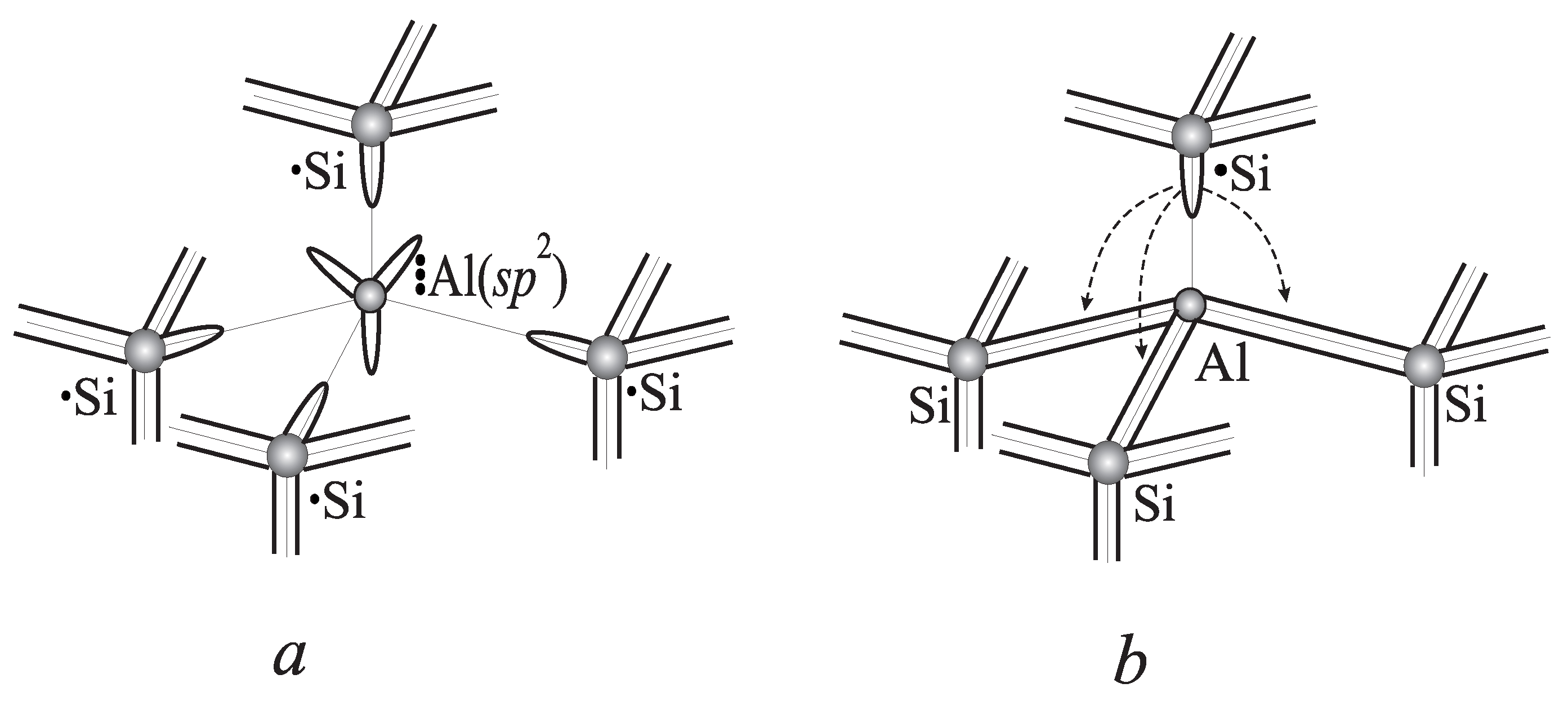
Figure 2.
Structure of the radiation (B) defect in a diamond lattice: (a) the BC cluster has a symmetry in the initial triplet state; (b) it has a lower symmetry with angles and in the final triplet state. The internuclear distances are given in Å. The spin densities on atoms are marked by bold type.

Table 1.
Physical parameters of the C, Si and Ge crystals and the estimate of the frequency .
| Crystal | Density , g cm | cm | Dielectric Constant | s | Ionization Energy of the Acceptor, eV |
|---|---|---|---|---|---|
| Diamond | 3.51 | 3.57 | 5.75 | 8.1 d | B, 0.37 |
| Silicon | 2.33 | 5.43 | 11.97 | 1.4 d | Al, 0.069 |
| Germanium | 5.323 | 5.66 | 16.0 | 0.66 d | Ga, 0.011 |
Table 2.
Characteristic parameters estimated for C, Si and Ge.
| Crystal | , cm | , c | , cm | , cm | ||||
|---|---|---|---|---|---|---|---|---|
| C | 1.54 | 2.6 | 3.78 | 3.32 | 3.1 | 0.48 | 4.2 | 15.9 |
| Si | 2.34 | 3.5 | 5.15 | 1.05 | 1.34 | 0.31 | 1.18 | 2.78 |
| Ge | 2.44 | 5.0 | 5.75 | 1.24 | 0.54 | 0.13 | 0.32 | 0.77 |
Table 3.
Estimate of the formation rate of ionized acceptor centers in the C, Si and Ge crystals.
| d | , C | , C s | , Si | , Si s | , Ge | , Ge s |
|---|---|---|---|---|---|---|
| 1.0 | 3.78 | 22.0 | 5.12 | 0.71 | 5.76 | 14.3 |
| 0.5 | 3.78 | 5.9 | 5.12 | 0.19 | 5.76 | 3.8 |
| 0.2 | 3.78 | 0.98 | 5.12 | 0.034 | 5.76 | 0.65 |
| 1.0 | 5.5 | 2.2 | 7.5 | 0.095 | 7.5 | 2.4 |
| 0.5 | 5.5 | 0.58 | 7.5 | 0.024 | 7.5 | 0.64 |
| 0.2 | 5.5 | 0.09 | 7.5 | 2.6 | 7.5 | 0.11 |
© 2017 by the author. Licensee MDPI, Basel, Switzerland. This article is an open access article distributed under the terms and conditions of the Creative Commons Attribution (CC BY) license (http://creativecommons.org/licenses/by/4.0/).
Share and Cite
MDPI and ACS Style
Belousov, Y.M. Evolution in Time of Radiation Defects Induced by Negative Pions and Muons in Crystals with a Diamond Structure. Crystals 2017, 7, 174. https://doi.org/10.3390/cryst7060174
AMA Style
Belousov YM. Evolution in Time of Radiation Defects Induced by Negative Pions and Muons in Crystals with a Diamond Structure. Crystals. 2017; 7(6):174. https://doi.org/10.3390/cryst7060174
Chicago/Turabian StyleBelousov, Yury M. 2017. "Evolution in Time of Radiation Defects Induced by Negative Pions and Muons in Crystals with a Diamond Structure" Crystals 7, no. 6: 174. https://doi.org/10.3390/cryst7060174
Note that from the first issue of 2016, this journal uses article numbers instead of page numbers. See further details here.