
Microstructure and Electrical Properties of Fe,Cu Substituted (Co,Mn)3O4 Thin Films


1
Faculty of Electronics, Telecommunications and Informatics, Gdansk University of Technology, ul. G. Narutowicza 11/12, 80-233 Gdansk, Poland
2
Department of Energy Conversion and Storage, Technical University of Denmark, Risø Campus, Frederiksborgvej 399, 4000 Roskilde, Denmark
*
Author to whom correspondence should be addressed.
Crystals 2017, 7(7), 185; https://doi.org/10.3390/cryst7070185
Submission received: 19 May 2017
/
Revised: 14 June 2017
/
Accepted: 17 June 2017
/
Published: 23 June 2017
(This article belongs to the Special Issue Crystal Structure of Electroceramics)
Abstract
:In this work, thin films (~1000 nm) of a pure MnCo2O4 spinel together with its partially substituted derivatives (MnCo1.6Cu0.2Fe0.2O4, MnCo1.6Cu0.4O4, MnCo1.6Fe0.4O4) were prepared by spray pyrolysis and were evaluated for electrical conductivity. Doping by Cu increases the electrical conductivity, whereas doping by Fe decreases the conductivity. For Cu containing samples, rapid grain growth occurs and these samples develop cracks due to a potentially too high thermal expansion coefficient mismatch to the support. Samples doped with both Cu and Fe show high electrical conductivity, normal grain growth and no cracks. By co-doping the Mn, Co spinel with both Cu and Fe, its properties can be tailored to reach a desired thermal expansion coefficient/electrical conductivity value.
1. Introduction
Ceramic materials are important in engineering. Many future efficient energy conversion and storage technologies depend on the development of new electroceramic materials with desired and tailored properties [1,2,3,4,5]. Materials based on MnCo2O4 are interesting for a broad range of applications, from room temperature to high temperatures (800 °C). They can be used in Li-ion battery electrodes [6,7], electrochemical supercapacitors [8] and as coating materials for steel interconnects for fuel cells [9,10,11]. The microstructure and the composition of the spinel strongly affect its performance and applicability in a specific technology. In recent years, doping of the spinel by either Fe or Cu has been pursued in order to increase its electrical conductivity, enhance sintering and possibly alter the thermal expansion coefficient [12,13]. Only very recently has simultaneous substitution by both Fe and Cu been reported (on bulk samples) [13].
Manganese cobalt spinel is a preferred material for high temperature protective coatings for steel interconnects for Solid Oxide Fuel/Electrolysis stacks [14]. Its high electrical conductivity and the low mobility of chromium in the material are two important qualifying factors [15]. For high temperature protective coatings, thicknesses > 10 µm are typically used, whereas in applications like supercapacitors and Li-ion batteries, thin films or composites are typically used.
Electrical conductivity of thin films of several materials showed interesting behavior. Effects like ionic conductivity and activation energy dependent on the grain size have been reported [16]. For example, Rupp et al. have studied an ionically (O2−) conducting CGO (cerium-gadolinium oxide) and YSZ (yttria-stabilized zirconia) thin films deposited by spray pyrolysis [17,18]. These studies have revealed very interesting properties of thin films prepared by the low temperature spray pyrolysis process.
Spray pyrolysis is a solution based deposition method, in which liquids are deposited on a heated substrate via droplets from a pressurized atomizer. In comparison to other solution based deposition methods, e.g., spin coating, thermal decomposition of the liquid precursor occur directly on the surface during the deposition process [19,20,21,22]. Therefore, spray pyrolysis is a cost and time effective method, well suited for fabrication of thin nanocrystalline films [19]. An important advantage of the solution based methods is their easy ability to modify the chemical composition of the desired products by adding dopants to the liquid precursor.
In this work, MnCo2O4 spinel and Cu/Fe substituted derivatives (MnCo1.6Cu0.4O4, MnCo1.6Fe0.4O4, MnCo1.6Cu0.2Fe0.2O4) are deposited in the form of thin (~1 µm) films by spray pyrolysis. Sapphire was used as a substrate and the in-plane electrical properties and microstructure of the films were characterized as a function of temperature up to 800 °C.
2. Materials and Methods
Four kinds of polymeric precursor solutions were prepared in order to create a dense layer on a 500 µm thick c-plane sapphire substrate by the spray pyrolysis method. The concentration of cations in each precursor was fixed at 0.2 mol/L. For precursor preparation, Mn(NO3)2·4H2O, Co(NO3)2·6H2O, Cu(NO3)2·3H2O and Fe(NO3)3·9H2O nitrate salts were used. For MnCo2O4, MnCo1.6Cu0.4O4, MnCo1.6Fe0.4O4 and MnCo1.6Cu0.2Fe0.2O4 nitrate salts were mixed in a stoichiometric ratio 1:2, 1:1.6:0.4, 1:1.6:0.4 and 1:1.6:0.2:0.2, respectively. Salts were dissolved in a mixture of deionized water, diethylene glycol and tetraethylene glycol (1:1:8 vol % respectively). For spray pyrolysis, the following deposition parameters were used: hot plate temperature −390 °C, precursor flow rate −1 mL/h, nozzle-surface distance −600 mm, air pressure −2 bars. For the desired 1 µm layer thickness, 20 mL of the precursor was used. For each composition, two samples with an approximate dimension of 1 × 1 cm2 were prepared. One has been used for the electrical conductivity study, the second for the in-situ high temperature c.
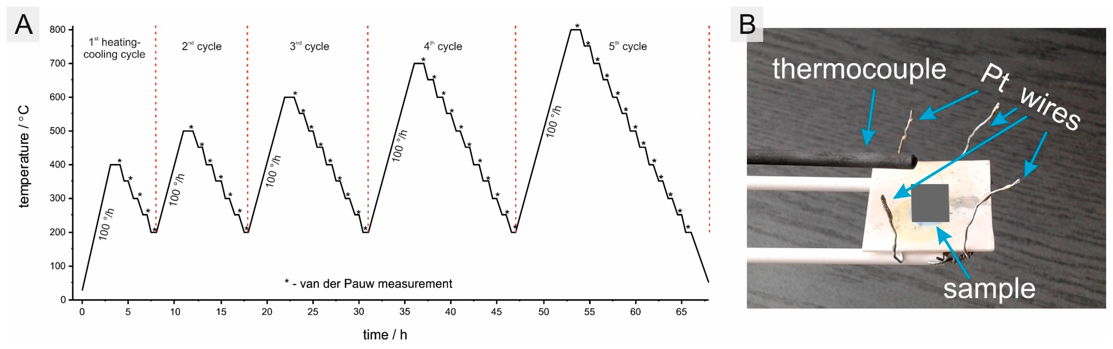
The deposited layers were characterized for their electrical conductivity using the van der Pauw method. To get more information about crystallization and electrical conductivity, five heating-cooling cycles were followed, as presented in Figure 1. In each cycle, the samples were heated with a rate of 100 °C/h until the maximum designed temperature was reached. Every cycle had different maximum temperatures starting with 400 °C for the 1st cycle, and 500 °C, 600 °C, 700 °C and 800 °C for the subsequent cycles. For each cycle, the temperature was held at maximum for 1 h. The data were collected from the highest temperature of the cycle and at hold during cooling down to 200 °C at every 25 °C.
For microstructural analysis of the layers, scanning electron microscope (SEM) with energy dispersive spectroscopy (EDS) and X-ray diffractometry (XRD) were used. A Hitachi TM3000 with Bruker Quantax 70 and a Zeiss Supra 35 FEG-SEM were used for characterization of both surfaces and fracture cross-sections. For XRD analysis, a Bruker D8 Advance with CuKα radiation was used. Characterization in both a standard 2θ configuration and in a grazing incidence mode were carried out. In-situ high temperature XRD measurements were carried out using an MRI heating stage based on a Pt-Rh heating element. XRD patterns were used for phase identification, determination of the crystallite size and crystal structure.
The crystallite size was calculated according to the Scherrer formula and the influence of temperature was evaluated by the procedure presented in [18]. The following equation has been used:
where: The symbols have the following meaning: d—crystallite size, K—shape factor, taken as 0.94, λ—X-ray wavelength, β—broadening at FWHM, θ—Bragg angle.
As the coatings were very thin and deposited on a sapphire substrate, Rietveld refining of the unit cell was not successful. Instead, for qualitative description, a simple approach of calculation of the lattice parameter of the cubic crystal lattice was used. Based on the position of the observed diffraction peaks in the XRD pattern, the lattice parameter was calculated from [18].
where: A—lattice parameter (Å); h, k, l—the Miller indices of the considered Bragg reflection θ, λ—X-ray wavelength (Å).
3. Results and Discussion
3.1. Analysis of the Produced Coatings
Scanning electron microscopy images of the as-prepared MnCo1.6Fe0.4O4 coatings are shown in Figure 2A,B at two different magnifications (500× and 10,000×). The surfaces of other coatings looked very similar. Due to the low processing temperature of the deposition process (~380 °C), no characteristic grain features are visible by the SEM. The coatings are continuous, they cover the surface well and no cracks nor defects are detected. The chemical compositions of the coatings have been evaluated by the EDS analysis at a low magnification (500×) to average over a large area. The EDS spectra show a presence of Mn, Co and the respective dopants, Cu and/or Fe, as illustrated in Figure 2C–F. Calculated compositions are summarized in Table 1. XRD patterns of the as-produced coatings are shown in Figure 2G. Measurements have been performed in a grazing incidence (GI) mode at an x-ray source angle of 1.5° to avoid a strong signal from the sapphire substrate. Diffraction patterns reveal broad peaks due to small crystallites and especially for the pure MnCo2O4 show possible presence of some amorphous phase (broad peak around 28°). Even at this relatively low processing temperature of ~380 °C, a cubic spinel phase has crystallized. For reference, positions of the peaks according to JCPDS-ICDD card number 23-1237 are also plotted in Figure 2G. No preferred orientation of the as-deposited film can be detected, as the intensities of the respective peaks seem to resemble the reference pattern.
The chemical composition of the coatings (determined from the EDS analysis), given in Table 1, agrees with the desired stoichiometry, though a slightly higher B atom content (in an AB2O4 structure nomenclature) is observed (~2.2 instead of the expected 2). This difference from the desired stoichiometry, noticed in all samples, might be due to a different cation content in the used nitrate salt source. Higher Co content can be tolerated as it should help to stabilize the cubic phase, as phases with a lower Co content (<2) can separate into a mixture of tetragonal Mn2CoO4 and cubic MnCo2O4 spinel [23]. Based on the cation content and assuming (based on the XRD) the existence of only the pure spinel phase, the experimentally determined stoichiometry of the spinel has been calculated.
3.2. Electrical Characterization
The as-produced coatings have been characterized electrically following the temperature profile shown in Figure 1. With each consecutive measurement, the samples have been held at maximum temperature for 1 h and then the electrical conductivity has been measured during cooling. Measurement/temperature profile has been selected to check the possible influence of crystallization, crystallite/grain growth on electrical conductivity. Recorded conductivity values are presented in an Arrhenius type plots for the four samples in Figure 3A–D.
With an initial increase in the temperature from 400 °C (~deposition temperature) to 500 °C and to 600 °C, conductivity increases for all samples. The least increase was observed for the unmodified spinel, where electrical conductivity values do not change for exposures of 400 °C and 500 °C.
Between 500 °C and 400 °C, a change in slope of the conductivity curves is observed. These effects have been reported previously for similar spinel compositions [11,24]. One possible explanation is a change in the prevailing conduction mechanism. Typically, at low temperatures, grain boundaries are considered more conductive than grains and at high temperatures, grains contribute more.
It is interesting to note, that for the exposure temperatures higher than 700 °C, a drop in electrical conductivity occurs. This happens to MCO, MCO/Fe and MCO/CuFe samples. So the maximum electrical conductivity is achieved for layers processed at ~700 °C.
Increase and change of the electrical conductivity of the layers can be due to several factors. The deposition of the layers has been performed at ~390 °C and subsequently, the samples have been evaluated by XRD and measured electrically. As evidenced by the XRD, even at this low temperature, a crystalline phase is obtained for all samples. Clearly, for the pure spinel, some amorphous phase is still present. This might be possible also for the other samples, though this is not seen in the XRD spectra.
One possibility that may account for the increase of conductivity is an increase in the degree of crystallization of the layer. The amount of the well conducting crystalline phase increases with temperature (assuming that the amorphous phase would have a lower/negligible conductivity). However, as the slope of the electrical conductivity (activation energy) curves do not change much for the samples processed at both high and low temperatures, it might be assumed that the crystalline phase (grains plus grain boundaries) has been already continuous at low temperatures. Therefore, an observed 3–4 fold increase in the electrical conductivity cannot be simply explained by a change in the ratio of the crystalline to the amorphous phase. Therefore, the main mechanism responsible for the changes of the total measured electronic conductivities might be the change of the size and thus the number of crystallites, grains and grain boundaries. The total electronic conductivity is determined by both the grain and grain boundaries contribution (σG and σGB), with typically different thermal activation. For the low exposure temperatures, with small grains, the ratio of the number (or volume part) of grain boundaries to grains would be high and with increasing temperature it decreases. This seems to be the dominating mechanism and will be studied further in future works.
For the MCO/Cu layer, some irregularities in the curves are observed, especially during the measurement with the maximum temperature of 700 °C. As will be described in more detail later, this layer had cracked and thus these results should be taken with caution.
As already mentioned, a complex behavior of the evolution of the conductivity vs. the temperature is observed for higher temperatures. Maximum conductivity values at 400 °C, 500 °C and 600 °C plotted as a function of the maximum exposure temperature are presented in Figure 4.
Figure 4 shows that layers containing Cu have roughly 4 times higher conductivity than the samples without. Also, an interesting maximum electrical conductivity for samples treated at 700 °C can be observed. It is only in the case of the MCO/Cu sample that a different trend is observed, possibly due to cracking. The highest overall electrical conductivity is found for the MCO/Cu sample. However, in this case, the conductivity values become irregular for temperatures higher than 600 °C, most likely due to the evolution of cracks in the film. The layer containing both the Cu and Fe also shows high electrical conductivity, whereas addition of Fe alone decreases the electrical conductivity.
From the observed temperature dependences of the electrical conductivity (Figure 3), activation energies were deduced from the expression [25]:
where: σ—electrical conductivity (S cm−1), T—temperature (k), E—activation energy (eV), kB—Boltzmann constant (eV k−1).
Due to the inflection point on the conductivity curves, activation energies were calculated for a high (~800 °C–400 °C) and low (~400 °C–200 °C) temperature range (HT and LT). Calculated activation energies are presented in Table 2. For layers with the maximum processing temperature of 400 °C, the activation energy remains the same (~0.45 eV) for all materials. After the first heating to 500 °C, which is 100 °C above the deposition temperature, the activation energy of the low temperature regime lowers to ~0.40 eV for all samples. A visible variation is observed for the high temperature regime. The highest activation energy is reported for the MCO layer (~0.59 eV for the max temperature of 700 °C), with slightly lower values for the MCO/Fe layer (~0.52 eV for the max temperature of 700 °C). Both samples containing Cu have visibly lower activation energy, with the MCO/Cu having the lowest (~0.44 eV for a maximum temperature of 700 °C) and the MCO/CuFe being intermediate (~0.48 eV for the max temperature of 700 °C). The same value of the low temperature activation energy indicates a similar conduction mechanism. For high temperatures (400 °C–800 °C), substitution of Co with Cu clearly lowers the activation energy.
Electrical properties of the substituted (Mn,Co)3O4 spinels have been studied by other groups on bulk samples. Brylewski et al. [24] studied CuxMn1.25−0.5xCo1.75−0.5xO4 in the composition range x = 0 to 0.5. A change in the activation energy was also reported in this work. For the undoped spinel, activation energies of 0.68 eV and 0.41 eV were reported for the high and low temperature regions, respectively. The addition of Cu up to x = 0.3 lowered the activation energy in both the high temperature (0.58 eV) and low temperature regions (0.28 eV). The conductivity of the spinel at 800 °C equaled 162 S cm−1.
Masi et al. have studied single and double substituted spinels (reported for the first time to the best knowledge of the authors) with compositions similar to the ones investigated in this work [13,26]. The high temperature activation energies were lowered by addition of the Cu. For MnCo1.6Fe0.4O4, MnCo1.8Cu0.2O4, MnCo1.6Cu0.2Fe0.2O4 the activation energies of 0.53 eV, 0.46 eV and 0.50 eV were reported, respectively. The electrical conductivity of MnCo1.6Cu0.2Fe0.2O4 has been reported to be ~82 S cm−1, while for the undoped spinel ~75 S cm−1 and clearly the values are similar to the values reported here. Similarly, the addition of Fe leads to a decreased electrical conductivity. In summary, measurements reported here for thin films agree well with literature studies carried out on bulk samples.
3.3. Microstructural Characterization
To characterize the microstructure of the layers, X-ray diffractometry and scanning electron microscopy methods were applied.
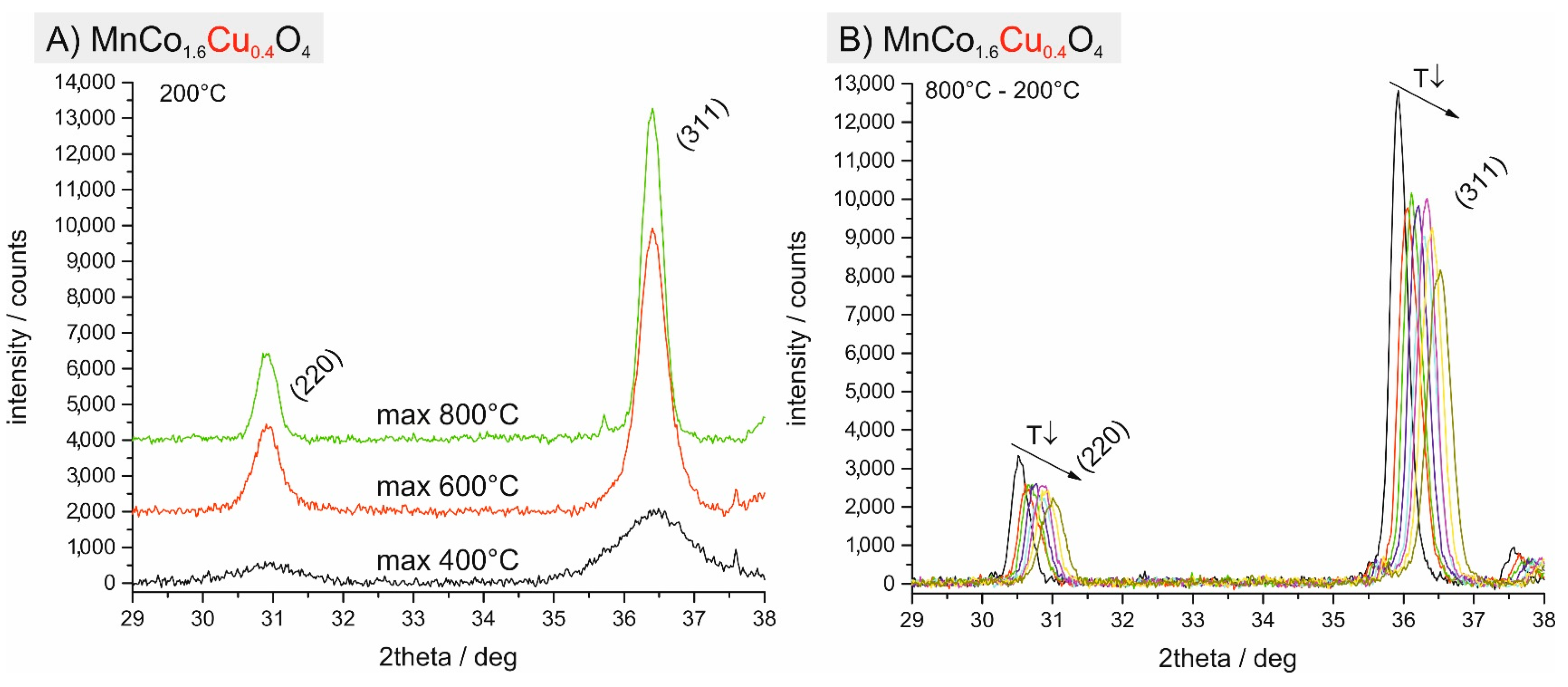
All four layers were investigated by in-situ high temperature XRD. As produced layers were evaluated first during heating to 400 °C, 600 °C and 800 °C in order to determine their crystallite size and growth using Equation (1). Additionally, after heating to 800 °C and holding for 1 h, XRD patterns were recorded every 100 °C during cooling to check the change in lattice parameters according to the Equation (2). Exemplary results obtained for the MnCo1.6Cu0.4O4 sample are shown in Figure 5 and summarized in Figure 6.
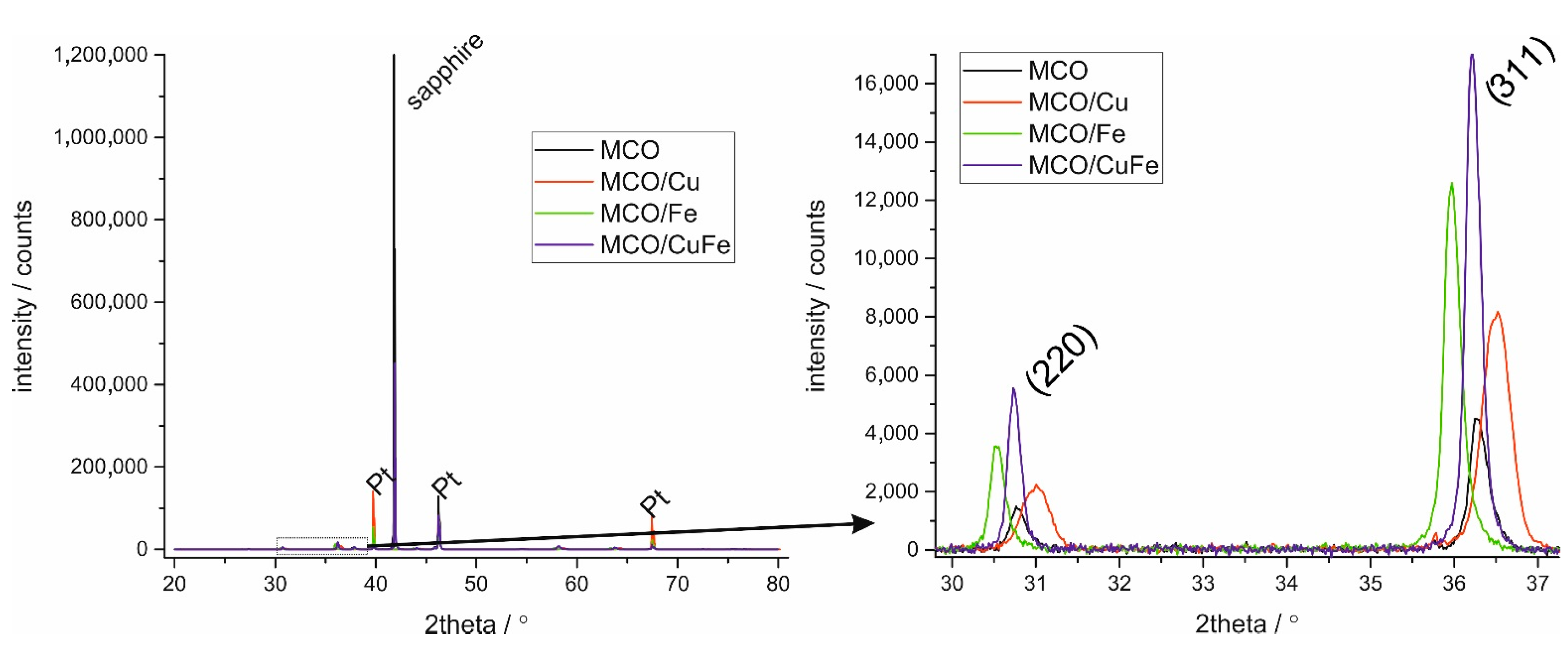
With an increase in maximum processing temperature, peaks become narrower and more intensive, as seen in Figure 5A and Figure 6A; this is related to growing crystallite size, as presented in Figure 5A and Figure 6A. For all samples, for the initial lowest processing temperature of 400 °C, peaks (220 and 311) are slightly shifted towards a higher 2θ range in comparison to layers processed at higher temperatures. This means that after the deposition at 390 °C, for very small crystallites (<10 nm), the lattice parameter is slightly smaller than after high temperature exposure. For layers processed at 600 °C and 800 °C, the lattice parameter stays the same, and only the crystallite size changes.
Crystallite growth evaluated by XRD peak broadening is similar for all layers. Crystallites grow from the initial ~6 nm to ~25 nm after processing at 800 °C. The Initial crystallite size is similar to the one observed previously by SEM in a similar system where MnCo2O4 precursors were impregnated into an MnCo2O4 matrix [11].
The variation in the lattice parameter (analyzing the structure as cubic) with temperature, measured during cooling from 800 °C is presented in Figure 6B. A clear effect of the introduced dopants on the lattice constant is observed. The addition of Cu lowers the lattice constant, whereas the addition of Fe increases the lattice constant. Simultaneous addition of the two dopants seems to cancel out the change in the lattice parameter. Observed changes are consistent with the ones reported in the literature [13,24,27].
XRD patterns measured at room temperature are presented in Figure 7. The different position of the 220 and 311 peaks represent a different cell size, as summarized in Figure 6B. Due to a low thickness of the film (~1 µm), the strongest peak comes from the sapphire substrate. After the heating to 800 °C, still only a single spinel phase is detected in the film.
In an MnCo2O4 spinel, the tetrahedral sites are occupied preferentially by Co2+ cations, with octahedral sites occupied by mixed valence Co2+, Co3+, Mn3+, Mn4+. As summarized by Masi et al. [13], the addition of Fe in place of Co results in substitution in the octahedral position of Co2+ by Fe3+, thus reducing the electrical conductivity. On the other hand, added Cu tends to occupy preferentially tetrahedral sites with the presence of Cu+/Cu2+ which additionally promotes oxidation of Mn3+ to Mn4+ to maintain charge neutrality. This, in turn, increases the number of different valence species, possibly leading to higher electrical conductivity and thermal expansion. In general, the spinel structure is quite complex, as cations (Mn, Co, Fe, Cu) can have different oxidation states and additionally some spinel inversion is possible, where “B” atoms can occupy “A” sites and lead to mixed composition of the cation sublattices. Therefore, no single defect model is proposed here.
High magnification surface SEM images are presented in Figure 8. The samples are shown after the high temperature XRD evaluation with a maximum temperature of 800 °C for two hours. Well sintered and dense films are observed for all samples. There are evident differences in grain sizes. The smallest grains are found for the undoped spinel (49 ± 12 nm), followed by MCO/Fe (67 ± 14 nm) and with the largest grains for the Cu containing layers: MCO/CuFe with 126 ± 12 nm and MCO/Cu with 178 ± 10 nm grains. Both dopants increase the average grain size, with Cu having a stronger effect. Enhanced sintering of the Cu containing spinels has been one of the reasons (in addition to enhanced electrical conductivity) for the focus on them [28,29]. Grain sizes determined by SEM are different from the grain sizes determined by the XRD. One possible explanation might be that due to a large strain from the deposition method and from the substrate TEC mismatch, the Scherrer formula becomes inaccurate due to peak modification in the XRD spectra by strain in the simple procedure used. Very good surface coverage of the sapphire substrates has been achieved by the spray pyrolysis method with dense coatings prepared at a maximum temperature of only 800 °C. Temperatures required to achieve dense layers prepared by spray pyrolysis are typically 200 °C–400 °C lower than temperatures in standard powder processing methods.
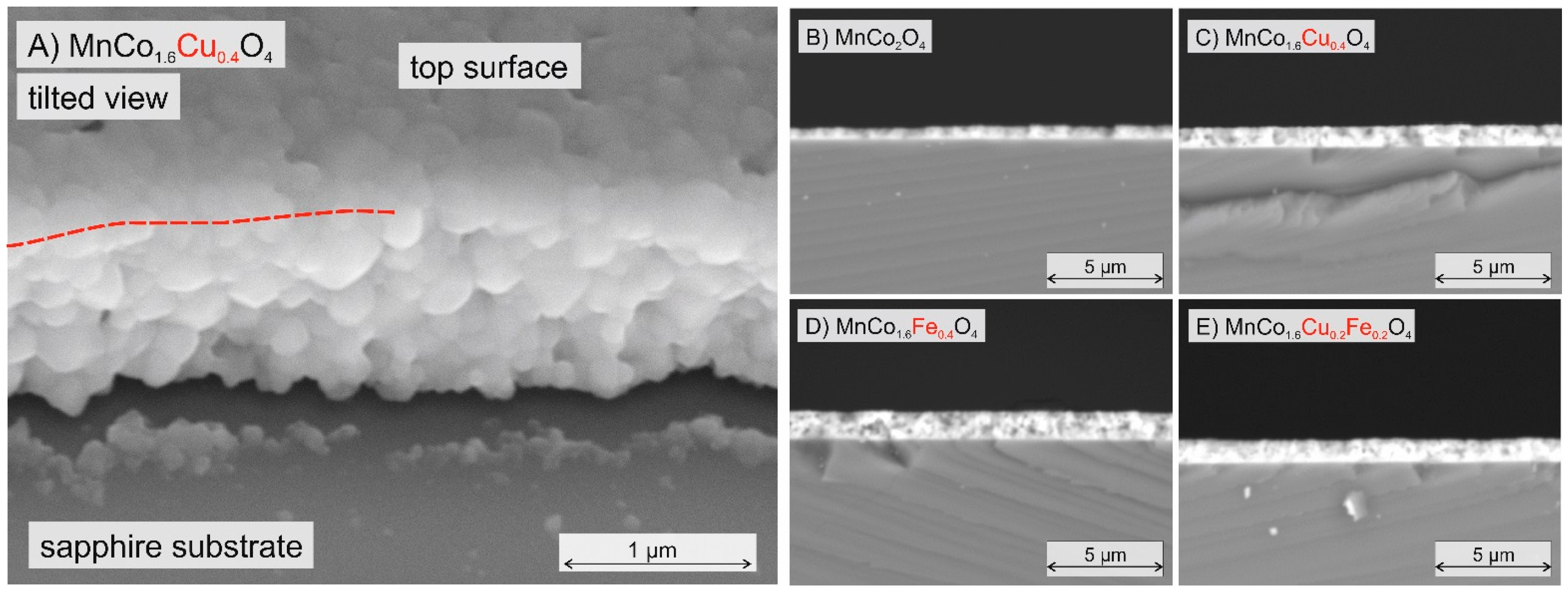
A tilted (37°) high-magnification image of a fracture cross section of the MnCo1.6Cu0.4O4 layer is shown in Figure 9A alongside lower magnification pictures of the fractured films. Thickness varies between ~0.7 µm for the MnCo2O4 to 1.2 µm for the MnCo1.6Cu0.2Fe0.2O4. The thickness of each coating is uniform over the whole cross section.
The thickness of the MnCo1.6Cu0.4O4 layer is built of approximately 10 grains. No large pores are observed in the cross section. Based on the surface and cross-section images, it seems that spray pyrolysis is a reliable and effective method for deposition of 1 µm thick layers of different compositions. In the previous deposition studies, it was not possible to obtain layers thicker than 0.3–0.5 µm in a single step process [30,31]. Increasing the molarity of the precursor solution allowed for obtaining thicker layers for the same deposition time, extending possible applications for the spray pyrolysis deposition method.
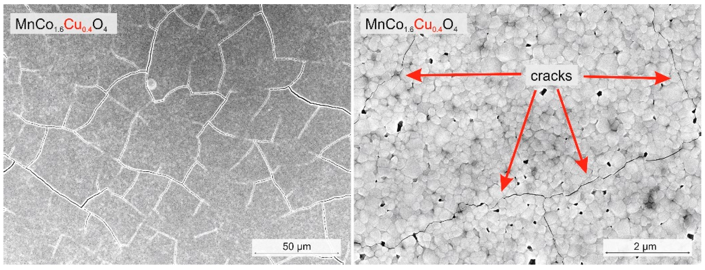
SEM pictures of the surface of the MCO/Cu layer are presented in Figure 10. Cracks are clearly visible over most of the sample surface. Both of the two MCO/Cu samples evaluated were cracked. In some places the layer spalled off; no cracks were observed for the other layers. These cracks were not detected in the as-produced sample; they must have formed during heat treatment of the layers. As previously described, irregularities in electrical conductivity measurements for the MCO/Cu layers were found. It is likely that the cracking of the layer is responsible for the step-changes in the measured electrical conductivity seen in Figure 3 and Figure 4.
Substitution of Co by Cu leads to an increase in the thermal expansion coefficient. According to Masi et al. [13] and Brylewski et al. [24], the thermal expansion coefficient (TEC between 30 °C–800 °C) of a partially Cu substituted spinel can reach ~15 ppm K−1. For partial Fe substitution a lowering of TEC is observed (to ~12.5 ppm K−1) and for the undoped spinel values between 12.5 and 14 are typically reported [13]. Sapphire substrate has a much lower TEC (~7.5 ppm K−1), so the stresses caused by the TEC mismatch are quite high. However, MCO/Cu and MCO/CuFe should have quite similar TEC. Other factors possibly influence the risk of cracking. The risk of crack formation further increases with film thickness, which varies somewhat between the samples. Cracking might also be influenced by grain growth and mass transport. Enhanced sintering of the Cu doped sample will cause lateral stress on the constrained layer and increase the risk of cracking. Simultaneous addition of Cu and Fe does not lead to such rapid grain growth and therefore doubly doped composition offers an important stability advantage.
4. Summary and Conclusions
High quality ~1 µm thick layers of MnCo2O4, MnCo1.6Cu0.4O, MnCo1.6Fe0.4O4 and MnCo1.6Cu0.2Fe0.2O4 have been prepared by spray pyrolysis at 390 °C. Electrical conductivity and microstructural changes of layers have been evaluated up to 800 °C. Spray pyrolysis is proven to produce dense spinel layers at temperatures of only 800 °C, which is lower than for standard ceramic processing methods. Maximum electronic conductivity is found for layers experiencing a maximum processing temperature of 700 °C, whereas no changes in the activation energy were noticed for different maximum processing temperatures. Electrical conductivity values obtained for the films agree well with the values reported for bulk samples. The addition of Cu increases the electrical conductivity and decreases the activation energy at high temperatures whereas the addition of Fe decreases the electrical conductivity. The addition of Cu increases the lattice parameter whereas the addition of Fe lowers the lattice parameter and for a Fe, Cu co-substituted spinel, lattice changes cancel out and resemble the undoped structure. Additionally, Cu visibly enhances grain growth and leads to cracked films. Simultaneous addition of Cu and Fe seems advantageous and offer the benefits of higher electrical conductivity and limited grain growth.
Acknowledgments
DTU Energy acknowledges support from the project 2015-1-12276 “Towards solid oxide electrolysis plants in 2020”, ForskEL, energienet.dk, while GUT acknowledges partly support from the project DZP/PL-TW2/6/2015 “Innovative Solid Oxide Electrolyzers for Storage of Renewable Energy”. Authors acknowledges for Statutory Funds for Research of GUT.
Author Contributions
Dagmara Szymczewska prepared the layers by spray pyrolysis and measured their electrical conductivity and wrote parts of the manuscript. S.M. analyzed the samples by SEM and XRD and wrote most of the manuscript. Peter Vang Hendriksen corrected the manuscript and discussed the research plan and the results. Piotr Jasinski corrected the manuscript and lead the discussions of the results.
Conflicts of Interest
The authors declare no conflict of interest.
References
- Ginley, T.; Wang, Y.; Law, S. Topological insulator film growth by molecular beam epitaxy: A review. Crystals 2016, 6, 154. [Google Scholar] [CrossRef]
- Deng, L.; Wang, K.; Zhao, C.X.; Yan, H.; Britten, J.F.; Xu, G. Phase and texture of solution-processed copper phthalocyanine thin films investigated by two-dimensional grazing incidence X-ray diffraction. Crystals 2011, 1, 112–119. [Google Scholar] [CrossRef]
- Lin, D.; Li, Z.; Li, F.; Cai, C.; Liu, W.; Zhang, S. Tetragonal-to-tetragonal phase transition in lead-free (kxna1−x) nbo3 (x = 0.11 and 0.17) crystals. Crystals 2014, 4, 113–122. [Google Scholar] [CrossRef]
- Chen, Y.; Santos, D.M.F.; Sequeira, C.A.C.; Lobo, R.F.M. Studies of modified hydrogen storage intermetallic compounds used as fuel cell anodes. Crystals 2012, 2, 22–33. [Google Scholar] [CrossRef]
- Molenda, J.; Kupecki, J.; Baron, R.; Blesznowski, M.; Brus, G.; Brylewski, T.; Bucko, M.; Chmielowiec, J.; Cwieka, K.; Gazda, M.; et al. Status report on high temperature fuel cells in Poland—Recent advances and achievements. Int. J. Hydrogen Energy 2017, 42, 4366–4403. [Google Scholar] [CrossRef]
- Wu, X.; Li, S.; Wang, B.; Liu, J.; Yu, M. Controllable synthesis of micro/nano-structured MnCo2O4 with multiporous core–shell architectures as high-performance anode materials for lithium-ion batteries. New J. Chem. 2015, 39, 8416–8423. [Google Scholar] [CrossRef]
- Jin, Y.; Wang, L.; Jiang, Q.; Du, X.; Ji, C.; He, X. Mesoporous MnCo2O4 microflower constructed by sheets for lithium ion batteries. Mater. Lett. 2016, 177, 85–88. [Google Scholar] [CrossRef]
- Akhtar, M.A.; Sharma, V.; Biswas, S.; Chandra, A. Tuning porous nanostructures of MnCo2O4 for application in supercapacitors and catalysis. RSC. Adv. 2016, 6, 96296–96305. [Google Scholar] [CrossRef]
- Larring, Y.; Norby, T. Spinel and perovskite functional layers between plansee metallic interconnect (Cr-5 wt % Fe-1 wt % Y2O3) and ceramic (La0.85Sr0.15)0.91MnO3 cathode materials for solid oxide fuel cells. J. Electrochem. Soc. 2000, 147, 3251–3256. [Google Scholar] [CrossRef]
- Talic, B.; Falk-Windisch, H.; Venkatachalam, V.; Hendriksen, P.V.; Wiik, K.; Lein, H.L. Effect of coating density on oxidation resistance and Cr vaporization from solid oxide fuel cell interconnects. J. Power Sources 2017, 354, 57–67. [Google Scholar] [CrossRef]
- Molin, S.; Jasinski, P.; Mikkelsen, L.; Zhang, W.; Chen, M.; Hendriksen, P.V. Low temperature processed MnCo2O4 and MnCo1.8Fe0.2O4 as effective protective coatings for solid oxide fuel cell interconnects at 750 °C. J. Power Sources 2016, 336, 408–418. [Google Scholar] [CrossRef]
- Montero, X.; Tietz, F.; Sebold, D.; Buchkremer, H.P.; Ringuede, A.; Cassir, M.; Laresgoiti, A.; Villarreal, I. MnCo1.9Fe0.1O4 spinel protection layer on commercial ferritic steels for interconnect applications in solid oxide fuel cells. J. Power Sources 2008, 184, 172–179. [Google Scholar] [CrossRef]
- Masi, A.; Bellusci, M.; McPhail, S.J.; Padella, F.; Reale, P.; Hon, J.E.; Wilckens, R.S.; Carlini, M. The effect of chemical composition on high temperature behaviour of Fe and Cu doped Mn-Co spinels. Ceram. Int. 2017, 43, 2829–2835. [Google Scholar] [CrossRef]
- Shaigan, N.; Qu, W.; Ivey, D.G.; Chen, W. A review of recent progress in coatings, surface modifications and alloy developments for solid oxide fuel cell ferritic stainless steel interconnects. J. Power Sources 2010, 195, 1529–1542. [Google Scholar] [CrossRef]
- Wang, K.; Liu, Y.; Fergus, J.W. Interactions between SOFC interconnect coating materials and chromia. J. Am. Ceram. Soc. 2011, 94, 4490–4495. [Google Scholar] [CrossRef]
- Jasinski, P. Electrical properties of nanocrystalline Sm-doped ceria ceramics. Solid State Ion. 2006, 177, 2509–2512. [Google Scholar] [CrossRef]
- Rupp, J.L.M.; Gauckler, L.J. Microstructures and electrical conductivity of nanocrystalline ceria-based thin films. Solid State Ion. 2006, 177, 2513–2518. [Google Scholar] [CrossRef]
- Rupp, J.L.M.; Infortuna, A.; Gauckler, L.J. Microstrain and self-limited grain growth in nanocrystalline ceria ceramics. Acta Mater. 2006, 54, 1721–1730. [Google Scholar] [CrossRef]
- Molin, S.; Jasinski, P.Z. Improved performance of LaNi0.6Fe0.4O3 solid oxide fuel cell cathode by application of a thin interface cathode functional layer. Mater. Lett. 2017, 189, 252–255. [Google Scholar] [CrossRef]
- Molin, S.; Chrzan, A.; Karczewski, J.; Szymczewska, D.; Jasinski, P. The role of thin functional layers in solid oxide fuel cells. Electrochim. Acta 2016, 204, 136–145. [Google Scholar] [CrossRef]
- Jasinski, P.; Molin, S.; Gazda, M.; Petrovsky, V.; Anderson, H.U. Applications of spin coating of polymer precursor and slurry suspensions for Solid Oxide Fuel Cell fabrication. J. Power Sources 2009, 194, 10–15. [Google Scholar] [CrossRef]
- Szymczewska, D.; Molin, S.; Chen, M.; Hendriksen, P.V.; Jasinski, P. Ceria based protective coatings for steel interconnects prepared by spray pyrolysis. Proc. Eng. 2014, 98, 93–100. [Google Scholar] [CrossRef]
- Brylewski, T.; Kucza, W.; Adamczyk, A.; Kruk, A.; Stygar, M.; Bobruk, M.; Dąbrowa, J. Microstructure and electrical properties of Mn1+xCo2−xO4 (0 ≤ x ≤ 1.5) spinels synthesized using EDTA-gel processes. Ceram. Int. 2014, 40, 13873–13882. [Google Scholar] [CrossRef]
- Brylewski, T.; Kruk, A.; Bobruk, M.; Adamczyk, A.; Partyka, J.; Rutkowski, P. Structure and electrical properties of Cu-doped Mn-Co-O spinel prepared via soft chemistry and its application in intermediate-temperature solid oxide fuel cell interconnects. J. Power Sources 2016, 333, 145–155. [Google Scholar] [CrossRef]
- Maier, J. Physical Chemistry of Ionic Materials: Ions and Electrons in Solids; Wiley: Stuttgart, Germany, 2004. [Google Scholar]
- Masi, A.; Bellusci, M.; McPhail, S.J.; Padella, F.; Reale, P.; Hong, J.; Robert, S.-W.; Carlini, M. Cu-Mn-Co oxides as protective materials in SOFC technology: The effect of chemical composition on mechanochemical synthesis, sintering behaviour, thermal expansion and electrical conductivity. J. Eur. Ceram. Soc. 2017, 37, 661–669. [Google Scholar] [CrossRef]
- Talic, B. Metallic Interconnects for Solid Oxide Fuel Cells: High Temperature Corrosion and Protective Spinel Coatings. Ph.D. Thesis, Norwegian University of Science and Technology, Trondheim, Norway, 2016. Available online: http://hdl.handle.net/11250/2404554 (accessed on 19 May 2017).
- Chen, G.; Xin, X.; Luo, T.; Liu, L.; Zhou, Y.; Yuan, C.; Lin, C.; Zhan, Z.; Wang, S. Mn1.4Co1.4Cu0.2O4 spinel protective coating on ferritic stainless steels for solid oxide fuel cell interconnect applications. J. Power Sources 2015, 278, 230–234. [Google Scholar] [CrossRef]
- Bobruk, M.; Durczak, K.; Dąbek, J.; Brylewski, T. Structure and electrical properties of Mn-Cu-O Spinels. J. Mater. Eng. Perform. 2017, 26, 1598–1604. [Google Scholar] [CrossRef]
- Szymczewska, D.; Chrzan, A.; Karczewski, J.; Molin, S.; Jasinski, P. Spray pyrolysis of doped-ceria barrier layers for solid oxide fuel cells. Surf. Coat. Technol. 2017, 313, 168–176. [Google Scholar] [CrossRef]
- Szymczewska, D.; Karczewski, J.; Chrzan, A.; Jasinski, P. CGO as a barrier layer between LSCF electrodes and YSZ electrolyte fabricated by spray pyrolysis for solid oxide fuel cells. Solid State Ion. 2017, 302, 113–117. [Google Scholar] [CrossRef]
Figure 1.
Schematic of the temperature profile (A) and sample holder for van der Pauw measurements (B).
Figure 1.
Schematic of the temperature profile (A) and sample holder for van der Pauw measurements (B).

Figure 2.
SEM surface image of the MCO/Fe layer (A,B) with EDS spectra of all prepared layers (C–F) for compositional analysis and XRD patterns (G) of prepared coatings (grazing incidence at 1.5 deg).
Figure 2.
SEM surface image of the MCO/Fe layer (A,B) with EDS spectra of all prepared layers (C–F) for compositional analysis and XRD patterns (G) of prepared coatings (grazing incidence at 1.5 deg).
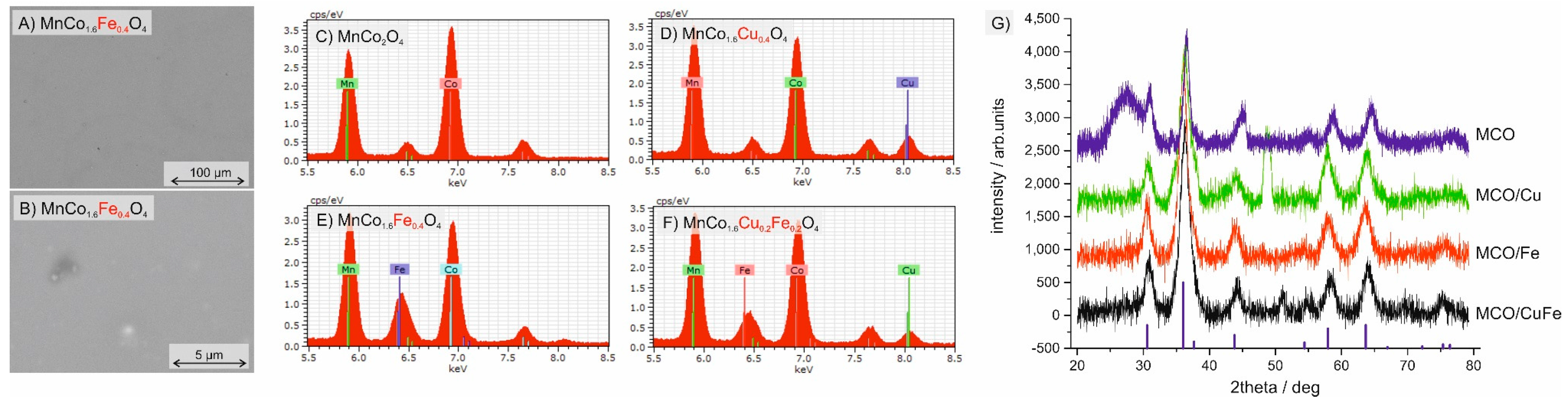
Figure 3.
(A–D) Electrical conductivity as a function of temperature plots for all samples after different heat treatments.
Figure 3.
(A–D) Electrical conductivity as a function of temperature plots for all samples after different heat treatments.
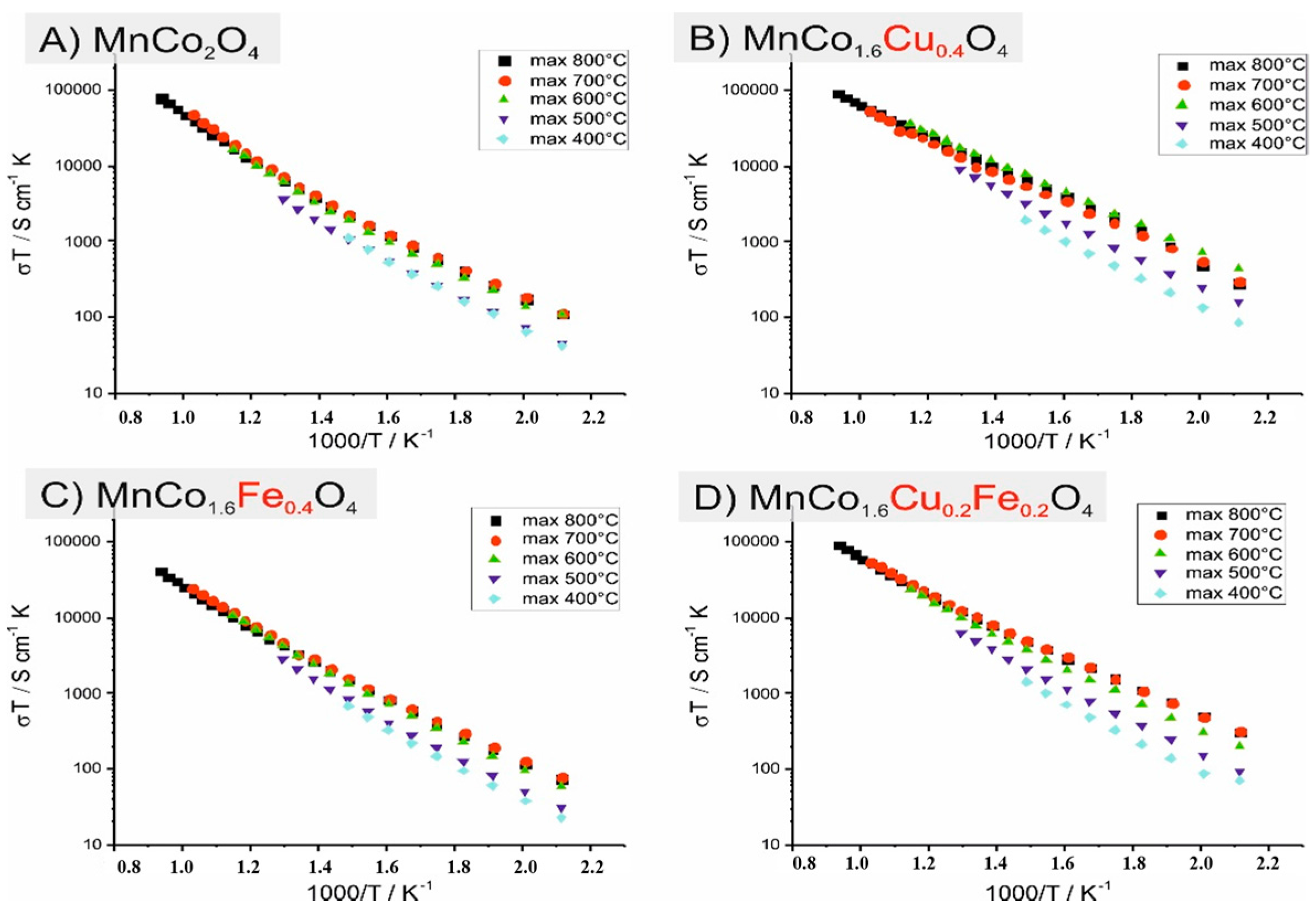
Figure 4.
Electrical conductivity of layers as a function of maximum exposure temperature: (A) 400 °C, (B) 500 °C and (C) 600 °C.
Figure 4.
Electrical conductivity of layers as a function of maximum exposure temperature: (A) 400 °C, (B) 500 °C and (C) 600 °C.
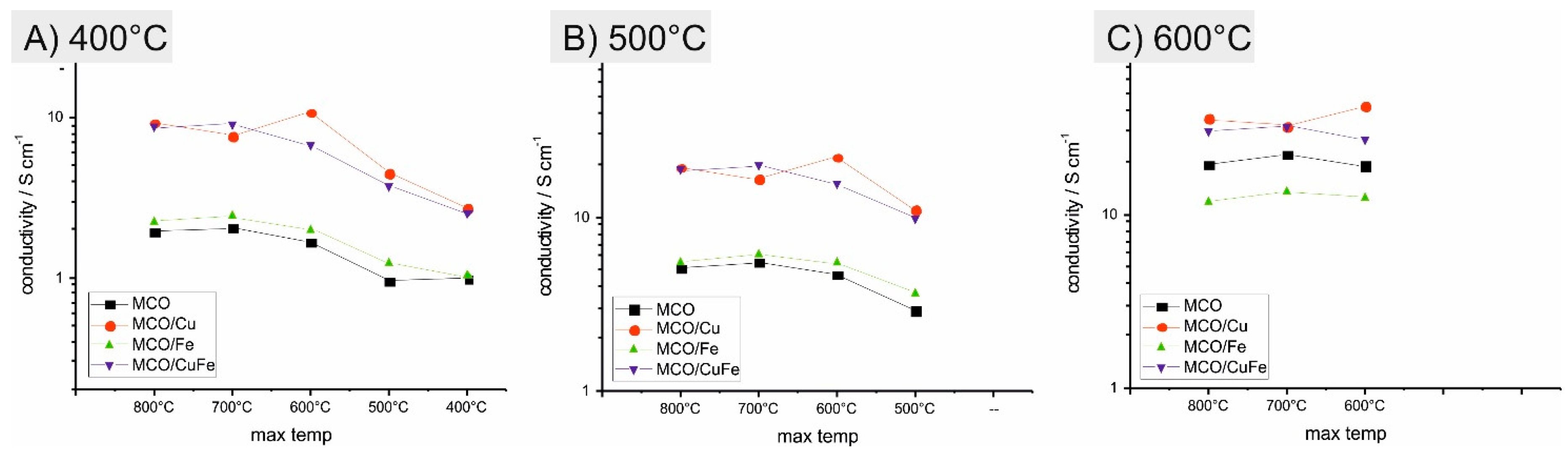
Figure 5.
High temperature XRD of the MCO/Cu layer: spectra at 200 °C of layers after different max exposure temperature (A) and cooling cycle from 800 °C to 200 °C (B).
Figure 5.
High temperature XRD of the MCO/Cu layer: spectra at 200 °C of layers after different max exposure temperature (A) and cooling cycle from 800 °C to 200 °C (B).

Figure 6.
Crystallite size of the spinel (A) and lattice change due to temperature (B).
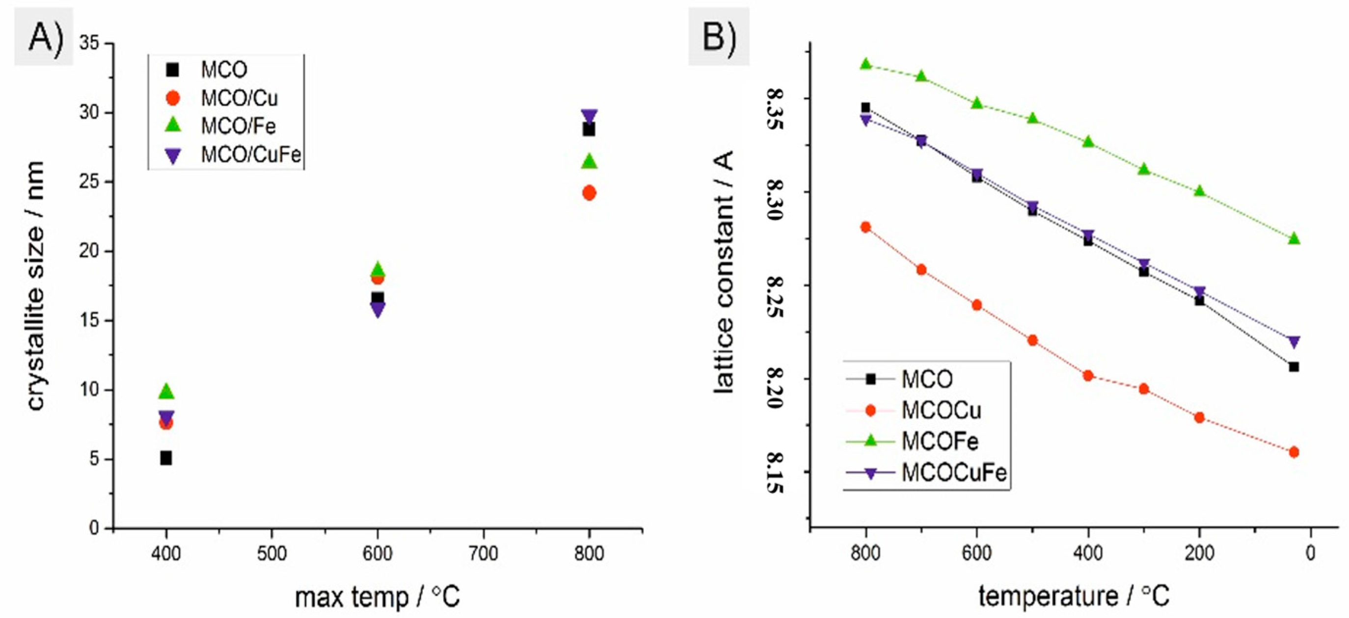
Figure 7.
XRD at RT after exposure to 800 °C.

Figure 8.
(A–D) SEM surface view of all layers after the electrical conductivity test.
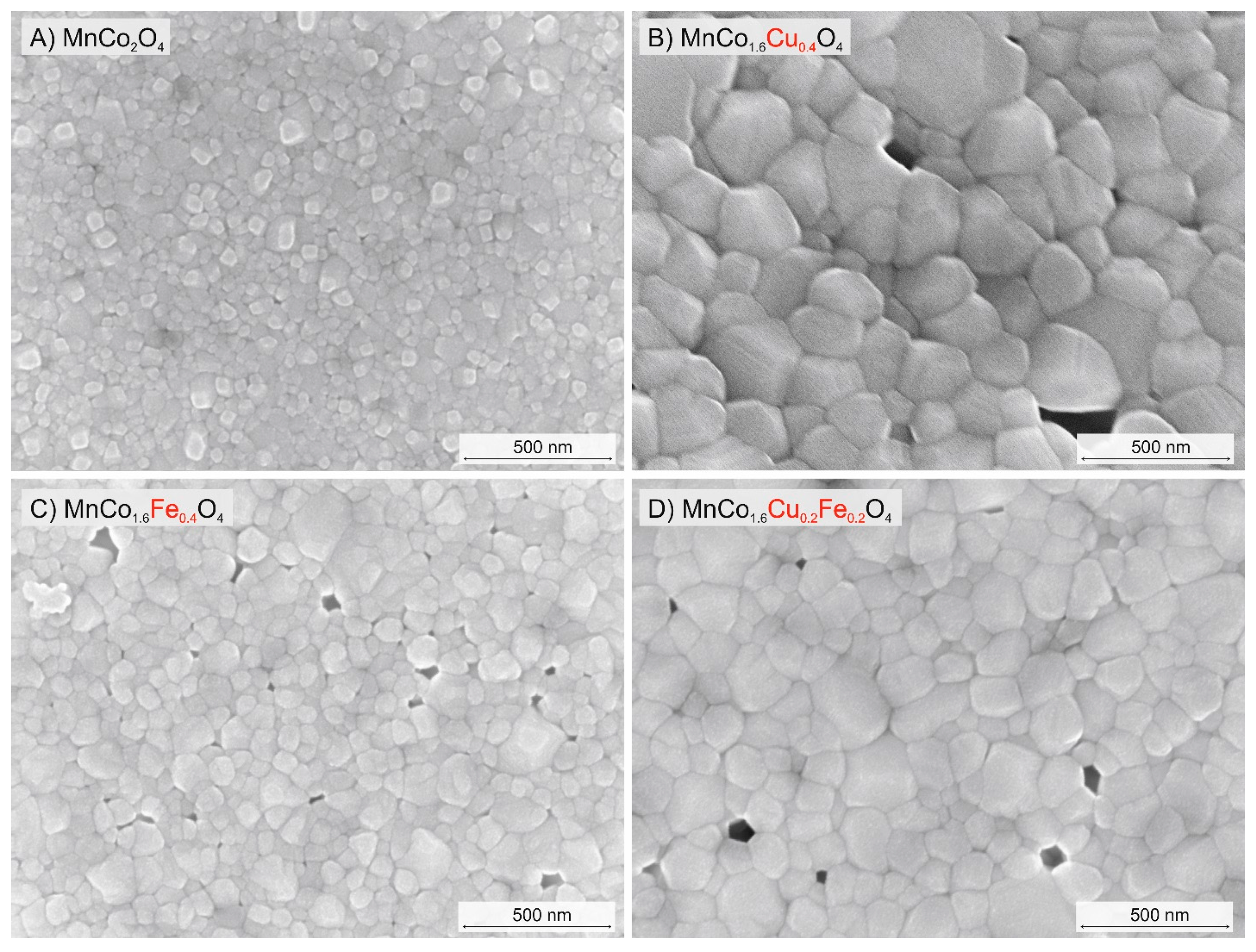
Figure 9.
(A–E) Fracture cross section SEM image of the MCO/Cu layer after the electrical conductivity test. Picture (A) taken at an angle of 37°.
Figure 9.
(A–E) Fracture cross section SEM image of the MCO/Cu layer after the electrical conductivity test. Picture (A) taken at an angle of 37°.

Figure 10.
SEM surface images showing cracks on the MCO/Cu layer after the electrical conductivity test.
Figure 10.
SEM surface images showing cracks on the MCO/Cu layer after the electrical conductivity test.

Table 1.
Chemical composition of coatings determined by energy dispersive spectroscopy (EDS) analysis.
Table 1.
Chemical composition of coatings determined by energy dispersive spectroscopy (EDS) analysis.
| MnCo2O4 | MnCo1.6Cu0.4O4 | MnCo1.6Fe0.4O4 | MnCo1.6Cu0.2Fe0.2O4 | |
|---|---|---|---|---|
| MCO | MCO/Cu | MCO/Fe | MCO/CuFe | |
| O | 60.0 | 56.7 | 60.2 | 58.5 |
| Mn | 12.3 | 13.4 | 12.7 | 12.6 |
| Co | 27.7 | 23.9 | 21.6 | 22.9 |
| Cu | 0 | 6.0 | 0 | 3.2 |
| Fe | 0 | 0 | 5.5 | 2.8 |
| (Co + Fe + Cu)/Mn | 2.25 | 2.23 | 2.14 | 2.30 |
| EDS determined stoichiometry | Mn0.92Co2.08 | Mn0.93Co1.66Cu0.42 | Mn0.96Co1.63Fe0.41 | Mn0.91Co1.66Cu0.23Fe0.20 |
Table 2.
Activation energy and electrical conductivity at 800°C for the coatings.
| σ 800 °C | EA (max 800 °C) | EA (max 700 °C) | EA (max 600 °C) | EA (max 500 °C) | EA (max 400 °C) | |||||
|---|---|---|---|---|---|---|---|---|---|---|
| Name/S cm−1/eV | HT | LT | HT | LT | HT | LT | HT | LT | ||
| MCO | 73.0 | 0.58 | 0.40 | 0.59 | 0.40 | 0.57 | 0.41 | 0.54 | 0.42 | 0.45 |
| MCO/Cu | 85.2 | 0.43 | 0.46 | 0.44 | 0.41 | 0.40 | 0.38 | 0.44 | 0.40 | 0.44 |
| MCO/Fe | 37.9 | 0.52 | 0.41 | 0.52 | 0.40 | 0.54 | 0.41 | 0.54 | 0.43 | 0.44 |
| MCO/CuFe | 86.6 | 0.48 | 0.38 | 0.48 | 0.38 | 0.47 | 0.40 | 0.48 | 0.41 | 0.44 |
© 2017 by the authors. Licensee MDPI, Basel, Switzerland. This article is an open access article distributed under the terms and conditions of the Creative Commons Attribution (CC BY) license (http://creativecommons.org/licenses/by/4.0/).
Share and Cite
MDPI and ACS Style
Szymczewska, D.; Molin, S.; Hendriksen, P.V.; Jasiński, P. Microstructure and Electrical Properties of Fe,Cu Substituted (Co,Mn)3O4 Thin Films. Crystals 2017, 7, 185. https://doi.org/10.3390/cryst7070185
AMA Style
Szymczewska D, Molin S, Hendriksen PV, Jasiński P. Microstructure and Electrical Properties of Fe,Cu Substituted (Co,Mn)3O4 Thin Films. Crystals. 2017; 7(7):185. https://doi.org/10.3390/cryst7070185
Chicago/Turabian StyleSzymczewska, Dagmara, Sebastian Molin, Peter Vang Hendriksen, and Piotr Jasiński. 2017. "Microstructure and Electrical Properties of Fe,Cu Substituted (Co,Mn)3O4 Thin Films" Crystals 7, no. 7: 185. https://doi.org/10.3390/cryst7070185
Note that from the first issue of 2016, this journal uses article numbers instead of page numbers. See further details here.