Article

Electro-Infiltration of Cytochrome C into a Porous Silicon Network, and Its Effect on Nucleation and Protein Crystallization—Studies of the Electrical Properties of Porous Silicon Layer-Protein Systems for Applications in Electron-Transfer Biomolecular Devices

by
Laura E. Serrano-De la Rosa
1,
Abel Moreno
2 and
Mauricio Pacio
1,*
1
Instituto de Ciencias-CIDS Benemérita Universidad Autónoma de Puebla, Ed. 130 C, Col. San Manuel C.P., 72570 Puebla, Mexico
2
Instituto de Química, Universidad Nacional Autónoma de México, Circuito Exterior C.U., 04510 Mexico City, Mexico
*
Author to whom correspondence should be addressed.
Crystals 2017, 7(7), 194; https://doi.org/10.3390/cryst7070194
Submission received: 6 May 2017 / Revised: 10 June 2017 / Accepted: 23 June 2017 / Published: 28 June 2017
(This article belongs to the Special Issue Protein Crystallization under the Presence of an Electric Field)

Abstract

:
In this work, we report the electrical properties of cytochrome C (Cyt C) inside porous silicon (PSi). We first used two techniques of protein infiltration: classic sitting drop and electrochemical migration methods. The electrochemically assisted cell, used for the infiltration by electro-migration, improved the Cyt C nucleation and the crystallization behavior due to the PSi. We were able to carry out the crystallization thanks to the previous infiltration of proteins inside the Si pores network. We then continued the protein crystal growth through a vapor diffusion set-up. Secondly, we applied both forward and reverse bias currents only to the infiltrated Cyt C. Finally, the electrical characteristics were compared to the control (the protein molecules of which were not infiltrated) and to the samples without protein infiltration. The linker used in the sitting drop method influenced the electrical properties, which showed a modification in the current density. The simple drop method showed a current density of ~42 A/cm2; when employing the electrochemical cell technique, the current density was ~318 A/cm2; for the crystallized structures, it was ~0.908 A/cm2.

Graphical Abstract

1. Introduction

Porous Si (PSi) is a versatile material that has generated interest because of its compatibility with biological materials and its different applications, such as in medicine [1,2] and molecular electronics [3,4,5]. Cytochrome C is a protein whose solid-state electrical properties have been studied in recent years [6,7,8]. Thin films of cytochrome C in its solid state have conduction mechanisms both inside the molecule and at the macroscopic level in the form of a thin film [9,10]. The possibility of using these conduction mechanisms, using PSi as a base for infiltrating cytochrome C, allows the study of the thin films’ electrical properties as a hybrid material—that is, an effective medium formed by PSi and cytochrome C.
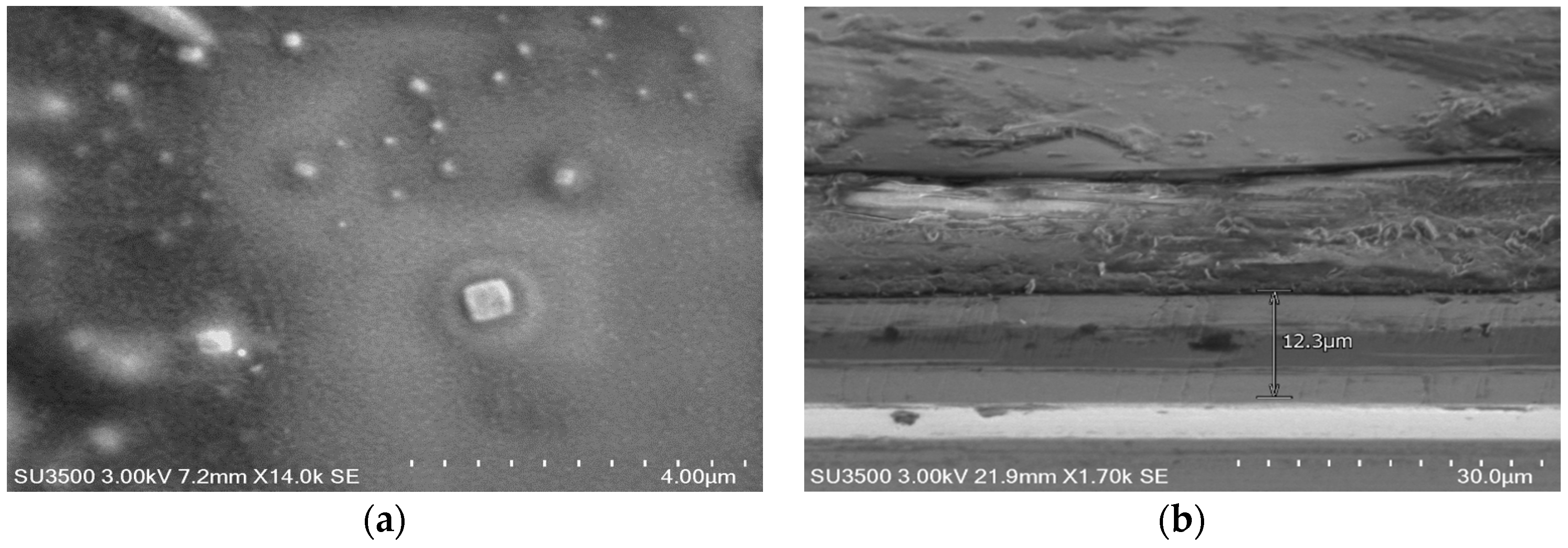
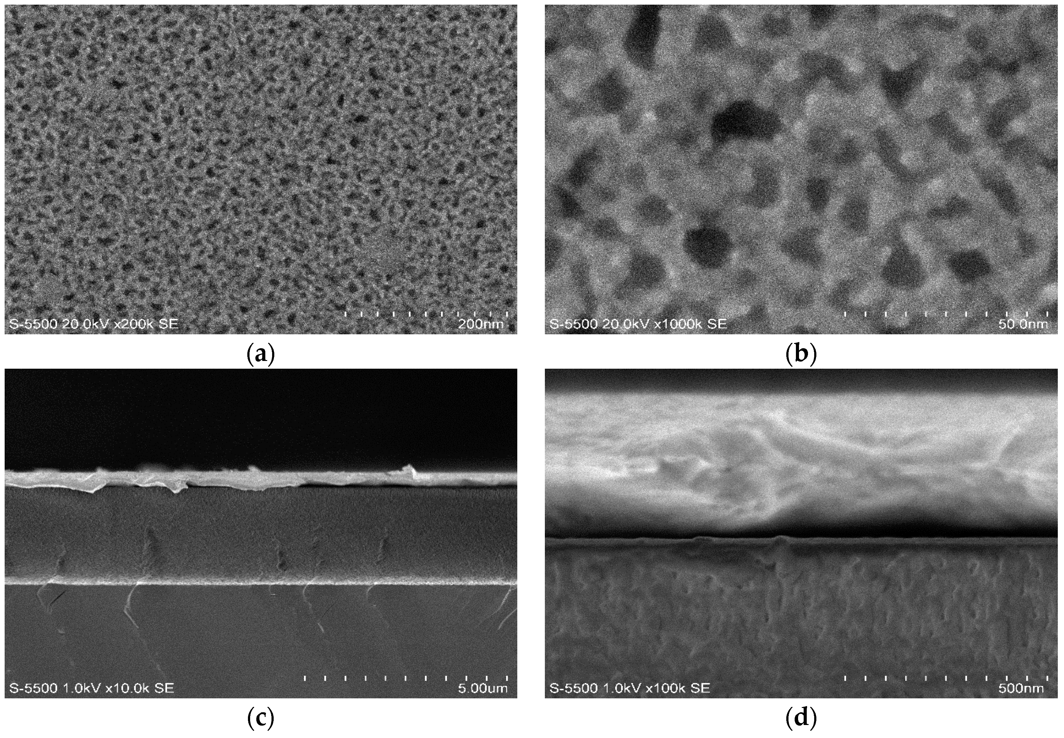
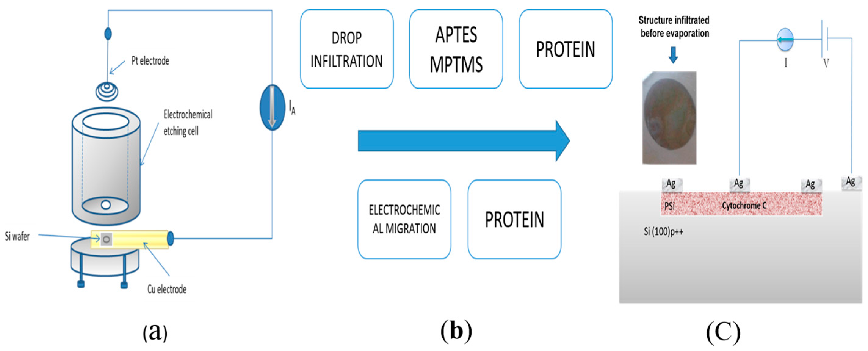
Different protein immobilization methods have been reported. The most common is the drop infiltration method or covalent bond immobilization [11,12], which consists of modifying the functional group of the PSi surface by thermal oxidation and subsequently with two silane groups. This method serves as a binder to immobilize the protein, thereby forming covalent bonds of the functional groups of the PSi surface with some of the functional groups of the protein. This method also allows its position to be identified with respect to the metallic contact or the substrate, thereby allowing electrical measurements to be carried out.
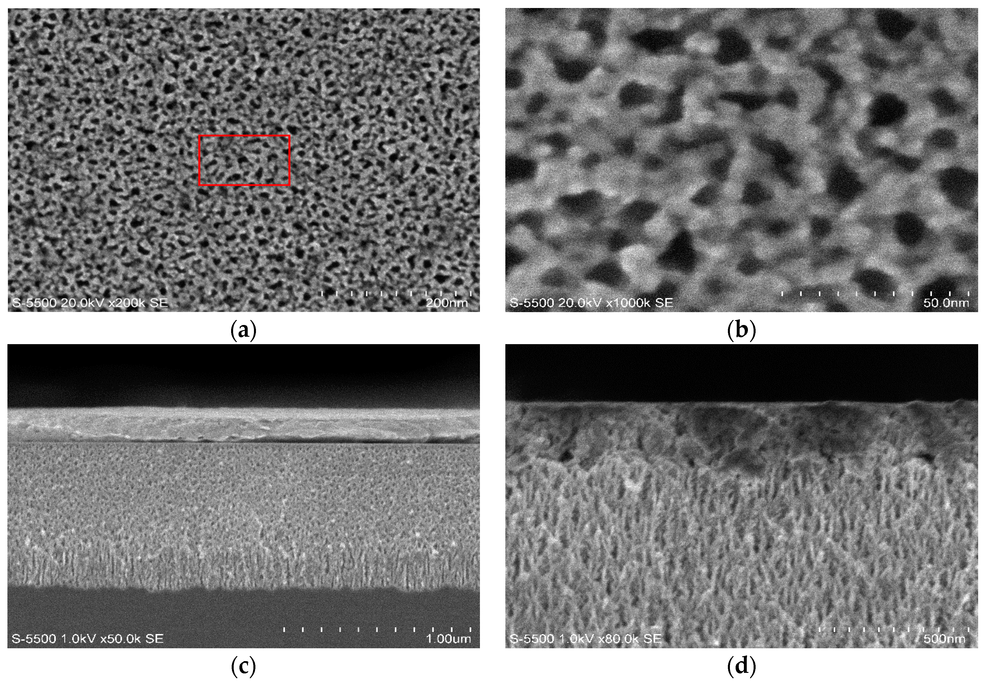
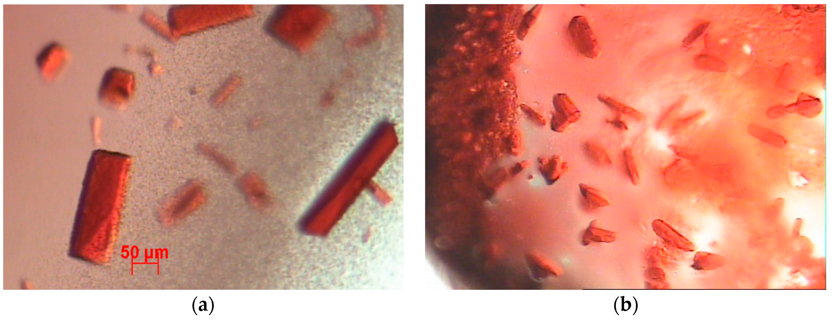
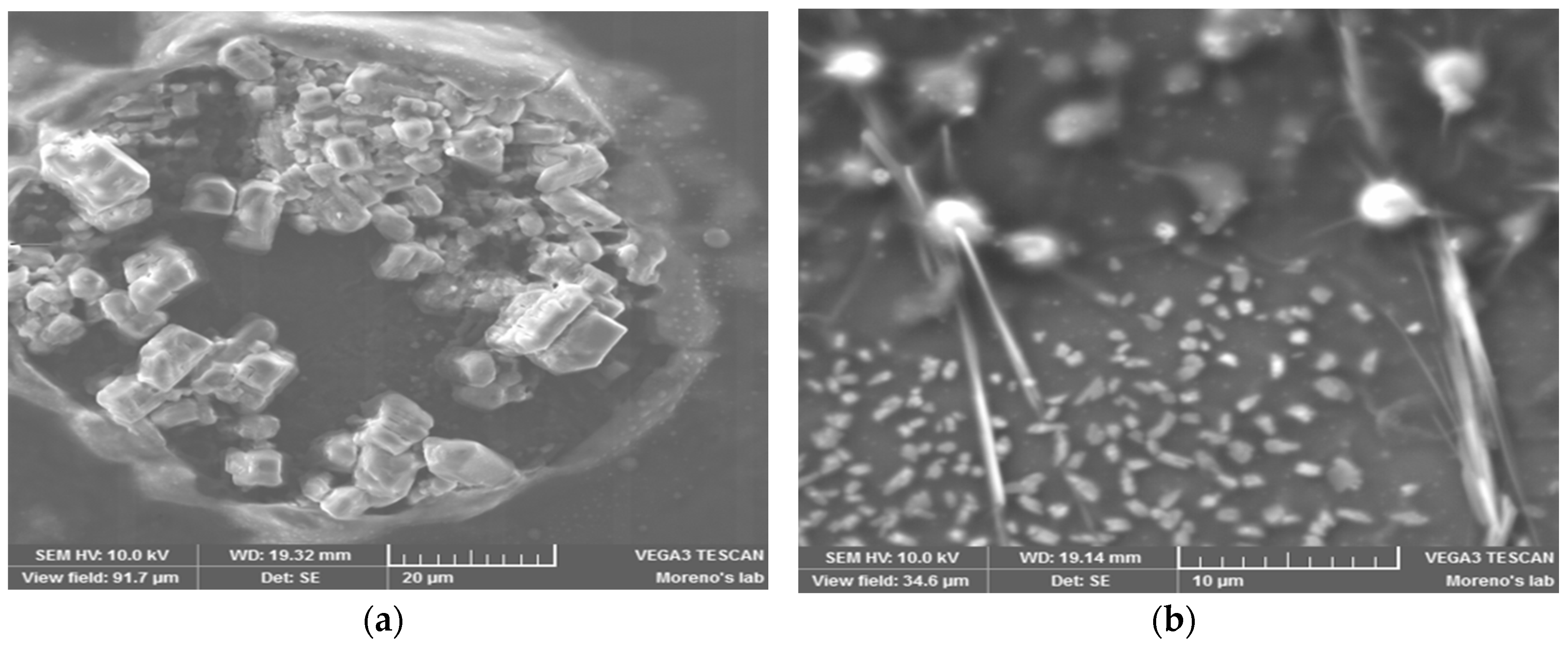
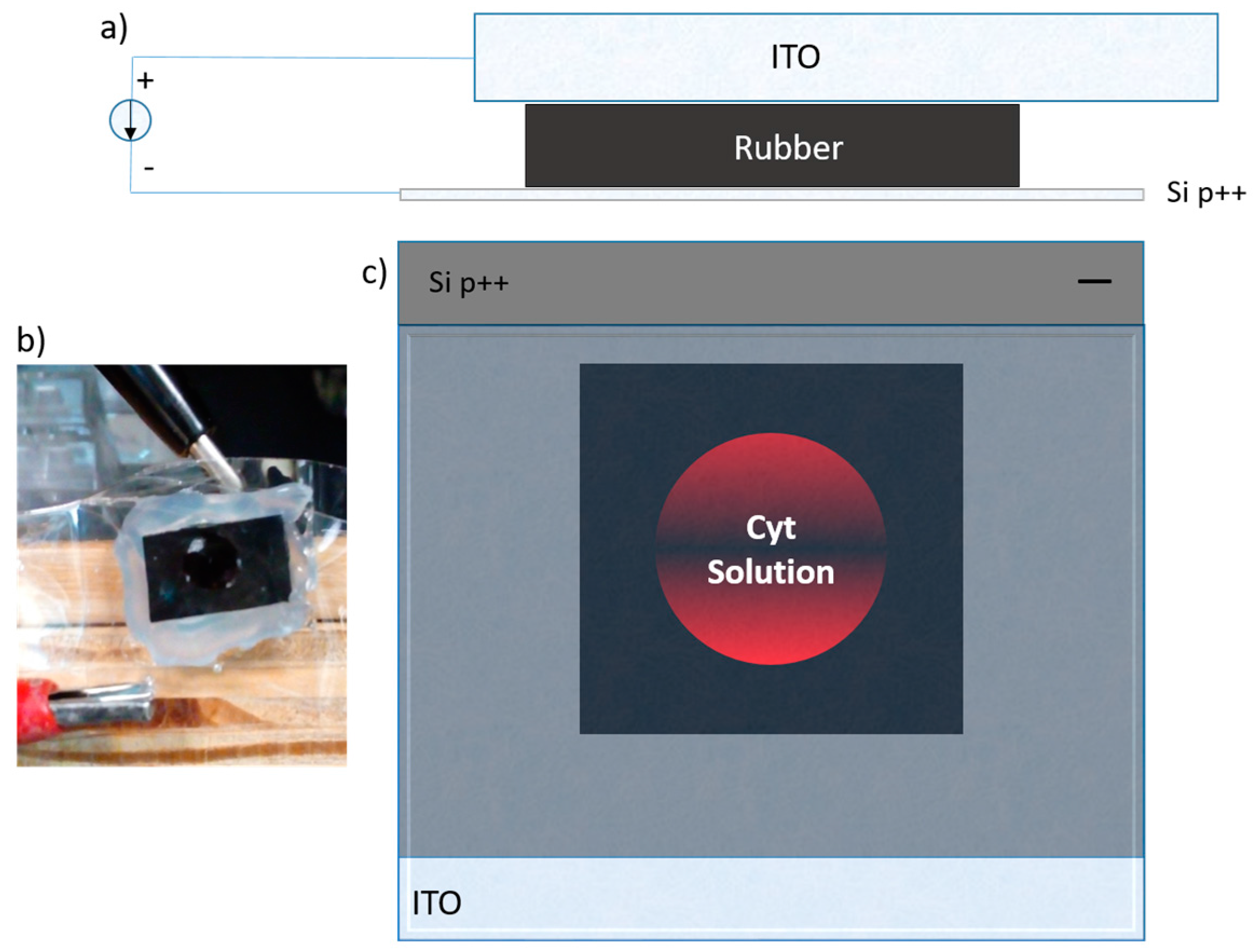
In this work, we used an ad hoc method for protein infiltration, based on preceding work [13] in which the protein crystallization was induced by employing magnetic and electric fields (DC) as nucleation-inductor factors. With this method, it is not necessary to do thermal oxidation or silane impregnation of the PSi; only an anodizing current is applied that causes the protein to infiltrate into the porous silicone due to the isoelectric point of the protein and the PSi. Subsequently, we continued with the protein crystal growth through a vapor diffusion set-up. We applied both forward and reverse bias currents only to the infiltrated Cyt C. Finally, the electrical characteristics were compared to the M/Ox/Si and M/PSi/Si structures, as well as to the control (where the protein molecules were not infiltrated) in the case of the crystallized samples.
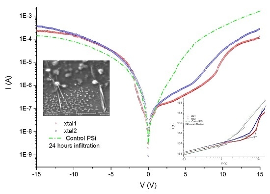
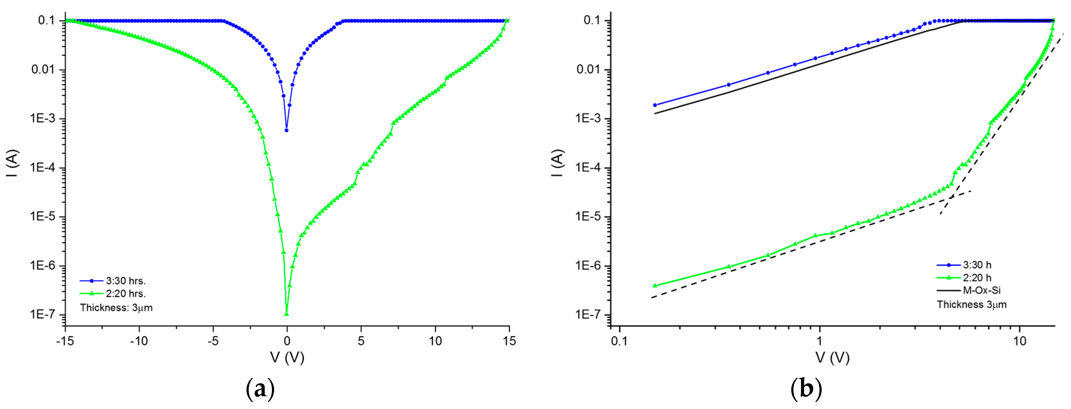
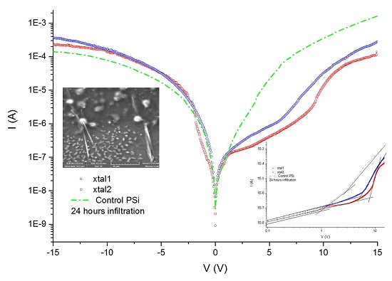
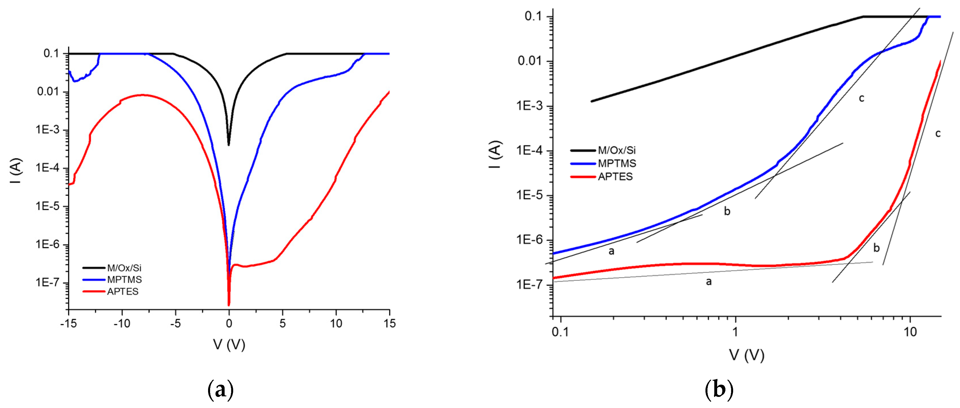
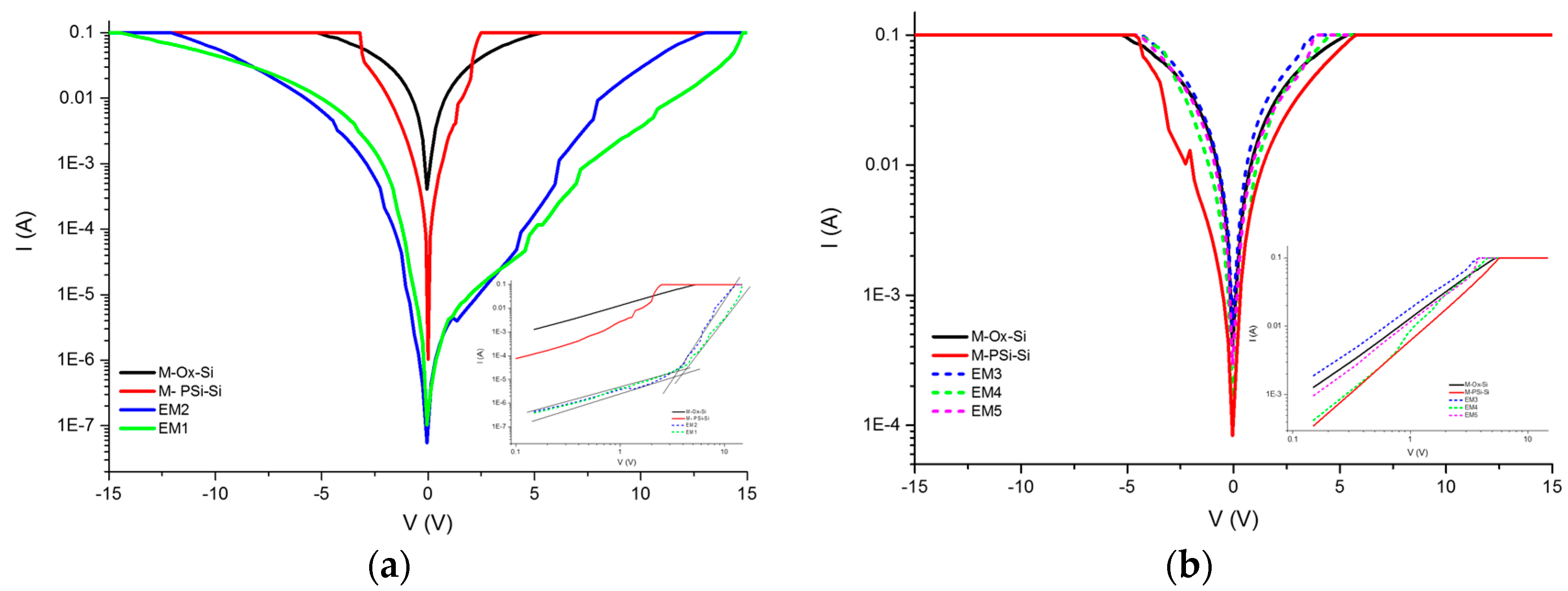
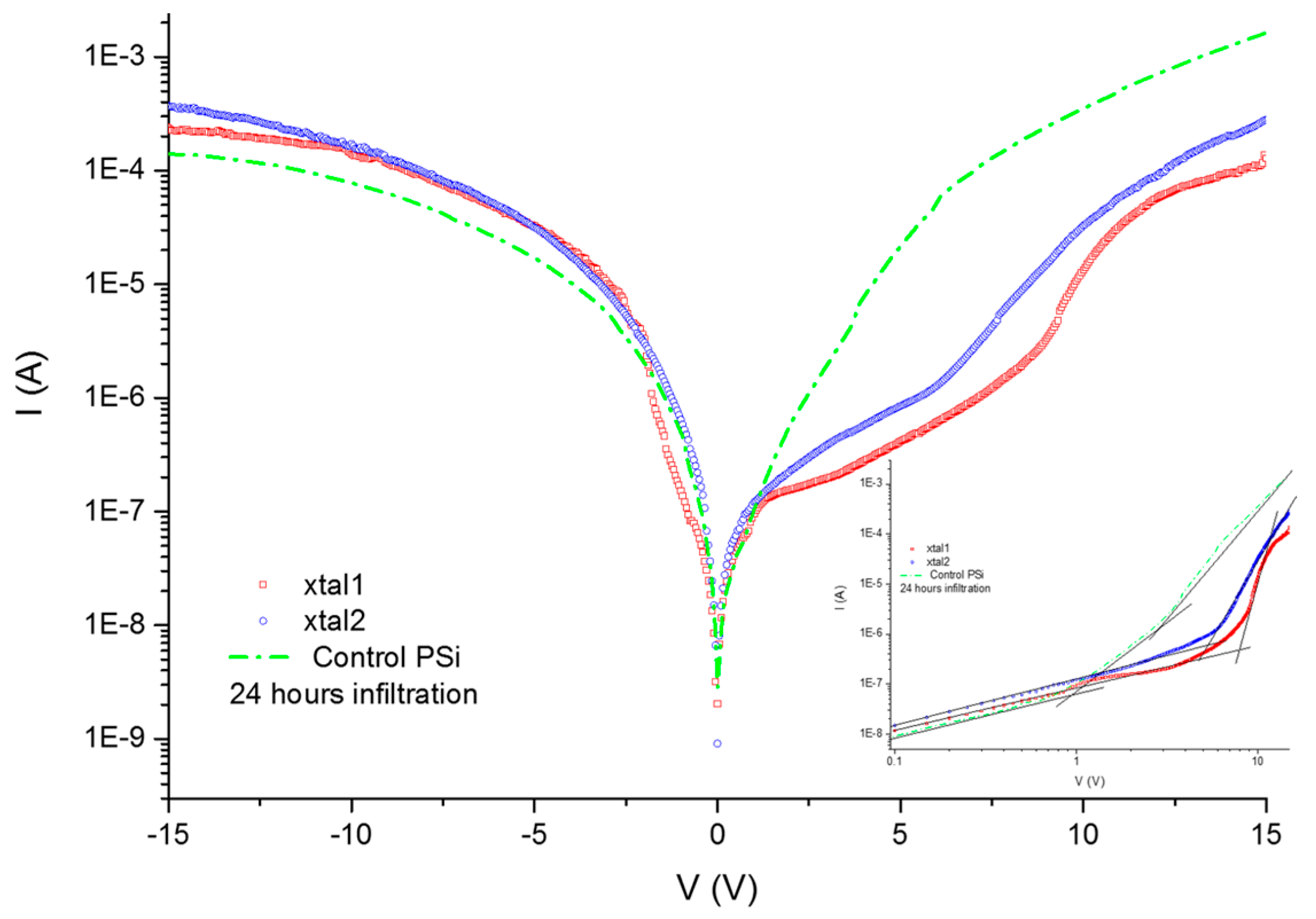
The electrical properties can be studied through the measurement of current–voltage (I–V) curves as a first approximation, to determine whether the material modifies its conductivity according to the method of infiltration. Once the protein is infiltrated by anodization, the I–V curves of the material are obtained. In comparison with the I–V curves of the immobilization, infiltration is larger by two orders of magnitude. The I–V curves of the crystallized proteins inside the PSi show a change in the order of magnitude and the current shows an asymmetric form. We then compared the level of current obtained for the crystallized protein with respect to the non-crystallized proteins. Our first approximation was based on the Schottky diode model, where the I–V curves let us determine the Schottky barrier height, considering the structure of the porous material as an effective medium.
R c = ( J V ) 1 ,   at   V = 0 .
The porous layer is considered as in the model proposed by Vikulov et al. [14], in the equation for current density. In order to determine the height of the barrier we assume the structure to be as in the Schottky diode and use the relation of specific contact resistance (Rc), the relation for a rectifying contact in our case, according to the experimental I–V curves. This allows us to obtain the relations for Rc [15]:
R c = ( kT e ) e x p ( e ϕ B kT ) A * T 2
where k is the Boltzmann constant, T is the temperature, A* is the Richardson constant and ϕB is the Schottky height barrier. Following the idea of the Schottky diode model, the ideality factor (n) can be calculated using the exponential relations:
J = A * T 2 exp ( q ϕ B kT ) [ e ( q V a nkT ) 1 ] ,
where n is the ideality factor, determined by evaluating the slope in the I–V curve’s exponential section.

2. Results and Discussion

2.1. SEM Images of the Porous Silicon Infiltrated Structures

2.1.1. Structures Infiltrated Using Silane-Coupling Agents

The PSi was stabilized by thermal oxidation at 1073.15 K, generating Si–O bonds. After this, the PSi/oxide layer was infiltrated employing silane-coupling agents, 3-aminopropyltriethoxysilane (APTES) and (3-Mercaptopropyl) trimethoxysilane (MPTMS), producing silane functional groups. The APTES [16] and MPTMS [17] molecule sizes are reported as 0.56 and 0.7 nm respectively. The silver (Ag) contact evaporated thickness is around 200 nm and the area covered by the circular Ag contact is 3.14 × 10⁻⁶ m2; this area is used to determinate the maximum current density J in the electrical characterization. Figure 1 shows SEM images of the structure M/PSi-APTES-Cyt C/Si. The image in Figure 1a presents the surface of the structure that was infiltrated; the pores observed are around 10 nm in diameter. The image in Figure 1b presents the center zone in (a) that is amplified to observe the pores clearly. The image in Figure 1c shows a cross view of the structure with the metallic contact evaporated on its surface. The top of Figure 1c shows the Ag contact interface; the bottom shows the Psi–Si interface. Through this scheme of the structure we carried out the electrical characterization. The thickness of the PSi layer is around 1 μm according the scale in Figure 1c. The image in Figure 1d shows the top of the structure without metal contact. Apparently, the infiltration process distorts the first 200 nm from the top to the PSi, and this shows the penetration distance inside the porous layer.
Similar images are shown for M/PSi-MPTMS-Cyt/Si in Figure 2. The image in Figure 2a corresponds to the structure after the Cyt C infiltration. The amplification in Figure 1b shows open pores, but in Figure 2b the pores appear closed; apparently, the MPTMS agglomerates on the surface. In Figure 2c, the structure cross view shows that the Psi layer thickness is ~4 μm. In Figure 2d, a difference in tone is shown at 100 nm from the top side of the layer, which suggests that the infiltrated materials are inside this first section of the layer.
In Figure 2d, the top of layer is darker than in Figure 1d and the top layer is thinner, at ~100 nm, suggesting that a layer of MPTMS was formed over the surface. That is in agreement with the dimensions of the silane molecules. On the other hand, the cross view in both of the structures reveals that the pores are empty in the structure with APTES, while the pores in the structure with MPTMS are filled or covered.

2.1.2. Structures Infiltrated by the Electrochemical Migration Method

In the second infiltration method, the PSi was stabilized as described in the previous subsection, without infiltration with silane-coupling agents. The electrochemical migration method was used to infiltrate the Cyt C into the walls of the PSi. Figure 3 shows SEM images of 12 μm and 3.3 h of infiltration of the sample. In Figure 3a, the top view of the sample, pores cannot be observed as they are completely filled or covered by protein. Figure 3b shows the thickness of the PSi layer. On the top, a thicker protein layer is present, around the same thickness as the PSi layer; this explain why no pores are observed in Figure 3a.

2.1.3. Structures Infiltrated with Crystallized Cytochrome C

In order to know the difference between the infiltration processes used in this work, we used a control sample, prepared using the hanging-drop vapor diffusion method (see Section 3.4), which does not present electrochemical migration in the crystallization process of Cyt C. In Figure 4, SEM images for both cases are shown. In Figure 4a, the surface of the control sample, the crystals formed have a size of ~10 μm. It should be noted that the protein in this work is not purified, so the form and size of the crystals obtained were smaller and differently shaped compared to the orthorhombic crystals reported by Mirkin et al. [18]. The image in Figure 4b corresponds to the electrochemical migration sample; in this case, the crystals are on the sample surface. They have a size of ~1 μm, and the orthorhombic shape is not well-defined. The needles in the image correspond to the surfactant residues.
The results obtained from the SEM images can be compared with optical images of crystallized Cyt C, both purified and non-purified, infiltrated into PSi. Figure 5a shows that the size and orthorhombic shape of the crystals is larger and well-defined, respectively, for the purified Cyt C; the shape corresponds to the isoform F1, in agreement with that reported for this protein elsewhere [19]. In Figure 5b, which corresponds to the unpurified Cyt C infiltrated in the PSi, the crystals are smaller, irregular and less well-defined than those for the orthorhombic-shaped crystals. The same behavior is observed in the SEM images (Figure 4).
The crystallization of cytochrome C was possible even with the unpurified protein; the effect of the electromagnetic field on the growth of protein crystals has already been reported [18]; however, the possibility of obtaining protein crystals with unpurified proteins opens the possibility of other applications that are more economical and simple in terms of crystallization time.

2.2. Electrical Characterization

The electrical characterization is based on I–V curve measurements. The semi-log I–V curves were measured at room temperature. To understand the conduction mechanism for the samples obtained, the log–log I–V curves for the APTES sample are shown. In the equipment used to measure the I–V curves, a compliance voltage limits the intensity of the current, so the curves show a flat region when the current reaches 0.1 A. At that point, the current density J was determined using the contact area value.

2.2.1. I–V Measurements of APTES and MPTMS Structures

Figure 6 shows the I–V curves for the M/PSi-APTES-Cyt C/Si and M/PSi-MPTMS-Cyt C/Si structures. The black line is the measurement of the M/Ox/Si structure. The graphic in Figure 6b shows the log–log I–V of the forward bias. The current from MPTMS is higher and more symmetric than that from APTES. The behavior of the MPTMS structure is closer to the M/Ox/Si.
The log–log I–V curves are clearly different for both structures. The graphic in Figure 6b considers the infiltrated PSi an effective medium, which enables us to consider three sections in the curve, related to different conduction mechanisms. Figure 6b shows the following behavior: Section (a) is associated with the deep traps at the interface of the M/PSi-silane coupling agent–Cyt C, and the dependence is linear, modifying the slope in the low-voltage region. In Section (b), the current increases exponentially, the slope is the ideality factor in the Schottky structures. In this section, the dominant conduction mechanism is recombination-tunneling [20]. In Section (c), the current follows the potential relation >>2, which indicates that the transport mechanism is dependent on temperature; this requires measurements at different temperatures [21]. Table 1 shows the slopes determined from the I–V curves for each section in Figure 6b.

2.2.2. I–V Measurements of Structures Obtained by the Electrochemical Migration Method

For infiltration by electrochemical migration, M/PSi-Cyt C/Si structures were fabricated. The infiltration times were 2.2, 3.3 and 24 h. The thicknesses are listed in Table 2. Figure 7 shows the log I vs. V curves for different times and thicknesses; curves for M/Ox/Si and M/PSi/Si structures are in both graphics for comparison. Figure 7a, the graphic for 2.2 h, shows the current intensity for layers with 10 and 3 µm thickness; the current is lower than the PSi and the shape is not symmetrical. The inset is the log–log I–V curves; two slopes are identified and the values are similar for both samples; this indicates that the electrical behavior is independent of the thickness of the PSi layer. The values for the slopes are listed in Table 3.
The slope in Section (a) for the two samples is between 1 and 2, thus the predominant conduction mechanism is recombination-tunneling. The graphic in Figure 7b shows the current intensity for samples infiltrated for 3.3 h. The slope values confirm behavior close to that of the M/Ox/Si structures, and in the case of the EM3 sample the current is above the conductive behavior of those structures. In Table 4, the slope values are listed, including the values for the M/Ox/Si and M/PSi/Si structures. As in the case of 2.2 h samples, the behavior is independent of the thickness of the PSi layer.
The graphic in Figure 8a shows the I–V curves for the 2:20 and 3.3 h samples with 3 μm; the structure infiltrated for 3.3 h has a current higher than that of the M/Ox/Si structure. Infiltration time is a factor of the quantity of Cyt C infiltrated into the PSi for the M/PSi-Cyt C/Si structure. This agrees with the SEM image in Figure 3. In Figure 8b, the log–log I–V curves for the forward bias, obtained from the graphic in Figure 8a, allow us to compare the magnitude order of current I and to gain knowledge of the conduction mechanisms.

2.2.3. I–V Measurements of Structures after the Crystallization Process

In Figure 9, I–V curves for M/PSi-Cyt C/Si structures after the crystallization process, are shown. The infiltration time was 24 h. The black line corresponds to the control sample (M/PSi-Ox/Si structure) without Cyt C infiltration. The crystallization process reduces the current intensity and, at the same time, changes the conduction mechanisms. This behavior is close to that observed in Figure 6a. The inset graphic shows the log–log I–V curves; as in the structures in Figure 7a, only the deep trap and recombination-tunneling conduction mechanisms can be observed. The slopes from these structures are listed in Table 5.

2.3. Determination of Electrical Parameters

As already mentioned, the structures in this work were considered to be like a Schottky diode. The electrical parameters were determined by Equations (1)–(3). The contact resistance (Rc) values were obtained from the I–V curves; as indicated in Equation (1), this is the inverse of derivate respect to applied voltage, evaluated in V = 0. The values of Rc were used in Equation (2) in order to obtain the height barrier (ϕB); thus, from Equation (2), the relation for the height barrier is as follows:
ϕ B = kT e l n ( eA * T 2 R c kT )
Table 6 lists the electrical parameters obtained from the I–V curves; that is, Rc, ϕB and the maximum current density J. The value of J, as we mentioned in Section 2.3, was obtained at the point that the compliance voltage limits the measuring instrument, causing the current to become a flat line; in the case of the crystallized samples, the current was below the limit mentioned, so the value of J was determined at the maximum value of V = 15 volts.
The ϕB values listed in Table 6 do not seem to be consistent with the current density, which provides an idea about the equations used in this work; since this is a first approximation we consider that the model must be improved, considering the conduction mechanisms of both the PSi and Cyt C separately.

3. Materials and Methods

3.1. APTES and MPTMS Structures

Figure 10 shows a scheme of the process for the obtainment of the structures. In the first part, the PSi layers were obtained by electrochemical anodization. Next, these layers were placed in a furnace for the oxidation process, followed by the infiltration processes through the simple drop and electrochemical migration methods. Finally, all samples were evaporated on a metallic contact; in this case, with Ag circles. The electrical characterization was realized for all samples; the I–V measurements were taken in the transversal mode as shown in Figure 10c as published elsewhere [21].

3.1.1. PSi Preparation

The PSi layers used in this work were obtained by the electrochemical etching of p-type Si, phosphorus-doped, single-side-polished and 100-oriented silicon. Highly doped substrates (p++) with a resistivity of <0.005 Ω·cm were used. The electrolyte consisted of a mixture of aqueous 40 wt % HF (hydrofluoric acid) and absolute ethanol (99.9%) in a volumetric ratio of 1:1. An etching process was performed using a small cell made of Teflon, as described in Figure 10a. The etching process was executed to obtain layers with 60% porosity, determined by the gravimetric method [22]. The gravimetric method and profiler measurements were used to determine the growth velocity and thickness of the layers

3.1.2. Oxidation and Silane Stabilization

Before the infiltration process, the PSi must be modified due to the functional groups on the surface. The oxidation and silane stabilization processes allow the immobilization of proteins on the surface of the PSi. The thermic oxidation of PSi consists of placing the samples inside a tubular furnace (25–1200 °C) with a controller 1/16-DIN PROFILER/CONTROLLER. The process was carried out with an oxygen atmosphere: firstly, pre-oxidation at 300 °C for 10 min, followed by a temperature ramp of 100 °C/min up to 800 °C. This temperature was maintained for 3 min, at which point the furnace was turned off. The samples were removed to room temperature and stored in a desiccator.
The two silane stabilization processes (employing silane-coupling agents APTES and MPTMS) were performed: (1) the samples were dipped in 3-aminopropyltriethoxysilane (5% in toluene) for 1.5 h, then dipped in toluene and then dried with N2 flow and stored at room temperature; (2) the samples were immersed in 3-mercaptopropyltrimethoxysilane (5% in isopropanol) as the functional reagent for 2 h. Samples were then removed and washed with isopropanol, then dried with N2 flow and stored at room temperature until use.

3.1.3. Drop Infiltration

Once the samples were stabilized by the silane-coupling agents, a drop of Cyt C solution was deposited on the surface of the porous layer for 24 h at 277 K. After that, the remaining solution was retired and the samples were covered for 12 h at room temperature. The solution was prepared with a concentration of 5 mg/mL of cytochrome C from Sigma–Aldrich and a phosphate buffer solution of pH 7.0 and 1 M from J. T. Baker.

3.2. Electrochemical Migration Method

The electrochemical migration process consisted of a crystal growth cell connected to a DC power supply, which allows the protein to migrate inside the PSi without the silane stabilization process. The DC apparatus was a Potentiostat/Galvanostat (Vimar, Mexico) which supplied a direct current of 2 μA for 2.2, 3.3 and 24 h. The construction of the electrochemical migration cell was made following the procedure of Pareja-Rivera et al. [13], using the Si wafer as a cathode. The description of this cell is given in Appendix A.

3.3. Sample Preparation for I–V Measuurements

For the I–V measurements, all samples were evaporated on a metallic contact, using a stainless steel mask with circles of 2 mm diameter. Silver wire from Sigma–Aldrich with 99.99% purity was used at 1 × 10⁻⁶ torr. Other authors report an additional step after evaporation: their samples were subjected to heat treatment at 300 °C in order to ensure the ohmic contact. In this work, because of the protein characteristics, this heating was not possible. A Keithley 4200 A Semiconductor measuring system, using tungsten micrometric positioning tips, was used to obtain the I–V curves [21].

3.4. Crystallization Process

The crystallization of the cytochrome C used for the control sample was prepared by using the hanging-drop vapor diffusion method on EasyXtal crystal support plates (QIAGEN Lot No. 55402874). The crystallization conditions were those published by Sanishvili et al. [23], who also crystallized the oxidized form of native Cyt C. The reservoir (750 μL) contained 30% PEG-1000 in 50 mM sodium phosphate pH 7.0. Droplets of 4 μL (2 μL protein + 2 μL precipitant) containing 25 mg/mL of cytochrome C with 25% PEG-1000 both in the same buffer phosphate pH 7.0 were incubated at 277 K for 32 days. Under the conditions used by Sanishvili et al., we obtained poorly shaped aggregates. In our previous publication [18] using re-purified Cyt C, these aggregates were used as microseeds and were transferred (by means of a cat whisker) to pre-equilibrated droplets containing 22 mg/mL of protein and 25% PEG-1000 both prepared in 50 mM buffer phosphate pH 7.0. After one week, several orthorhombic crystals could be obtained
Cytochrome C was infiltrated as described in Section 3.2. It improved the Cyt C nucleation and the crystallization behavior due to the PSi. Though the microcrystals deposited on silicon were analyzed by scanning electron microscopy using a STEM Vega 3 from TESCAN (Czech Republic), they faced the risk of being destroyed when collecting images. The imaging was performed using low pressure to avoid damaging the samples.

4. Conclusions

The PSi layer was obtained by the electrochemical etching of p-type Si with 60% porosity determined by the gravimetric method. This layer was oxidized by thermal oxidation to generate Si–O bonds. These bonds were employed to pin up the silane groups obtained by the infiltration of the silane-coupling agents APTES and MPTMS. The silane groups allow the interaction with the protein and the different structures used in this work. We used two protein infiltration techniques: the sitting drop technique and electrochemical migration method. Cyt C was infiltrated into the PSi by using purified and non-purified forms. With the M/Psi-silane-coupling agent-Cyt C/Si and M/PSi-Cyt C/Si structures were obtained. The crystallization of proteins was found to be feasible on the surface of PSi. I–V curve measurements were made of these structures, which determined the Schottky barrier height. The basic equations of the Schottky diode model were used as a first approximation to determine the effect of the infiltrated protein (purified and non–purified) on conductivity into the structures. The model, according to the electrical parameters, is not the most appropriate for carrying out analysis of the structures, so the next step is to perform the I–V measurements at different temperatures and to obtain the C–V curves. However, the information obtained from this first approximation allows us to consider that a PSi layer infiltrated with a protein forms an effective media that is an alternative procedure for the building of photovoltaic devices. The electrical parameters of structures with crystallized proteins do not help to improve the transport properties within the structures, so the crystallization process can be avoided in the case of photovoltaic structures. According to the I–V curves, the most efficient method, in terms of electrical properties, is electro-migration.

Acknowledgments

The authors acknowledge the support of DGAPA-UNAM within the PAPIIT program, for the project IT200215-“Estudios biofisicos y estructurales del mecanismo de agregación/desagregación de macromoléculas biológicas. Aplicaciones a nano-biomedicina y al desarrollo de dispositivos moleculares fotovoltaicos”. Laura E. Serrano-De la Rosa. Thanks to CONACYT for the PhD grant 271582.

Author Contributions

Abel Moreno and Mauricio Pacio conceived and designed the experiments; Laura Elvira Serrano De La Rosa. performed the experiments; Laura Elvira Serrano De La Rosa and Mauricio Pacio analyzed the data; Abel Moreno contributed reagents/materials/analysis tools; Laura Elvira Serrano De La Rosa and Mauricio Pacio wrote the paper and Abel Moreno wrote part of the contribution related to protein crystallization and made the final revision and corrections.

Conflicts of Interest

The authors declare no conflict of interest.

Appendix A

Electrochemical Migration Cell

The electrochemical migration cell consists of one PSi plate and the second plate was a conductive polished indium tin oxide (ITO) glass float of 3.0 × 2.5 cm2, with a resistance ranging from 4 to 8 Ohms (Delta Technologies, Loveland, CO, USA). One conductive glass surface coated with indium tin oxide (ITO) and the second PSi surface were used as an electrode, placed inward, facing the structures infiltrated by electrochemical migration. The ITO and PSi structures were placed 0.5 cm from one another, in order to provide a connection that is electrically safe with the electrodes (anode/cathode) when applying a direct current (DC). The cell was prepared using a double well frame (for a vapor diffusion set up), as shown in Figure A1; the frame was made of elastic black rubber material, sealed with vacuum grease, so the rubber frame was perfectly attached to the ITO film and PSi to avoid leakage. The growth cell can be fixed using a silicone bar melting gun. The cell was constructed following the procedure of Pareja-Rivera et al. [13], but in our case using a Si wafer as a cathode.
Figure A1. Electrochemical migration cell set-up scheme: (a) lateral view scheme of the cell, where the positive electrode is connected to the ITO, and the negative electrode is connected to the Si substrate; (b) image of the cell connected to the current source; (c) top view of the cell, where the Cyt C solution is in the center of the PSi layer area.
Crystals 07 00194 g011

References

  1. Ksenofontova, O.; Vasin, A.; Egorov, V.; Bobyl’, A.; Soldatenkov, F.; Terukov, E.; Ulin, V.; Ulin, N.; Kiselev, O. Porous silicon and its applications in biology and medicine. Tech. Phys. 2014, 59, 66–77. [Google Scholar] [CrossRef]
  2. Anglin, E.; Cheng, L.; Freeman, W.; Sailor, M. Porous silicon in drug delivery devices and materials. Adv. Drug Deliv. Rev. 2008, 60, 1266–1277. [Google Scholar] [CrossRef] [PubMed]
  3. Sun, L.; Diaz-Fernandez, Y.; Gschneidtner, T.; Westerlund, F.; Lara-Avila, S.; Moth-Poulsen, K. Single–molecule electronics: From chemical design to functional devices. Chem. Soc. Rev. 2014, 43, 7378–7411. [Google Scholar] [CrossRef] [PubMed]
  4. Xiang, L.; Palma, J.; Li, Y.; Mujica, V.; Ratner, M.; Tao, N. Gate–controlled conductance switching in DNA. Nat. Commun. 2017, 8, 14471. [Google Scholar] [CrossRef] [PubMed]
  5. Rabinal, M. Organic molecules on silicon surface: A way to tune metal dependent Schottky barrier. Appl. Surf. Sci. 2016, 382, 41–46. [Google Scholar] [CrossRef]
  6. Amdursky, N.; Ferber, D.; Bortolotti, C.; Dolgikh, D.; Chertkova, R.; Pecht, I.; Sheves, M.; Cahen, D. Solid-State Electron Transport Via Cytochrome C Depends On Electronic Coupling To Electrodes and Across The Protein. Proc. Natl. Acad. Sci. USA 2014, 111, 5556–5561. [Google Scholar] [CrossRef] [PubMed]
  7. Amdursky, N.; Sepunaru, L.; Raichlin, S.; Pecht, I.; Sheves, M.; Cahen, D. Electron Transfer Proteins as Electronic Conductors: Significance Of The Metal and Its Binding Site in The Blue Cu Protein, Azurin. Adv. Sci. 2015, 2, 1400026. [Google Scholar] [CrossRef] [PubMed]
  8. Ron, I.; Sepunaru, L.; Itzhakov, S.; Belenkova, T.; Friedman, N.; Pecht, I.; Sheves, M.; Cahen, D. Proteins As Electronic Materials: Electron transport through solid-state protein monolayer junctions. J. Am. Chem. Soc. 2010, 132, 4131–4140. [Google Scholar] [CrossRef] [PubMed]
  9. De Groot, M.; Evers, T.; Merkx, M.; Koper, M. Electron transfer and ligand binding to cytochrome C immobilized on self-assembled monolayers. Langmuir 2007, 23, 729–736. [Google Scholar] [CrossRef] [PubMed]
  10. Amdursky, N.; Pecht, I.; Sheves, M.; Cahen, D. Electron transport via cytochrome C on Si–H surfaces: Roles of Fe and Heme. J. Am. Chem. Soc. 2013, 135, 6300–6306. [Google Scholar] [CrossRef] [PubMed]
  11. Kim, D.; Herr, A. Protein immobilization techniques for microfluidic assays. Biomicrofluidics 2013, 7, 041501. [Google Scholar] [CrossRef] [PubMed]
  12. Márquez, J.; Cházaro-Ruiz, L.; Zimányi, L.; Palestino, G. Immobilization strategies and electrochemical evaluation of porous silicon based cytochrome C electrode. Electrochim. Acta 2014, 140, 550–556. [Google Scholar]
  13. Pareja-Rivera, C.; Cuéllar-Cruz, M.; Esturau-Escofet, N.; Demitri, N.; Polentarutti, M.; Stojanoff, V.; Moreno, A. Recent Advances in the understanding of the influence of electric and magnetic fields on protein crystal growth. Cryst. Growth Des. 2017, 17, 135–145. [Google Scholar] [CrossRef]
  14. Vikulov, V.; Strikha, V.; Skryshevsky, V.; Kilchitskaya, S.; Souteyrand, E.; Martin, J. Electrical features of the metal-thin porous silicon-silicon structure. J. Phys. D 2000, 33, 1957–1964. [Google Scholar] [CrossRef]
  15. Neamen, D. Semiconductor Physics and Devices, 1st ed.; McGraw-Hill: New York, NY, USA, 2012; pp. 337–349. [Google Scholar]
  16. Williams, E.; Davydov, A.; Motayed, A.; Sundaresan, S.; Bocchini, P.; Richter, L.; Stan, G.; Steffens, K.; Zangmeister, R.; Schreifels, J.; et al. Immobilization of streptavidin on 4H–Sic for biosensor development. Appl. Surf. Sci. 2012, 258, 6056–6063. [Google Scholar] [CrossRef]
  17. Piwoński, I.; Grobelny, J.; Cichomski, M.; Celichowski, G.; Rogowski, J. Investigation of 3-mercaptopropyltrimethoxysilane self–assembled monolayers on Au(111) surface. Appl. Surf. Sci. 2005, 242, 147–153. [Google Scholar] [CrossRef]
  18. Mirkin, N.; Jaconcic, J.; Stojanoff, V.; Moreno, A. High Resolution X-Ray Crystallographic structure of bovine heart cytochrome C and its application to the design of an electron transfer biosensor. Proteins Struct. Funct. Bioinform. 2007, 70, 83–92. [Google Scholar] [CrossRef] [PubMed]
  19. Pérez, Y.; Eid, D.; Acosta, F.; Marín-García, L.; Jakoncic, J.; Stojanoff, V.; Frontana-Uribe, B.; Moreno, A. Electrochemically assisted protein crystallization of commercial cytochrome C without previous purification. Cryst. Growth Des. 2008, 8, 2493–2496. [Google Scholar] [CrossRef]
  20. Çakıcı, T.; Sağlam, M.; Güzeldir, B. The comparison of electrical characteristics of Au/N-Inp/In and Au/In2s3/N-Inp/In junctions at room temperature. Mater. Sci. Eng. B 2015, 193, 61–69. [Google Scholar] [CrossRef]
  21. Eltayyan, A. A new method to extract the electrical parameters from dark I-V: T experimental data of Cds/Cu(In,Ga)Se2 interface. Int. J. Adv. Res. Phys. Sci. (IJARPS) 2015, 2, 11–20. [Google Scholar]
  22. Sailor, M. Porous Silicon in Practice, 1st ed.; Wiley-VCH-Verl.: Weinheim, Germany, 2012; pp. 134–138. [Google Scholar]
  23. Sanishvili, R.; Margoliash, E.; Westbrook, M.; Westbrook, E.; Volz, K. Crystallization of wild-Type and mutant ferricytochromes C at low ionic strength: Seeding technique and x-ray diffraction analysis. Acta Crystallogr. Sect. D 1994, 50, 687–694. [Google Scholar] [CrossRef] [PubMed]
Figure 1. SEM images of the 3–aminopropyltriethoxysilane (APTES) structure: (a) top view of the infiltrated layer in a zone without Ag contact; (b) amplification of the center zone from (a); (c) transverse view of the M/PSi-APTES-Cyt/Si structure; (d) transverse view of the structure without metal contact.
Crystals 07 00194 g001
Figure 2. SEM images of the 3–mercaptopropyltrimethoxysilane (MPTMS) structure: (a) top view of the infiltrated layer, (b) amplification of the center zone from (a); (c) cross view of the structure, at the top of the image the Ag contact interface, with the Psi–Si interface highlighted by the charge accumulation; (d) transverse view of the structure.
Crystals 07 00194 g002
Figure 3. SEM images from the top and cross view of the sample with 12 μm and 3.3 h of infiltration: (a) top view of the infiltrated layer; (b) cross view of the structure; at the top of image, the Ag contact and the Cyt C layer formed with the electrochemical migration.
Crystals 07 00194 g003
Figure 4. SEM images of the structures after the crystallization process of the infiltrated proteins: (a) crystals on the sample control; (b) micro-crystals on the surface of the PSi structure (the larger needles are the crystal salts of the precipitating agent).
Crystals 07 00194 g004
Figure 5. Optical imaging, (a) crystals of purified protein; (b) non-purified protein crystals.
Crystals 07 00194 g005
Figure 6. I–V curves for the M/PSi-APTES-Cyt C/Si and M/PSi-MPTMS-Cyt C/Si structures: (a) log I vs. V measures; (b) log–log I–V for forward bias. Sections a, b and c, indicate the conduction mechanisms described in the text.
Crystals 07 00194 g006
Figure 7. (a,b) I–V curves for samples with different thicknesses and infiltration times.
Crystals 07 00194 g007
Figure 8. Comparison of I–V curves for samples with 2.2 h (a) and 3.3 h (b) infiltration times.
Crystals 07 00194 g008
Figure 9. I–V curves of the structure samples M/PSi-Cyt C/Si after the crystallization process. The inset shows the log–log I–V curves.
Crystals 07 00194 g009
Figure 10. Scheme of the processes performed in order to obtain the samples: (a) electrochemical anodization cell; (b) infiltration process steps; (c) experimental arrangement of electrical measurement in the transversal mode. The structure is embedded in the Si wafer; the picture on the left side is from before the evaporation process.
Crystals 07 00194 g010
Table 1. Slopes for the sections in the I–V curves for the 3-aminopropyltriethoxysilane (APTES) and 3–mercaptopropyltrimethoxysilane (MPTMS) samples.
SampleSection aSection bSection c
APTES0.184.6212.92
MPTMS1.142.114.42
Table 2. Thickness and infiltration time for the electrochemical migration of the infiltrated samples.
SampleThichness (μm)Infiltration Time (h)
EM132:20
EM2102:20
EM333:30
EM463:30
EM5123:30
Table 3. Slopes for the sections in the I–V curves for the samples in Figure 7a.
Sampleab
EM11.365.79
EM21.316.86
Table 4. Slopes of log–log I–V curves for the samples in Figure 7b.
SampleSlope (n)
EM31.21
EM41.32
EM51.60
M/Ox/Si1.24
M/PSi/Si1.54
Table 5. Slopes of log–log I–V curves for the samples infiltrated after the crystallization process.
Sample(a)(b)(c)Thickness (μm)
Control0.883.724.4210
XTAL 10.9611.79 50
XTAL 21.096.35 5
Table 6. Electrical parameters calculated using Equations (1)–(4) and the I–V curves.
SampleRc (Ω)ϕB (eV)J (A/cm2)
APTES0.191.5632.33
MPTMS18,511.471.6642.20
ME1208.041.58315.13
ME278.281.54315.13
ME30.141.35318.55
ME40.021.37298.38
ME50.00971.36310.30
XTAL1900.651.580.408
XTAL22642.111.610.908
Rc: contact resistance; ϕB: height barrier; J: maximum current density.

