A Review on Metal Nanoparticles Nucleation and Growth on/in Graphene


1
Dipartimento di Fisica ed Astronomia-Università di Catania and MATIS IMM-CNR, via S. Sofia 64, 95123 Catania, Italy
2
Consiglio Nazionale delle Ricerche—Institute for Microelectronics and Microsystems (CNR-IMM), Strada VIII, 5 I-95121 Catania, Italy
*
Author to whom correspondence should be addressed.
Crystals 2017, 7(7), 219; https://doi.org/10.3390/cryst7070219
Submission received: 8 June 2017
/
Revised: 4 July 2017
/
Accepted: 11 July 2017
/
Published: 13 July 2017
(This article belongs to the Special Issue Integration of 2D Materials for Electronics Applications)
Abstract
:In this review, the fundamental aspects (with particular focus to the microscopic thermodynamics and kinetics mechanisms) concerning the fabrication of graphene-metal nanoparticles composites are discussed. In particular, the attention is devoted to those fabrication methods involving vapor-phase depositions of metals on/in graphene-based materials. Graphene-metal nanoparticles composites are, nowadays, widely investigated both from a basic scientific and from several technological point of views. In fact, these graphene-based systems present wide-range tunable and functional electrical, optical, and mechanical properties which can be exploited for the design and production of innovative and high-efficiency devices. This research field is, so, a wide and multidisciplinary section in the nanotechnology field of study. So, this review aims to discuss, in a synthetic and systematic framework, the basic microscopic mechanisms and processes involved in metal nanoparticles formation on graphene sheets by physical vapor deposition methods and on their evolution by post-deposition processes. This is made by putting at the basis of the discussions some specific examples to draw insights on the common general physical and chemical properties and parameters involved in the synergistic interaction processes between graphene and metals.
1. Introduction: Metal-Based Graphene Nanocomposites in the Nanotechnology Revolution
Free-standing graphene, also known as one layer graphite, was firstly obtained in 2004 [1,2]. Then, the scientific and technological research has seen an exceptional continuing grow of the interest in graphene and graphene-based materials since the properties of these materials can drastically revolutionize the modern-day technology. Graphene, in fact, presents several disruptive properties as compared to the standard semiconducting materials which were, until now, at the basis of the technological development. As examples, graphene is characterized by extraordinary carrier mobility (200,000 cm2 V−1 s−1 [3]), thermal conductivity (~5000 Wm−1 K−1 [4,5,6]), white light transmittance (~97.3% [7]), and specific surface area (~2630 m2 g−1 [8]). These properties make graphene the key material in the current nanotechnology revolution and the ideal material for the fabrication of functional devices finding applications in electronics, energy generation and storage (batteries, fuel cells and solar cells), plasmonics, sensors, supercapacitors and other nano-devices [1,2,9,10,11,12,13,14,15,16]. In view of such applications, the synergistic interaction of graphene with other nano-sized materials can offer the pathway to produce novel graphene-based composites with artificial and tunable properties arising from the exotic combination of the properties of the single materials forming the composites [17,18,19,20,21,22,23,24,25,26,27,28,29,30]. Recently, various materials (polymers [17,18,19,20,21], carbon nanotubes [17,18,19,22], semiconducting materials [17,18,19,23], insulating materials [17,18,19,24,25,26,27,28,29,30], etc.) have been used to produce graphene-based composites. As specific examples: (1) graphene has drawn a great attention as a filler material in polymer nanocomposites due to its very low resistivity, thermal stability, and superior mechanical strength. In addition, it presents very high dispersibility in many polymers even it can show synergistic properties with polymer matrices [17]. The resulting flexible nanocomposites can show enhanced electrical, thermal and mechanical properties with respect to the pure polymeric matrix and these properties can be successful exploited for renewable energy sources applications (supercapacitors, polymer based solar cells, etc.); (2) graphene combined with TiO2, ZnO, Fe3O4, MnO2, SiO2 micro- and nano-structures can be used in photocatalysis, photovoltaics, optoelectronics, supercapacitor, Li ion battery and magnetic drug carrier applications [17,18,19]. Nowadays, the range of graphene-based nanocomposites is extremely wide: a multitude of organic and inorganic materials are, currently, used in combination to graphene and the physical and chemical properties of the resulting composites are studied in view of cutting-edge applications. In particular, the framework regarding graphene-metal nanoparticles (NPs) composites acquired a great relevance [17,18,19,31,32,33,34,35,36,37,38,39,40,41,42,43]. Systems fabricated by anchoring Au, Ag, Pd, Pt, Ni, Cu, and more other NPs on graphene sheets are, today, largely studied due to the broad range of application exploiting the specific optical, electrical, mechanical, magnetic properties arising from the microscopic interactions between the NPs and the graphene. Depending on the nature of the metal NPs, the graphene–metal NPs composites find applications in areas such as Surface Enhanced Raman Scattering (SERS), nanoelectronics, photovoltaics, catalysis, electrochemical sensing, hydrogen storage, etc. [17,18,19,31,32,33,34,35,36,37,38,39,40,41,42,43,44,45,46,47,48,49,50,51,52,53,54,55,56,57,58,59,60,61,62,63,64,65,66,67,68,69,70,71].
In general, composites fabricated combining graphene and metal NPs attract great attention since they result versatile hybrid materials presenting unconventional properties arising from the atomic-scale mixing of the properties of graphene and NPs. In fact, in addition to graphene, metal NPs are another main character in the nanotechnology field of study. Due to electron confinement and surface effects metal NPs present size-dependent electrical, optical, mechanical properties different from the corresponding bulk counterparts and these properties are routinely exploited in plasmonic, sensing, electrical, catalytic applications [72,73,74]. The notable aspect is that these size-dependent properties of metal NPs can be coupled to the properties of graphene to obtain a composite artificial material presenting un-precedent characteristics and performances arising from the (controlled) mixing of the properties of the component elements. For example, nanocomposite materials obtained by metal NPs and thin metal nano-grained films deposited on graphene sheets were successful employed in transistors, optical and electrochemical sensors, solar cells, batteries [17,18,19,31,32,33,34,35,36,37,38,39,40,41,42,43].
A deep understanding and control of the electrical properties of metal/graphene interface is crucial for future applications of this material in electronics and optoelectronics. Current injection at the junction between a three dimensional metal contact and two-dimensional graphene with very different densities of states is an interesting physical problem. Furthermore, the specific contact resistance at the metal/graphene junction [75,76,77,78] currently represents one of the main limiting factors for the performances of lateral and vertical graphene transistors both on rigid and flexible substrates [79,80,81,82,83,84,85]. Several solutions have been investigated to minimize this resistive contribution [86,87,88].
In this context, the key point of study is the interaction occurring at the graphene-metal interface [89,90,91,92,93,94,95,96,97,98,99,100,101,102,103,104,105,106,107,108,109,110,111,112,113]. In fact, for example, the electronic properties of graphene are dramatically influenced by interaction with metallic atoms [101,102,103,104]. So, this interaction crucially affects the electronic transport properties of graphene based transistors [105,106,107,108,109,110,111,112,113]. In this context, the detailed description and comprehension of the metal-graphene interactions is the key step toward the control of processes and properties of the graphene-metal NPs composite materials and, so, to develop effective applications [59]. The graphene–metal NPs composites can be prepared by several methods such as chemical reduction, photochemical synthesis, microwave assisted synthesis, electroless metallization, and physical vapor deposition processes [17,18,19]. In particular, this paper reviews the basic aspects of physical vapor based synthesis methods of graphene-metal NPs composites. Physical vapor deposition processes, such as thermal evaporation or sputtering, are traditional methods to produce metal NPs and films on substrates [114,115,116,117,118,119,120,121,122]. These methods are acquiring large interest for the production of metal NPs-graphene composites with specific physico-chemical properties exploitable in specific applications (SERS, catalysis, nanoelectronics) [54,55,56,57,58,59,60,61,62,63,64,65,66,67]. In fact, they are simple, versatile and high-throughput and the general microscopic thermodynamics and kinetics mechanisms involved in the nucleation and growth processes of atoms on surfaces are well-known. In this sense, physical vapor deposition processes are a convenient way of depositing a range of metallic materials onto graphene sheets. Atoms deposited on a substrate undergo competing kinetic and thermodynamic processes which establish the final NPs or film structure [114,115,116]. The adsorbed atoms (or adatoms) transport process involves random hopping phenomena on the surface dictated by the surface diffusivity D (which determines the diffusion length) obeying an Arrhenius law [114,115,116]. So, these adatoms, randomly diffuse across the substrate surface until they can join together forming a nucleus or they can stop at some particular surface defect or they can re-evaporate from the surface. This situation is largely influenced by the adatom-substrate interaction and process parameters (substrate temperature, arrival flux, etc.). Materials deposited by physical vapor processes can adopt a variety of morphologies which are tunable by the control of the deposition process parameters. In addition, post-deposition processes can allow a further control of the NPs or films morphology ad structure by inducing further specific thermodynamics and kinetics driven self-organization phenomena. It is evident, so, the key importance assumed by the understanding of the growth kinetics of the metal NPs and films on graphene sheets to infer how the interaction with the graphene and the process parameters influences the metal film morphology and, as a consequence, the overall nanocomposite properties.
On the basis of these considerations, the review is organized as follows:
The first part (Section 2) is devoted to adsorption and diffusion of metal atoms on/in graphene and on the influence of these parameters on the metal NPs nucleation and growth processes. This section describes the fundamental microscopic thermodynamics and kinetics processes occurring during vapor-phase depositions (i.e., evaporation or sputtering) of metals on graphene sheets and resulting in the formation of metal NPs or films; particular attention is devoted to theoretical (Section 2.1) and experimental (Section 2.2) studies focused on the interaction, after adsorption, of metals atoms with graphene and on how this interaction influences the adatoms diffusivity and the final metal NPs structure and morphology. Critical discussions on the specific involved microscopic phenomena (adsorption, diffusion, nucleation, ripening, coalescence, etc.) and on the corresponding parameters (surface energies, diffusivity, activation energy, etc.) are presented.
The second part (Section 3) is devoted to the review of data concerning the production of metal NPs arrays on graphene exploiting the dewetting process of deposited metal films. The dewetting process of a metal film deposited on a substrate is the clustering phenomenon of the continuous metal layer driven by the lowering of the total surface free energy. Nowadays, the controlled dewetting of thin metal films on functional substrates is widely used as a low-cost, versatile, high-throughput strategy to produce array of metal NPs on surfaces for several applications such as in plasmonic and nanoelectronics [123,124,125,126,127,128,129,130]. Recently, this strategy was applied to thin metal films (such as Au, Ag) for the production of arrays of metal NPs on graphene which were, then, used, for example, in SERS applications [68,69,70,71]. We discuss the results of such a strategy pointing out the microscopic parameters involved in the dewetting process of metal films on graphene.
Section 4, shortly discuss some aspects related to the metal-graphene contacts to draw the general requirements for a metal contacts to be suitable to be efficiently used as an electrode to grapheme in nanoelectronics devices.
Finally, the last paragraph (Section 5) summarizes conclusions, open points and perspectives in the graphene-metal NPs composites field of study.
2. Adsorption and Diffusion of Metal Atoms on/in Graphene and Nanoparticles Nucleation and Growth
2.1. Adsorption and Diffusion of Metals Atoms on/in Graphene: Theoretical Results
2.1.1. General Considerations
Liu et al. [57,100] systematically studied metal adatoms adsorption on graphene by ab initio calculations, ranging from alkali metals, to sp-simple, transition, and noble metals. In these works, the main aim was the correlation between the adatom adsorption properties and the growth morphology of the metals on the graphene. The authors main finding lies in the fact that the metal growth morphology is determined by the Ea/Ec parameter (with Ea the adsorption energy of the metal on graphene and Ec the bulk metal cohesive energy) and by the ΔE parameter (i.e., the activation energy for the metal adatom diffusion on graphene). First of all, experimental data (as we will see in Section 2.2) show that different metals on graphene exhibit very different growth morphologies even if deposited in similar conditions and at similar coverage. For example, considering a single-layer graphene obtained by thermal annealing of SiC, a 0.8 ML deposition of Pb with the sample at 40 K, results in the formation of large crystalline Pb islands [100]; deposition of Fe, in the same conditions, results, instead, in continuous nucleation of large, medium, and small size islands [100]; further experimental data [65] concern deposition of metals on single-layer graphene grown on Ru(0001): Pt and Rh result in finely dispersed small clusters, Pd and Co in larger clusters at similar coverages. To complicate further the situation, for example, Gd atoms deposited on graphene/SiC at room temperature nucleate in two-dimensional islands of fractal morphology [100]. In general, therefore, even if the various metals follow a Volmer-Weber growth mode (three-dimensional growth without a wetting layer) on the graphene, a wide-range of morphology for metals nanostructures deposited on graphene are observed. Within this mess of data, Liu et al. [57,100] performed a systematic theoretical study to understand, quantitatively, the key parameters governing the metal clusters growth morphology during deposition. They start from the idea that the interaction of the metal atoms with free-standing graphene determines the specific adatoms diffusion mechanisms establishing, then, how the adatoms nucleate and growth. So, the authors, performed first-principles calculations based on the density functional theory to evaluate the interaction of the metals with graphene. Several results were inferred by these simulations which can be summarized as follows:
(a) The adsorption site of metal atom on graphene is the more energetically stable and it depends on the chemical nature of the atom. So, for Mg, Al, In, Mn, Fe, Co, Ni, Gd the adsorption site is the hexagonal center site in the graphene lattice, named the hollow site (H). The adsorption site for Cu, Pb, Au atoms is at the top of a carbon atom, named T site. The adsorption site for Ag, Cr, Pd, Pt atoms is at the middle of a carbon–carbon bond, named B site. The second column in Table 1 summarizes the results of Liu et al. [57,100] about the energetic stable sites in graphene for all the investigated atoms.
(b) The results for the adsorption energy Ea of the atoms adsorbed on graphene are plotted in Figure 1a and listed in the third column of Table 1. The value of the adsorption energy ranges from less than 1.0 kcal/mol to 45.0 kcal/mol depending on the chemical nature of the atom. This value is an indication of the strength of the interaction between the adsorbed atom and graphene. For example, the interaction of Mg and Ag atoms with graphene is very weak since the corresponding adsorption energies are in the 0.5–0.6 kcal/mol range. On the contrary, the binding of Pd and Pt atoms on graphene is much stronger since the corresponding adsorption energies are 26.5 and 39.3 kcal/mol, respectively. On the other hand, in general, the adsorption energy of I–IV metals on graphene is intermediate, in the 6–27 kcal/mol.
(c) The calculated values for diffusion barrier energies for several atoms on free-standing graphene are plotted in Figure 1b and listed in the fourth column of Table 1. In general, the following correlation between the adsorption energy and diffusion barrier energy exists: the diffusion barrier increases as a consequence of the increase of the adsorption energy (even if some exceptions are present as in the case of Ni and Pt).
(d) Liu et al. [100] calculated several other parameters related to the atoms-graphene interactions as summarized in the other columns of Table 1: Ea/Ec (metal adsorption energy on graphene to bulk metal cohesive energy and Ec−Ea.
In particular, the growth morphology of metals on graphene is connected to the Ea/Ec and ΔE parameters characterizing the metal atoms-graphene system. Figure 2 reports Ea/Ec for the analyzed atoms on graphene. So, the combination of ΔE (Figure 1b) and Ea/Ec (Figure 2) is claimed by Liu et al. [100] as the main reason establishing the growth morphology of the specific metal species on the free-standing graphene. From a general point of view, the occurring of the three-dimensional Volmer-Weber growth mode (i.e., growth of three-dimensional clusters typically almost spherical or semispherical directly on the substrate surface) is determined by the energetic condition Ec > Ea (i.e., (Ea/Ec) < 1): in fact, in this condition the bonding between the deposited atoms is higher than the bonding to the graphene.
However, ΔE establishes the adatoms hopping probability. So, it dictates the rate of the adatoms joining to the closest preformed metal cluster with respect to the rate of adatoms joining to other adatoms to form a new cluster. Therefore, ΔE establishes the surface density of the metal clusters on the graphene. For example, the small value of Ea/Ec for Fe on graphene establishes a standard three-dimensional Volmer-Weber growth mode for Fe clusters on graphene consistent with the experimental observations [100].
In addition, the diffusion barrier ΔE for Fe on graphene is high so that a high Fe clusters density is produced with respect, for example, the clusters density for Pb deposited on graphene. In fact, ΔE for Pb is lower than for Fe. As a consequence, the Pb adatoms diffuse faster than the Fe adatoms resulting in larger clusters but with a lower surface density. On the other hand, Gd has (Ea/Ec) but higher than that of Fe or Pb and a diffusion barrier intermediate between that of Fe and Pb. This results in fractal-like morphology of the Gd islands on graphene. A further observation concerns, for example, Dy and Eu: despite similar values of Ea/Ec and ΔE, their growth morphologies are different. Dy forms small three-dimensional clusters while Eu forms flat top crystalline islands with well-defined facets. Therefore, Liu et al. [100] suggest that other factors affect the growth morphology in addition to Ea/Ec ratio and ΔE and identify the main factor in specific characteristics of the adatom-adatom interaction. For example, the repulsive interaction between Dy adatoms, arising from a large electric dipole moment, is larger than Eu adatoms resulting in a higher effective barrier for diffusion.
We observe that these results can be regarded as a general rough guide in understand the growth morphology of metals on graphene. However, these results neglect some effects which are, instead, observed by experimental analyses such as the difference in the growth morphology of deposited metals by changing the substrate supporting the graphene layer (highlighting, so, an effect of the adatoms interaction with the substrate supporting the graphene) or by changing the number of graphene layer. The theoretical results by Liu et al. [57,100] are, in fact, obtained for free-standing single layer graphene sheets. As we will see in the next sections, some theoretical and experimental works studied the effect of supporting substrate on the adatoms-graphene interaction and its impact on the metals growth morphology.
Besides these general considerations, in the following subsections we focus our attention on the model Au-graphene system since it is, surely, the main studied system from a technological point of view due to its exceptional performances in technological devices ranging from sensors and biosensors to transistors and solar cells.
2.1.2. Mobility and Clustering of Au on Graphene
Srivastava et al. [92] performed density functional calculations to investigate the bonding properties of Aun (n = 1–5) clusters on perfect free-standing single-layer graphene. In synthesis, their results show that the Aun clusters are bonded to graphene through an anchor atom and that the geometries of the clusters on graphene are similar to their free-standing counterparts. Figure 3 shows, in particular, the results for the stable geometry configurations of the Au1, Au2, Au3, Au4, Au5 on the graphene. According to these results: (a) the energetically stable site for the Au atom on graphene is atop to C atom (at an equilibrium distance of 2.82 Å), in agreement with the finding of Liu et al. [100]; (b) for n > 1, each of the Aun cluster is bonded to the graphene by one Au atom which is closer to the graphene and the overall geometry of the cluster remembers its freestanding configuration. Concerning the Au5 cluster two different stable configurations are found, i.e., the last two rows in Figure 3. These two configurations differ for taking into in account or not van der Waals interaction: the last configuration for the Au5 cluster (named Au5(P)) is obtained taking into in account the van der Waals interaction. The overall results of the calculations performed by Srivastava et al. are summarized in Table 2. This table reports, for each Aun cluster: ha which is the distance of the Au anchor atom of the cluster from the graphene plane; dac which is the distance of the Au anchor atom from the nearest-neighbor C atom of the graphene layer; the binding energies BE1, BE2, BE3 of the Aun clusters with the graphene, being these energies defined by BE1 = (EG+Au_n−EG−nEAu)/n, BE2 = EG+Aun−EG+Au_n−1−EAu_1, BE3 = EG+Au_n−E’G−EAu_n with EG the energy of the free-standing graphene, E’G the energy of the graphene after adsorbing the Aun cluster, EAu_n the energy of the isolated Aun cluster, EG+Aun the energy of the system formed by the free-standing graphene and the isolated Aun cluster, n the number of Au atoms in the cluster. With these definitions, BE1 represents the cohesive energy of the cluster affected by the interaction with the graphene, BE2 is the energy gained by the system in consequence of the addition of one more atom to the already existing cluster, BE3 is the energy gained by the system resulting from the interaction of graphene and cluster.
In particular, analyzing the binding energies, the following conclusions can be drawn: the Aun cluster is bonded to the graphene by the Au anchor atom and the bonding energy is dependent both on ha and dac. Furthermore, the small values of BE3 are the signature of the weak bond between the Aun clusters and the graphene. This should favor high mobility of Au adatoms and Aun cluster on perfect free-standing graphene. However, this mobility is, also, determined by the diffusion barrier. To analyze this point, we discuss the theoretical findings of Amft et al. [93]. They used density functional calculations to study the Aun (n = 1–4) mobility on free-standing single layer graphene and their clustering properties. In particular, they studied the mobility of the Au atoms (Au1) and the mobility of the Au2, Au3, and Au4 clusters finding that the diffusion barrier of all studied clusters ranges from 4 to 36 meV. On the other hand, they found that the Aun adsorption energy ranges from −0.1 to −0.59 eV. The diffusion barrier, therefore, results much lower than the adsorption energies. These results confirm the high mobility of the Au1–4 clusters on graphene along the C–C bonds. The Au4 cluster shows a peculiarity with respect to the other clusters: it can present two distinct structure, i.e., the diamond-shaped Au4D cluster and the Y-shaped Au4Y cluster. From the vapor phase, these clusters are formed on the graphene surface by two distinct clustering processes: Au1+Au3→Au4D, 2Au2→Au4Y. On the graphene surface they are characterized by different adsorption energies and diffusion barriers. In particular, the authors conclude that Au4Y has the highest adsorption energy on graphene, −0.59 eV, while the adsorption energy of the Au4D is −0.41 eV. Au1 has the lowest adsorption energy, −0.1 eV. The adsorption energy of Au2 is about −0.45 eV and of Au3 is about −0.50 eV. To complete, their calculations about the activation energy for the Aun clusters diffusion on graphene (i.e., the diffusion barrier) along the C–C bonds indicate the values of 15 meV for Au1, 4 meV for Au2, 36 meV for Au3, 4 meV for Au4D, and 24 meV for Au4Y. Comparing the calculated values for the adsorption energy and for the diffusion barrier of the Au1–4 clusters, Amft et al. [93] conclude that the low diffusion barriers for the Aun clusters (with respect to the adsorption energy) suggest a high mobility of the clusters on the graphene also at low temperatures. So, the adsorbed Aun clusters can easily diffuse on the graphene and, upon merging, they form larger clusters to minimize the total energy of the system (since the Au–Au bonding energy is higher than the Au–C one).
2.1.3. Adsorption and Diffusion of Au on Graphene/Ru(0001)
The theoretical results illustrated in the previous Section 2.1.1 and Section 2.1.2 are derived for atoms and cluster on free-standing graphene. However, as we will see in Section 2.2, some experimental results pointed out some differences in the growth morphology of metals deposited on graphene by changing the substrate supporting the graphene. So, in the present section we review a theoretical analysis (as model system analyses) about diffusion and mobility of Au atoms on graphene taking into in account the effect of the substrate supporting the graphene sheet. These theoretical data, so, can be directly compared to the theoretical data for adsorption and diffusion of Au atoms on free-standing graphene as reported in the previous sections.
Semidey-Flecha et al. [99] used density functional theory calculations to investigate the adsorption and diffusion of Au adatom on the graphene moiré superstructure on Ru(0001). Their results can be synthesized as follows: (a) the FCC region on the graphene moiré is the most stable adsorption site for Au1; (b) the diffusion barrier for Au1 is determined to be 0.71 eV (much higher than the value of 15 meV evaluated by Amft et al. [93] for Au1 on free-standing graphene).
The epitaxial growth of graphene on Ru(0001) is usually used to produce supported high-quality large area graphene sheets [65,99,131]. In this case, the graphene layer presents the moiré super-structure due to mismatch between the graphene and Ru(0001). In addition, from an experimental point of view, the study of metal atoms (Pd [65], Co [65], Au [65,132], Fe [133], Pt [134]) deposited on graphene/Ru(0001) is a very active field of study in view of catalytic applications. So, the theoretical study of metal atoms bonding and mobility on graphene/Ru(0001) is crucial in reach a control on the metal growth process. In particular, the theoretical analysis by Semidey-Flecha et al. [99] are focused on the diffusion properties of Au atoms on graphene/Ru(0001).
First of all, Figure 4 reports the graphene structures taken into considerations by the authors to run the simulations: (a) free-standing grapheme; (b) graphene on fcc Ru(0001); (c) graphene on hcp Ru(0001); (d) graphene on ridge Ru(0001). Each image reports, also, the indication of the notable sites.
Figure 5 reports, according to the calculations of Semidey-Flecha et al. [99], the potential surface energy for Au1 calculated on the same set of (3 × 3) surfaces. These potential surfaces energy furnish the preferential diffusion path for Au1 as well as the global diffusion barrier.
Figure 5a refers to Au1 adsorbed on free-standing graphene: it shows that, in this configuration, the most stable sites are the top site on the free-standing graphene (see Figure 4a), for which the adsorption energy is ΔE = −0.11 eV. In addition, on the free-standing graphene, Au1 diffusion preferentially occurs between adjacent top sites with a barrier of Ea = 0.002 eV. Figure 5b refers to Au1 adsorbed on graphene supported on the fcc version of Ru(0001): it shows that the most stable sites are the t2 ones (see Figure 4b), for which the adsorption energy is ΔE = −1.42 eV. In this case, Au1 preferentially diffuses between adjacent t2 sites via the t1 site, with barrier of Ea=0.76 eV. Figure 5c refers to Au1 adsorbed on graphene supported on the hcp version of Ru(0001): it shows that the most stable sites are the t2 ones (see Figure 4c), for which the adsorption energy is ΔE = −1.13 eV. In this case, Au1 preferentially diffuses between adjacent t2 sites via the t1 site, with barrier of Ea = 0.66 eV. Finally, Figure 5d refers to Au1 adsorbed on graphene supported on the ridge version of Ru(0001): it shows that the most stable sites are the tβ ones (see Figure 4d), for which the adsorption energy is ΔE = −0.92 eV. In this case, Au1 preferentially diffuses between adjacent tβ sites with barrier of Ea = 0.32 eV.
To conclude, Semidey-Flecha et al. [99] report, also, the resulting coarse-grained potential energy surface for Au1 on graphene/Ru(0001), see Figure 6: it allows the determination of the minimum-energy diffusion path (the dashed line) for Au1 from the global minimum-energy adsorption site in the fcc region of one moiré cell to that in an adjacent moiré. For this diffusion path, the authors were able to calculate the Au1 diffusion barrier as Ea = 0.71 eV. So, using this value in the Arrhenius law of the hopping rate r = Aexp(−Ea/kT) and the value A = 1012 s−1 for the pre-exponential factor, the room-temperature hopping rate is estimated in about 0.1 s−1.
2.1.4. In-Plane Adsorption and Diffusion of Au in Graphene
Another interesting aspect studied by means of theoretical analyses concerns the in-plane diffusion of Au atoms in graphene. Malola et al. [98], in particular, studied this phenomenon using density functional calculations motivated by the experimental data of Gan et al. [58] which experimentally observed in-plane adsorption of Au atoms in vacancies of graphene sheets and measured the rate for the in-plane Au diffusion (as we will discuss in Section 2.2).
The analysis of Malola et al. [98] starts considering that the vacancies formation in the graphene sheets is the essential condition for the Au in-plane adsorption and diffusion since the Au in-plane diffusion is mediated by these vacancies. So, first of all, the authors calculated the carbon vacancy formation energy in free-standing graphene as a function of the number of vacancies corresponding to some selected geometries, see in Figure 7 the empty points. In addition, they calculated the formation energy for Au adsorbed in these graphene vacancies, see in Figure 7 the full points.
For example, the single and double vacancies formation energy is about 8 eV, and then it increases by a rate of about 2 eV/C increasing the number of C atoms to remove. The difference between the two curves in Figure 7 is the Au adsorption energy and it is in the 3–6 eV range on the basis of the number of vacancies being formed. Considering these data, the authors observe that the in- and out-plane bonding energy for Au is higher when adsorbed in double vacancies concluding, so, that the Au-double vacancy should be the most stable configuration. Therefore, Malola et al. [98] used molecular dynamics simulations to simulate the four different diffusion paths presented in Figure 8 for the Au atom in the double vacancy and for each of them calculated the value of the diffusion barrier.
The diffusion barrier of 4.0 eV (diffusion path I) corresponds to the out-of-plane motion of Au. Diffusion path II with 5.8 eV barrier involves out-of-plane motion of C, instead. A diffusion barrier of 7.0 eV corresponds to the in-plane diffusion path III while the path IV has a 7.5 eV barrier. These values are not able to explain the 2.5 eV value experimentally measured by Gan et al. [58] for the in-plane diffusion of Au atoms in graphene by using in-situ transmission electron microscopy (operating at 300 kV) analyses. Then, Malola et al. [98] conclude that the 2.5 eV corresponds to the in-plane radiation enhanced diffusion of the Au atoms in the sense that the in-plane Au atoms diffusion is enhanced by electrons irradiation arising from the electron beam of transmission electron microscopy. The electrons radiation should cause displacement of C atoms generating vacancies which favor Au to overcome the large 4 eV (or higher) energy barrier, resulting in the effective 2.5 eV measured by Gan et al. [58].
2.2. Adsorption, Diffusion, Nucleation and Growth of Metal Atoms on/in Graphene: Experimental Results
2.2.1. General Considerations
A set of experimental data on the growth of a range of metal NPs by vapor-phase depositions of metal atoms on graphene was reported by Zhou et al. [65]. In this work, the authors deposited, by thermal evaporation, Pt, Rh, Pd, Co, and Au on a graphene moiré pattern on Ru(0001). Then they performed systematic scanning tunneling microscopy studies to analyze the growth mode of the resulting NPs as a function of the amount (in unity of monolayers, ML) of deposited material and as a function of the annealing temperature of a subsequent annealing process. The authors, in particular, tried to highlight the differences observed for the various metals: in fact, their experimental data show that Pt and Rh form small particles sited at fcc sites on graphene. Instead, in similar coverage conditions, Pd and Co form larger particles. Analyzing these results, the authors conclude that the metal-carbon bond strength and metal cohesive energy are the main parameters in determining the metal clusters formation process and the morphology of the clusters in the initial stages of growth. On the other hand, experimental data on the growth of Au show a further different behavior (Au forms a single-layer film on graphene) suggesting, in this case, that other factors affect the growth of the Au cluster. Figure 9, Figure 10 and Figure 11 summarize some scanning tunneling microscopy analyses of various metals deposited on the graphene/Ru(0001) substrate, as reported by Zhou et al. [65].
In particular, Figure 9 reports Scanning Tunneling Microscopy images for Rh deposited at room-temperature on the graphene/Ru(0001) substrates and increasing the amount of deposited Rh (from 0.05 to 0.80 ML). From a quantitative point of view, using these analyses, the authors inferred that until 0.6 ML the average Rh clusters size increases by increasing the amount of deposited Rh: the Rh cluster size and height significantly increase when the amount of deposited material increase but, correspondently, a much lower increases of the particles density is observed. Similar is the behavior of Pt: for a coverage of 0.1 ML, 2 nm-diameter highly dispersed Pt particles are formed at fcc sites; for a coverage of 1 ML, instead, 5 nm-diameter Pt particles are formed and characterized by a narrow size distribution. Figure 10 shows other Scanning Tunneling Microscopy images: (a) and (b) report images of 0.1 and 0.4 ML Pd deposited on graphene/Ru(0001), respectively. In this case, at a coverage of 0.1 ML, 8–14 nm-diameter three-dimensional Pd particles are formed at fcc sites and with a lower surface density compared to Rh and Pt. (c) and (d) report images of 0.2 and 0.4 ML of Co on graphene/Ru(0001). At a coverage of 0.2 ML, 10 nm-diameter three-dimensional Co particles are formed, while, at a coverage of 0.4 ML, 12 nm-diameter clusters are observed. (e) and (f) report images of 0.2 and 0.6 ML Au on graphene/Ru(0001). At 0.2 ML, small two-dimensional Au particles are formed at fcc sites. However, differently from the previous metals, increasing the coverage (0.6 ML, for example), Au forms a film of NPs covering the graphene moiré pattern. Finally, Figure 11 serves as an example to analyze the thermal stability of the nucleated NPs: it presents images of the Rh NPs on the graphene/Ru(0001) substrate after annealing process from 600 to 1100 K for 600 s. These images show that no significant change can be recognized in the Rh NPs below 900 K. Instead, a NPs coalescence process starts at ∼900 K as indicated by the decreased cluster density and larger dimensions. The NPs coalescence process is more evident after the annealing of the sample at 1100 K.
On the basis of their experimental results, Zhou et al. [65] draw the following conclusions about the growth processes for the investigated metal NPs on the graphene/Ru(0001) substrate:
(a) Pt, Rh, Pd and Co: these metals should grow on the graphene as three-dimensional clusters due to the high difference in the surface energy of graphene (46.7 mJ/cm2) and of these metals (in the 1–2 J/cm2 range). However, the interaction between the metals adatoms and the graphene strongly influences this situation by determining the adatoms mobility. Only a small interaction energy of the adatoms with the graphene (with respect to the adatom-adatom interaction energy) will assure a high adatoms mobility and, so, the occurrence of the three-dimensional growth of the clusters.
On the basis of this consideration, the authors attribute the observed differences in the Pt, Rh, Pd and Co NPs growth morphologies to the different strengths of the metal-carbon bond. The increase of the strength of the metal-carbon bond will result in the decreasing of the diffusion coefficient for the metal on graphene at a given flux. As a consequence, the decrease of the diffusion coefficient will result in the increase of the metal clusters nucleation rate allowing to obtain, thus, uniformly dispersed the two-dimensional clusters at the initial growth stage. So, the authors note that the relevant metal-carbon dissociation energies are: 610 kJ/mol for Pt-C, 580 kJ/mol for Rh-C, 436 kJ/mol for Pd-C, and 347 kJ/mol for Co-C, so that the metals with higher bond dissociation energies (Pt and Rh) form highly dispersed clusters while those with lower bond dissociation energies (Pd and Co) form large three-dimensional clusters with low surface densities. On the other hand, however, with the continued atoms deposition, the pre-formed cluster on the graphene surface start to growth in size by incorporating the new incoming atoms and this process is competitive to the nucleation of new clusters on the surface. The joining of two or more metal atoms is characterized by the metals cohesive energy which establishes the strength of the metallic bonds. So, now, the metal-carbon dissociation energy and the metal cohesive energy become competitive parameters in establishing the final cluster growth mode and morphology. So, the authors’ picture is improved as follows [65]: the C atoms of the graphene strongly interact with Pt and Rh atoms, largely influencing the initial growth stage leading to the formation of uniformly distributed small particles. On the other hand, the bond strength of Pd and Co atoms to the C atoms is much weaker, so that the metals cohesive energy drive the NPs formation and growth, resulting in the formation of large three-dimensional clusters at initial growth stage.
(b) Effect of the substrate supporting the graphene: in their analysis, Zhou et al. [65] compared their results with other literature results. For example, they compared their results on the growth of Pt on graphene/Ru(0001) with the results of N’Daye et al. [61,64] on the growth of Pt on graphene/Ir(111) in similar conditions of depositions. They highlight some crucial differences in the growth morphology of the Pt clusters and impute these differences to the specific interaction of the metal atoms with the substrate supporting the graphene layer. In summary, Zhou et al. [65] report that the equilibrium spacing between graphene and the Ir(111) surface has been calculated to be 0.34 nm. Instead, the equilibrium spacing between the graphene and the Ru(0001) surface has been calculated to be 0.145 nm. This difference arises from the higher interaction of the graphene with the Ru(0001) than with Ir(111). Thus, in general, increasing the interaction energy between the C atoms of the graphene layer with the substrate on which it is supported, will lead to a decrease in the interaction energy between the C atoms and the deposited metal adatoms. This will result in an increased metal adatoms diffusivity. The consequence is that the metal clusters grown on graphene/Ir(111) are spatially more ordered than on graphene/Ru(0001) and that the transition from two-dimensional to three-dimensional morphology of clusters on graphene/Ru(0001) occurs at much lower amount of deposited material.
(c) Au: due to the weak interaction between Au and C, Au is expected, so, to grow on graphene as three-dimensional isolated Au clusters. Instead, Zhou et al. [65] observed that Au on graphene/Ru(0001) forms a continuous nano-granular film. They attribute this behavior, mainly, to the low Au cohesive energy (i.e., Au tends to wet a metal surface with a larger cohesive energy. Note that the Au cohesive energy is 3.81 eV whereas, for example, the Pt cohesive energy is 5.84 eV). In addition, the nearest-neighbor distance for Au is 0.288 nm which is larger than the graphene lattice parameter (0.245 nm). N’Diaye et al. [61,64] inferred that metal with a nearest-neighbor distance of 0.27 nm can perfectly fit the graphene lattice. So, Au atoms do not fit the graphene lattice, contributing to the lowering of the Au-C interaction energy. Therefore, the Au low cohesive energy and the low Au-C interaction energy contribute in determining the atypical Au growth.
In addition to Zhou et al. [65], N’Diaye et al. [61,64] reported another set of experimental analyses on the growth morphologies of Ir, Pt, W, and Re on graphene/Ir(111) and then Feibelman [75,76] reported additional theoretical analyses on the experimental results of N’Diaye et al.
The main results of N’Diaye et al. [64] rely in the establishment of the condition for which a metal form a superlattice on the graphene/Ir(111) substrate: (1) A large metal cohesive energy; (2) a high interaction energy of the deposited metal atoms with graphene established by the large extension of a localized valence orbital of the deposited metal; and (3) the fitting between the graphene lattice parameter and the nearest-neighbor distance of the deposited metal. In the course of their studies, N’Diaye et al. [64] were able, in addition, to infer several characteristics on the metals growth morphology. From an experimental point of view, first of all, the authors choose to deposit materials with very different cohesive energy so to study the impact of this parameter on their growth morphology. In fact, the cohesive energy for W, Re, Ir and Pt is, respectively, 8.90, 8.03, 6.94, 5.84 eV.
Figure 12 shows, for example, Scanning Tunneling Microscopies of graphene flakes grown on Ir(111) after deposition, at room-temperature, of 0.2–0.8 ML of various metals. In the areas without graphene, metals form some isolated islands of monolayer height. All deposited materials are pinned to graphene flakes forming NPs. Ir and Pt form similar very ordered superlattices of clusters on the graphene flakes (compare Figure 12a,b). At 0.2 ML both materials exhibit two distinct height levels of the clusters. Also W forms an ordered cluster superlattice (see Figure 12c), however with higher height than that obtained for Ir. These W clusters present distinct height levels. A lower spatial order is obtained, instead, for Re clusters as visible by Figure 12d. For Fe (Figure 12e) and Au (Figure 12f) clusters the spatial order is completely absent so that no superlattice is obtained. The authors attribute the absence of the regular cluster superlattice for these metals to their small cohesive energy and/or small binding energy to graphene: metals with small cohesive energy present a more pronounced wetting behavior on graphene with respect to metal with higher cohesive energy (i.e., metals with small cohesive energy have lower surface energy than the metals with higher cohesive energy). Metals with low bonding strength to graphene present high mobility (with respect to metals with higher bonding strength) so that graphene is not able to trap efficiently these adatoms and small clusters). The authors verified [64] these conclusions by depositing Re, Au and Fe on the graphene/Ir(111) substrate at lower temperatures (200 K), so to decrease the adatoms diffusivity. In this case the formation of the superlattices structures for the Re, Au, and Fe clusters was observed.
Then, the authors investigated the effect of a subsequent annealing process on the morphology and order of the deposited metal clusters. Some results are reported in Figure 13: it reports the Scanning Tunneling Microscopies of Pt deposited on the graphene/Ir(111) substrate and annealed for 300 s from 350 K to 650 K. Figure 13g quantifies the annealing effect by plotting the temperature dependence of the moiré unit cell occupation probability n as a function of the annealing temperature T for all the investigated metals.
The evolution of the cluster superlattice (i.e., decay) is due to the thermally activated diffusion of clusters. The clusters perform a random motion around their equilibrium positions and two or more cluster can coalesce if the temperature is high enough to enough increase the diffusion length. The cluster diffusion, and so the probability for two or more cluster to join, is dictated by the activation barrier Ea which the cluster has to overpass to leave its moiré unit cell. This effect is illustrated by Figure 14 showing a sequence of images taken at 390 K (a–e) or at 450 K (f–j). White circles in the images sequences indicate locations of thermally activated changes, i.e., clusters that having overpassed the activation barrier for diffusion and perform a coalescence process.
In addition, N’Diaye et al. [64] were able to infer quantitative evaluations on the parameters involved in this process: supposing the clusters attempt frequency to overpass the diffusion barrier (i.e., the clusters joining frequency) expressed by an Arrhenius law, i.e., ν = ν0exp(−Ea/kT), and supposing the probability that one cluster encounters another one is proportional to n, the data in Figure 13h can be fitted to extract the clusters activation energy for diffusion (Ea) with the corresponding deviation (ΔEa), and the pre-exponential factor ν0. All these evaluated parameters are summarized in Table 3.
2.2.2. Au Nanoparticles on Graphene
Zan et al. [66] used Transmission Electron Microscopy to study the morphological and structural evolution of Au NPs on free-standing single-layer graphene sheet changing the effective deposited Au film thickness from less than 0.1 nm to 2.12 nm.
Figure 15 shows the results of the Au depositions: the preferential sites for the Au clusters nucleation are in correspondence of the Au hydrocarbon contamination, as revealed by the wormlike contrast in the high-resolution Transmission Electron Microscopy images. This is a signature of the very high diffusivity of Au atoms on graphene. Furthermore, the images show that the Au cluster number per unit area increases with increasing evaporated amount of Au, and at a nominal Au thickness larger than 1 nm clusters start to joining by coalescence.
Figure 16 shows the observed in-situ coalescence process of some Au clusters. The lighter areas within the clusters correspond to clean graphene patches overlaid by the clusters. As examples two of these overlaid regions are marked by the white lines in Figure 16a: the left one occurs at the coalescence front of two coalescing clusters, the right-hand one in the middle of a cluster.
In addition, Zan et al. [66] motivated by the fact that a standard method to modify and functionalize graphene is by hydrogenation, studied the Au growth morphology on intentionally-hydrogenated free-standing graphene.
Hydrogenation breaks graphene sp2 bonds and leads to sp3 bond formation. Au depositions, 0.2 nm in nominal thickness, were, so, carried out on graphene surfaces that had been hydrogenated and the results compared to those obtained for 0.2 nm Au deposited on pure graphene. As can be seen in Figure 17a, the hydrogenated sample presents a higher Au clusters density and cluster sizes are less dispersed than in the pure graphene sample, as shown in the image in Figure 17b. However, similar to pristine graphene, Au clusters nucleate in the defects represented by the contaminations sites where the hydrogenation occurred. So, the increased hydrogenation of the graphene leads to a more effective adhesion of Au, enhancing the nucleation probability of Au clusters in the contaminations. This picture is confirmed by the observation of the occurring of coalescence of Au clusters under the electron beam of the Transmission Electron Microscopy (a process which is not observed for the Au on the pristine graphene). An example of this process in the hydrogenated sample is shown in Figure 17c,d: these Transmission Electron Microscopies present the evolution of the Au clusters under the electron beam at temporal distance of about 10 s. The agglomeration of the Au clusters (marked by the solid circles and dashed rectangles in Figure 17c,d) occurs rapidly, in the 10 s time range. In contrast, the Au clusters formed on the pristine graphene perform a coalescence process on the graphene during the Au deposition and not in few seconds under exposure to the electron beam. So, evidently, the hydrogenation process of the graphene lowers the diffusion barrier for the pre-formed Au clusters, the electron beam furnishes enough energy to the clusters to overcome this diffusion barrier, and the Au clusters coalescence starts and rapidly occurs (~seconds).
2.2.3. Au and Pt Nanoparticles in Graphene
Another aspect related to the kinetic processes of metal atoms interacting with graphene was analyzed by Gan et al. [58]: they studied, experimentally, the in-plane diffusion characteristics of Au and Pt atoms in graphene and the corresponding nucleation process towards the formation of NPs by using in-situ Transmission Electron Microscopy analyses at high temperature. The analysis by the authors starts by the consideration that carbon vacancies in the graphene layers favor the atoms in-plane diffusion with respect to the on-plane diffusion.
So, to perform the experiments, the authors mixed powders of Au or Pt with graphite powder. Then they obtained a mixed fine deposit by an electric arc discharge system. After dispersing and sonicating the resulting deposit, it was placed on standard grids for in-situ Transmission Electron Microscopy analysis. During the Transmission Electron Microscopy studies, the samples were annealed in the 600–700 °C range to induce the metal atoms diffusion. The used fabrication method produces layers consisting of one or few graphene layers characterized by crystal vacancies allowing the in-plane metal atoms diffusion. As an example, Figure 18a,b show Pt atoms in a four-layers graphene structure held at 600 °C. The image in Figure 18b was acquired 60 s after Figure 18a. Two Pt atoms (indicated by the arrows) merge and form a nucleus. Such nuclei of two or several Au or Pt atoms were often observed by the authors. Then they acquired several images with the viewing direction along the graphene layers. In this condition, the observed metal atom apparently remains immobile during the annealing and overlaps with the contrast of the outermost graphene layers: this fact excludes that the metal atom is located on top of the layer. So, after several observations, the authors conclude that the metal atoms are located in-plane with the graphene sheet occupying vacancies on the carbon sites.
To analyze the atoms diffusion, Figure 19 shows the temporal evolution by reporting plan-view Transmission Electron Microscopy images acquired in the same region of the sample which is held at 600 °C and increasing the time. These images follow, in particular, the evolution of Pt atoms. The arrows in the first images identify some Pt atoms and by the images sequence how these atoms change their position by diffusion can be recognized. Atoms diffusing within the layer are marked by ‘‘L’’. It can be concluded that metal atoms prefer edge locations rather than in-plane sites. It is also visible how the atoms at the edge (marked by ‘‘E’’) move along the edge. Using these real-time analyses, the authors, in particular, were able to measure the diffusion length for several of Au and Pt atoms (quantified along the layer) versus time at different temperatures, obtaining data which follow the square-root law connecting the diffusion length to the diffusion time.
So, the mean diffusion length x is connected to the diffusion time t by D = x2/4t, with D the atomic diffusion coefficient. Using the experimental data, the authors derived values for the Pt and Au atoms in-plane diffusion coefficient: D = 6 × 10⁻²²–2 × 10⁻²¹ m2/s for Au at 600 °C, D = 4 × 10⁻²²–1 × 10⁻²¹ m2/s for Pt at 600 °C, D = 1 × 10⁻²¹–7 × 10⁻²¹ m2/s for Pt at 700 °C. Using these values, Gan. et al. [58] evaluated the activation energy for the graphene in-plane diffusion of the Pt and Au atoms: in fact, considering that D = ga2ν0exp[−Ea/kT], with g ≈ 1 a geometrical factor, a the graphene lattice constant, ν0 the attempt frequency which can be assumed to be the Debye frequency, then Ea is estimated, both for Pt and Au, in about 2.5 eV.
This value arises by the combined effect from the covalent bonding between Pt or Au and C atoms and from the activation energy for site exchange of carbon atoms that is given by the vacancy migration energy in graphene (1.2 eV). However, a question arises about these results: the role of the electron beam used for the in-situ Transmission Electron Microscopy analyses on the observed metal atoms diffusion process. In fact, it could determine an enhanced radiation diffusion. This point was, in particular, addressed, from a theoretical point of view, by Malola et al. [84] as discussed in Section 2.1.4. Their theoretical simulations indicate that the lowest-energy path with 4.0 eV barrier involves out-of-plane motion of Au (see Figure 8). Other diffusion paths are characterized by higher energy barriers. So, the 2.5 eV barrier value measured by Gan et al. [58] for the in-plane diffusion of Au atoms in graphene should arise as an electron (300 keV) radiation enhanced diffusion: in fact, assuming Au in double vacancy, at least one of the 14 neighboring C atoms should be removed every 10 s as result of the electron beam interaction. This generation of vacancies favor Au to overcome the large 4 eV (or higher) energy barrier, resulting in the effective 2.5 eV. The radiation enhanced diffusion interpretation is in agreement with the experimental result that the 2.5 eV barrier is found both for Au and Pt which is not expected a-priori considering that C–Pt interaction is stronger than the C–Au one. In fact, on the basis of this fact, the activation energy for the Pt diffusion should be higher. Instead, the C-metal energy interaction is substantially negligible in the diffusion process if it is dominated by radiation enhancement.
2.2.4. Au Nanoparticles on Graphene Supported on Different Substrates
Liu et al. [60] investigated, from an experimental point of view, the nucleation phenomenon of Au NPs on graphene. In particular, they focused the attention on the effect of the substrate supporting the graphene and of the graphene layer number on the NPs nucleation kinetics. The experimental data were discussed within the mean field theory of diffusion-limited aggregation, allowing to evaluate the Au adatom effective diffusion constants and activation energies.
Liu et al. [60], so, prepared graphene samples by mechanical exfoliation of graphite onto SiO2/Si substrates or hexagonal boron nitride substrates. Raman spectroscopy was used to analyze the number of graphene layers. Au was deposited on the graphene layers by electron beam evaporation, having care, in addition, to produce reference samples were by depositing Au on graphite substrates. To induce morphological evolution of the Au on the substrates, subsequent annealing processes were performed. At each step of evolution, the authors performed Atomic Force Microscopy analyses to study the samples surface morphology, i.e., the Au NPs morphology, size, surface density and surface roughness.
First of all, the authors deposited 0.5 nm of Au on single-layer (1 L) graphene and bilayer (2 L) graphene supported onto SiO2/Si, and onto graphite surfaces maintaining the substrates at room temperature. Then, the Atomic Force Microscopy analyses allowed infer the following conclusions: on the graphite surface, Au NPs coalesce to form ramified islands. The large Au-Au binding energy (∼3.8 eV), drives the Au adatoms diffusion towards the joining and formation of small compact NPs. Once formed, these very small NPs diffuse slowly on the graphite and then they coalescence to form islands. Under the same deposition conditions on the 1 L graphene, Au NPs with a narrower-size distribution and higher surface density are obtained. Instead, concerning the Au NPs obtained on the 2 L graphene, some of these evidence an ongoing evolution from elongated islands structures to ramified structures. This difference with the Au NPs obtained on graphite is the signature of the lower diffusion coefficient of the Au adatoms on 1 L and 2 L graphene than on graphite. Further results are summarized by Figure 20: by depositing 0.1 nm of Au, the observed density of Au NPs is about 1200 μm−2 (Figure 20a) on 1 L graphene. A 350 °C-2 h thermal process leads to the decrease of the surface density of the Au NPs to about 130 μm−2 (Figure 20c). Instead, on the graphite substrate, the thermal process causes a decrease of the Au NPs density from about 180 μm−2 (Figure 20b) to about 3 μm−2 (Figure 20d). These data confirm the thermal-activated nature of the NPs growth mechanism.
As a comparison, the authors performed similar studies for Au deposited on graphene supported onto hexagonal boron nitride (h-BN): this choice is dictated by the fact that graphene is known to be flatter on single-crystal h-BN than on SiO2. So, the upper part of the image 21a shows the surface of h-BN presenting a roughness of 47 pm, while the bottom shows the h-BN surface supporting 1 L graphene, with a roughness of 54 pm. The other Atomic Force Microscopy images in Figure 21 show the resulting Au NPs obtained by the deposition of 0.1 nm of Au on the surface of bare h-BN, on 1 L graphene supported on h-BN and on 1 L graphene supported on SiO2. The comparison of these images allow us to conclude that the NPs growth is faster on h-BN and 1 L graphene supported on h-BN than on 1 L graphene supported on SiO2.
At this point, once recorded these experimental data, Liu et al. [60] exploited the mean-field nucleation theory to analyze these data so to extract quantitative information on the parameters involved in Au NPs morphological evolution processes. As the amount of deposited materials increases, three kinetic regimes for the Au clusters growth can be recognized: clusters nucleation, clusters growth, and steady-state. At the early stages of deposition, moving adatoms on the substrate explore a certain area in a certain time so that they can encounter each other and and, so, they have some finite probability to join (nucleation process) and form stable nucleii. The number of nuclei increases with time. However, in the same time, new atoms arrive from the vapor-phase and they can be captured by the preexisting nuclei. At enough high deposition time, so, the nuclei growth in cluster of increasing size and new nucleii are not formed: a steady state is reached. In this condition, the mean Au adatoms diffusion length is equal to the mean Au NP spacing and a saturation density for the nuclei is obtained. The authors, then, considered that, according to the mean-field nucleation theory, the nuclei saturation density n is predicted as n(Z)~N0η(Z)(F/N0ν)i/(i+2.5)exp[(Ei + iEd)/(i + 2.5)kT] being Z a parameter depending on the total deposition time, N0 the substrate atomic density (cm−2), η(Z) a dimensionless parameter, F is the rate of arriving atoms from the vapor phase (cm−2 s−1), ν an effective surface vibration frequency (∼1011–1013 s−1), i the number of Au atoms in the critical cluster, Ei the Au atom binding energy in the critical cluster, and Ed the activation energy for the Au atom diffusion.
Clusters of size smaller than i shrinks while clusters larger than size i grow and form the stable NPs. The authors consider that in the examined experiments, i should be small and, so, they analyze their experimental data on n(z) for i = 1 and i = 2 obtaining the values reported in Figure 22: the Au adatom diffusion energy Ed and the corresponding diffusion coefficient D calculated as D = (a2νd/4)exp[−Ed/kT] with a the graphene lattice parameter (0.14 nm) and νd the adatom attempt frequency (∼1012 s−1).
On the basis of Figure 22 it is clear that the activation energy for the Au adatom diffusion process is higher on 1 L graphene on h-BN, 1 L and 2 L graphene on SiO2 than on graphite and bare h-BN. In addition, it is higher on 1 L graphene on SiO2 than on 2 L graphene on SiO2 which is, in turn, higher than 1 L graphene on h-BN.
Now, the question concerning why these differences are observed arises. In this sense, the authors, first of all, note that adatom diffusion is affected by the surface strains which is, in turn, related to the surface roughness. A compressive strain of the surface reduces the energy barrier for the adatom diffusion while a tensile strain tends to increase it. In its free-standing configuration, 1 L graphene displays ripples with about 1 nm height variation. In contrast, when supported and annealed on SiO2/Si substrates, graphene follows the local SiO2 roughness: the graphene−SiO2 van interaction energy is balanced by the elastic deformation energy of graphene with the consequent increase of the graphene roughness with respect to its free-standing configuration. The Atomic Force Microscopy measurements by Liu et al. [60] show that 1 L graphene on SiO2 presents a roughness 8 times higher than bulk graphite. On this rough graphene surface, there will be regions of both concave and convex curvature. The Au adatoms have, locally, different mobility on these different-curvature regions: within regions where they have a lower mobility then their nucleation in small clusters is favored with respect to defect-free graphite. A further aspect is that the energy barrier for the adatoms diffusion increases as the bonding strength of Au with the C atom increases: 2 L graphene is more stable than 1 L graphene due to the π bonding between the layers. In addition, the 2 L graphene has a lower roughness compared to 1 L graphene. Both factors should create weaker Au bonding and, thus, faster diffusion of the Au adatoms on 2 L graphene. About the diffusion of Au atoms on 1 L graphene on h-BN: according to the experimental data the mobility of the Au adatoms on 1 L graphene supported on h-BN should be higher than on 1 L graphene supported on a SiO2 substrate. However, the calculations in Figure 22 lead to the opposite conclusion which the authors impute to increased van der Waals forces between 1 L graphene and SiO2 with respect to 1 L graphene and h-BN. This condition should lead to the increased mobility of the Au adatoms on 1 L graphene supported on h-BN.
3. Thin Metal Films Deposition on Graphene and Nanoparticles Formation by Dewetting Processes
3.1. The Dewetting Process
Thin metal films deposited on a non-metal susbstrate are, generally, thermodinamically unstable. Then, if enough energy is furnished to the film so that atomic diffusion occurs, the system tends to minimize the total surface and interface energy: the result is the break-up of the film and the formation of spherical metal particles minimizing the total exposed surface [123,124,125,126,127,128,129,130]. The dewetting process starts in structural defects of the films: these are the locations in which holes in the film, reaching the underlaying substrate, nucleate. The holes grow with time and two or more holes join (i.e. coalesce) with the result of leaving the film in filaments structures. These filaments, then, being unstable, decay in spherical particles by a Raileigh-like instability process. The overall result is, so, the formation of an array of metal NPs. In a certain range, the mean size and mean spacing of the formed NPs can be controlled by the thickness of the deposited film or by the characteristic parameters of the process inducing the dewetting phenomenon such as the temperature or time of an annealing process [123,124,125,126,127,128,129,130]. The energetic budget needed to start the dewetting process of the film (i.e., to activate the atomic diffusion) can be furnished to the film by standard thermal annealing, or, alternatively, by laser, ion, electron beam irradiations. In addition, for metal films, the dewetting process can occur both in the solid or molten state.
Nowadays, in the nanotechnology working framework, the dewetting of ultrathin metal films on surface is routinely exploited to produce arrays of metal NPs on surfaces in view of technological applications [123,124,125,126,127,128,129,130] such as those based on plasmonic effects (Surface Enhanced Raman Scattering), magnetic recording, nanoelectronics, catalysis, etc.
Due to these peculiarities, the dewetting process was, also, exploited to produce, in a controlled way, metal NPs on graphene surface from deposited thin metal films. This approach is effective in the production of shape- and size-selected metal NPs on the graphene surface for some interesting applications involving, for example, the Surface Enhanced Raman Scattering of the NPs as modified by the interaction with the graphene layer.
3.2. Dewetting of Au Films on Graphene
Zhou et al. [68] investigated the possibility to produce and to control size, density and shape of Au NPs on graphene by the dewetting process of deposited thin films. So, after depositing the Au films, they performed annealing processes to induce the evolution of the films in NPs and, interestingly, they found that the shape, size and density of the obtained NPs can be controlled by the number of graphene layers and by the annealing temperature.
First of all, the authors [68] transferred n-layer graphene on a SiO2 substrate after having obtained the n-layer graphene by standard mechanical exfoliation. The number of the graphene layers on the SiO2 substrate was determined by crossing optical microscope and micro-Raman spectroscopy. After depositing (by thermal evaporation) thin Au films onto the n-layers graphene and onto the SiO2 surface as reference, annealing processes were performed in the 600 °C–900 °C temperature range for 2 h. Then the authors used Scanning Electron Microscopy analysis to study shape, size and density of the observed NPs as a function of the annealing temperature, thickness of the starting deposited Au film, number of graphene layers supporting the Au film. The following general considerations are drawn by the authors on the basis of the results of these analysis: firstly, if the annealing temperature is in the 600–700 °C range, then the Au film on n-layer graphenes can be tuned into hexagon-shaped Au NPs. Secondly, annealing at 800 °C produces, instead, coexistence of hexagonal and triangular Au NPs on graphenes. Thirdly, annealing at 900 °C produces irregular-shaped Au NPs on graphenes. Moreover, the density and size of the formed Au NPs on n-layer graphenes are strictly dependent on the number n of graphene layers. In particular, increasing n the NPs mean size increases and the NPs surface density decreases. As an example, Figure 23 reports Scanning Electron Microscopy images showing the dewetting of 2 nm-thick Au film into hexagonal Au NPs on graphene after thermal annealing at 700 °C for 2 h being the Au film supported directly on SiO2 (Figure 23a left) and on monolayer graphene (Figure 23a right), supported directly on SiO2 (Figure 23b left) and on bilayer graphene (Figure 23b right), supported directly on SiO2 (Figure 23c right) and on trilayer graphene (Figure 23c left), supported on bilayer graphene (Figure 23d left) and on four-layer graphene (Figure 23d right). It can be recognized that the size and density of hexagonal Au NPs is established by the number n of graphene layers. In fact, it is observed that the increase of n produces an increase of the the size of the Au NPs increases and a decrease of their surface density.
Another aspect is that the Au film dewetting process on the n-layer graphenes is thickness-dependent. The influence of the Au film thickness on the shape of the obtained Au NPs is described by the images in Figure 24: it presents Scanning Electron Microscopy images of 1 nm, 1.5 nm and 2 nm thick Au films on n-layers graphene and annealed at 600 °C for 2 h. With the increase of the Au film thickness, the effect of the graphene layers number on the shape of Au NPs becomes more and more weak. When film thickness is below 2.0 nm, after thermal annealing at 600 or 700 °C, almost all the Au NPs show hexagonal shape. Whereas for 5.0 nm Au film or more, although hexagon-shaped Au NPs still exist after annealing at 600 °C, the Au NPs are not well faceted.
All these experimental data highlight the key role of the graphene layers number in determining size, density and shape of the Au NPs clearly indicates that n establishes the interaction strength between the graphene and the Au atoms affecting, as a consequence, the Au diffusivity and the final Au NPs morphology. To infer information on the parameters governing the Au NPs shape, size and density evolution, the authors [68] take into considerations the following main factors: the Au adatoms are weakly bonded with C atoms on graphene surface (interpreted as a physical adsorption rather than a chemical bonding) and the strength of this bonding is largely influenced by the number of graphene layers [101,102,103,104]. So, with the increase of layer number the inter-layer interaction strength decreases and, consequently, the interaction between Au adatoms and n-layer graphene becomes much weaker, resulting in the thickness-dependent particle size and density of Au NPs on graphenes by the different Au mobility on the graphenes. The surface diffusion of metal adatoms on graphenes can be described by these two equations: D∝exp(−Ea,n/kT) and N∝(1/D)1/3, being D the adatoms surface diffusion, N the NPs surface density, Ea,n the activation energy for the adatoms surface diffusion on n-layers graphene. Combining these two equations, the relation N∝exp (Ea,n/3kT) is obtained. So, Zhou et al. [68] conclude that the decrease of surface diffusion barrier with increasing the number of graphene layers n explains the observed experimental data: the diffusion coefficient establishing the diffusion length, determines the joining probability for the adatoms. Therefore, concerning the thermal annealing post-growth processes, it establishes the size and density of the formed NPs by the competition between nucleation and growth phenomena [69]. Therefore, different surface diffusion coefficients (by different activation energies Ea,n) of the Au adatoms on the n-layers graphene can result in n-dependent morphologies, sizes, and density of the Au NPs on n-layer graphenes. To support quantitatively these considerations, in a further study, Zhou et al. [69], proceeded to the quantification of the size and density of the Au NPs after the thermal treatment. In particular, the authors proceeded to the following experiment: after depositing a Au film on the SiO2 substrate, on 1-layer, 2-layers, 3-layers, and 4-layers graphene supported on the SiO2 substrate, the authors performed a 1260 °C-30 s annealing to obtain round-shaped Au NPs as shown in Figure 25a but with a different size and surface density N of the NPs on the basis of the number n of the graphene layers.
As reported in Figure 25b the authors quantified the size and the surface density of the Au NPs as a function of n. In particular, N versus n was analyzed by the N∝exp (Ea,n/3kT) relation. Although it is difficult to obtain the absolute value of barriers due to the lack of the pre-exponential factor, the authors were able in evaluate the barrier difference between n-layer graphene by the density ratios: Ea,1 − Ea,2 = 3kTln(N1/N2) = 504 ± 44 meV, and similarly, Ea,2 − Ea,3 = 291 ± 31 meV, Ea,3 − Ea,4 = 242 ± 22 meV.
3.3. Dewetting of Ag Films on Graphene
Zhou et al. [71] extended their work to the dewetting of Ag films on n-layers graphene. In this case, in addition, a detailed study of the Surface Enhanced Raman Scattering of the Ag NPs was also conducted. The authors deposited Ag films onto n-layer graphenes (supported on SiO2). In this case experiments were conducted maintaining the substrate temperature at 298, 333, and 373 K during the Ag depositions and Scanning Electron Microscopy images were used to study the morphology, size, surface density of the produced Ag NPs on the graphene layers as a function of the substrate temperature. In addition, also in this case, a strict dependence of the Ag NPs morphology, size and surface density on the number of graphene layers n supporting the Ag film was found. Similarly to Au, this was attributed by the authors to the changes in the surface diffusion coefficient of Ag on n-layer graphenes at different temperatures (the substrate temperature during Ag depositions, in this case). In addition, the authors observed that Raman scattering of n-layer graphenes is greatly enhanced by the presence of the Ag NPs. In particular, they found that the enhancement factors depend on the number n of graphene layers. Monolayer graphene has the largest enhancement factors, and the enhancement factors decrease with layer number increasing. Obviously, this is due to the specific structural characteristics of the Ag NPs as determined by n.
In particular, the authors [71] thermally evaporated 2 or 5 nm Ag films onto n-layer graphenes supported on the 300 nm-thick SiO2 layer grown on Si. During the Ag depositions, the substrate is kept at 298 K, or 333 K, or 373 K. On the basis of the substrate temperature and number of graphene layers, different shapes, sizes, and surface density are obtained for the resulting Ag NPs. As an example, Figure 26 reports Scanning Electron Microscopy images of 5 nm-thick Ag film deposited on SiO2, on 1-layer, and 2-layers graphene with the substrate kept at 298 K (a–b), 333 K (c–d), 373 K (e–f). The differences in the formed Ag NPs are just evident at 333 K: on one layer graphene, the density of Ag NPs larger than that on bilayer graphene, the NPs spacing is lower, but the NPs diameter are similar in the two samples. At 373 K these differences are enhanced: the Ad NPs present very different sizes, spacing, and surface density as a function of the number n of the graphene layers. For example, the NPs on monolayer graphene are much smaller than those on bilayer graphene.
Then, using Raman spectroscopy, the authors found different Surface Enhanced Raman Spectroscopy (SERS) effects of Ag on n-layer graphenes [71], as summarized in Figure 27 and Figure 28. In Figure 27, the authors compare the enhancement effects of 2 and 5 nm Ag deposited at 298 K on the graphene samples. Raman spectra of n-layer graphenes with 5 nm are enhanced with respect to 2 nm Ag (and pristine graphene): the G and 2D bands are more intense. This can be attribute to the fact that the deposition of the 5 nm Ag leads to the formation of NPs with higher surface density and lower spacing with the result to increase the SERS hot spots number per unit area. As a consequence, the increased density of hot spots causes a higher electric filed localization and, so, higher enhancement factors. To further analyze the Raman scattering properties of the graphene supporting the Ag NPs, the authors measured the Raman spectra of n-layer graphenes supporting NPs obtained by the deposition of 5 nm-thick Ag maintaining the substrate at 298, 333, and 373 K, see Figure 28. A higher SERS enhancement factor is obtained from graphene covered by Ag NPs obtained by depositing 5 nm Ag maintaining the substrate at 333 K than at 298 K: in fact, at 333 K larger Ag NPs are obtained with the same spacing of those obtained at 298 K. However, when the 5 nm Ag film is deposited maintaining the substrate at 373 K, the particles are larger but, also, the NPs spacing increases, resulting in a decrease of the enhancement factor.
4. Some Considerations on the Electrical Behavior of Metal-Graphene Contacts
As discussed in the introductory section, metal NPs/graphene hybrid systems present properties which are exploited for applications in areas such as Surface Enhanced Raman Scattering (SERS), nanoelectronics, photovoltaics, catalysis, electrochemical sensing, hydrogen storage, etc. [17,18,19,31,32,33,34,35,36,37,38,39,40,41,42,43,44,45,46,47,48,49,50,51,52,53,54,55,56,57,58,59,60,61,62,63,64,65,66,67,68,69,70,71]. All these applications, however, are connected to the specific interaction occurring at the metal NP/graphene interface because characteristics like metal adhesion and electrical contact properties are strongly influenced by the interface structure. In this sense, the theoretical and experimental study of the metal-graphene interface structure and how the metal contact influences the graphene electronic properties is an active field of study [75,76,77,78,79,80,81,82,83,84,85,86,87,88,89,90,91,92,93,94,95,96,97,98,99,100,101,102,103,104,105,106,107,108,109,110,111,112,113]. From a more general point of view, any application of graphene in building electronic devices requires the graphene contacting by metal layers and it is widely recognized that the metal-graphene interaction strongly influences the graphene electrical conduction properties being, often, a limiting factor in produce high-efficiency electronic devices. For example, several theoretical and experimental analysis suggest that the difference in the work functions of the metal and graphene leads to the charge transfer and doping of the graphene layer [101,102,103,104]. In general, to realize high-performance devices, it is very important to produce metallic contacts on graphene which show a very low contact resistance. In principle, an Ohmic contact is obtained without any difficulty by the contact of a metal with graphene layer due to the graphene lack of a band gap but it is concerned that a very small density of states (DOS) for graphene might suppress the current injection from the metal to graphene [78,107]. In general [107], a metal/metal contact has no potential barrier and the carrier is transferred directly through the metal/metal interface to cancel the difference in work functions. Since graphene has not band-gap, the case of the metal/graphene contact should be similar to the metal/metal contact. However, differently from the metal/metal contact, in the metal/graphene contact the effects of the very small DOS for graphene have to be considered: in particular, the amount of charge transfer gradually decreases from the metal/graphene interface. This charge transfer forms the dipole layer at the interface and the very small DOS around the Fermi level of graphene increases produces a high screening length. As a result of the long charge transfer region, a p–n junction arises near the metal/graphene contact. On the other hand, the graphene Fermi level position with respect to the conical point is strongly influenced by the adsorption of metal atoms on the graphene surface [101,102,103,104] causing the graphene doping. As a consequence, metal/graphene contacts show different electrical behaviors depending on the specific graphene doping induced by the peculiar contacting metal. As summarized in Table 4, theoretical calculations by Giovannetti et al. [101,102], for example, show that different metals, by their specific electronic interaction with graphene, causes different shifts of the graphene Fermi level with respect to the Dirac point: those metals (Au, Pt) which interacting with graphene causes the shift the graphene Fermi level below the Dirac point, are p-type doping the graphene. These are the metals which causes an increase of the free-standing graphene work-function (4.48 eV), see Table 4. Those metals (Ni, Co, Pd, Al, Ag, Cu) which interacting with graphene causes the shift the graphene Fermi level above the Dirac point, are n-type doping the graphene. These are the metals which causes a decrease of the free-standing graphene work-function, see Table 4.
So, it is clear, also from an experimental point of view, the importance to study the electrical characteristics of several metal-graphene systems. In this regard, an interesting analysis was reported by Watanabe et al. [105]: in this work the authors studied, experimentally, the contact resistance RC of several metals (Ti, Ag, Co, Cr, Fe, Ni, Pd) to graphene with the results summarized in Figure 29: it reports the contact resistance (the square marks the mean value for the specific metal) for several metal films deposited on graphene. It is interesting to note that is not strongly related to the metal work function. Instead, analyzing the microstructure of the deposited metal films, the authors conclude that the contact resistance is significantly affected by this microstructure (as determined by the deposition conditions) according to the pictorial scheme reported in Figure 30.
Connecting the analysis on the contact resistance to the microstructure of the metal films, the authors draw the following conclusions: for the large contact resistance metals (Ag, Fe, and Cr) the films result to be formed by large grains and to present rough surfaces, while for the small contact resistance metals (Pd, Ni, Co) the films are formed by small grains and present uniform surfaces. The effects of these different situations are pictured in Figure 30: large grains and rough surface of a metal films lead to a small contact are between the metal and the graphene, resulting in high contact resistance; small grains and uniform surface of a metal film lead to a large contact are between the metal and the graphene, resulting in a low contact resistance. These results clearly indicate, as stressed throughout the entire paper, the importance of the control of the kinetics and thermodynamics nucleation and growth processes for metals deposited on graphene so to reach the optimum nano- and micro-scale structure/morphology of the growing films/NPs for specific functional applications.
5. Conclusions, Open Points, and Perspectives
The next developments for metal NPs/Graphene nanocomposites are conditioned to the atomic scale control of the fabrication of the metal NPs and optimization of the techniques for reaching the wide-range control of the nano-architecture. Nowadays, several properties and applications of metal NPs/Graphene nanocomposites have been explored. As a non-exhaustive synthesis, Table 5 reports some examples of the properties and technological applications for several metal NPs/graphene systems, ranging from sensing and biosensing to nanoelectronics, catalysis and solar devices [135,136,137,138,139].
Surely, new insights and perspectives are related to the nanoscale control of the spatial organization and shape of the NPs. In this sense, the use of techniques to self-assembly the metal NPs on the graphene in spatially ordered arrays will be the key approach. So, in general, the key step towards real engineering of the metal NPs/graphene nanocomposites is the development of methodologies to produce complex nanoscale architectures. Towards this end, the vapor-deposition based techniques can open new perspectives.
Fine control of the morphology of the metal NPs on graphene is also a very interesting challenge. By the possibility to grow a range of geometric shapes at the nanoscale, the production of complex-morphology metal NPs on graphene is an interesting area of research, especially with regard to the resulting plasmonic properties.
Another interesting point concerns the use of new metal NPs (with specific functionalities) in the mixing with graphene. Probably, alloys of metals and core-shell type NPs (Ag/Au, Au/Pd, Pd/Pt, Pt/Rh, Pt/Ru) could be very useful tool, particularly in information storage and biomedicine applications.
A recent field of investigation for metal NPs/graphene nanocomposites is that related to photocatalysis [140]. Towards this application, however, the key requirement is the development of procedures allowing the preparation of composites which are biocompatible, biodegradable, and non-toxic and assuring, also, the control of the NPs size and shape. Notably, the long-term efficiencies of the metal NPs/graphene in real photocatalytic applications composites represents an important practical issue to be resolved.
In the renewable energy production field, metal NPs-graphene composites are attracting great interest. The graphene can be used in a solar cell as a transparent conductive electrode and the metal NPs as plasmonic scattering elements [40,135,137]. Significant results have been already achieved. However, in addition solar cell devices, thermoelectric devices are attracting much attention [141].
Towards these perspectives and developments, the physical vapor deposition processes-based techniques to produce the metal NPs-graphene composites will acquire, surely, more and more importance due to their simplicity, versatility, and high throughput. For these reasons such techniques are, in perspective, the main candidates to be implemented in the industry market for the large-area production and commercialization of functional devices based on the metal NPs-graphene composites. Toward this end, the present paper highlighted the key importance of the understanding and controlling the microscopic thermodynamics and kinetics mechanisms involved in the nucleation and growth processes of atoms on/in graphene. So, crossed theoretical and experimental studies characterizing these mechanisms and quantifying the involved parameters such as adsorption energies, activation energies, diffusion constants, etc. will acquire more and more importance. In fact, the fine control of these parameters will allow the superior control on the morphological/structural characteristics of the composites and so, as a consequence, the tuning of all the physico-chemical properties of the composites for high-efficiency functional applications.
Acknowledgments
This work has been supported, in part, by the project GraNitE “Graphene heterostructures with Nitrides for high frequency Electronics” (Grant No. 0001411), in the framework of the EU program “FET Flagship ERA-NET” (FLAG-ERA)
Conflicts of Interest
The authors declare no conflict of interest.
References
- Novoselov, K.S.; Geim, A.K.; Morozov, S.V.; Jiang, D.; Zhang, Y.; Dubonos, S.V.; Grigorieva, I.V.; Firsov, A.A. Electric Field Effect in Atomically Thin Carbon Films. Science 2004, 306, 666–669. [Google Scholar] [CrossRef] [PubMed]
- Geim, A.K.; Novoselov, K.S. The rise of graphene. Nat. Mater. 2007, 6, 183–191. [Google Scholar] [CrossRef] [PubMed]
- Du, X.; Skachko, I.; Barker, A.; Andrei, E. Approaching ballistic transport in suspended graphene. Nat. Nanotechnol. 2008, 3, 491–495. [Google Scholar] [CrossRef] [PubMed]
- Balandin, A.A.; Ghosh, S.; Bao, W.; Calizo, I.; Teweldebrhan, D.; Miao, F.; Lau, C.N. Superior Thermal Conductivity of Single-Layer Graphene. Nano Lett. 2008, 8, 902–907. [Google Scholar] [CrossRef] [PubMed]
- Balandin, A.A. Thermal properties of graphene and nanostructured carbon materials. Nat. Mater. 2011, 10, 569–581. [Google Scholar] [CrossRef] [PubMed]
- Nika, D.L.; Balandin, A.A. Two-dimensional phonon transport in graphene. J. Phys. Condens. Matter. 2012, 24, 233203. [Google Scholar] [CrossRef] [PubMed]
- Nair, R.R.; Blake, P.; Grigorenko, A.N.; Novoselov, K.S.; Booth, T.J.; Stauber, T.; Peres, N.M.R.; Geim, A.K. Fine structure constant defines visual transparency of graphene. Science 2008, 320, 1308. [Google Scholar] [CrossRef] [PubMed]
- Stoller, M.D.; Park, S.; Zhu, Y.; An, J.; Ruoff, R.S. Graphene-Based Ultracapacitors. Nano Lett. 2008, 8, 3498–3502. [Google Scholar] [CrossRef] [PubMed]
- Obradovic, B.; Kotlyar, R.; Heinz, F.; Matagne, P.; Rakshit, T.; Giles, M.D.; Stettler, M.A.; Nikonov, D.E. Analysis of graphene nanoribbons as a channel material for field-effect transistors. Appl. Phys. Lett. 2006, 88, 142102. [Google Scholar] [CrossRef]
- Hass, J.; Feng, R.; Li, T.; Li, X.; Zong, Z.; de Heer, W.A.; First, P.N.; Conrad, E.H.; Jeffrey, C.A.; Berger, C. Highly ordered graphene for two dimensional electronics. Appl. Phys. Lett. 2006, 89, 143106. [Google Scholar] [CrossRef]
- Katsnelson, M.I. Graphene: Carbon in two dimensions. Mater. Today 2007, 10, 20–27. [Google Scholar] [CrossRef]
- Gilje, S.; Han, S.; Wang, M.S.; Wang, K.L.; Kaner, R.B. A Chemical Route to Graphene for Device Applications. Nano Lett. 2007, 7, 3394–3398. [Google Scholar] [CrossRef] [PubMed]
- Cao, X.H.; Shi, Y.M.; Shi, W.H.; Lu, G.; Huang, X.; Yan, Q.Y.; Zhang, Q.; Zhang, H. Preparation of Novel 3D Graphene Networks for Supercapacitor Applications. Small 2011, 7, 3163–3168. [Google Scholar] [CrossRef] [PubMed]
- Qi, X.Y.; Li, H.; Lam, J.W.Y.; Yuan, X.T.; Wei, J.; Tang, B.Z.; Zhang, H. Graphene Oxide as a Novel Nanoplatform for Enhancement of Aggregation-Induced Emission of Silole Fluorophores. Adv. Mater. 2012, 24, 4191–4195. [Google Scholar] [CrossRef] [PubMed]
- Choi, W.; Lee, J. Graphene: Synthesis and Applications; CRC Press: New York, NY, USA, 2012. [Google Scholar]
- Warner, J.H.; Schäffel, F.; Bachmatiuk, A.; Rümmel, M.H. Graphene: Fundamentals and Emergent Applications; Elsevier: Oxford, UK, 2013. [Google Scholar]
- Tiwari, A.; Syväjärvi, M. Graphene Materials-Fundamental and Emerging Applications; Scrivener Publishing-Wiley: Hoboken, NJ, USA, 2015. [Google Scholar]
- Huang, X.; Qi, X.Y.; Boey, F.; Zhang, H. Graphene-based composites. Chem. Soc. Rev. 2012, 41, 666–686. [Google Scholar] [CrossRef] [PubMed]
- Huang, X.; Yin, Z.Y.; Wu, S.X.; Qi, X.Y.; He, Q.Y.; Zhang, Q.C.; Yan, Q.; Boey, F.; Zhang, H. Graphene-Based Materials: Synthesis, Characterization, Properties, and Applications. Small 2011, 7, 1876–1902. [Google Scholar] [CrossRef] [PubMed]
- Mittal, V. Polymer-Graphene Nanocomposites; RSC Publishing: Cambridge, UK, 2012. [Google Scholar]
- Potts, G.R.; Dreyer, D.R.; Bielawski, C.W.; Ruoff, R.S. Graphene-based polymer nanocomposites. Polymer 2011, 52, 5–25. [Google Scholar] [CrossRef]
- Rafiee, M.A.; Lu, W.; Thomas, A.V.; Zandiatashbar, A.; Rafiee, J.; Tour, J.M.; Koratkar, N.A. Graphene nanoribbon composites. ACS Nano 2010, 4, 7415–7420. [Google Scholar] [CrossRef] [PubMed]
- Cheng, J.; Du, J. Facile synthesis of germanium–graphene nanocomposites and their application as anode materials for lithium ion batteries. Cryst. Eng. Commun. 2012, 14, 397–400. [Google Scholar] [CrossRef]
- Yin, Z.Y.; Wu, S.X.; Zhou, X.Z.; Huang, X.; Zhang, Q.C.; Boey, F.; Zhang, H. Electrochemical Deposition of ZnO Nanorods on Transparent Reduced Graphene Oxide Electrodes for Hybrid Solar Cells. Small 2010, 6, 307–312. [Google Scholar] [CrossRef] [PubMed]
- Hsu, Y.-W.; Hsu, T.-K.; Sun, C.-L.; Nien, Y.-T.; Pu, N.-W.; Ger, M.-D. Synthesis of CuO/graphene nanocomposites for nonenzymatic electrochemical glucose biosensor applications. Electrochim. Acta 2012, 82, 152–157. [Google Scholar] [CrossRef]
- Jiang, Z.; Wang, J.; Meng, L.; Huang, Y.; Liu, L. A highly efficient chemical sensor material for ethanol: Al2O3/Graphene nanocomposites fabricated from graphene oxide. Chem. Commun. 2011, 47, 6350–6352. [Google Scholar] [CrossRef] [PubMed]
- An, X.; Yu, J.C.; Wang, Y.; Hu, Y.; Yu, X.; Zhang, G. WO3 nanorods/graphene nanocomposites for high-efficiency visible-light-driven photocatalysis and NO2 gas sensing. J. Mater. Chem. 2012, 22, 8525–8531. [Google Scholar] [CrossRef]
- Su, J.; Cao, M.; Ren, L.; Hu, C. Fe3O4–Graphene Nanocomposites with Improved Lithium Storage and Magnetism Properties. J. Phys. Chem. C 2011, 115, 14469–14477. [Google Scholar] [CrossRef]
- Williams, G.; Seger, B.; Kamat, P.V. TiO2–Graphene Nanocomposites. UV-Assisted Photocatalytic Reduction of Graphene Oxide. ACS Nano 2008, 2, 1487–1491. [Google Scholar] [CrossRef] [PubMed]
- Zhang, Y.; Tang, Z.-R.; Fu, X.; Xu, Y.-J. TiO2−Graphene Nanocomposites for Gas-Phase Photocatalytic Degradation of Volatile Aromatic Pollutant: Is TiO2−Graphene Truly Different from Other TiO2−Carbon Composite Materials? ACS Nano 2010, 4, 7303–7314. [Google Scholar] [CrossRef] [PubMed]
- Zhong, Z.; Wu, W.; Wang, D.; Wang, D.; Shan, J.; Qing, Y.; Zhang, Z. Nanogold-enwrapped graphene nanocomposites as trace labels for sensitivity enhancement of electrochemical immunosensors in clinical immunoassays: Carcinoembryonic antigen as a model. Biosens. Bioelectron. 2010, 25, 2379–2383. [Google Scholar] [CrossRef] [PubMed]
- Zeng, Q.; Cheng, J.-S.; Liu, X.-F.; Bai, H.-T.; Jiang, J.-H. Palladium nanoparticle/chitosan-grafted graphene nanocomposites for construction of a glucose biosensor. Biosens. Bioelectron. 2011, 26, 3456–3463. [Google Scholar] [CrossRef] [PubMed]
- Wang, C.; Li, J.; Amatore, C.; Chen, Y.; Jiang, H.; Wang, X.-M. Gold Nanoclusters and Graphene Nanocomposites for Drug Delivery and Imaging of Cancer Cells. Angew. Chem. Int. Ed. 2011, 50, 11644–11648. [Google Scholar] [CrossRef] [PubMed]
- Gao, H.; Xiao, F.; Ching, C.B.; Duan, H. One-Step Electrochemical Synthesis of PtNi Nanoparticle-Graphene Nanocomposites for Nonenzymatic Amperometric Glucose Detection. ACS Appl. Mater. Interfaces 2011, 3, 3049–3057. [Google Scholar] [CrossRef] [PubMed]
- Zhang, Y.; Liu, S.; Wang, L.; Qin, X.; Tian, J.; Lu, W.; Chang, G.; Sun, X. One-pot green synthesis of Ag nanoparticles-graphene nanocomposites and their applications in SERS, H2O2, and glucose sensing. RSC Adv. 2012, 2, 538–545. [Google Scholar] [CrossRef]
- Johnson, J.L.; Behnam, A.; Pearton, S.J.; Ural, A. Hydrogen Sensing Using Pd-Functionalized Multi-Layer Graphene Nanoribbon Networks. Adv. Mater. 2010, 22, 4877–4880. [Google Scholar] [CrossRef] [PubMed]
- Goyal, V.; Balandin, A.A. Thermal properties of the hybrid graphene-metal nano-micro-composites: Applications in thermal interface materials. Appl. Phys. Lett. 2012, 100, 073113. [Google Scholar] [CrossRef]
- Wang, Z.J.; Zhang, J.; Yin, Z.Y.; Wu, S.X.; Mandler, D.; Zhang, H. Fabrication of nanoelectrode ensembles by electrodepositon of Au nanoparticles on single-layer graphene oxide sheets. Nanoscale 2012, 4, 2728–2733. [Google Scholar] [CrossRef] [PubMed]
- Lee, J.; Shim, S.; Kim, B.; Shin, H.S. Surface-Enhanced Raman Scattering of Single- and Few-Layer Graphene by the Deposition of Gold Nanoparticles. Chem. Eur. J. 2011, 17, 2381–2387. [Google Scholar] [CrossRef] [PubMed]
- Lee, S.; Lee, M.H.; Shin, H.-J.; Choi, D. Control of density and LSPR of Au nanoparticles on graphene. Nanotechnology 2013, 24, 275702. [Google Scholar] [CrossRef] [PubMed]
- Gutés, A.; Hsia, B.; Sussman, A.; Mickelson, W.; Zettl, A.; Carraro, C.; Maboudian, R. Graphene decoration with metal nanoparticles: Towards easy integration for sensing applications. Nanoscale 2012, 4, 438–440. [Google Scholar] [CrossRef] [PubMed]
- Kamat, P.V. Graphene-Based Nanoarchitectures. Anchoring Semiconductor and Metal Nanoparticles on a Two-Dimensional Carbon Support. J. Phys. Chem. Lett. 2010, 1, 520–527. [Google Scholar] [CrossRef]
- Vedala, H.; Sorescu, D.C.; Kotchey, G.P.; Star, A. Chemical Sensitivity of Graphene Edges Decorated with Metal Nanoparticles. Nano Lett. 2011, 11, 2342–2347. [Google Scholar] [CrossRef] [PubMed]
- Huang, X.; Li, H.; Li, S.Z.; Wu, S.X.; Boey, F.; Ma, J.; Zhang, H. Synthesis of gold square-like plates from ultrathin gold square sheets: the evolution of structure phase and shape. Angew. Chem. Int. Ed. 2011, 50, 12245–12248. [Google Scholar] [CrossRef] [PubMed]
- Zhou, H.; Yang, H.; Qiu, C.; Liu, Z.; Yu, F.; Chen, M.; Hu, L.; Xia, X.; Yang, H.; Gu, C.; et al. Experimental evidence of local magnetic moments at edges of n-layer graphenes and graphite. J. Phys. Chem. C 2011, 115, 15785–15792. [Google Scholar] [CrossRef]
- Huang, X.; Li, S.Z.; Wu, S.X.; Huang, Y.Z.; Boey, F.; Gan, C.L.; Zhang, H. Graphene Oxide-Templated Synthesis of Ultrathin or Tadpole-Shaped Au Nanowires with Alternating hcp and fcc Domains. Adv. Mater. 2012, 24, 979–983. [Google Scholar] [CrossRef] [PubMed]
- Zaniewski, A.M.; Schriver, M.; Lee, J.G.; Crommie, M.F.; Zettl, A. Electronic and optical properties of metal-nanoparticle filled graphene sandwiches. Appl. Phys. Lett. 2013, 102, 023108. [Google Scholar] [CrossRef]
- Jin, Z.; Nackashi, D.; Lu, W.; Kittrell, C.; Tour, J.M. Decoration, Migration, and Aggregation of Palladium Nanoparticles on Graphene Sheets. Chem. Mater. 2010, 22, 5695–5699. [Google Scholar] [CrossRef]
- Huang, X.; Zhou, X.Z.; Wu, S.X.; Wei, Y.Y.; Qi, X.Y.; Zhang, J.; Boey, F.; Zhang, H. Reduced Graphene Oxide-Templated Photochemical Synthesis and in situ Assembly of Au Nanodots to Orderly Patterned Au Nanodot Chains. Small 2010, 6, 513–516. [Google Scholar] [CrossRef] [PubMed]
- Huang, X.; Li, S.Z.; Huang, Y.Z.; Wu, S.X.; Zhou, X.Z.; Li, S.Z.; Gan, C.L.; Boey, F.; Mirkin, C.A.; Zhang, H. Synthesis of hexagonal close-packed gold nanostructures. Nat. Commun. 2011, 2, 292. [Google Scholar] [CrossRef] [PubMed]
- Muszynski, R.; Seger, B.; Kamat, P.V. Decorating Graphene Sheets with Gold Nanoparticles. J. Phys. Chem. C 2008, 112, 5263–5266. [Google Scholar] [CrossRef]
- Sidorov, A.N.; Sławiński, G.W.; Jayatissa, A.H.; Zamborini, F.P.; Sumanasekera, G.U. A surface-enhanced Raman spectroscopy study of thin graphene sheets functionalized with gold and silver nanostructures by seed-mediated growth. Carbon 2012, 50, 699–705. [Google Scholar] [CrossRef]
- Subrahmanyam, K.S.; Manna, A.K.; Pati, S.K.; Rao, C.N.R. A study of graphene decorated with metal nanoparticles. Chem. Phys. Lett. 2010, 497, 70–75. [Google Scholar] [CrossRef]
- Lee, J.; Novoselov, K.S.; Shin, H.S. Interaction between Metal and Graphene: Dependence on the Layer Number of Graphene. ACS Nano 2011, 5, 608–612. [Google Scholar] [CrossRef] [PubMed]
- Zhou, H.; Yu, F.; Yang, H.; Qiu, C.; Chen, M.; Hu, L.; Guo, Y.; Yang, H.; Gu, C.; Sun, L. Layer-dependent morphologies and charge transfer of Pd on n-layer graphenes. Chem. Commun. 2011, 47, 9408–9410. [Google Scholar] [CrossRef] [PubMed]
- Zan, R.; Bangert, U.; Ramasse, Q.; Novoselov, K.S. Metal−Graphene Interaction Studied via Atomic Resolution Scanning Transmission Electron Microscopy. Nano Lett. 2011, 11, 1087–1092. [Google Scholar] [CrossRef] [PubMed]
- Liu, X.; Wang, C.-Z.; Hupalo, M.; Lin, H.-Q.; Ho, K.-M.; Tringides, M.C. Metals on Graphene: Interactions, Growth Morphology, and Thermal Stability. Crystals 2013, 3, 79–111. [Google Scholar] [CrossRef]
- Gan, Y.; Sun, L.; Banhart, F. One- and Two-Dimensional Diffusion of Metal Atoms in Graphene. Small 2008, 4, 587–591. [Google Scholar] [CrossRef] [PubMed]
- Pandey, P.A.; Bell, G.R.; Rourke, J.P.; Sanchez, A.M.; Elkin, M.D.; Hickey, B.J.; Wilson, N.R. Physical vapor deposition of metal nanoparticles on chemically modified graphene: observations on metal-graphene interactions. Small 2011, 7, 3202–3210. [Google Scholar] [CrossRef] [PubMed]
- Liu, L.; Chen, Z.; Wang, L.; Polyakova, E.; Taniguchi, T.; Watanabe, K.; Hone, J.; Flynn, G.W.; Brus, L.E. Slow Gold Adatom Diffusion on Graphene: Effect of Silicon Dioxide and Hexagonal Boron Nitride Substrates. J. Phys. Chem. B 2013, 117, 4305–4312. [Google Scholar] [CrossRef] [PubMed]
- N’Diaye, A.T.; Bleikamp, S.; Feibelman, P.J.; Michely, T. Two-dimensional Ir cluster lattice on a graphene moiré on Ir(111). Phys. Rev. Lett. 2006, 97, 215501. [Google Scholar] [CrossRef] [PubMed]
- Pan, Y.; Gao, M.; Huang, L.; Liu, F.; Gao, H.J. Directed self-assembly of monodispersed platinum nanoclusters on graphene Moiré template. Appl. Phys. Lett. 2009, 95, 093106. [Google Scholar] [CrossRef]
- Zhang, H.; Fu, Q.; Cui, Y.; Tan, D.L.; Bao, X.H. Fabrication of metal nanoclusters on graphene grown on Ru(0001). Chin. Sci. Bull. 2009, 54, 2446–2450. [Google Scholar] [CrossRef]
- N’Diaye, A.T.; Gerber, T.; Busse, C.; Myslivecek, J.; Coraux, J.; Michely, T. A versatile fabrication method for cluster superlattices. New J. Phys. 2009, 11, 103045. [Google Scholar] [CrossRef]
- Zhou, Z.; Gao, F.; Goodman, D.W. Deposition of metal clusters on single-layer graphene/Ru(0001): Factors that govern cluster growth. Surf. Sci. 2010, 604, L31–L38. [Google Scholar] [CrossRef]
- Zan, R.; Bangert, U.; Ramasse, Q.; Novoselov, K.S. Evolution of Gold Nanostructures on Graphene. Small 2011, 7, 2868–2872. [Google Scholar] [CrossRef] [PubMed]
- Wang, B.; Yoon, B.; König, M.; Fukamori, Y.; Esch, F.; Heiz, U.; Landman, U. Size-Selected Monodisperse Nanoclusters on Supported Graphene: Bonding, Isomerism, and Mobility. Nano Lett. 2012, 12, 5907–5912. [Google Scholar] [CrossRef] [PubMed]
- Zhou, H.; Yu, F.; Chen, M.; Qiu, C.; Yang, H.; Wang, G.; Yu, T.; Sun, L. The transformation of a gold film on few-layer graphene to produce either hexagonal or triangular nanoparticles during annealing. Carbon 2013, 52, 379–387. [Google Scholar] [CrossRef]
- Zhou, H.; Qiu, C.; Liu, Z.; Yang, H.; Hu, L.; Liu, J.; Yang, H.; Gu, C.; Sun, L. Thickness-Dependent Morphologies of Gold on N-Layer Graphenes. J. Am. Chem. Soc. 2010, 132, 944–946. [Google Scholar] [CrossRef] [PubMed]
- Luo, Z.; Somers, L.A.; Dan, Y.; Ly, T.; Kybert, N.J.; Mele, E.J.; Johnson, A.T.C. Size-Selective Nanoparticle Growth on Few-Layer Graphene Films. Nano Lett. 2010, 10, 777–781. [Google Scholar] [CrossRef] [PubMed]
- Zhou, H.; Qiu, C.; Yu, F.; Yang, H.; Chen, M.; Hu, L.; Sun, L. Thickness-Dependent Morphologies and Surface-Enhanced Raman Scattering of Ag Deposited on n-Layer Graphenes. J. Phys. Chem. C 2011, 115, 11348–11354. [Google Scholar] [CrossRef]
- Feldheim, D.L.; Foss, C.A., Jr. Metal Nanoparticles-Synthesis, Characterizations, and Applications; Marcel Dekker Inc.: New York, NY, USA, 2002. [Google Scholar]
- Johnston, R.L.; Wilcoxon, J. Metal Nanoparticles and Nanoalloys; Elsevier: Oxford, UK, 2012. [Google Scholar]
- Sau, T.K.; Rogach, A.L. Complex-Shaped Metal Nanoparticles-Bottom-up Syntheses and Applications; Wiley-VCH: Weinheim, Germany, 2012. [Google Scholar]
- Knoch, J.; Chen, Z.; Appenzeller, J. Properties of Metal–Graphene Contacts. IEEE Trans. Nanotechnol. 2012, 11, 513–519. [Google Scholar] [CrossRef]
- Russo, S.; Craciun, M.F.; Yamamoto, M.; Morpurgo, A.F.; Tarucha, S. Contact resistance in graphene-based devices. Phys. E 2010, 42, 677–679. [Google Scholar] [CrossRef]
- Venugopal, A.; Colombo, L.; Vogel, E.M. Contact resistance in few and multilayer graphene devices. Appl. Phys. Lett. 2010, 96, 013512. [Google Scholar] [CrossRef]
- Nagashio, K.T.; Nishimura, T.; Kita, K.; Toriumi, A. Contact resistivity and current flow path at metal/graphene contact. Appl. Phys. Lett. 2010, 97, 143514. [Google Scholar] [CrossRef]
- Schwierz, F. Graphene transistors. Nature Nanotechnol. 2010, 5, 487–496. [Google Scholar] [CrossRef] [PubMed]
- Fiori, G.; Bonaccorso, F.; Iannaccone, G.; Palacios, T.; Neumaier, D.; Seabaugh, A.; Banerjee, S.K.; Colombo, L. Electronics based on two-dimensional materials. Nat. Nanotechnol. 2014, 9, 768–779. [Google Scholar] [CrossRef] [PubMed]
- Fisichella, G.; Schilirò, E.; Di Franco, S.; Fiorenza, P.; Lo Nigro, R.; Roccaforte, F.; Ravesi, S.; Giannazzo, F. Interface Electrical Properties of Al2O3 Thin Films on Graphene Obtained by Atomic Layer Deposition with an in Situ Seedlike Layer. ACS Appl. Mater. Interfaces 2017, 9, 7761–7771. [Google Scholar] [CrossRef] [PubMed]
- Vaziri, S.; Smith, A.D.; Östling, M.; Lupina, G.; Dabrowski, J.; Lippert, G.; Mehr, W.; Driussi, F.; Venica, S.; Di Lecce, V.; et al. Going ballistic: Graphene hot electron transistors. Solid State Commun. 2015, 224, 64–75. [Google Scholar] [CrossRef]
- Giannazzo, F.; Fisichella, G.; Greco, G.; La Magna, A.; Roccaforte, F.; Pecz, B.; Yakimova, R.; Dagher, R.; Michon, A.; Cordier, Y. Graphene integration with nitride semiconductors for high power and high frequency electronics. Phys. Status Solidi A 2017, 214, 1600460. [Google Scholar] [CrossRef]
- Wei, W.; Pallecchi, E.; Haque, S.; Borini, S.; Avramovic, V.; Centeno, A.; Amaia, Z.; Happy, H. Mechanically robust 39 GHz cut-off frequency graphene field effect transistors on flexible substrates. Nanoscale 2016, 8, 14097–14103. [Google Scholar] [CrossRef] [PubMed]
- Fisichella, G.; Lo Verso, S.; Di Marco, S.; Vinciguerra, V.; Schilirò, E.; Di Franco, S.; Lo Nigro, R.; Roccaforte, F.; Zurutuza, A.; Centeno, A.; et al. Advances in the fabrication of graphene transistors on flexible substrates. Beilstein J. Nanotechnol. 2017, 8, 467–474. [Google Scholar] [CrossRef] [PubMed]
- Moon, J.S.; Antcliffe, M.; Seo, H.C.; Curtis, D.; Lin, S.; Schmitz, A.; Milosavljevic, I.; Kiselev, A.A.; Ross, R.S.; Gaskill, D.K.; et al. Ultra-low resistance ohmic contacts in graphene field effect transistors. Appl. Phys. Lett. 2012, 100, 203512. [Google Scholar] [CrossRef]
- Politou, M.; Asselberghs, I.; Radu, I.; Conard, T.; Richard, O.; Lee, C.S.; Martens, K.; Sayan, S.; Huyghebaert, C.; Tokei, Z.; et al. Transition metal contacts to graphene. Appl. Phys. Lett. 2015, 107, 153104. [Google Scholar] [CrossRef]
- Smith, J.T.; Franklin, A.D.; Farmer, D.B.; Dimitrakopoulos, C.D. Reducing Contact Resistance in Graphene Devices through Contact Area Patterning. ACS Nano 2013, 7, 3661–3667. [Google Scholar] [CrossRef] [PubMed]
- Feibelman, P.J. Pinning of graphene to Ir(111) by flat Ir dots. Phys. Rev. B 2008, 77, 165419. [Google Scholar] [CrossRef]
- Feibelman, P.J. Onset of three-dimensional Ir islands on a graphene/Ir(111) template. Phys. Rev. B 2009, 80, 085412. [Google Scholar] [CrossRef]
- Varns, R.; Strange, P. Stability of gold atoms and dimers adsorbed on graphene. J. Phys. Condens. Matter 2008, 20, 225005. [Google Scholar] [CrossRef]
- Srivastava, M.K.; Wang, Y.; Kemper, A.F.; Cheng, H.-P. Density functional study of gold and iron clusters on perfect and defected graphene. Phys. Rev. B 2012, 85, 165444. [Google Scholar] [CrossRef]
- Amft, M.; Sanyal, B.; Eriksson, O.; Skorodumova, N.V. Small gold clusters on graphene, their mobility and clustering: a DFT study. J. Phys. Condens. Matter 2011, 23, 205301. [Google Scholar] [CrossRef] [PubMed]
- Mao, Y.; Yuan, J.; Zhong, J. Density functional calculation of transition metal adatom adsorption on graphene. J. Phys. Condens. Matter 2008, 20, 115209. [Google Scholar] [CrossRef] [PubMed]
- Sevinçli, H.; Topsakal, M.; Durgun, E.; Ciraci, S. Electronic and magnetic properties of 3d transition-metal atom adsorbed graphene and graphene nanoribbons. Phys. Rev. B 2008, 77, 195434. [Google Scholar] [CrossRef]
- Chan, K.T.; Neaton, J.B.; Cohen, M.L. First-principles study of metal adatom adsorption on graphene. Phys. Rev. B 2008, 77, 235430. [Google Scholar] [CrossRef]
- Zhang, W.; Sun, L.; Xu, Z.; Krasheninnikov, A.V.; Huai, P.; Zhu, Z.; Banhart, F. Migration of gold atoms in graphene ribbons: Role of the edges. Phys. Rev. B 2010, 81, 125425. [Google Scholar] [CrossRef]
- Malola, S.; Häkkinen, H.; Koskinen, P. Gold in graphene: In-plane adsorption and diffusion. Appl. Phys. Lett. 2009, 94, 043106. [Google Scholar] [CrossRef]
- Semidey-Flecha, L.; Teng, D.; Habenicht, B.F.; Sholl, D.S.; Xu, Y. Adsorption and Diffusion of the Rh and Au Adatom on Graphene Moiré/Ru(0001). J. Chem. Phys. 2013, 138, 184710. [Google Scholar] [CrossRef] [PubMed]
- Liu, X.; Wang, C.Z.; Hupalo, M.; Lu, W.C.; Tringides, M.C.; Yao, Y.X.; Ho, K.M. Metals on graphene: Correlation between adatom adsorption behavior and growth morphology. Phys. Chem. Chem. Phys. 2012, 14, 9157–9166. [Google Scholar] [CrossRef] [PubMed]
- Khomyakov, P.A.; Giovannetti, G.; Rusu, P.C.; Brocks, G.; van den Brink, J.; Kelly, P.J. First-principles study of the interaction and charge transfer between graphene and metals. Phys. Rev. B 2009, 79, 195425. [Google Scholar] [CrossRef]
- Giovannetti, G.; Khomyakov, P.A.; Brocks, G.; Karpan, V.M.; van den Brink, J.; Kelly, P.J. Doping graphene with metal contacts. Phys. Rev. Lett. 2008, 101, 026803. [Google Scholar] [CrossRef] [PubMed]
- Barraza-Lopez, S.; Vanević, M.; Kindermann, M.; Chou, M.Y. Effects of Metallic Contacts on Electron Transport through Graphene. Phys. Rev. Lett. 2010, 104, 076807. [Google Scholar] [CrossRef] [PubMed]
- Sławińska, J.; Wlasny, I.; Dabrowski, P.; Klusek, Z.; Zasada, I. Doping domains in graphene on gold substrates: First-principles and scanning tunneling spectroscopy studies. Phys. Rev. B 2012, 85, 235430. [Google Scholar] [CrossRef]
- Watanabe, E.; Conwill, A.; Tsuya, D.; Koide, Y. Low contact resistance metals for graphene based devices. Diam. Relat. Mater. 2012, 24, 171–174. [Google Scholar] [CrossRef]
- Leong, W.S.; Gong, H.; Thong, J.T.L. Low-contact-resistance graphene devices with nickel-etched-graphene contacts. ACS Nano 2014, 8, 994–1001. [Google Scholar] [CrossRef] [PubMed]
- Nagashio, K.; Toriumi, A. Density-of-States Limited Contact Resistance in Graphene Field-Effect Transistors. Jpn. J. Appl. Phys. 2011, 50, 070108. [Google Scholar] [CrossRef]
- Liu, W.; Wei, J.; Sun, X.; Yu, H. A Study on Graphene—Metal Contact. Crystals 2013, 3, 257–274. [Google Scholar] [CrossRef]
- Wang, X.; Xie, W.; Du, J.; Wang, C.; Zhao, N.; Xu, J.-B. Graphene/Metal Contacts: Bistable States and Novel Memory Devices. Adv. Mater. 2012, 24, 2614–2619. [Google Scholar] [CrossRef] [PubMed]
- Kathami, Y.; Li, H.; Xu, C.; Banerjee, K. Metal-to-multilayer-graphene contact-Part I: Contact resistance modeling. IEEE Trans. Nanotechnol. 2012, 59, 2444–2452. [Google Scholar] [CrossRef]
- Robinson, J.A.; LaBella, M.; Zhu, M.; Hollander, M.; Kasarda, R.; Hughes, Z.; Trumbull, K.; Cavalero, R.; Snyder, D. Contacting graphene. Appl. Phys. Lett. 2011, 98, 053103. [Google Scholar] [CrossRef]
- Xia, F.; Perebeinos, V.; Lin, Y.-M.; Wu, Y.; Avouris, P. The origins and limits of metal–graphene junction resistance. Nat. Nanotechnol. 2011, 6, 179–184. [Google Scholar] [CrossRef] [PubMed]
- Sundaram, R.S.; Steiner, M.; Chiu, H.-Y.; Engel, M.; Bol, A.A.; Krupke, R.; Burghard, M.; Kern, K.; Avouris, P. The Graphene–Gold Interface and Its Implications for Nanoelectronics. Nano Lett. 2011, 11, 3833–3837. [Google Scholar] [CrossRef] [PubMed]
- Venables, J.A. Introduction to Surface and Thin Film Processes; Cambridge University Press: Cambridge, UK, 2000. [Google Scholar]
- Lin, Y.; Chen, X. Advanced Nano Deposition Methods; Wiley-VCH: Weinheim, Germany, 2016. [Google Scholar]
- Campbell, C.T. Ultrathin metal films and particles on oxide surfaces: Structural, electronic and chemisorptive properties. Surf. Sci. Rep. 1997, 27, 1–111. [Google Scholar] [CrossRef]
- Ruffino, F.; Torrisi, V.; Marletta, G.; Grimaldi, M.G. Effects of the embedding kinetics on the surface nano-morphology of nano-grained Au and Ag films on PS and PMMA layers annealed above the glass transition temperature. Appl. Phys. A 2012, 107, 669–683. [Google Scholar] [CrossRef]
- Ruffino, F.; De Bastiani, R.; Grimaldi, M.G.; Bongiorno, C.; Giannazzo, F.; Roccaforte, F.; Spinella, C.; Raineri, V. Self-organization of Au nanoclusters on the SiO2 surface induced by 200 keV-Ar+ irradiation. Nucl. Instrum. Meth. Phys. Res. B 2007, 257, 810–814. [Google Scholar] [CrossRef]
- Ruffino, F.; Torrisi, V.; Marletta, G.; Grimaldi, M.G. Atomic force microscopy investigation of the kinetic growth mechanisms of sputtered nanostructured Au film on mica: Towards a nanoscale morphology control. Nanoscale Res. Lett. 2011, 6, 112. [Google Scholar] [CrossRef] [PubMed]
- Ruffino, F.; Crupi, I.; Irrera, A.; Grimaldi, M.G. Pd/Au/SiC Nanostructured Diodes for Nanoelectronics: Room Temperature Electrical Properties. IEEE Trans. Nanotechnol. 2010, 9, 414–421. [Google Scholar] [CrossRef]
- Ruffino, F.; Grimaldi, M.G. Island-to-percolation transition during the room-temperature growth of sputtered nanoscale Pd films on hexagonal SiC. J. Appl. Phys. 2010, 107, 074301. [Google Scholar] [CrossRef]
- Ruffino, F.; Torrisi, V.; Marletta, G.; Grimaldi, M.G. Kinetic growth mechanisms of sputter-deposited Au films on mica: From nanoclusters to nanostructured microclusters. Appl. Phys. A 2010, 100, 7–13. [Google Scholar] [CrossRef]
- Herminghaus, S.; Brinkmann, M.; Seemann, R. Wetting and Dewetting of Complex Surface Geometries. Annu. Rev. Mater. Res. 2008, 38, 101–121. [Google Scholar] [CrossRef]
- Thompson, C.V. Solid-State Dewetting of Thin Films. Annu. Rev. Mater. Res. 2012, 42, 399–434. [Google Scholar] [CrossRef]
- Giermann, A.L.; Thompson, C.V. Solid-state dewetting for ordered arrays of crystallographically oriented metal particles. Appl. Phys. Lett. 2005, 86, 121903. [Google Scholar] [CrossRef]
- Henley, S.J.; Carrey, J.D.; Silva, S.R.P. Pulsed-laser-induced nanoscale island formation in thin metal-on-oxide films. Phys. Rev. B 2005, 72, 195408. [Google Scholar] [CrossRef]
- Ye, J.; Thompson, C.V. Templated Solid-State Dewetting to Controllably Produce Complex Patterns. Adv. Mater. 2011, 23, 1567–1571. [Google Scholar] [CrossRef] [PubMed]
- Ruffino, F.; Grimaldi, M.G. Self-organized patterned arrays of Au and Ag nanoparticles by thickness-dependent dewetting of template-confined films. J. Mater. Sci. 2014, 49, 5714–5729. [Google Scholar] [CrossRef]
- Ruffino, F.; Grimaldi, M.G. Template-confined dewetting of Au and Ag nanoscale films on mica substrate. Appl. Surf. Sci. 2013, 270, 697–706. [Google Scholar] [CrossRef]
- Ruffino, F.; Pugliara, A.; Carria, E.; Bongiorno, C.; Spinella, C.; Grimaldi, M.G. Formation of nanoparticles from laser irradiated Au thin film on SiO2/Si: Elucidating the Rayleigh-instability role. Mater. Lett. 2012, 84, 27–30. [Google Scholar] [CrossRef]
- Pan, Y.; Zhang, H.G.; Shi, D.X.; Sun, J.T.; Du, S.X.; Liu, F.; Gao, H.J. Highly Ordered, Millimeter-Scale, Continuous, Single-Crystalline Graphene Monolayer Formed on Ru (0001). Adv. Mater. 2009, 21, 2777–2780. [Google Scholar] [CrossRef]
- Xu, Y.; Semidey-Flecha, L.; Liu, L.; Zhou, Z.; Goodman, D.W. Exploring the structure and chemical activity of 2-D gold islands on graphene moiré/Ru(0001). Faraday Discuss. 2011, 152, 267–276. [Google Scholar] [CrossRef] [PubMed]
- Gyamfi, M.; Eelbo, T.; Wasniowska, M.; Wiesendanger, R. Fe adatoms on graphene/Ru(0001): Adsorption site and local electronic properties. Phys. Rev. B 2011, 84, 113403. [Google Scholar] [CrossRef]
- Donner, K.; Jakob, P. Structural properties and site specific interactions of Pt with the graphene/Ru(0001) moiré overlayer. J. Chem. Phys. 2009, 131, 164701. [Google Scholar] [CrossRef] [PubMed]
- Li, X.; Jia, C.; Ma, B.; Wang, W.; Fang, Z.; Zhang, G.; Guo, X. Substrate-induced interfacial plasmonics for photovoltaic conversion. Sci. Rep. 2015, 5, 14497. [Google Scholar] [CrossRef] [PubMed]
- Maiti, R.; Sinha, T.K.; Mukherjee, S.; Adhikari, B.; Ray, S.M. Enhanced and Selective Photodetection Using Graphene-Stabilized Hybrid Plasmonic Silver Nanoparticles. Plasmonics 2016, 11, 1297–1304. [Google Scholar] [CrossRef]
- Chen, X.; Jia, B.; Zhang, Y.; Gu, M. Exceeding the limit of plasmonic light trapping in textured screen-printed solar cells using Al nanoparticles and wrinkle-like graphene sheets. Light Sci. Appl. 2013, 2, e92. [Google Scholar] [CrossRef]
- Li, Y.; Fan, X.; Qi, J.; Ji, J.; Wang, S.; Zhang, G.; Zhang, F. Gold nanoparticles–graphene hybrids as active catalysts for Suzuki reaction. Mater. Res. Bull. 2010, 45, 1413–1418. [Google Scholar] [CrossRef]
- Zhang, W.; Li, Y.; Zeng, X.; Peng, S. Synergetic effect of metal nickel and graphene as a cocatalyst for enhanced photocatalytic hydrogen evolution via dye sensitization. Sci. Rep. 2015, 5, 10589. [Google Scholar] [CrossRef] [PubMed]
- Zhou, C.; Szpunar, J.A. Hydrogen Storage Performance in Pd/Graphene Nanocomposites. ACS Appl. Mater. Interface 2016, 8, 25933–25940. [Google Scholar] [CrossRef] [PubMed]
- Liang, Y.; Lu, C.; Ding, D.; Zhao, M.; Wang, D.; Hu, C.; Qiu, J.; Xie, G.; Tang, Z. Capping nanoparticles with graphene quantum dots for enhanced thermoelectric performance. Chem. Sci. 2015, 6, 4103–4108. [Google Scholar] [CrossRef]
Figure 1.
(a) Adsorption energy (Ea) and (b) diffusion barrier (ΔE) for several adatoms on graphene as calculated by Liu et al. using density functional theory. Reproduced from Reference [100] with permission from the Royal Society of Chemistry.
Figure 1.
(a) Adsorption energy (Ea) and (b) diffusion barrier (ΔE) for several adatoms on graphene as calculated by Liu et al. using density functional theory. Reproduced from Reference [100] with permission from the Royal Society of Chemistry.

Figure 2.
Ratio of adsorption energy to bulk cohesive energy for various materials calculated by Liu et al. Reproduced from Reference [100] with permission from the Royal Society of Chemistry.
Figure 2.
Ratio of adsorption energy to bulk cohesive energy for various materials calculated by Liu et al. Reproduced from Reference [100] with permission from the Royal Society of Chemistry.
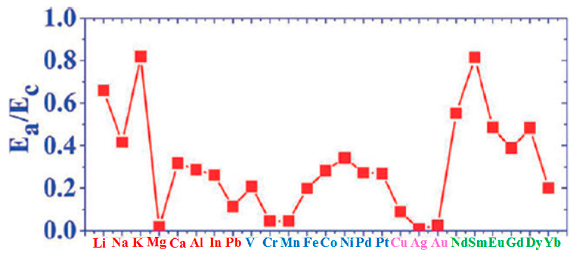
Figure 3.
Stable geometries of Au clusters adsorbed on perfect graphene. Au1–Au5 and Au5(P) clusters are shown from top to bottom rows. Left and right columns show top and side views, respectively. Reproduced from Reference [92] with permission from the American Physical Society.
Figure 3.
Stable geometries of Au clusters adsorbed on perfect graphene. Au1–Au5 and Au5(P) clusters are shown from top to bottom rows. Left and right columns show top and side views, respectively. Reproduced from Reference [92] with permission from the American Physical Society.
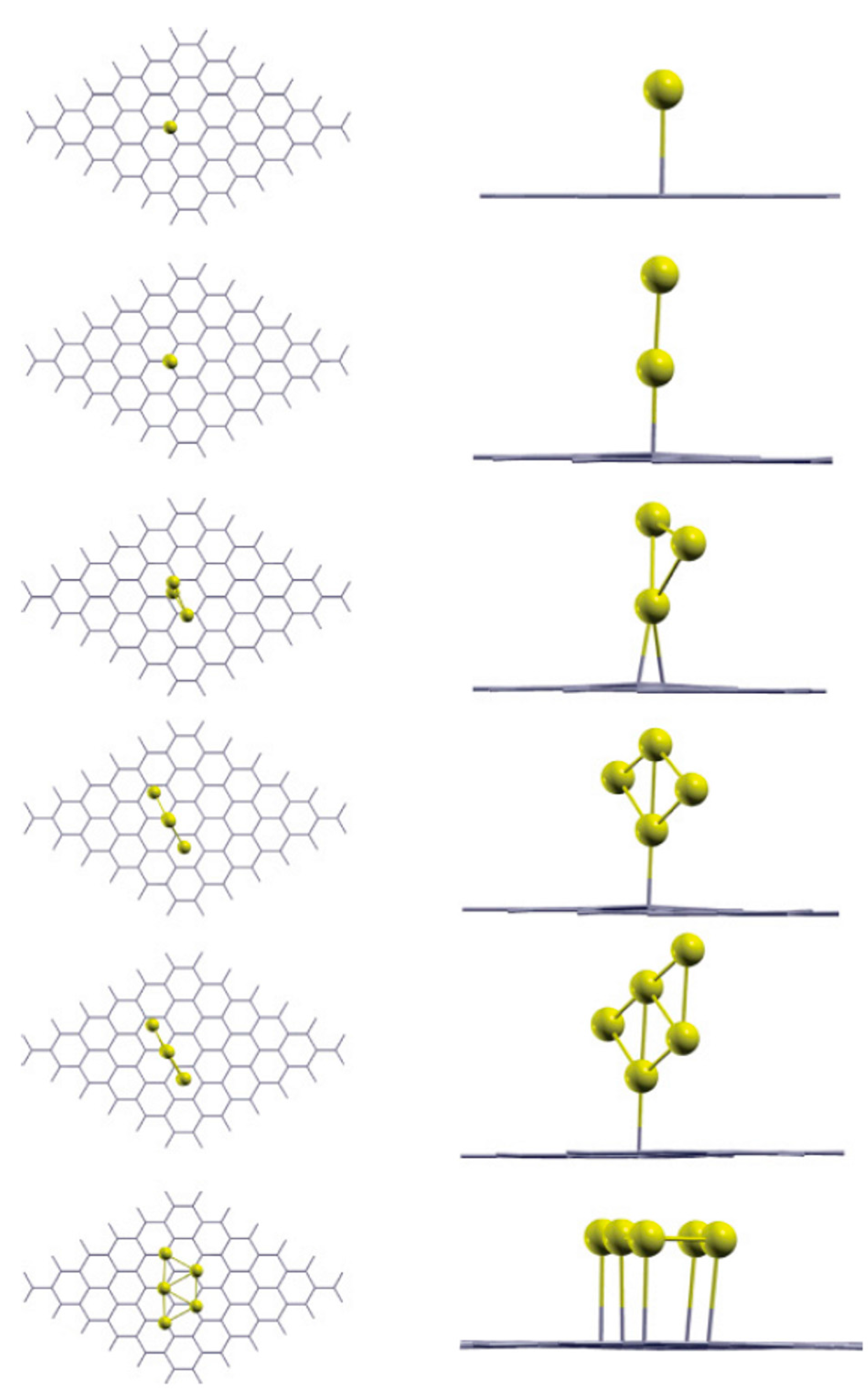
Figure 4.
Structures of the (3 × 3) surfaces used for the simulations: (a) freestanding graphene; (b) graphene on fcc Ru(0001); (c) graphene on hcp Ru(0001); and (d) graphene on ridge Ru(0001). Graphene is shown as bonds only. Top and second layer Ru atoms are shown as green and grey spheres, respectively. Reproduced from Reference [99] with permission from the American Institute of Physics.
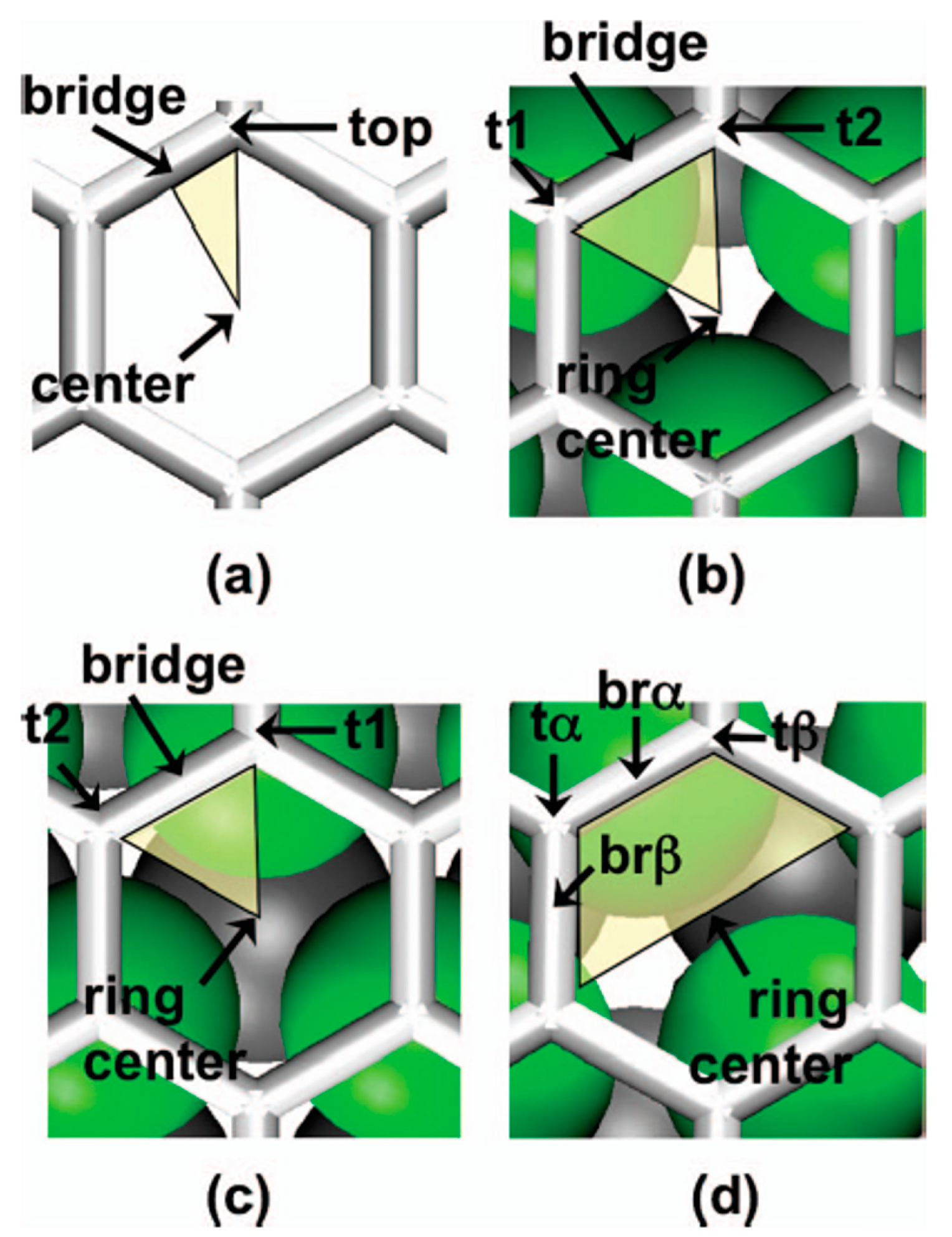
Figure 5.
Potential energy surfaces for Au1 on the (3 × 3) surfaces: (a) freestanding graphene; (b) graphene on fcc Ru(0001); (c) graphene on hcp Ru(0001); and (d) graphene on ridge Ru(0001). The hexagon identifies the standard graphene hexagon. In each image, the dashed line signs the adatom minimum-energy diffusion path. “X” marks the transition state from a local minimum energy site to another. The energy scale is in eV. Reproduced from Reference [99] with permission from the American Institute of Physics.
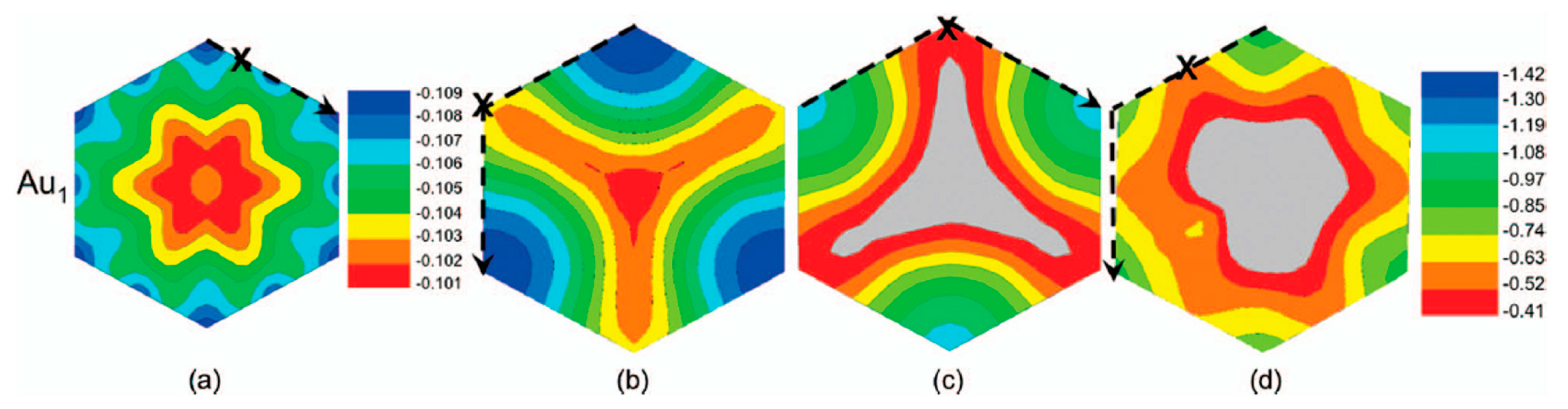
Figure 6.
Potential energy surfaces for Au1 sampled at the top and ring center sites in the symmetry-irreducible zone of the full graphene/Ru(0001) surface. The dashed line signs the adatom minimum-energy diffusion path. The minimum energy diffusion path for the adatom is marked by a dashed line. “D”, “E”, and “F” mark the preferential adsorption sites, and “X” marks the highest-energy site. Reproduced from Reference [99] with permission from the American Institute of Physics.

Figure 7.
Carbon vacancies formation energy in graphene (empty squares), and formation energies for Au adsorbed in graphene vacancies (full points). For each vacancy, the insets show the selected geometry for the vacancy. Reproduced from Reference [98] with permission from the American Institute of Physics.

Figure 8.
Au in double vacancies in graphene: simulations of different diffusion paths (path I, II, III, IV) of the Au atom (yellow sphere), whereas the blue dots indicate the C atoms which change position as result of the Au atom jump. In addition, each path is accompanied by the estimated diffusion barrier for the Au jump. Reproduced from Reference [98] with permission from the American Institute of Physics.

Figure 9.
Scanning Tunneling Microscopy images (50 nm × 50 nm) of (a) 0.05 ML; (b) 0.1 ML; (c) 0.2 ML; (d) 0.4 ML; (e) 0.6 ML and (f) 0.8 ML Rh deposited on graphene/Ru(0001) at room temperature. Reproduced from Reference [65] with permission from the Elsevier.
Figure 9.
Scanning Tunneling Microscopy images (50 nm × 50 nm) of (a) 0.05 ML; (b) 0.1 ML; (c) 0.2 ML; (d) 0.4 ML; (e) 0.6 ML and (f) 0.8 ML Rh deposited on graphene/Ru(0001) at room temperature. Reproduced from Reference [65] with permission from the Elsevier.

Figure 10.
Scanning Tunneling Microscopy images (50 nm × 50 nm) of (a) 0.1 ML Pd; (b) 0.4 ML Pd; (c) 0.2 ML Co; (d) 0.4 ML Co; (e) 0.2 ML Au and (f) 0.6 ML Au deposited on graphene/Ru(0001) at room temperature. Reproduced from Reference [65] with permission from the Elsevier.
Figure 10.
Scanning Tunneling Microscopy images (50 nm × 50 nm) of (a) 0.1 ML Pd; (b) 0.4 ML Pd; (c) 0.2 ML Co; (d) 0.4 ML Co; (e) 0.2 ML Au and (f) 0.6 ML Au deposited on graphene/Ru(0001) at room temperature. Reproduced from Reference [65] with permission from the Elsevier.
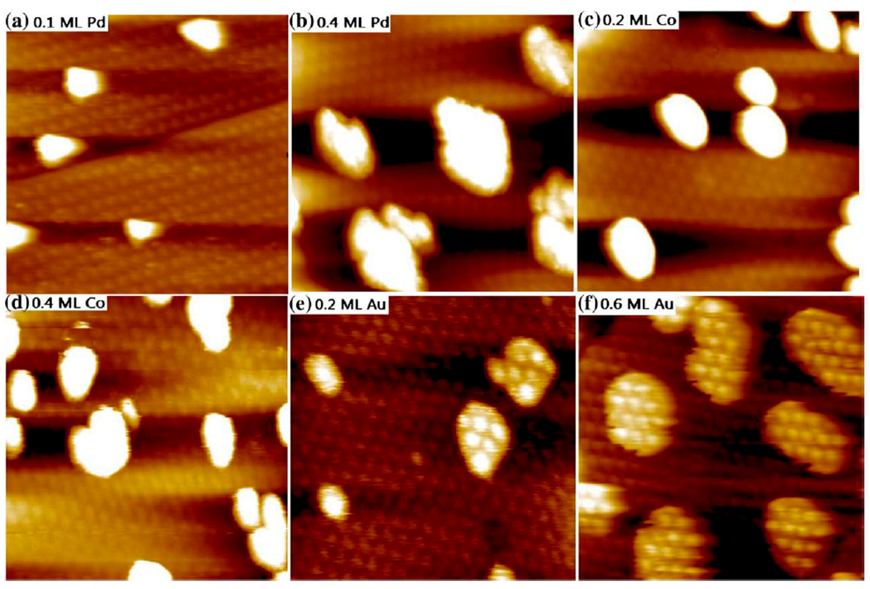
Figure 11.
Scanning Tunneling Microscopy images (50 nm × 50 nm) of 0.8 ML Rh on graphene/Ru(0001) acquired after annealing the samples to (a) 600 K; (b) 700 K; (c) 800 K; (d) 900 K; (e) 1000 K and (f) 1100 K for 10 min. Reproduced from Reference [65] with permission from the Elsevier.
Figure 11.
Scanning Tunneling Microscopy images (50 nm × 50 nm) of 0.8 ML Rh on graphene/Ru(0001) acquired after annealing the samples to (a) 600 K; (b) 700 K; (c) 800 K; (d) 900 K; (e) 1000 K and (f) 1100 K for 10 min. Reproduced from Reference [65] with permission from the Elsevier.
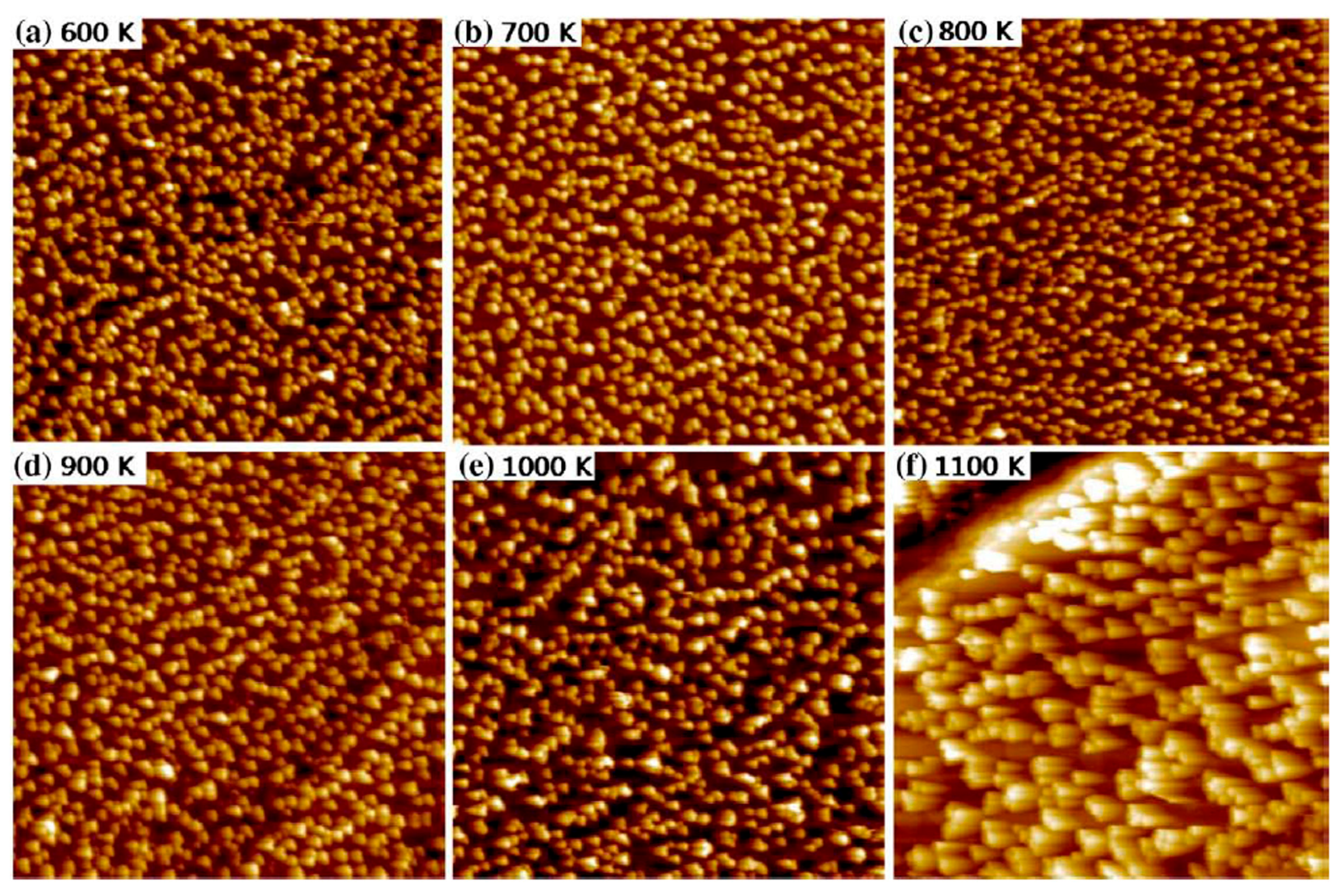
Figure 12.
Scanning Tunneling Microscopy images (70 nm × 70 nm) of graphene flakes on Ir(111) after deposition, maintaining the substrate at 300 K, of: (a) 0.20 ML Ir; (b) 0.25 ML Pt; (c) 0.44 ML W; (d) 0.53 ML Re; (e) 0.77 ML Fe; (f) 0.25 ML Au. Reproduced from Reference [64] with permission from IOPscience.
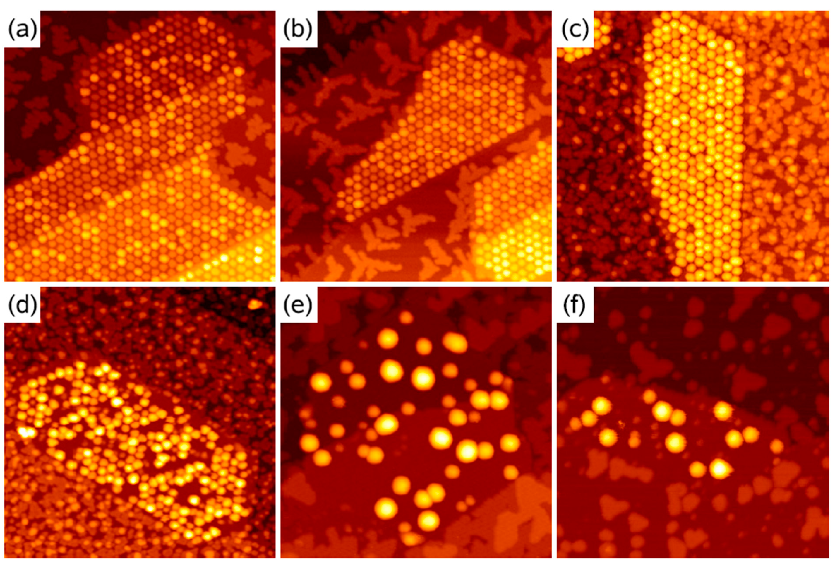
Figure 13.
Scanning Tunneling Microscopy images (70 nm × 70 nm) of (a) 0.25 ML Pt deposited on graphene/Ir(111) maintaining the substrate at 300 K. This sample was then annealed for 300 s at (b) 400 K; (c) 450 K (d) 500 K; (e) 550 K and (f) 650 K; (g) Plot of n (occupation probability of the moiré cell by a particle) versus the annealing temperature T; (h) Arrhenius plot of particle jumping rate ν(T). Lines represent fits for the hopping rate with diffusion parameters as shown in Table 3. Reproduced from Reference [64] with permission from IOPscience.
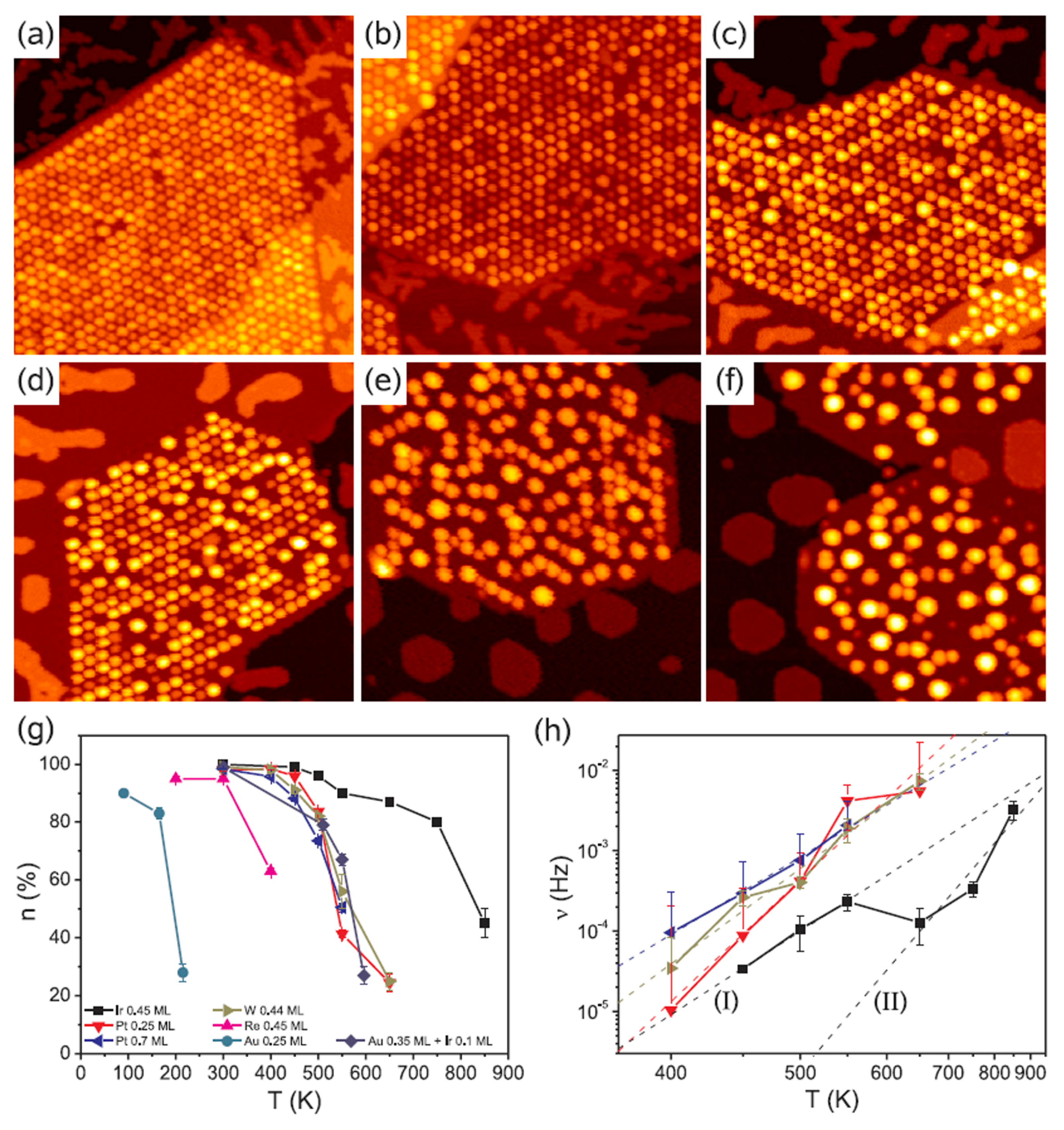
Figure 14.
(a–e) Scanning Tunneling Microscopy images (25 nm × 25 nm) of 0.01 ML Ir deposited at 350 K on graphene/Ir(111) (a) and annealed at 390 K for 120 s (b); 240 s (c); 360 s (d); 480 s (e). Circles indicate where modification occur in successive images; (f–j) Scanning Tunneling Microscopy images (15 nm × 15 nm) of 1.5 ML Ir deposited on graphene/Ir(111) at 350 K (f) and annealed at 450 K for 120 s (g); 240 s (h); 360 s (i); 480 s (j). Reproduced from Reference [64] with permission from IOPscience.
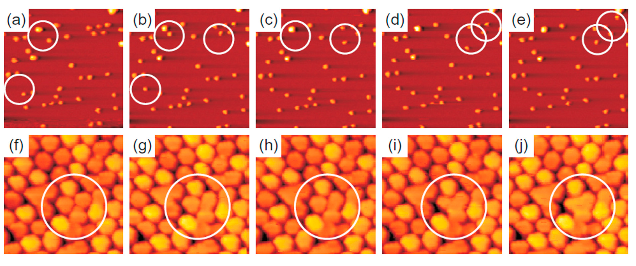
Figure 15.
(a–d) Transmission Electron Microscopy images of Au deposited on free-standing graphene increasing the amount of deposited metal; (a) Sparse coverage; (b) sparse groups of clusters at Au thickness lower than 0.1 nm; (c) Higher cluster densities at 0.12 nm of Au thickness; (d) Coalescence of clusters occurring for 2.12 nm-thick deposited Au; (e) Scanning Transmission Electron Microscopy bright-field image of 0.5 nm-thick evaporated Au. Scale bar: 10 nm in all images. Reproduced from Reference [66] with permission from Wiley.
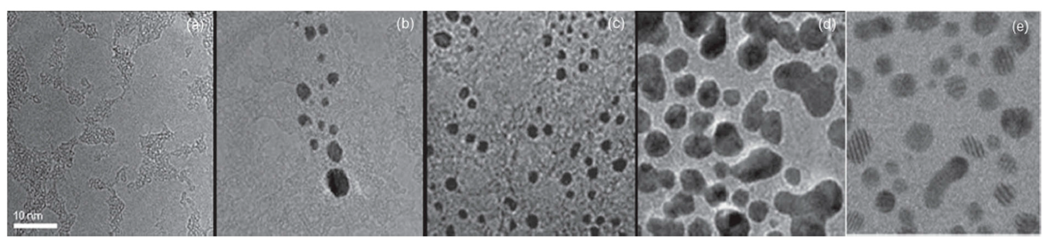
Figure 16.
Coalesced Au clusters corresponding to the deposition of 2.12 nm Au on graphene. (a) shows variations in thickness and relative crystallographic orientations and (b) planar faults such as stacking faults (white arrows) and twin boundaries (black arrow). Scale bars: 5 nm. Reproduced from Reference [66] with permission from Wiley.

Figure 17.
(a,b): Transmission Electron Microscopy images of 0.2 nm Au evaporated onto hydrogenated and pristine graphene (scale bar: 20 nm). The corresponding diffraction patterns are shown as insets; (c,d) Images of Au evaporated onto hydrogenated graphene, taken in a sequence of scans, and showing the Au clusters merging by coalescence as indicated by the solid circles and dashed rectangles (scale bar: 5 nm). Reproduced from Reference [66] with permission from Wiley.
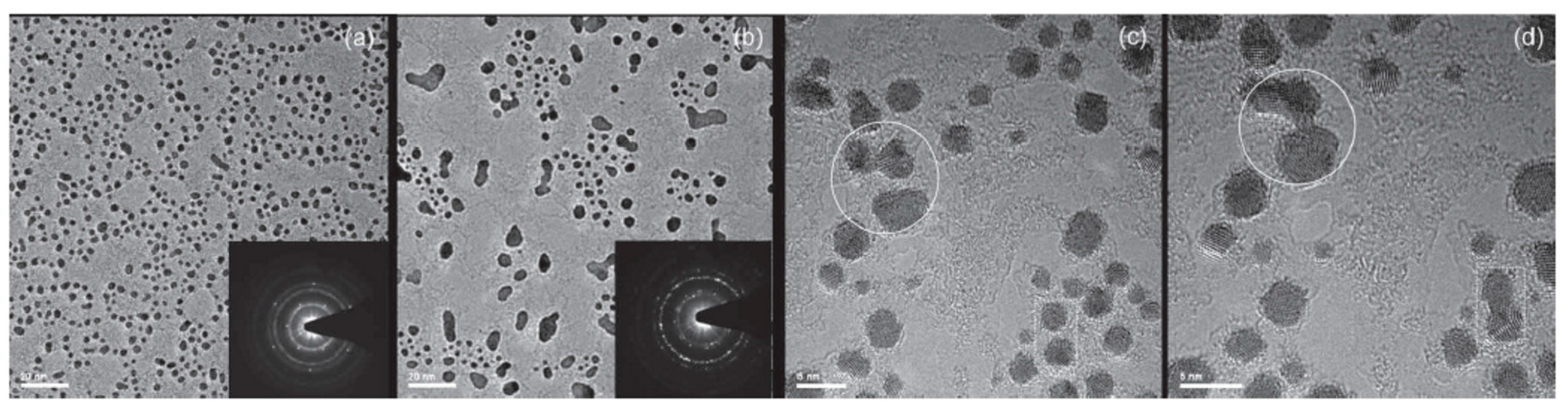
Figure 18.
(a,b) Plan-view Transmission Electron Microscopy images of Pt atoms in a four-layer graphitic sheet held at 600 °C. The image (b) was acquired 60 s after (a). Two Pt atoms (arrowed) merge and form a cluster. The scale bar is 1 nm. Reproduced from Reference [58] with permission from Wiley.

Figure 19.
Series of Transmission Electron Microscopies showing the diffusion of Pt atoms in graphene at 600 °C as a function of time. “L” marks the region in a two-three layer graphene where Pt atoms are diffusing in two dimensions. “E” marks a Pt cluster located at the edge of a graphene layer and where Pt atoms are observed one-dimensionally diffuse along the edge. Reproduced from Reference [58] with permission from Wiley.
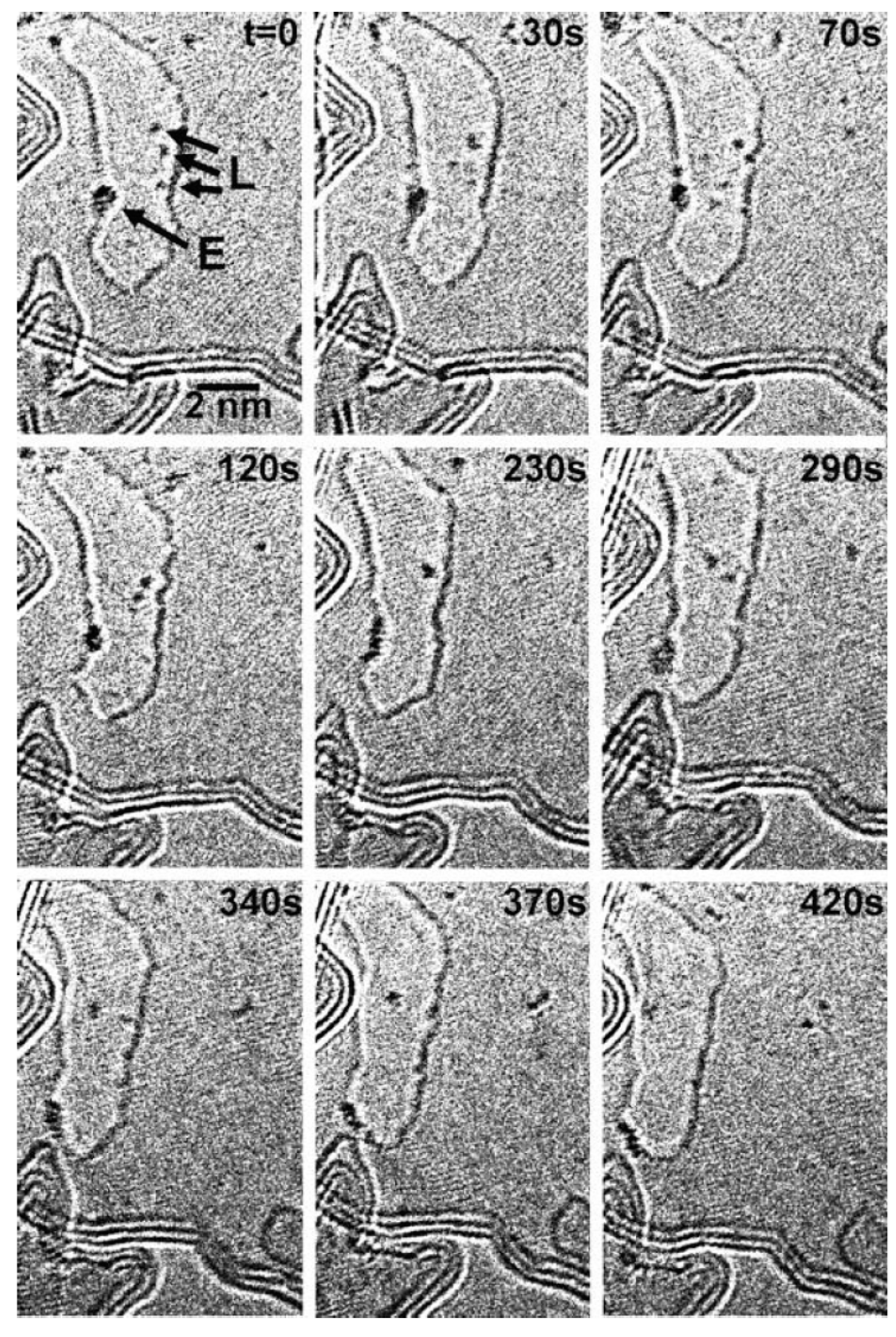
Figure 20.
Atomic Force Microscopy images (1 μm × 1 μm) of 0.1 nm Au deposited on a single-layer graphene (a) and on graphite (b). (c,d) show the same samples (Au on single-layer graphene in (c) and Au on graphite in (d)) after 2 h of thermal annealing at 350 °C. Reproduced from Reference [60] with permission from the American Chemical Society.
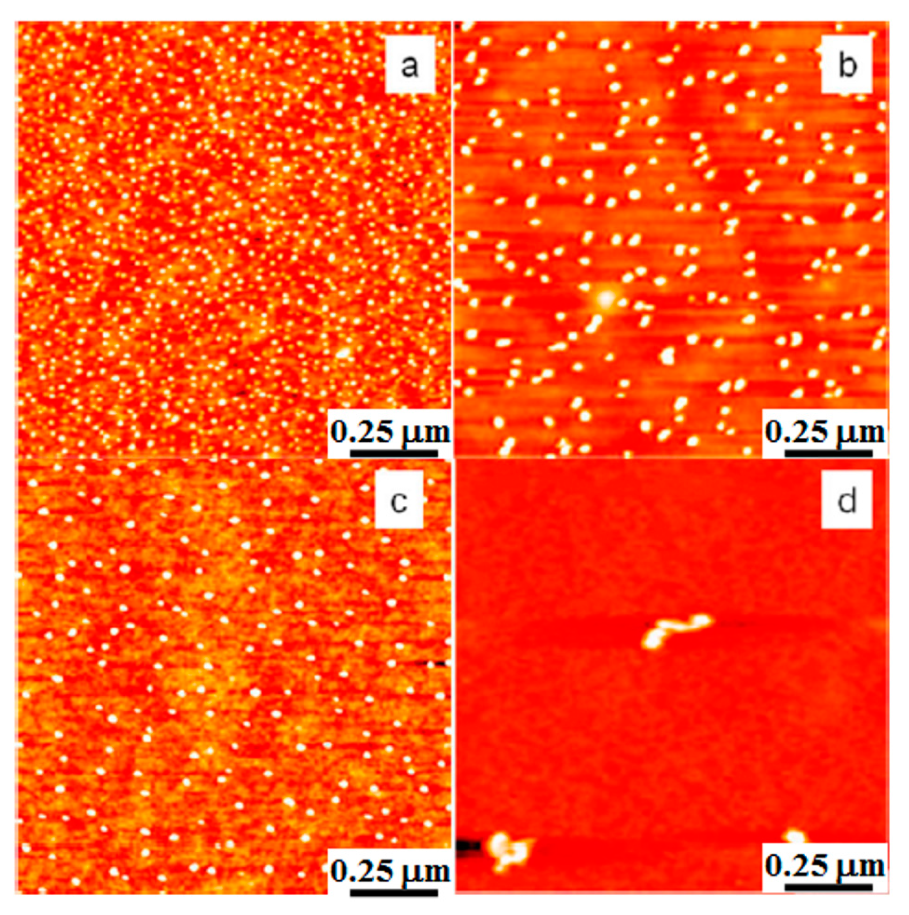
Figure 21.
(a) Atomic Force Microscopy images (1 μm × 1 μm) of 1 layer graphene on hexagonal boron nitride (h-BN); and (b) Atomic Force Microscopy images (1 μm × 1 μm) of 0.1 nm Au deposited on 1 layer graphene supported on h-BN; (c) Atomic Force Microscopy images (1 μm × 1 μm) of 0.1 nm Au deposited directly on h-BN; (d) Atomic Force Microscopy images (1 μm × 1 μm) of 0.1 nm Au deposited on bilayer graphene supported on SiO2. Reproduced from Reference [60] with permission from the American Chemical Society.
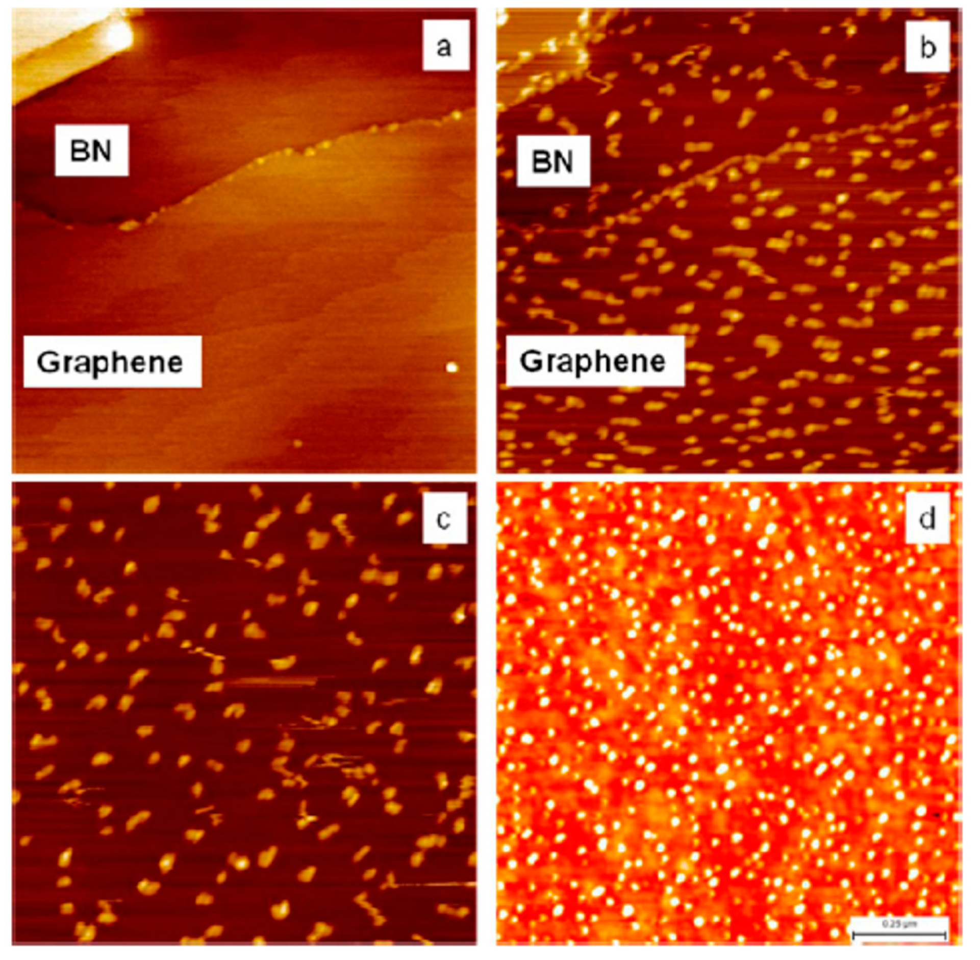
Figure 22.
The calculated diffusion energy, Ed, and diffusion constant, D, of Au adatoms on various surfaces: graphite, hexagonal boron nitride (h-BN), single-layer graphene (SLG) on h-BN, SLG on SiO2, and bilayer graphene (BLG) on SiO2. Calculations using different critical sizes i are given in black (i = 1) and red (i = 2) curves for comparison. For graphite, Ed and D are assumed as 50 meV and 7 × 10⁻⁶ cm2 s−1, independent of critical size i. Reproduced from Reference [60] with permission from the American Chemical Society.
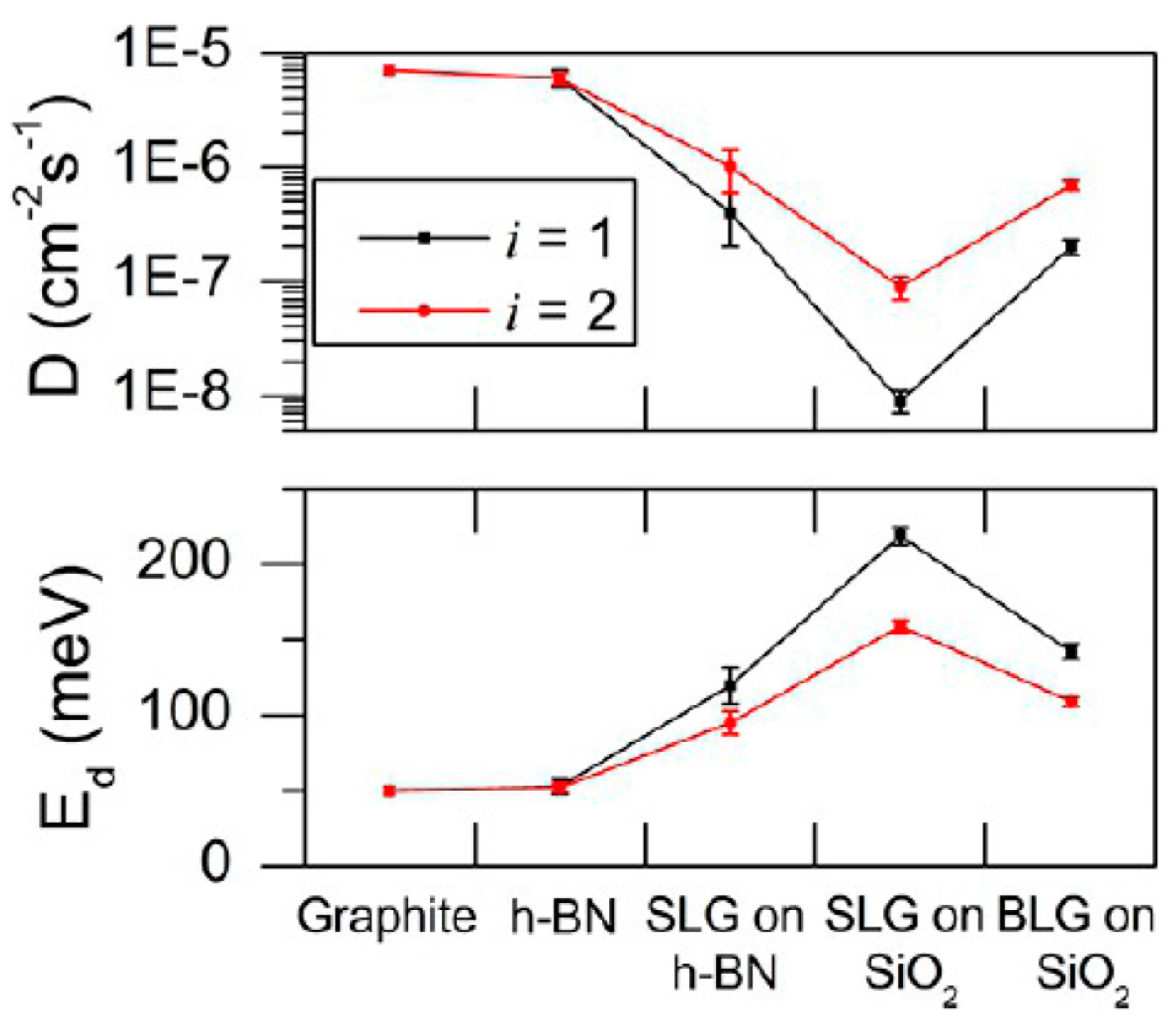
Figure 23.
Scanning Electron Microscopy images showing the dewetting of Au films into hexagonal Au NPs on graphene after thermal annealing at 700 °C for 2 h. Film thickness: 2.0 nm. Scale bar: 200 nm. (a) Hexagonal Au NPs on SiO2 (left) and monolayer graphene (right); (b) Hexagonal Au NPs on SiO2 (left) and bilayer graphene (right); (c) Hexagonal Au NPs on trilayer graphene (left) and SiO2 (right); (d) Hexagonal Au NPs on bilayer (left) and four layer graphene (right). Reproduced from Reference [68] with permission from Elsevier.

Figure 24.
Scanning Electron Microscopy images showing the effects of the starting thickness of the deposited Au film on the shape of the resulting NPs after the annealing process at 600 °C for 2 h. Scale bar: 200 nm. (a,b) 1.0 nm thick Au; (c,d) 1.5 nm thick Au; (e,f) 2.0 nm thick Au. It is obvious to find that with the increase of Au film thickness, the modulation becomes less effective. Reproduced from Reference [68] with permission from Elsevier.

Figure 25.
Morphologies, size, and density of Au nanoparticles on n-layer graphenes after annealing at 1260 °C in vacuum for 30 s (false-color image). Note that no Au NPs are found in the substrate. (a) Au NPs on monolayer, bilayer, and trilayer graphene, respectively; (b) Statistics of the size and density of gold nanoparticles on n-layer graphenes. Reproduced from Reference [69] with permission from the American Chemical Society.

Figure 26.
Scanning Electron Microscopy images (1 μm scale bar) of monolayer and bilayer graphene on SiO2 after deposition of 5 nm Ag maintaining the substrate at different temperature during the deposition: (a,b) 298 K; (c,d) 333 K; (e,f) 373 K. Reproduced from Reference [71] with permission from the American Chemical Society.
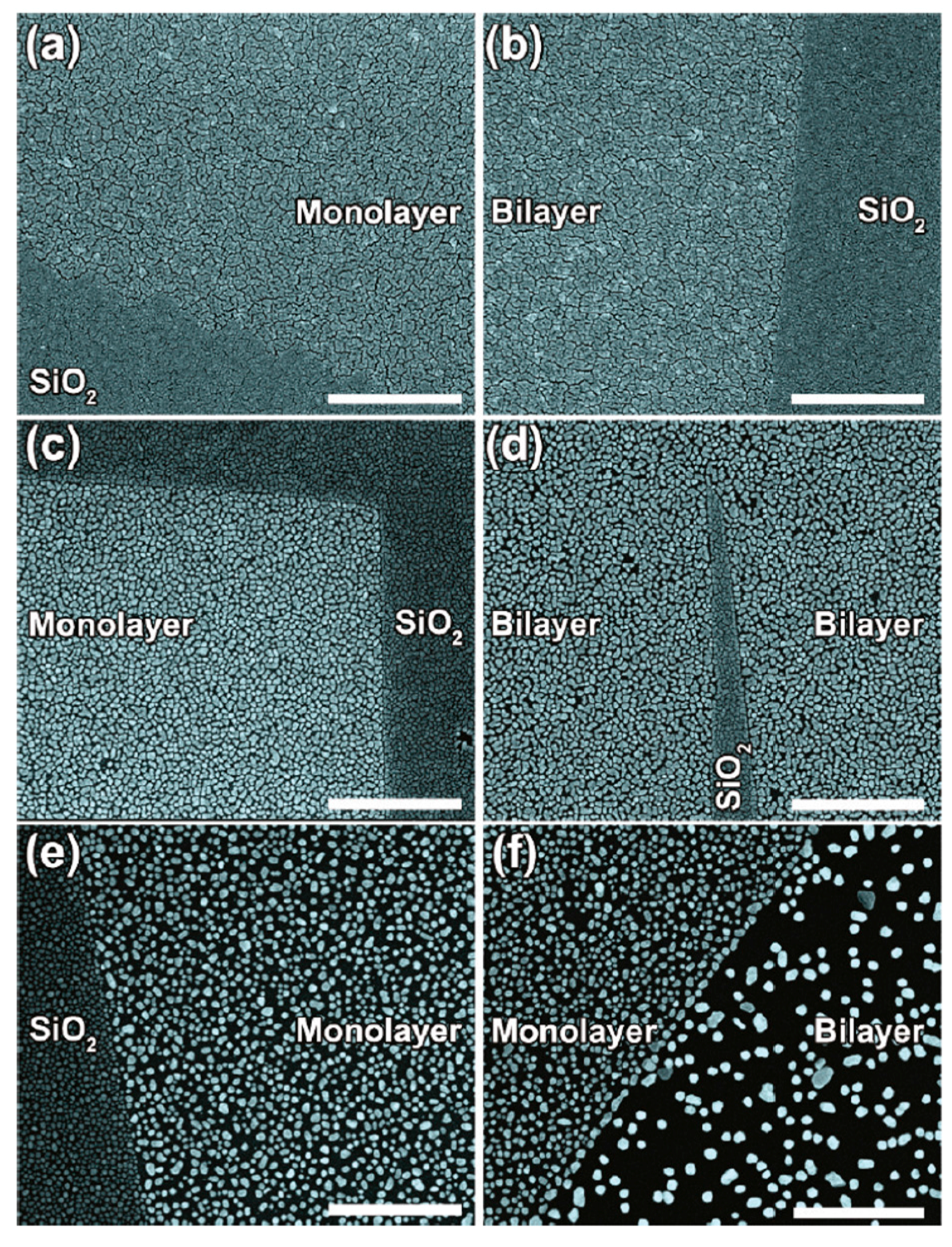
Figure 27.
Raman spectra from monolayer and bilayer graphene on SiO2 having deposited on the graphene 2 or 5 nm Ag film. Reproduced from Reference [71] with permission from the American Chemical Society.
Figure 27.
Raman spectra from monolayer and bilayer graphene on SiO2 having deposited on the graphene 2 or 5 nm Ag film. Reproduced from Reference [71] with permission from the American Chemical Society.

Figure 28.
Raman spectra of monolayer (a) and bilayer (b) graphene covered by 5 nm Ag deposited maintaining the substrate at 298 K (black line), 333 K (red line), and 373 K (blue line). Reproduced from Reference [71] with permission from the American Chemical Society.
Figure 28.
Raman spectra of monolayer (a) and bilayer (b) graphene covered by 5 nm Ag deposited maintaining the substrate at 298 K (black line), 333 K (red line), and 373 K (blue line). Reproduced from Reference [71] with permission from the American Chemical Society.
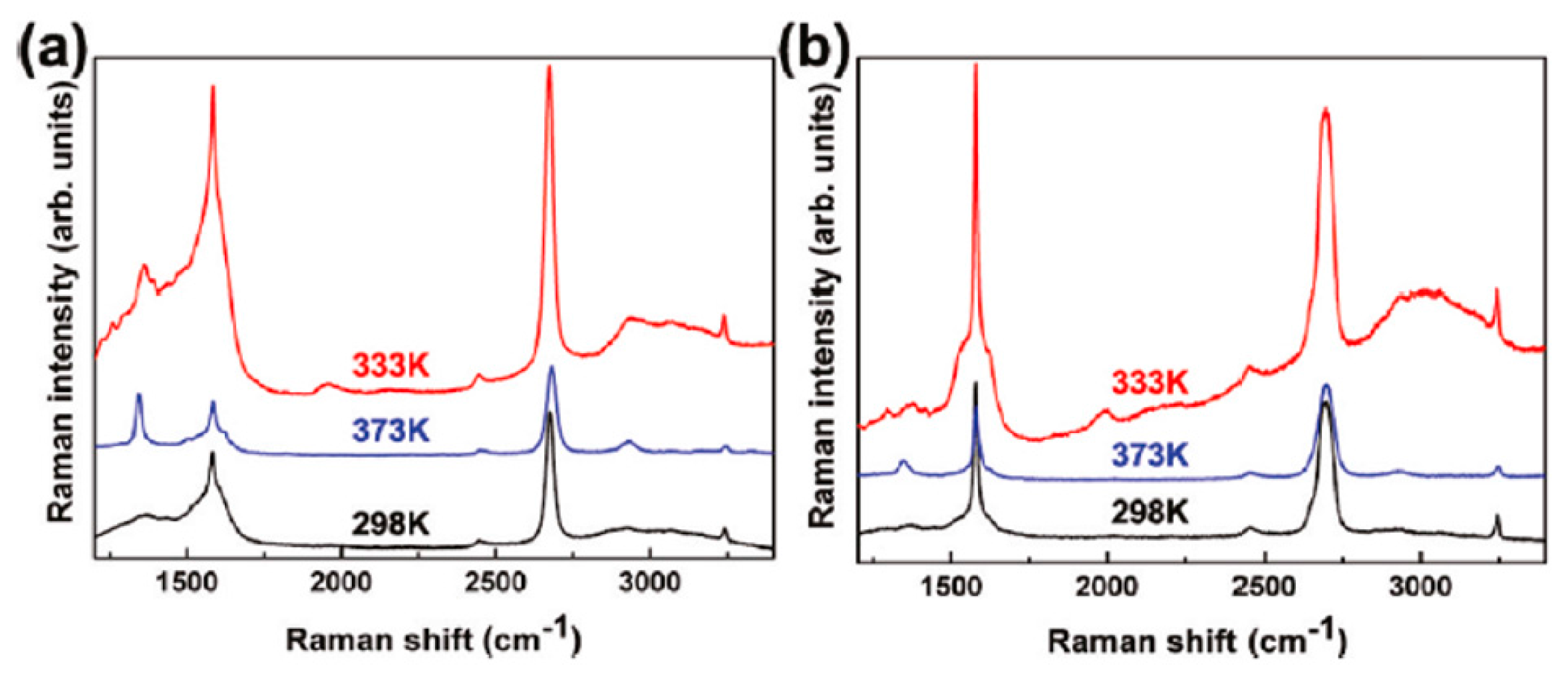
Figure 29.
Metal-graphene contact resistance versus metal work-function. The square indicates the mean value. Reproduced from Reference [105] with permission from Elsevier.
Figure 29.
Metal-graphene contact resistance versus metal work-function. The square indicates the mean value. Reproduced from Reference [105] with permission from Elsevier.

Figure 30.
Schematic picture of metal contact to graphene. (a,b) indicate a schematic model of the metal/graphene junction for the large and small contact resistance values, respectively. The model shows that the contact resistance becomes smaller with increasing contact area between the metal grain and the graphene. Reproduced from Reference [105] with permission from Elsevier.
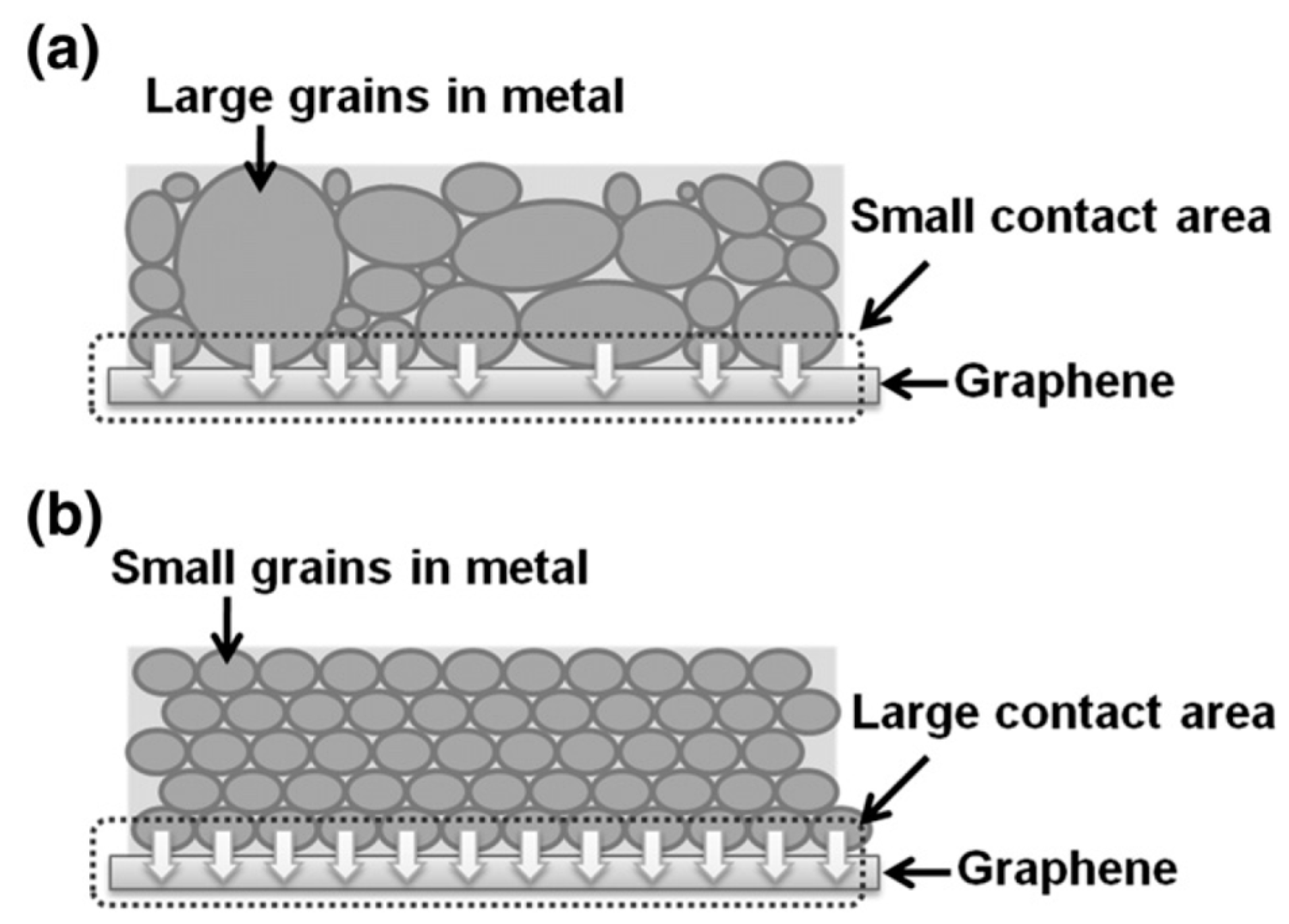

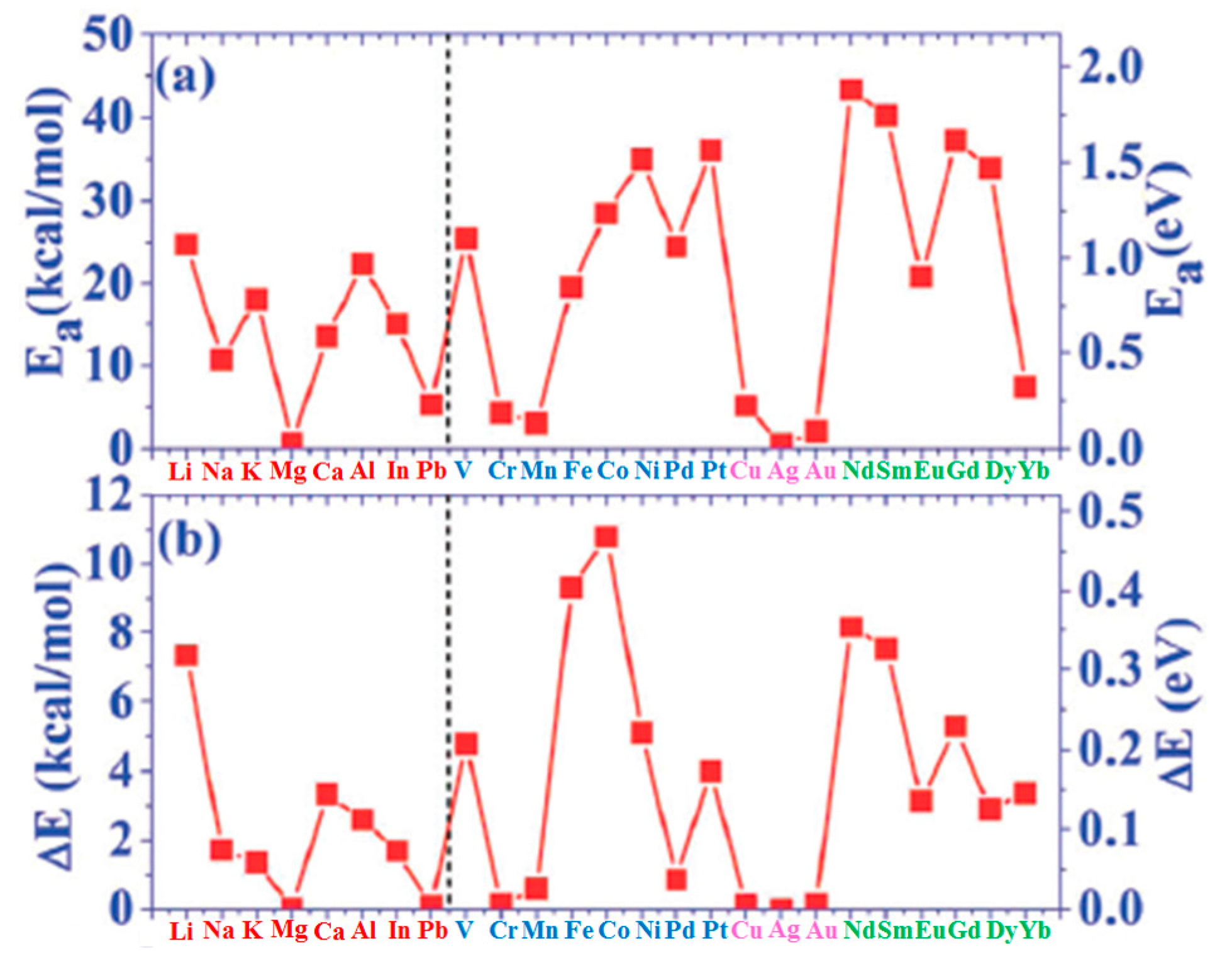
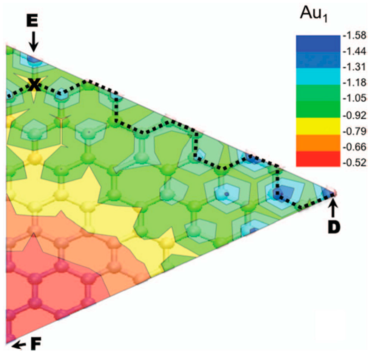
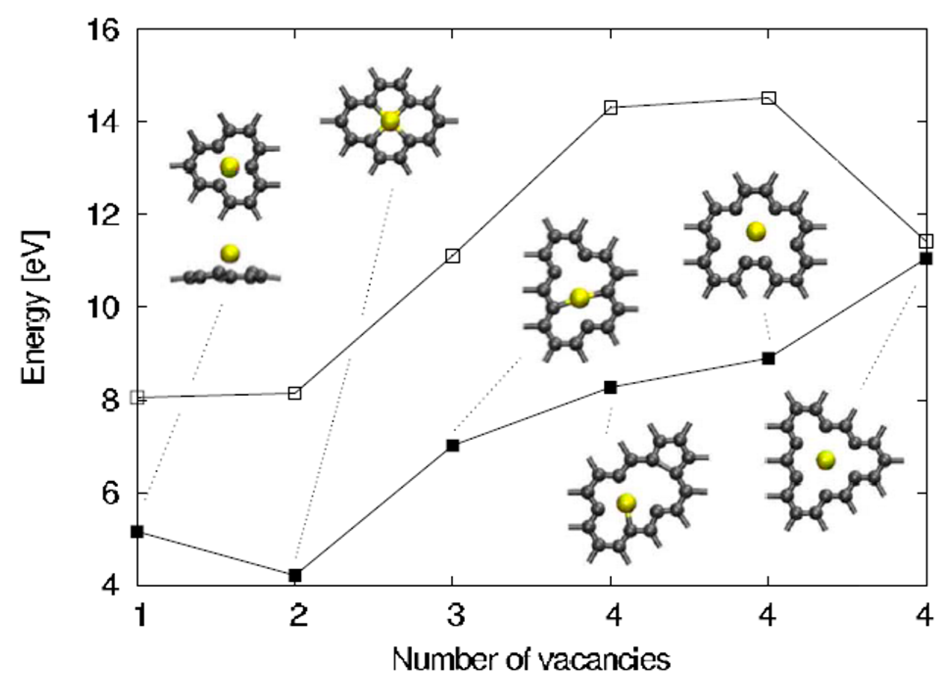
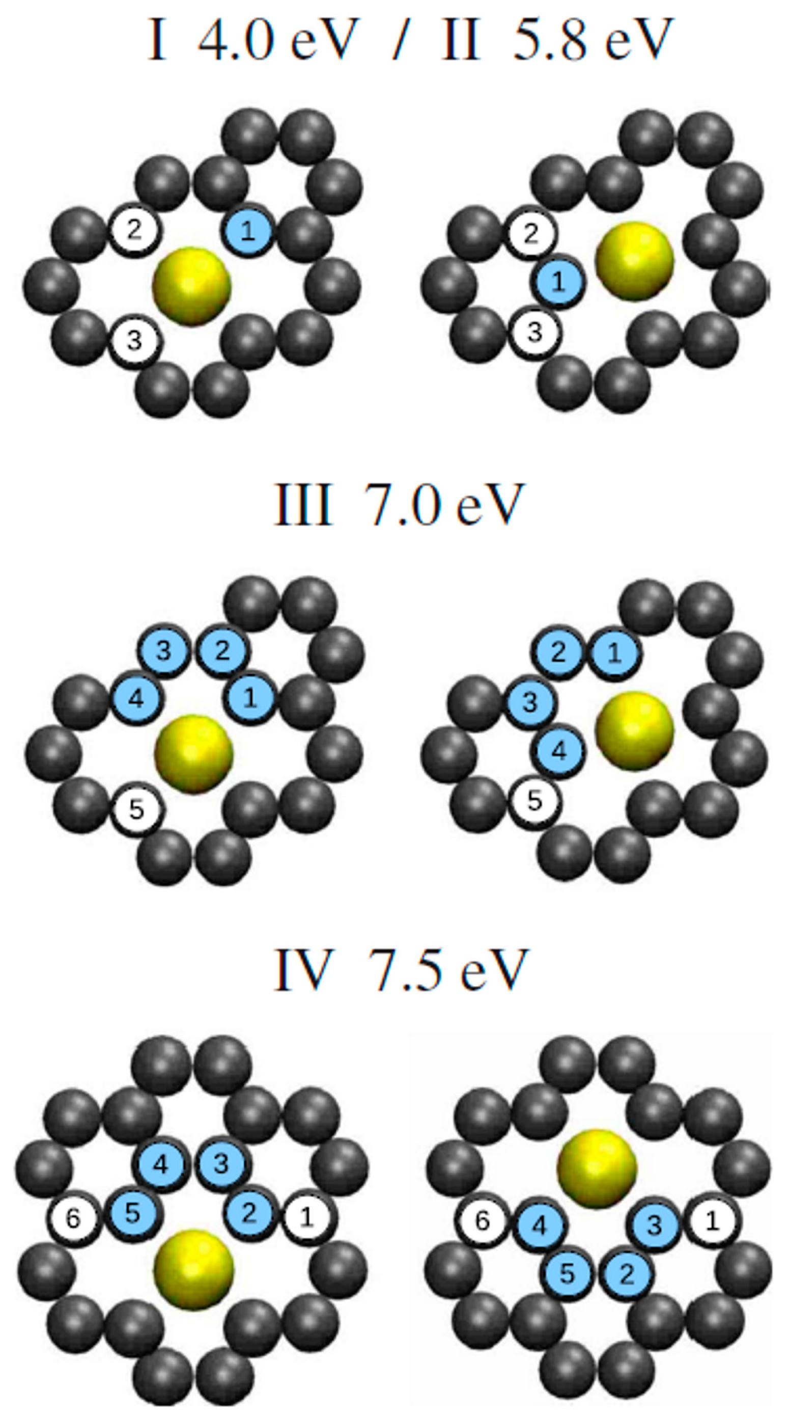
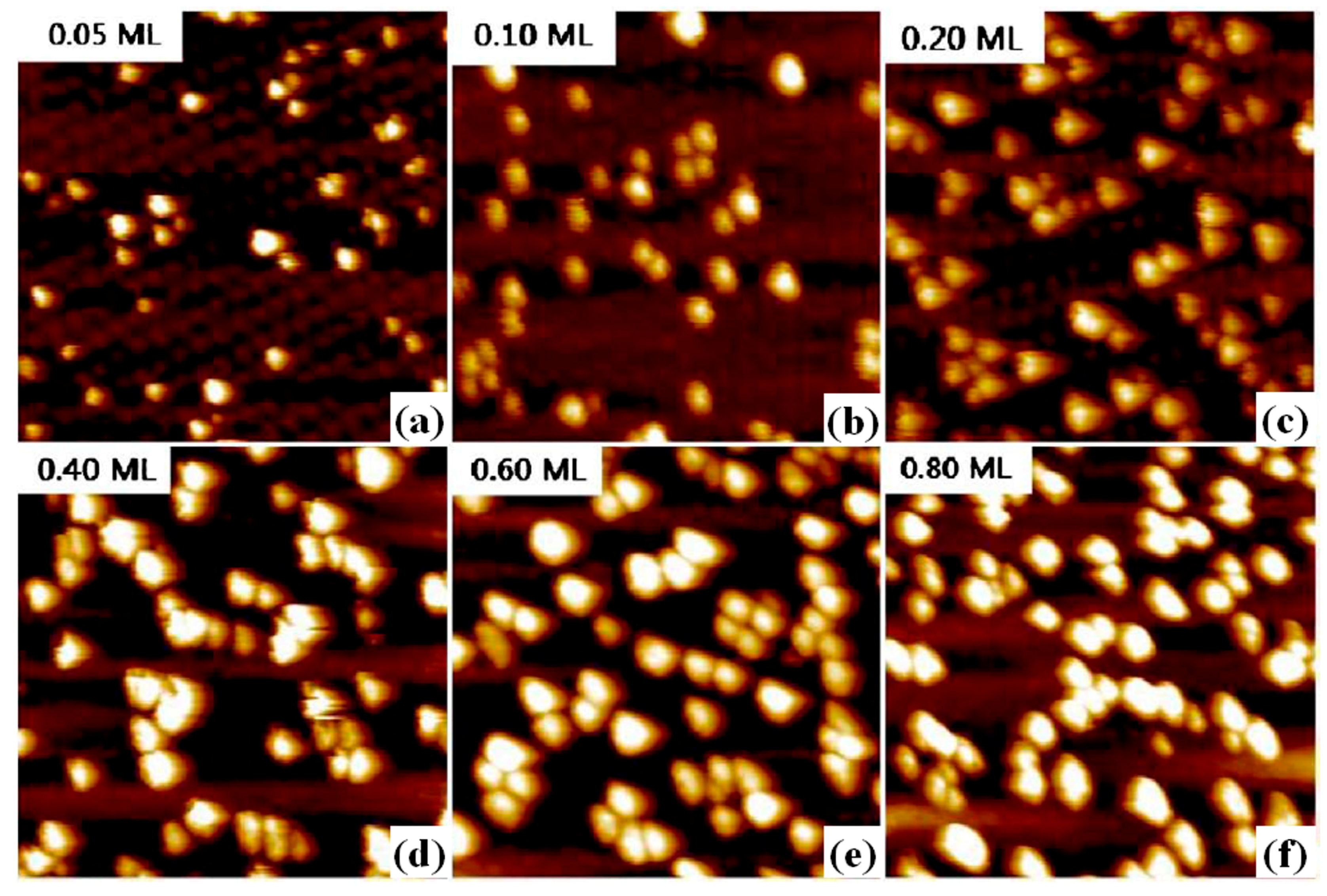
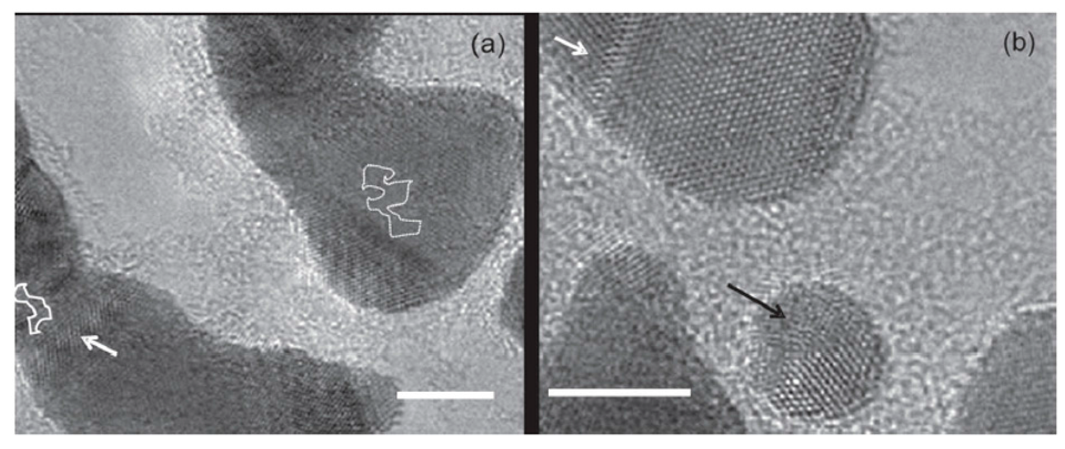
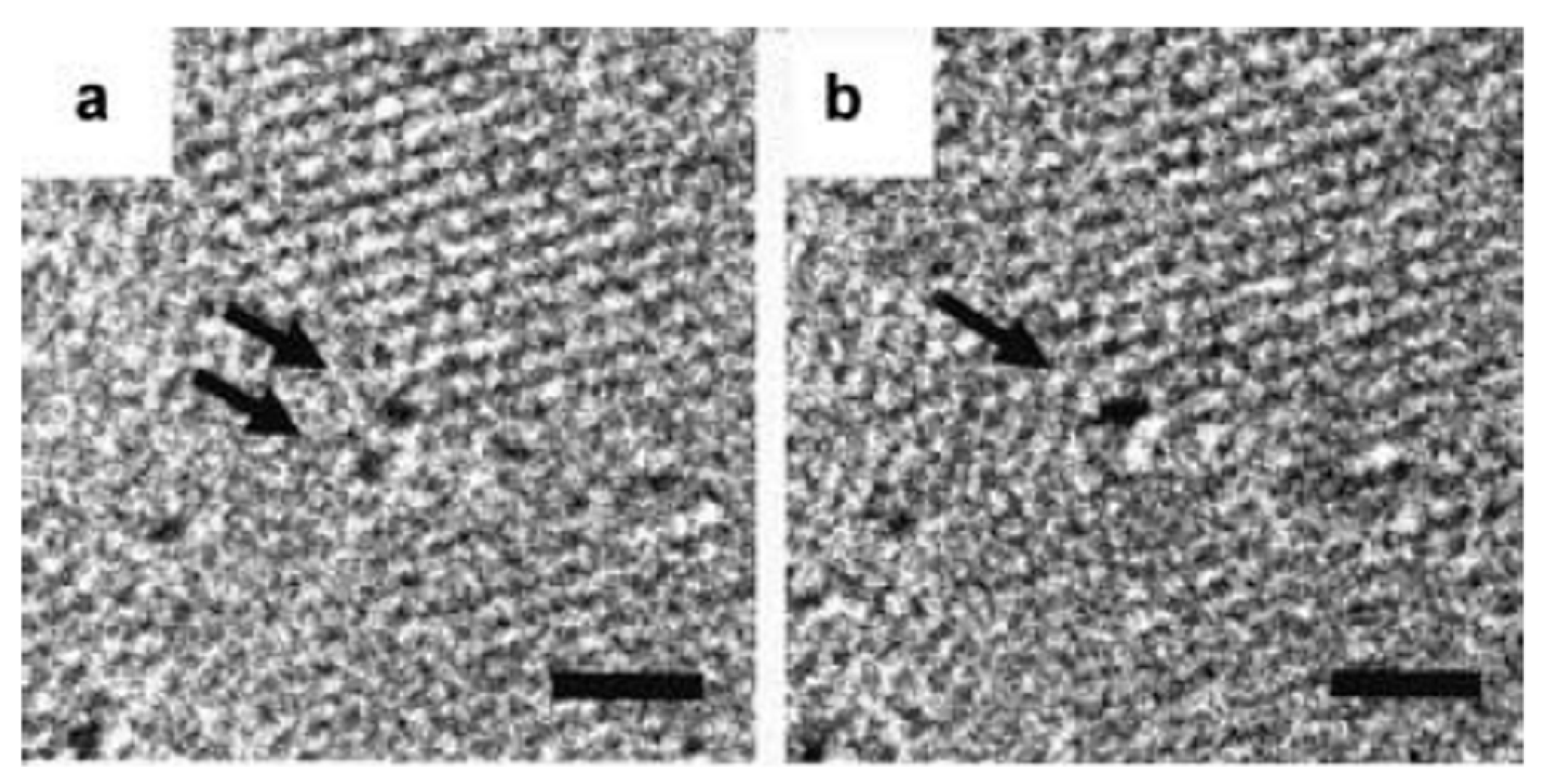
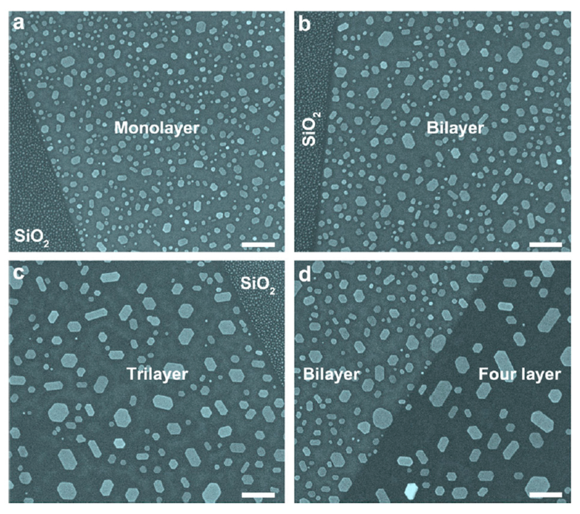
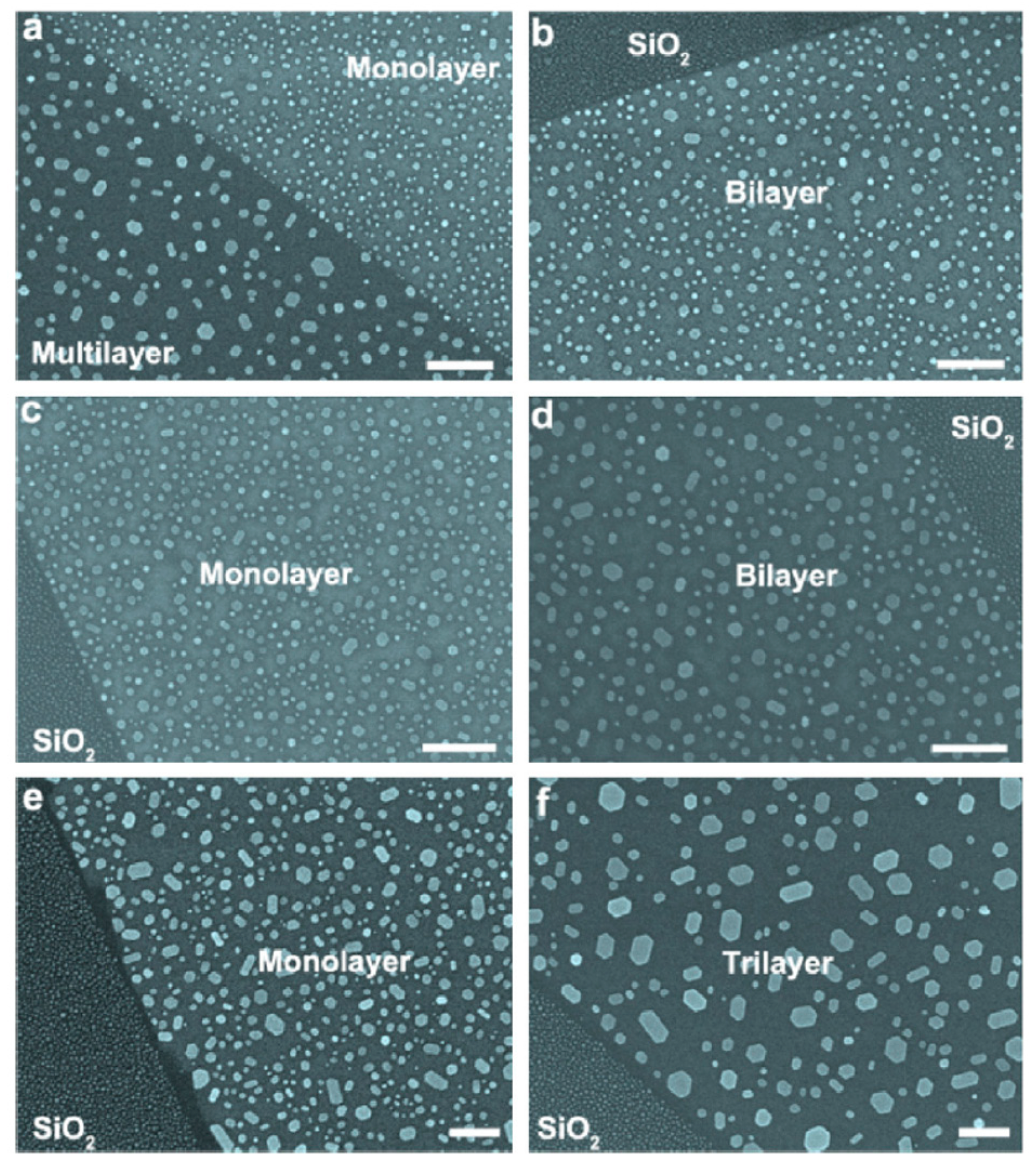
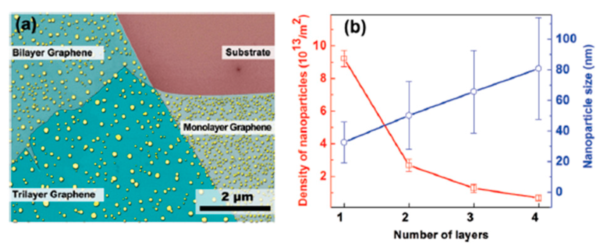
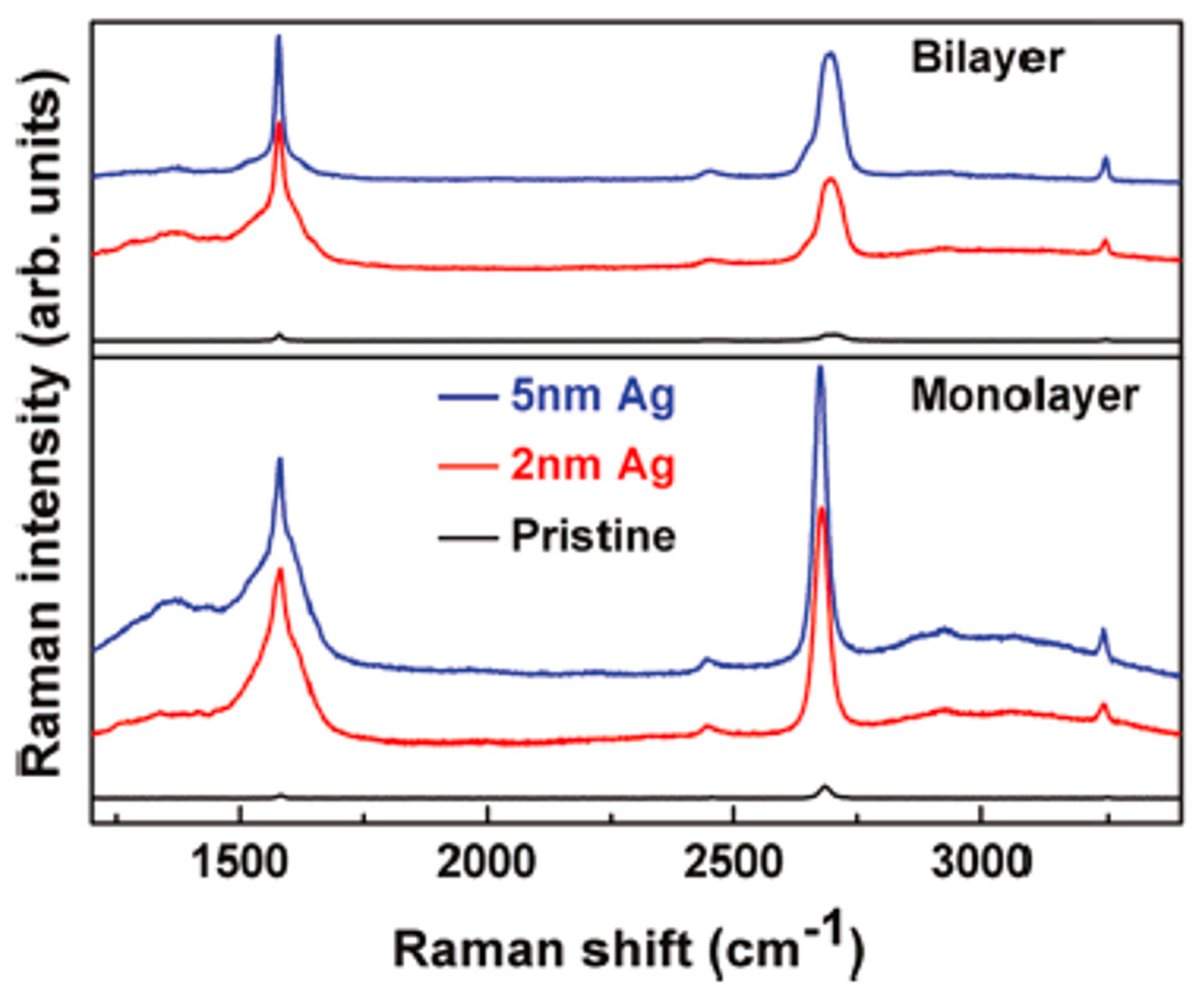
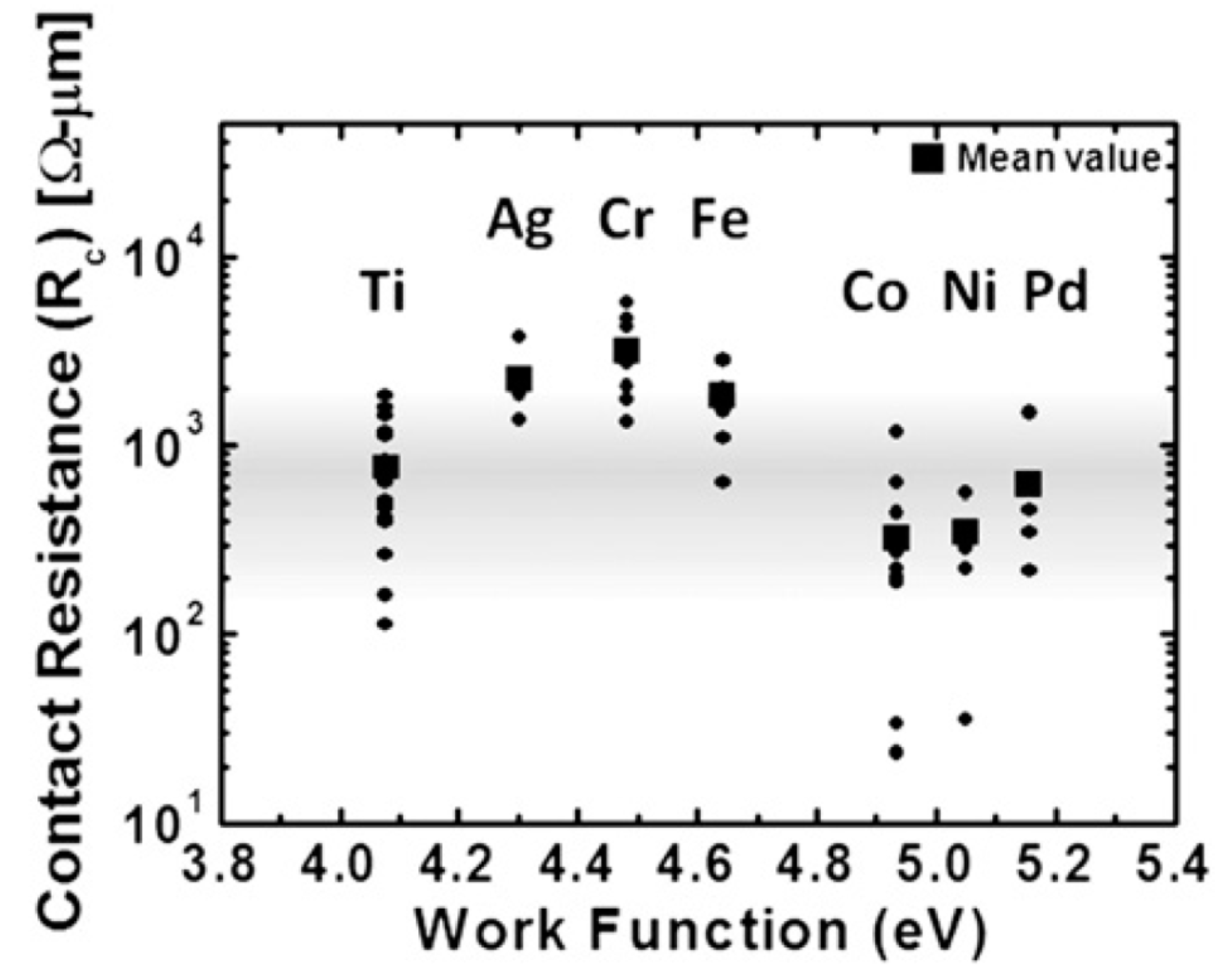
Table 1.
Ea (adsorption energy of the metal atom on graphene, kcal/mol), ΔE (diffusion barrier of the metal adatom on graphene, kcal/mol), Ea/Ec (with Ec the bulk metal cohesive energy), and Ec−Ea (kcal/mol). Reproduced from Reference [100] with permission from the Royal Society of Chemistry.
Table 1.
Ea (adsorption energy of the metal atom on graphene, kcal/mol), ΔE (diffusion barrier of the metal adatom on graphene, kcal/mol), Ea/Ec (with Ec the bulk metal cohesive energy), and Ec−Ea (kcal/mol). Reproduced from Reference [100] with permission from the Royal Society of Chemistry.
| Adatoms | Sites | Ea | ΔE | Ea/Ec | Ec−Ea |
|---|---|---|---|---|---|
| Li | H | 24.77 | 7.33 | 0.659 | 12.82 |
| Na | H | 10.70 | 1.71 | 0.417 | 14.97 |
| K | H | 18.10 | 1.36 | 0.818 | 4.036 |
| Mg | H | 0.65 | 0.02 | 0.019 | 34.18 |
| Ca | H | 13.44 | 3.34 | 0.317 | 28.99 |
| Al | H | 22.41 | 2.58 | 0.287 | 55.70 |
| In | H | 15.15 | 1.68 | 0.261 | 42.90 |
| Pb | T | 5.28 | 0.09 | 0.113 | 41.47 |
| V | H | 25.44 | 4.77 | 0.208 | 96.86 |
| Cr | B | 4.34 | 0.14 | 0.046 | 90.22 |
| Mn | H | 3.04 | 0.60 | 0.045 | 64.30 |
| Fe | H | 19.65 | 9.32 | 0.199 | 79.08 |
| Co | H | 28.53 | 10.79 | 0.282 | 72.65 |
| Ni | H | 35.01 | 5.12 | 0.342 | 67.37 |
| Pd | B | 24.47 | 0.85 | 0.273 | 65.24 |
| Pt | B | 36.09 | 3.99 | 0.268 | 98.59 |
| Cu | T | 5.17 | 0.12 | 0.090 | 52.26 |
| Ag | B | 0.51 | 0.00 | 0.007 | 67.53 |
| Au | T | 2.08 | 0.14 | 0.024 | 85.79 |
| Nd | H | 43.31 | 8.16 | 0.552 | 35.15 |
| Sm | H | 40.15 | 7.52 | 0.814 | 9.20 |
| Eu | H | 20.85 | 3.14 | 0.486 | 22.05 |
| Gd | H | 37.17 | 5.28 | 0.389 | 58.39 |
| Dy | H | 33.94 | 2.88 | 0.484 | 36.19 |
| Yb | H | 7.40 | 3.37 | 0.201 | 29.43 |
Table 2.
Anchor atom’s distance above graphene plane (ha), distance from nearest-neighbor C atom (dac), binding energies (BE1–BE3) of Aun clusters adsorbed on perfect graphene. Reproduced from Reference [92] with permission from the American Physical Society.
Table 2.
Anchor atom’s distance above graphene plane (ha), distance from nearest-neighbor C atom (dac), binding energies (BE1–BE3) of Aun clusters adsorbed on perfect graphene. Reproduced from Reference [92] with permission from the American Physical Society.
| System | ha (Å) | dac (Å) | BE1 (eV) | BE2 (eV) | BE3 (eV) |
|---|---|---|---|---|---|
| Au1 | 2.89 | 2.82 | −0.107 | −0.107 | −0.122 |
| Au2 | 2.45 | 2.32 | −1.373 | −2.639 | −0.526 |
| Au3 | 2.43 | 2.33 | −1.345 | −1.288 | −0.654 |
| Au4 | 2.49 | 2.34 | −1.608 | −2.397 | −0.515 |
| Au5 | 2.57 | 2.45 | −1.681 | −1.975 | −0.218 |
Table 3.
Activation energy for diffusion (Ea) with the corresponding deviation (ΔEa), and the pre-exponential factor ν0 with the corresponding errors (fifth and sixth columns) for the cases of Ir, Pt and W deposited on graphene/Ir(111). Reproduced from Reference [64] with permission from IOPscience.
| Clusters | Ea (eV) | ΔEa (eV) | υ0 (Hz) |
|---|---|---|---|
| Ir, 0.45 ML (I) | 0.41 | 0.02 | 1.4 |
| Ir, 0.45 ML (II) | 0.75 | 0.2 | 67 |
| Ir, 0.45 ML | 0.28 | 0.08 | 0.06 |
| Pt, 0.25 ML | 0.60 | 0.08 | 500 |
| Pt, 0.70 ML | 0.38 | 0.02 | 6.2 |
| W, 0.44 ML | 0.47 | 0.04 | 33 |
Table 4.
Results of the calculations of Giovannetti et al. for the electronic characteristics of metals/graphene contacts: deq equilibrium distance for the metal atom-graphene system, ΔE metal atom-graphene binding energy, WM metal work-function, W graphene work-function in the free-standing configuration (4.48 eV) and when in contact with the metal. Reproduced from Reference [102] with permission from the American Physical Society.
| Gr | Ni | Co | Pd | Al | Ag | Cu | Au | Pt | |
|---|---|---|---|---|---|---|---|---|---|
| deq (Å) | 2.05 | 2.05 | 2.30 | 3.41 | 3.33 | 3.26 | 3.31 | 3.30 | |
| ΔE (eV) | 0.125 | 0.160 | 0.084 | 0.027 | 0.043 | 0.033 | 0.030 | 0.038 | |
| WM (eV) | 5.47 | 5.44 | 5.67 | 4.22 | 4.92 | 5.22 | 5.54 | 6.13 | |
| W (eV) | 4.48 | 3.66 | 3.78 | 4.03 | 4.04 | 4.24 | 4.40 | 4.74 | 4.87 |
Table 5.
Table summarizing some specific metal NPs-graphene composite systems with the corresponding exploited properties and/or applications.
Table 5.
Table summarizing some specific metal NPs-graphene composite systems with the corresponding exploited properties and/or applications.
| System | Property | Application | Reference |
|---|---|---|---|
| Au NPs/Graphene | Sensitivity Enhancement | Clinical Immunoassays | [31] |
| Pd NPs/Graphene | Electrochemical Activity | Glucose Biosensor | [32] |
| Ag NPs/Graphene | Raman Scattering Electrochemical activity | Surface Enhanced Raman scattering H2O2 Sensing Glucose Sensing | [35] |
| Pd NPs/Graphene | Electrical Conduction | Hydrogen Sensing | [36] |
| Ag NPs/Graphene | Thermal Conductivity | Thermal Interface Materials | [37] |
| Au NPs/Graphene | Localized Surface Plasmon Resonance | Flexible and Transparent Optoelectronics | [40] |
| Au, Pd, Pt NPs/Graphene | Electrochemical Activity | H2S Sensing | [41] |
| Pd NPs/Graphene | - | Heterogeneous Catalysis | [48] |
| Au NPs/Graphene | Plasmon Absorption | - | [51] |
| Au, Ag NPs/Graphene | Plasmonic Properties | Surface Enhanced Raman Spectroscopy | [52] |
| Au, Ag, Pd, Pt NPs/Graphene | Plasmonic Properties | Raman Spectroscopy | [53] |
| Ag NPs/Graphene | Plasmonic Properties | Surface Enhanced Raman Spectroscopy | [54] |
| Au, Co, Pd, Pt, Rh NPs/Graphene | - | Catalysis | [65] |
| Au NPs/Graphene | - | Surface Enhanced Raman Spectroscopy | [68] |
| Ag NPs/Graphene | - | Surface Enhanced Raman Spectroscopy | [71] |
| AuAg NPs/Graphene | Plasmonic properties | Solar Cell | [135] |
| Ag NPs/Graphene | Plasmonic properties | Photodetection | [136] |
| Al NPs/Graphene | Plasmonic properties | Solar Cell | [137] |
| Au NPs/Graphene | - | Catalysis | [138] |
| Ni NPs/Graphene | - | Photocatalysis | [139] |
| Pd NPs/Graphene | - | Hydrogen Storage | [140] |
| Pb NPs/Graphene | - | Thermoelectric Devices | [141] |
© 2017 by the authors. Licensee MDPI, Basel, Switzerland. This article is an open access article distributed under the terms and conditions of the Creative Commons Attribution (CC BY) license (http://creativecommons.org/licenses/by/4.0/).
Share and Cite
MDPI and ACS Style
Ruffino, F.; Giannazzo, F. A Review on Metal Nanoparticles Nucleation and Growth on/in Graphene. Crystals 2017, 7, 219. https://doi.org/10.3390/cryst7070219
AMA Style
Ruffino F, Giannazzo F. A Review on Metal Nanoparticles Nucleation and Growth on/in Graphene. Crystals. 2017; 7(7):219. https://doi.org/10.3390/cryst7070219
Chicago/Turabian StyleRuffino, Francesco, and Filippo Giannazzo. 2017. "A Review on Metal Nanoparticles Nucleation and Growth on/in Graphene" Crystals 7, no. 7: 219. https://doi.org/10.3390/cryst7070219
Note that from the first issue of 2016, this journal uses article numbers instead of page numbers. See further details here.