Incorporation of Large Impurity Atoms into the Diamond Crystal Lattice: EPR of Split-Vacancy Defects in Diamond

1
Nikolaev Institute of Inorganic Chemistry, Siberian Branch of Russian Academy of Sciences, Lavrentiev ave. 3, 630090 Novosibirsk, Russia
2
Sobolev Institute of Geology and Mineralogy, Siberian Branch of Russian Academy of Sciences, Koptyug ave. 3, 630090 Novosibirsk, Russia
3
Department of Geology and Geophysics, Novosibirsk State University, 630090 Novosibirsk, Russia
*
Author to whom correspondence should be addressed.
Crystals 2017, 7(8), 237; https://doi.org/10.3390/cryst7080237
Submission received: 27 June 2017
/
Revised: 27 July 2017
/
Accepted: 28 July 2017
/
Published: 31 July 2017
(This article belongs to the Special Issue Diamond Crystals)
Abstract
:Diamond is a unique mineral widely used in diverse fields due to its remarkable properties. The development of synthesis technology made it possible to create diamond-based semiconductor devices. In addition, doped diamond can be used as single photon emitters in various luminescence applications. Different properties are the result of the presence of impurities or intrinsic defects in diamond. Thus, the investigation of the defect formation process is of particular interest. Although hydrogen, nitrogen, and boron have been known to form different point defects, the possibility for large impurity atoms to incorporate into the diamond crystal structure has been questioned for a long time. In the current paper, the paramagnetic nickel split-vacancy defect in diamond is described, and the further investigation of nickel-, cobalt-, titanium-, phosphorus-, silicon-, and germanium-related defects is discussed.
1. Introduction
Diamond has always attracted the interest of scientists due to its extraordinary properties, such as high hardness and thermal conductivity. The crystal structure of diamond was first established by Bragg and Bragg in 1913 using the X-ray diffraction method [1]. The diamond crystal structure was attributed to the cubic crystal family and the hexoctahedral point group. Robertson et al. carried out an optical study of a large amount of different natural diamonds. Based on this study, they divided diamonds into two types: diamonds of different groups have different absorption spectra in infrared (IR) and ultraviolet (UV) ranges [2]. Mass spectrometry measurements of Kaiser and Bond [3] showed a large amount of a nitrogen impurity in diamond crystals of type I. The optical investigation allowed the authors to correlate the nitrogen content in diamond with unique absorption in IR and UV regions. Also, the authors tried to establish the structural forms of nitrogen impurity defects in diamond. A lattice expansion was detected in diamond with increasing nitrogen concentration, and it was concluded that nitrogen presumably formed substitutional defects. The maximum concentration of the nitrogen impurity in type I diamond detected by mass spectrometry was ~1020 cm−3. After the comparison [4] of the IR and UV absorption spectra with the electron paramagnetic resonance (EPR) spectra, type I diamonds were also subdivided into two groups. Diamonds classified as type Ib have a high concentration of single substitutional nitrogen defects (P1 defects). The P1 defect is paramagnetic, and demonstrates a specific hyperfine structure (HFS) related to the 14N nucleus (nuclear spin I = 1, natural abundance 99.6%) in the EPR spectra [5]. The main features of the single substitutional nitrogen defect in the IR absorption spectra are the peaks at 1130 and 1344 cm−1 [6,7]. Later, the peaks at 1332 cm−1, 1046 cm−1, and 950 cm−1 in the IR absorption spectra were attributed to the positively charged substitutional nitrogen defect N+ [8]. Diamonds of type Ia contain nitrogen mainly in the A form. The A defect (neutral nearest-neighbor pair of nitrogen atoms) is diamagnetic, and gives rise to IR absorption at 1282 cm−1 [9]. Type II diamonds have insufficient nitrogen to be detected. Type IIa diamonds are non-conducting. Type IIb diamonds containing boron as a substitutional impurity are p-type semiconductors [10]. In the late 90s, progress in diamond synthesis technology allowed Evans and Qi [11] to carry out experiments on high-pressure high-temperature (HPHT) annealing at 1800–2700 K. It was found that A centers were formed by the aggregation of single nitrogen atoms. This solid-state reaction obeyed the second-order kinetics, with an activation energy of 5 eV. As the annealing temperature increases, the concentration of A centers decreases, and the characteristic spectrum related to nitrogen B centers appears in the IR absorption region. It was assumed that the B centers formed as a result of the aggregation of A centers. The second-order kinetics are also applicable to the formation of B centers. Later, the first-principles studies [12,13] confirmed that the B center consisted of four substitutional nitrogen atoms around a vacancy. After high-temperature annealing, apart from the B centers, the paramagnetic P2 center is observed. This center has electron spin S = 1/2 and the HFS of three equivalent nitrogen atoms. An analysis of HFS from 14N and 13C atoms made it possible to propose that the P2 center consisted of three nitrogen atoms near the vacancy [14,15].
Several other impurities were unambiguously established to incorporate into the diamond crystal lattice. First of all, boron was known to form substitutional defects that give rise to p-type diamonds [10]. Hydrogen yields different types of defects that could be detected in the IR absorption spectra [16]. Attempts were made to incorporate other impurity atoms into the diamond lattice using the HPHT technique or ion implantation; however, the spectral characterization was rather poor. Thus, in the late 90s, it was assumed that only impurity atoms with small atomic radii formed point defects in diamonds.
2. Nickel-Containing Centers in Diamonds
The first observation of a nickel paramagnetic center in diamond was reported by Samilovich et al. in 1971 [17]. The isotropic line with a g-factor of 2.032 was observed, and for the samples grown in the 61Ni enriched system, the HFS of one 61Ni atom was observed (W8 center). Based on the observations, the EPR signal could be attributed to point defects or nickel inclusions in diamond. Only 20 years later, Isoya et al. succeeded in growing diamond crystals of appropriate quality, and the EPR spectrum of the W8 center was analyzed [18]. The HFS of 61Ni and four 13C atoms were detected: A(Ni) = 0.65 mT, A||(13C) = 1.339 mT, A⊥(13C) = 0.340 mT, and the 13C hyperfine tensor was axially symmetric about the [111] axis. The S = 3/2 spin state was determined by Fourier-transform nutational EPR spectroscopy. The obtained data proved that the EPR signal was from the negatively charged substitutional nickel defect.
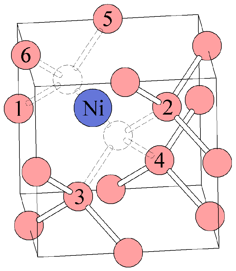
Further works on the diamond synthesis technology were focused on the synthesis in Ni, Co, and Fe solvent–catalyst systems, rather than the synthesis in an N-C system. The use of metal melts significantly reduces the diamond nucleation temperature. At the same time, the HPHT annealing procedure of diamonds was elaborated in detail. Using these new techniques, diamond crystals were synthesized in the Fe-Ni-C and Ni-C systems in Novosibirsk, Russia [19,20,21,22]. The P1 and W8 centers were observed in the EPR spectra of diamond crystals synthesized at a temperature of 1700 K and a pressure of 5.5 GPa. Then, the obtained diamond samples were annealed at different temperatures for 3–5 h. After annealing the diamond crystals at 1800 K, the W8 content decreased, and a new spectrum of the NE4 center (the abbreviation NE means nickel exhibition) with an anisotropic g-tensor (g1 = 2.0227, g2 = g3 = 2.0988) appeared. The analysis of the angular dependence of the NE4 spectrum showed that g1 corresponded to the <111> direction. Two possible models were proposed for this defect: a substitutional impurity atom with a distortion along <111>, or an impurity atom at a split-vacancy site. Large values of the g-tensor (with respect to the free electron g-factor ge = 2.0023) with large anisotropy are typical of a d ion with more than a half-filled d shell. Thus, the NE4 paramagnetic center was proposed to have a nickel atom in its structure. It was supposed that because of the large atomic radius, there was great strain around the nickel atom at the substitutional site. On annealing, the nickel atom pushed one of the nearest carbon atoms out to an interstitial position, and moved to a vacancy, forming a nickel split-vacancy defect (in some contributions this site is known as a double semi-vacancy).
Subsequent annealing of as-grown diamonds at 2100 K leads to the disappearance of the NE4 spectrum, while a new NE1 spectrum appears. The new spectrum is characterized by spin S = 1/2, the anisotropic g-tensor, and the HFS of two equivalent nitrogen atoms (see EPR parameters in Table 1). The g2 direction (14° from <110> in the (1–10) plane) corresponds to the C1–C2 direction in the split-vacancy defect (Figure 1). More information about the structure of the NE1 defect was obtained when diamond crystals were synthesized in the Ni-C system with a source material containing 5% of 13C. In the EPR spectra, the HFS of four equivalent 13C atoms was found for the NE1 center. The spectrum simulation showed that the observed ratio between the lines I(13C)/I(12C) corresponded to 4.6% 13C enrichment. The HFS tensor for 13C has an axial symmetry, with A1 parallel to the <111> direction. In accordance with the obtained g-tensor and HFS of 14N and 13C atoms, the following model was proposed for the NE1 center: the nickel atom at a split-vacancy site, with two nitrogen atoms at diametrically opposite ligand positions. The unpaired electron occupies the d(3z2-r2) orbital oriented along the N1–N2 direction.
After annealing at 2100 K, the spectrum of the NE5 center appeared along with the spectrum of the NE1 center. The new EPR spectrum can be described with S = 1/2, the anisotropic g-tensor (values larger than ge), and the HFS of two equivalent nitrogen atoms. The equivalence of nitrogen atoms in the structure of the NE5 center was established by analyzing the angular dependence of the spectrum.
An increase in the annealing temperature up to 2200 K results in the formation of two other paramagnetic centers: NE2 and NE3. For these centers, the HFS of three nitrogen atoms was distinguished. The EPR parameters of these nickel–nitrogen defects are listed in Table 1. NE2 is similar to NE1 in the g-tensor (but has lower symmetry (C1)), and the HFS tensor, for two of the nitrogen atoms. The lower symmetry of the NE2 center is associated with the additional nitrogen atom.
Finally, after annealing the diamond crystals at 2300 K, two other nitrogen–nickel paramagnetic NE8 and NE9 centers were found. The complicated EPR spectrum of NE8 was analyzed and described with the anisotropic g-factor and the HFS from four equivalent nitrogen atoms (Table 1). The 14N HFS parameters indicate that NE8 is based on a nickel split-vacancy unit with four N atoms in the plane almost normal to the g2 direction.
The second nitrogen-nickel NE9 center has the С3v symmetry, S = 1/2, and resembles the P2 paramagnetic center. The NE9 spectrum was fitted with g1 = 2.1670, g2 = g3 = 2.0910, and the HFS of three equivalent nitrogen atoms A(14N)1 = 1.22 mT, A(14N)2 = 0.76 mT, A(14N)3 = 0.64 mT. The discovered NE9 center was proposed to have the structure of three nitrogen atoms around the nickel split-vacancy unit.
3. Specific Features of the Formation of Nitrogen–Nickel Defects
As discussed previously, the transformation of the W8 center into the NE4 center is caused by strain due to a larger Ni-C bond length (~2 Å) with respect to the C-C bond length in diamond (1.54 Å). On annealing, strain around the substitutional nickel atom is relaxed by a transition of one carbon neighbor to an interstitial position; the nickel atom moves towards the created vacancy and forms a nickel split-vacancy defect. In the paper [23], it was shown that the main reason for nitrogen diffusion towards the nickel-related defects was the Coulomb interaction. The substitutional nitrogen defect donates an electron to the nickel defect. Also, there is thermal activation of nitrogen diffusion upon annealing. Based on the obtained experimental data, the formation mechanism of nitrogen–nickel defects was proposed. The evolution of the nitrogen–nickel defects consists of several stages:
- Nis− → NE4 + Ci
- NE4 + 2N → NE1 NE4 + 2N → NE5
- NE1 + N → NE2 NE5 + N → NE3
- NE5 + N → NE9 NE2 + N → NE8
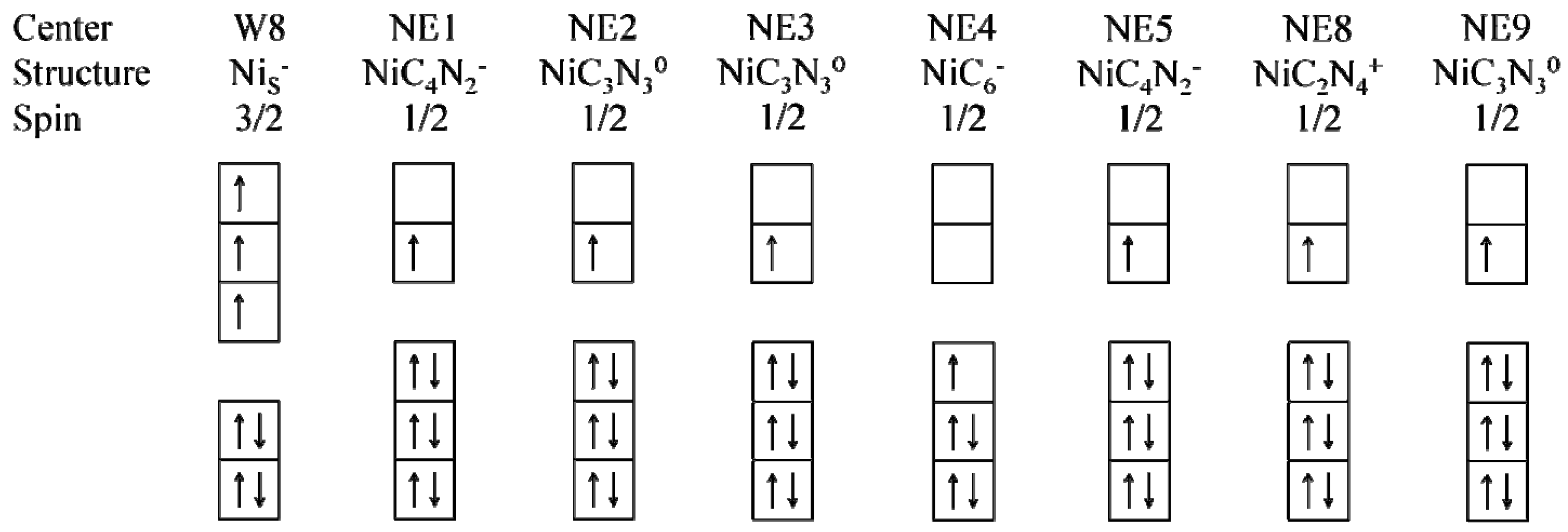
All the mentioned nitrogen–nickel defects have electron spin S = 1/2. The electronic state of nickel–nitrogen centers was described by Ludwig–Woodbury formalism (Figure 2), which was designed for transition metal ions in silicon [24]. Considering the W8 center, nickel should donate four of its 10 electrons to form bonds with four neighboring atoms. The remaining electrons, in accordance with Hund’s rule, should fill the lower orbital doublet, and then the higher orbital triplet. The W8 center is negatively charged because the substitutional nitrogen atom donates an electron. Photoillumination experiments confirmed that nitrogen centers acted as a bulk charge compensator for W8 centers [25].
For nickel split-vacancy defects, nickel should donate six of its 10 electrons to form bonds with six neighboring atoms. The remaining electrons should fill the lower orbital triplet, and then the higher orbital doublet. For the NE5 and NE1 centers, the two nitrogen atoms replace two carbon atoms, and bring two extra electrons into the system. Since the NE1 and NE5 centers have electron spin S = 1/2, these centers are supposed to be negatively charged. Substitutional nitrogen defects were proposed to be electron donors. It should be noted that the Coulomb interaction between the negatively charged NE1 and NE5 defects and positively charged substitutional nitrogen defects leads to the formation of more complex nitrogen–nickel centers.
Another scientific group synthesized diamonds in Fe-Ni-C and Ni-C systems [26,27,28,29]. The diamonds crystals have large cubic faces. After annealing the samples at 1900–2300 K for four hours, the NE1, NE2, and NE3 paramagnetic centers were observed. The other presumably nickel-containing paramagnetic centers AB1–AB5 were also detected. For the AB1–AB5 centers, the HFS of nitrogen atoms was not distinguished (Table 2).
The structure of the AB1–AB5 centers was not established. However, the authors assumed these defects to have a complex structure and to be formed as a result of aggregation of the known nickel defects (substitutional nickel atom or nickel split-vacancy defect), with some intrinsic defects (vacancies or interstitial carbon atoms). It should be noted that the formation of a <100>-split interstitial defect (R2) is energetically favorable. The R2 center has a very high mobility, and can aggregate with nickel-containing defects. Strain around the nickel atom in a tetrahedral position could be relaxed if two R2 defects were captured. It is a very tentative model of the AB3 paramagnetic center.
A defect with the same symmetry can arise if the substitutional nickel atom captures four R2 centers. This model can be proposed for the AB4 center; a smaller distortion around nickel (with respect to the AB3 center) corresponds to lower g-tensor values. The transformation of substitutional nickel defects into split-vacancy nickel defects can be a source of interstitial carbon atoms.
Since the AB1, AB2, and AB5 centers have trigonal symmetry, a possible model for these centers is the aggregation of a substitutional nickel atom with another impurity atom (for example, nitrogen) as the next neighbor. For example, the NOL1 paramagnetic center (the abbreviation NOL stands for “Novosibirsk, Oxford, London”) has trigonal symmetry about the <111> axis, and the structure of the Ni-B pair at the neighboring carbon sites [29]. Alternatively, the <111> split interstitial structure can occur near the substitutional nickel atom; in this case, the strain around nickel is relaxed. This type of defects should have a trigonal symmetry; according to the Ludwig–Woodbury formalism, the neutral charge state of such a center corresponds to spin S = 1.
The microscopic properties of nickel-related centers in diamond were investigated with density functional theory (DFT) calculations. The obtained results on the symmetry and electronic state for the Nis− center are fully consistent with the experimental data. Moreover, the calculated spin-Hamiltonian parameters (A(Ni) = 0.64 mT, A(13C)|| = 1.46 mT, A(13C)⊥ = 0.29 mT) are in good agreement with the experimental ones (A(Ni) = 0.65 mT, A(13C)|| = 1.339 mT, A(13C)⊥ = 0.340 mT) [30]. Considering the NE4 and NE8 defects with a nickel atom at a split-vacancy site, the calculated results are consistent with the experimental data in terms of spin and symmetry [31].
4. Titanium-Containing Centers in Diamond
The structure of N3 and OK1 paramagnetic centers has been discussed for 40 years. Both centers have electron spin S = 1/2, and the HFS of one nitrogen atom (Table 3) [32,33]. In the photoluminescence spectra, the OK1 paramagnetic centers correspond to the S1 system (zero-phonon lines at 503.4 nm and 510.7 nm); the N3 center has a zero-phonon line at 440.3 nm. Small HFS constants suggest a low spin density on the nitrogen atom for both centers. Initially, nitrogen-vacancy complexes were proposed as possible models for these defects [34]. These models were ruled out later, since the nitrogen-vacancy centers were shown to have other EPR parameters. Newton and Baker suggested that the OK1 and N3 paramagnetic centers contained an oxygen atom within their structure [35]. A chemical analysis of the crystals containing these centers showed the presence of an oxygen impurity. However, the oxygen HFS could not be detected in the EPR spectra, since 17O (I = 5/2, natural abundance 0.038%) is the only stable isotope with a magnetic nucleus. The finding of Novosibirsk geologists of the eclogite sample, with diamonds containing N3 and OK1 centers, stimulated new efforts in the investigation of N3 and OK1 centers [32,33]. The statistics shows that the concentration of OK1 and N3 centers inversely depends on the nitrogen concentration. This suggests that some impurity plays a role of a nitrogen getter, and is present in the structure of OK1 and N3 defects. A chemical analysis of the eclogite and its inclusion in diamond crystals shows a high titanium concentration. After that, diamond crystals were synthesized in a Fe-Ni-C system, with additional titanium as a nitrogen getter. The N3/440.3 nm center was observed in the photoluminescence spectra of the samples [36]. The analysis of the phonon structure of the N3/440.3 nm center showed that the energy of the quasi-local vibration (53 meV) corresponded to the titanium atom mass [33]. Annealing of natural diamond crystals at 2500 K for two hours showed that the N3 paramagnetic center transformed into OK1 paramagnetic centers [37].
A detailed analysis of the N3 EPR spectrum allowed the authors to assume that the N3 center had the structure of a Ti–N pair at the neighboring carbon sites (Figure 3) [32,33]. The Ti–C bond lengths (~2 Å) are considerably longer than the C–C bond in diamond (1.54 Å), which results in internal strain around the defect. On high temperature annealing, the titanium atom pushes one of the nearest carbon atoms out to the interstitial position (as well as the nickel atom). The formed OK1 center consists of a titanium atom at a split-vacancy site, with one nitrogen atom in the first coordination sphere (Figure 3).
5. Cobalt-Containing Centers in Diamond
The cobalt-containing solvent–catalyst system is also considered to be promising for diamond growth. There were no new cobalt-containing paramagnetic centers in HPHT diamond crystals synthesized in the Co–C system at 1900 K and 6 GPa. However, after annealing at 2200 K for 18 h, three new paramagnetic centers appeared: O4, NLO2, NWO1 (the abbreviation NWO stands for “Novosibirsk, Warwick, Oxford”). These centers have spin S = 1/2 and the HFS characteristic of one 59Co atom (cobalt has only one stable isotope). The spin-Hamiltonian parameters of the cobalt-containing spectra were determined (Table 4) [22].
The absence of paramagnetic cobalt-containing centers in as-grown diamonds can be explained using the Ludwig–Woodbury theory [24]. As expected, in as-grown diamond, substitutional cobalt defects formed. The cobalt atom donates four of its nine electrons to make bonds with four neighboring carbon atoms. The remaining electrons should fill the lower orbital doublet. The diamagnetic state corresponds to the positively charged state of this defect. The large atomic radius of cobalt affects distortions near the substitutional cobalt defect. On annealing at 2200 K, the produced strain is relaxed, and the cobalt atom pushes one of the nearest carbon atom to an interstitial position, and moves to the split-vacancy site. Following the well-tested Ludwig–Woodbury formalism, the cobalt split-vacancy defect would have spin S = 1/2 if the defect had the «−2» charge state. Another possibility is the presence of two nitrogen atoms in the structure of the defect, which bring two extra electrons. It allows us to imagine tree types of defects with S = 1/2, and cobalt positioned at a split-vacancy site. A careful analysis of 59Co HFS showed that only ~10% of the spin density was located on the cobalt atom. The absence of 14N HFS suggests that the spin density is localized, presumably on carbon atoms; thus, nitrogen atoms (if present) should be in the second coordination sphere.
6. Phosphorus-Containing Centers in Diamond
Doped diamond is a promising material for high-power and high-temperature semiconductor devices due to its remarkable properties, such as a wide band gap, a high breakdown field, and a high thermal conductivity. The phosphorus doping of diamond is of interest, since this type of diamond exhibits n-type conductivity, and can be used in different semiconductor applications. The first work devoted to the investigation of synthetic diamonds grown with phosphorus additions was published in 1991 [38]. The MA1 center was found with S = 1/2 and the HFS from one phosphorus atom. The phosphorus HFS constants were small, and there were no data on which atom the spin density was localized. Other attempts were made to incorporate phosphorus via ion implantation (with subsequent annealing), or during the growth. Isoya et al. measured a new EPR spectrum of NIRIM8 (NIRIM denotes the National Institute for Research in Inorganic Materials, Japan) in HPHT diamonds grown from the phosphorus–carbon system. The authors stated that the new spectrum had the HFS from one phosphorus atom and one nitrogen atom; however, no information on the parameters was provided [39]. Finally, in the late 90s, phosphorus doped (111) homoepitaxial diamond layers with n-type conductivity were obtained [40,41].
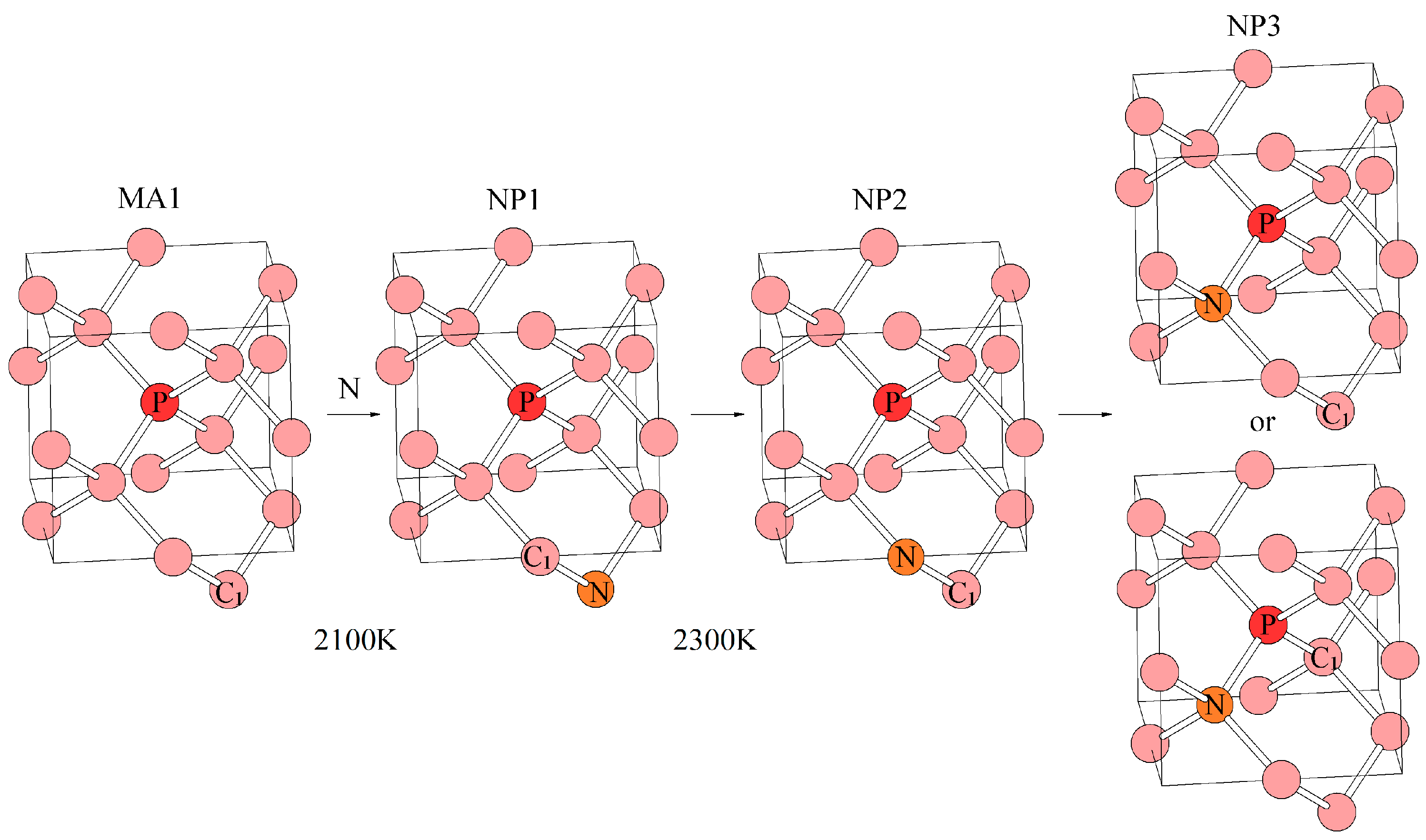
In the works of Nadolinny et al. [42,43], the HPHT diamond crystals synthesized in the P-C medium in the temperature range 1900–2100 K were studied by EPR spectroscopy. High-pressure annealing of phosphorus-containing diamonds was performed at temperatures of 2100–2600 K. For diamonds grown at 1900 K, the MA1 center was detected in the EPR spectra (see EPR parameters in Table 5). It was established that the MA1 center consisted of a substitutional phosphorus atom, and it was suggested that the spin density was localized on the C1 carbon atom that was far enough from the phosphorus atom. The s/p hybridization parameter for the C1 carbon atom was found to be similar to that of the undistorted lattice. Annealing at a higher temperature (the high-pressure annealing was performed at temperatures of 2100 and 2300 K for two hours) leads to the aggregation of P1 centers (substitutional nitrogen defects) with MA1 centers (substitutional phosphorus defects), and different phosphorus–nitrogen pairs form (Figure 4). On the first step, the nitrogen–phosphorus pairs separated by two carbon atoms are formed (NIRIM8 or NP1 center). The abbreviation NP corresponds to nitrogen–phosphorus defects. With an increase in the annealing temperature, the nitrogen and phosphorus atoms move closer, and form nitrogen-phosphorus pairs separated by one carbon atom (NP2 centers) and close nitrogen–phosphorus pairs (NP3 centers). On the one hand, this behavior can be explained by the Coulomb interaction between the phosphorus and nitrogen atoms. In the theoretical work of Anderson et al. [44], it was shown that substitutional nitrogen could act as an electron acceptor for substitutional phosphorus. In addition, the possibility for nitrogen and phosphorus to form a close pair was discussed in this paper [44]. On the other hand, the increased annealing temperature allows the nitrogen atom diffusing towards the phosphorus atom to overcome the energy barrier. The energy barrier arises as a result of strain around the phosphorus atom having a large atomic radius.
It is interesting to note that the NP1–NP3 centers have electron spin S = 1/2, which means that these centers must be positively charged. The substitutional nitrogen defects can play the role of the acceptor for these nitrogen–phosphorus defects. In the work of Jones et al. [45], the energy state of negatively-charged substitutional nitrogen was calculated, and shown to be close to the energy state of neutral substitutional nitrogen.
Annealing of diamond crystals at 2600 K for 10 minutes leads to the disappearance of the NP1–NP3 centers, and the detection of new paramagnetic centers (NP4, NP5, and NP6) (Table 5) [46]. The NP4, NP5, and NP6 centers have the HFS of only one phosphorus atom. It is noteworthy that the EPR spectrum of the NP5 and NP6 centers appears after X-ray irradiation of the diamond crystals. Annealing at 800 K results in the reversible disappearance of the NP5 and NP6 spectra.
It was supposed that when a large phosphorus atom occupied the substitutional site, it generated high strain around a defect. On annealing at 2600 K, the NP1–NP3 centers transform into the NP4–NP6 centers. The analysis of the 31P HFS for the NP4–NP6 centers revealed a low spin density on the phosphorus atom. The obtained result is consistent with the data obtained in the theoretical work of Jones et al. [47]; it was shown that there was a low spin density on the P atom for the phosphorus split-vacancy defect. One can assume that the NP4–NP6 centers differ in distances between the nitrogen atom and the split-vacancy fragment. For the NP4 center consisting of a phosphorus split-vacancy defect, the unpaired electron is localized on a dangling bond of the carbon atom. In the case of NP5 and NP6 centers, the presence of a nitrogen atom in the second or third coordination spheres results in electron transfer from the nitrogen atom to the dangling bond of the carbon atom, making these centers diamagnetic. However, an electron can be trapped as a result of X-ray irradiation, which makes these two centers paramagnetic.
Two new phosphorus paramagnetic centers were detected in HPHT diamonds synthesized in the phosphorus–carbon system with aluminum introduced into the system as a getter (Table 5) [48]. Also, a decrease in the temperature of the spectral measurement leads to the appearance of a new EPR spectrum in the form of a Dyson line associated with conductivity electrons. Thus, it can be concluded that nitrogen prevents the formation of n-type conductivity in diamond.
It should be noted that the tetrahedral environment of a phosphorus atom transforms into an octahedral environment at a very high annealing temperature. The high formation temperature of the NP4–NP6 defects can be explained by the fact that impurity nitrogen can slightly relax strain around the substitutional phosphorus defect. The same tendency can be noted for the titanium-containing centers; the OK1 center (in which a titanium atom is located at a split-vacancy site) is formed at a temperature above 2300 K.
7. Silicon-Vacancy Defect in Diamond
During the last 15 years, optically active centers in diamond have been extensively studied. Nitrogen-vacancy, silicon-vacancy, and germanium-vacancy centers are the most known color centers. These defects are thought to be promising as single photon emitters in different quantum applications. The NV0 and NV− centers have zero-phonon lines at 575 and 637 nm. The NV− center is paramagnetic, and has the EPR spectrum fitted with S = 1, g = 2.0028, D = 103 mT, A(14N) = 0.08 mT, А(13С)|| = 7.31 mT, А(13С)⊥ = 4.40 mT [49].
The NV− center shows a significant phonon sideband in photoluminescence spectra, and this defect has a long excited state lifetime (~10 ns [50]). Thus, other optically active centers were sought. In 1980, Vavilov et al. detected a 737 nm optical system (attributed later to the SiV− center) for diamond films grown on a silicon substrate [51]. Silicon ion implantation resulted in the appearance of the 737 nm system [52]. In subsequent papers [53,54], it was shown that electron irradiation of silicon-containing diamonds followed by annealing (at a temperature of 1000 K) resulted in an increase in the 737 nm system. At a temperature of 1000 K, the vacancy becomes mobile in diamond. It was concluded that the center responsible for the 737 nm luminescence was a vacancy trapped in silicon. The hypothesis about the negative charge state of the defect was suggested by Collins et al. [52]. They showed that the 737 nm system was more intense in silicon-implanted diamonds that had a high concentration of substitutional nitrogen, which usually acted as an electron donor.
Different possible charges and spin states of the silicon-vacancy defect made it interesting to study silicon doped diamonds by EPR. The neutral silicon-vacancy defect was shown to be paramagnetic. The corresponding spectrum (KUL1) has an axial symmetry around <111> and was fitted with the following spin-Hamiltonian parameters: S = 1, g|| = 2.0040, g⊥ = 2.0035, D = 35.8 mT, Е = 0 [55,56,57]. In a later work [58], the HFS of one 29Si atom (А(29Si)|| = 2.73 mT, А(29Si)⊥ = 2.82 mT) and the HFS of six equivalent 13C atoms (А(13C)|| = 2.36 mT, А(13C)⊥ = 1.08 mT) were detected. It was shown that approximately 75% of the spin density was localized on these six carbon atoms. Based on the obtained data, this paramagnetic center was concluded to be a neutral silicon split-vacancy defect. A paramagnetic SiV0 center was also studied at the DFT level; the structure and electronic properties of the defect were analyzed [59]. The calculated EPR parameters (А(29Si)|| = 2.79 mT, А(29Si)⊥ = 2.93 mT, А(13C)|| = 1.82 mT, А(13C)⊥ = 0.43 mT) are in good agreement with those determined experimentally.
The negatively charged silicon-vacancy center (responsible for the 737 nm optical system) was also expected to be paramagnetic. It was reported [56,57] that the KUL8 spectrum (S = 1/2, g1 = 2.00368, g2 = 2.00336, g3 = 2.00336) corresponded to the SiV− center. However, the KUL8 spectrum was not detected in a series of experiments on charge transfer between SiV− and SiV0, which was induced by UV photoexcitation or heating [60].
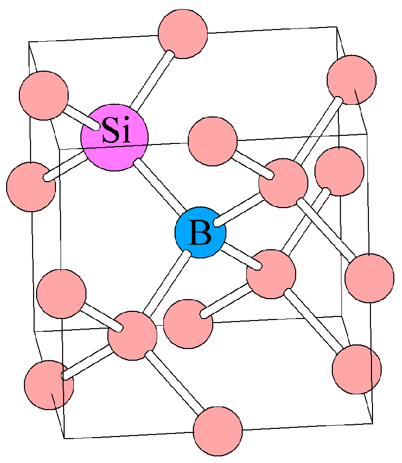
Along with the peak at 737 nm, a weak peak at 720 nm is often observed in the photoluminescence spectra of diamond crystals synthesized in the silicon-containing medium. It was supposed that the peak at 720 nm could be attributed to an unknown silicon-related center. Since boron is usually present in diamond as a trace impurity, the possibility of the formation of a silicon-boron defect was considered. The HPHT diamond crystals were synthesized in the Mg–C system, with the addition of various amounts of Si and B [61]. In the photoluminescence spectra of the samples, the intense 720 nm system was detected. At the same time, a new EPR spectrum fitted with S = 1/2 and an anisotropic g-factor was observed: g1 = 2.0033, g2 = 2.0004, g3 = 2.0024. The g3 value corresponds to (01-1). The angle between the principal direction of g1 and (011) is 50°. Thus, the principal direction of g2 is close to the (1-1-1) axis. It can be noted that the g-tensor values and principle axes are similar to those of the N3 paramagnetic center, which consisted of titanium and nitrogen atoms at the adjacent carbon sites. Thus, the 720 nm system was tentatively ascribed to the center containing silicon and boron atoms at the adjacent carbon sites (Figure 5). Experiments on HPHT annealing of the diamond crystals showed that the new center was stable up to 2200 K.
8. Germanium-Vacancy Defect in Diamond
The EPR study of diamond crystals synthesized in the Mg-Ge-C system revealed the spectrum of an unknown paramagnetic center. The analysis of the angular dependence of the EPR spectrum showed that it was characterized by an axial symmetry around <111> and had the following spin-Hamiltonian parameters: S = 1, g|| = 2.0025, g⊥ = 2.0027, D = 80.3 mT, E = 0 [61]. As shown previously, several models can be proposed for a defect with a trigonal symmetry around <111> For the newly observed center, the germanium split-vacancy model is more preferred because of the large atomic radius of germanium. The new paramagnetic center has the same symmetry and spin state as the SiV0 center [58]; thus, the new spectrum was ascribed to the neutral germanium split-vacancy defect.
To confirm the assumption that the new paramagnetic center contains a germanium atom in the structure, additional growth experiments were performed using germanium enriched with the 73Ge isotope (I = 9/2). For the GeV0 paramagnetic center, the HFS of one 73Ge atom was detected with an almost isotropic constant A(73Ge) ≈ 1.64 mT. The hyperfine interaction was almost isotropic for 73Ge as for the 29Si atom in the structure of the SiV0 center.
The new center has a large zero-field splitting parameter D, which was suggested to be a result of the spin–orbit interaction. As is known, the zero-field splitting has two contributions: a term arising from the spin–spin dipole–dipole interaction, and a term arising from the spin–orbit coupling. Indeed, Ge has a significantly larger spin–orbit coupling constant than Si (λ(Ge) = 940 cm−1, λ(Si) = 149 cm−1 [62]), which may result in a larger D value.
The structure and electronic properties of the GeV0 defect were analyzed at the DFT level [63]. The EPR parameters (g-tensor, hyperfine interaction constants, and zero-field splitting (ZFS) parameters) were calculated. It was shown that the spin–orbit coupling interaction actually gave a dominant contribution to the total D parameter. In Table 6, the calculated and experimentally determined spin-Hamiltonian parameters are presented with good agreement.
9. Conclusions
The obtained results on the HPHT synthesis have shown that atoms with large atomic radii can be introduced into the diamond crystal lattice. Nickel-, cobalt-, titanium-, phosphorus-, germanium-, and silicon-related point defects were detected in diamond. As a rule, in the diamond crystals synthesized at relatively low temperatures, large impurity atoms occupy substitutional positions. In this case, the bond length between the impurity and carbon atoms is sufficiently longer than the carbon–carbon bond length, which causes distortions and strain around the defect. Among the defects with a large impurity atom at a substitutional position, only substitutional phosphorus (in the neutral charge state) and nickel (in the negative charged state) defects were observed. This made the investigation of defects with heavy impurity atoms rather complicated. On HPHT annealing, the thermal vibration results in relaxing the structure; then, the impurity atom pushes one of the nearest atoms out to the interstitial position. The split-vacancy structure with an impurity atom is formed; this defect has the D3d symmetry. The tetrahedral environment of the impurity atom usually transforms into the octahedral one at a temperature enabling the thermal diffusion of nitrogen. The Coulomb interaction can be a driving force for the nitrogen diffusion towards another impurity atom.
For the defects with two impurity atoms at the adjacent carbon sites (Ti-N, Ni-B, P-N and Si-B), the tetrahedral environment of a large impurity atom transforms into the octahedral environment at higher temperatures. This effect can be explained by partial relaxation of the structure around the Ti, Ni, P or Si atoms.
It should be emphasized that the aggregation of phosphorus atoms with nitrogen atoms is also caused by the Coulomb interaction. The experiment on HPHT annealing of diamonds synthesized in the P-C system confirmed the previous theoretical prediction that the substitutional nitrogen defect could act as an electron donor for the substitutional phosphorus defect. Thus, the presence of a nitrogen impurity prevents the formation of n-type conductivity in diamonds synthesized with the addition of phosphorus.
It was established that the electronic state of the transition metal centers was well described by the Ludwig–Woodbury formalism. In the case of the tetrahedral environment of a transition metal atom, it donates four electrons to form bonds with the neighboring atoms. The remaining electrons fill the lower orbital doublet, and then the higher orbital triplet. In the case of the octahedral environment of a transition metal atom, it donates six electrons to form bonds with carbon atoms. The remaining electrons fill the lower orbital triplet, and then the higher orbital doublet.
Acknowledgments
This work was supported by the Russian Science Foundation under Grant No. 14-27-00054.
Author Contributions
Vladimir Nadolinny, Andrey Komarovskikh and Yuri Palyanov contributed equally to the writing of the manuscript.
Conflicts of Interest
The authors declare no conflict of interest. The founding sponsors had no role in the design of the study; in the collection, analyses, or interpretation of data; in the writing of the manuscript, and in the decision to publish the results.
References
- Bragg, W.H.; Bragg, W.L. The Structure of the Diamond. Nature 1913, 2283, 557. [Google Scholar] [CrossRef]
- Robertson, R.; Fox, J.J.; Martin, A.E. Two Types of Diamond. Philos. Trans. R. Soc. Lond. A 1934, 232, 463–535. [Google Scholar] [CrossRef]
- Kaiser, W.; Bond, W.L. Nitrogen, A Major Impurity in Common Type I Diamond. Phys. Rev. 1959, 115, 857–863. [Google Scholar] [CrossRef]
- Dyer, H.B.; Raal, F.A.; Du Preez, L.; Loubser, J.H.N. Optical absorption features associated with paramagnetic nitrogen in diamond. Philos. Mag. 1965, 11, 763–774. [Google Scholar] [CrossRef]
- Smith, W.V.; Sorokin, P.P.; Gelles, I.L.; Lasher, G.J. Electron-Spin Resonance of Nitrogen Donors in Diamond. Phys. Rev. 1959, 115, 1546–1552. [Google Scholar] [CrossRef]
- Woods, G.S.; van Wyk, J.A.; Collins, A.T. The nitrogen content of type Ib synthetic diamond. Philos. Mag. Part B 1990, 62, 589–595. [Google Scholar] [CrossRef]
- Collins, A.T.; Stanley, M.; Woods, G.S. Nitrogen isotope effects in synthetic diamonds. J. Phys. D Appl. Phys. 1987, 20, 969–974. [Google Scholar] [CrossRef]
- Lawson, S.C.; Fisher, D.; Huntz, D.C.; Newton, M.E. On the existence of positively charged single-substitutional nitrogen in diamond. J. Phys. Condens. Matter 1998, 10, 6171–6180. [Google Scholar] [CrossRef]
- Boyd, S.R.; Kiflawi, I.; Woods, G.S. The relationship between infrared absorption and the A defect concentration in diamond. Philos. Mag. Part B 1994, 69, 1149–1153. [Google Scholar] [CrossRef]
- Collins, A.T.; Williams, A.W.S. The nature of the acceptor centre in semiconducting diamond. J. Phys. C Solid State Phys. 1971, 4, 1789–1800. [Google Scholar] [CrossRef]
- Evans, T.; Qi, Z. The kinetics of aggregation of nitrogen atoms in diamond. Proc. R. Soc. Lond. A 1982, 381, 159–178. [Google Scholar] [CrossRef]
- Mainwood, A. Nitrogen and nitrogen-vacancy complexes and their formation in diamond. Phys. Rev. B 1994, 49, 7934–7940. [Google Scholar] [CrossRef]
- Jones, R.; Briddon, P.R.; Öberg, S. First-principles theory of nitrogen aggregates in diamond. Philos. Mag. Lett. 1992, 66, 67–74. [Google Scholar] [CrossRef]
- Shcherbakova, M.Y.; Nadolinny, V.A.; Sobolev, E.V. The N3 center in natural diamonds, from ESR data. J. Struct. Chem. 1978, 19, 261–269. [Google Scholar] [CrossRef]
- Van Wyk, J.A. Carbon-12 hyperfine interaction of the unique carbon of the P2 (ESR) or N3 (optical) centre in diamond. J. Phys. C Solid State Phys. 1982, 15, L981–L983. [Google Scholar] [CrossRef]
- Woods, G.S.; Collins, A.T. Infrared absorption spectra of hydrogen complexes in type I diamonds. J. Phys. Chem. Solids 1983, 44, 471–475. [Google Scholar] [CrossRef]
- Samoilovich, M.I.; Bezrukov, G.N.; Butuzov, V.P. Electron paramagnetic resonance of nickel in synthetic diamond. JETP Lett. 1971, 14, 379–381. [Google Scholar]
- Isoya, J.; Kanda, H.; Norris, J.R.; Tang, J.; Bowman, M.K. Fourier-transform and continuous-wave EPR studies of nickel in synthetic diamond: Site and spin multiplicity. Phys. Rev. B 1990, 41, 3905–3913. [Google Scholar] [CrossRef]
- Nadolinny, V.A.; Yelisseyev, A.P. New paramagnetic centres containing nickel ions in diamond. Diam. Relat. Mater. 1993, 3, 17–21. [Google Scholar] [CrossRef]
- Nadolinny, V.A.; Yelisseyev, A.P. Structure and creation conditions of complex nitrogen-nickel defects in synthetic diamonds. Diam. Relat. Mater. 1994, 3, 1196–1200. [Google Scholar] [CrossRef]
- Nadolinny, V.A.; Yelisseyev, A.P.; Baker, J.M. A study of 13C hyperfine structure in the EPR of nickel-nitrogen-containing centres in diamond and correlation with their optical properties. J. Phys. Condens. Matter 1999, 11, 7357–7376. [Google Scholar] [CrossRef]
- Nadolinny, V.A.; Baker, J.M.; Yuryeva, O.P. EPR Study of the Peculiarities of Incorporating Transition Metal Ions into the Diamond Structure. Appl. Magn. Reson. 2005, 28, 365–381. [Google Scholar] [CrossRef]
- Nadolinny, V.A.; Yelisseyev, A.P.; Baker, J.M.; Twitchen, D.J.; Newton, M.E.; Feigelson, B.N.; Yuryeva, O.P. Mechanisms of nitrogen aggregation in nickel- and cobalt-containing synthetic diamonds. Diam. Relat. Mater. 2000, 9, 883–886. [Google Scholar] [CrossRef]
- Ludwig, G.W.; Woodbury, H.H. Electron Spin Resonance in Semiconductors. Solid State Phys. 1962, 13, 223–304. [Google Scholar] [CrossRef]
- Nadolinny, V.; Yelisseyev, A.; Yurjeva, O.; Hofstaetter, A.; Meyer, B.; Feigelson, B. Relationship between electronic states of nickel-containing centres and donor nitrogen in synthetic and natural diamonds. Diam. Relat. Mater. 1998, 7, 1558–1561. [Google Scholar] [CrossRef]
- Pereira, R.N.; Neves, A.J.; Gehlhoff, W.; Sobolev, N.A.; Rino, L.; Kanda, H. Annealing study of the formation of nickel-related paramagnetic defects in diamond. Diam. Relat. Mater. 2002, 11, 623–626. [Google Scholar] [CrossRef]
- Neves, A.J.; Pereira, R.; Sobolev, N.A.; Nazare, M.H.; Gehlhoff, W.; Naser, A.; Kanda, H. New paramagnetic defects in synthetic diamonds grown using nickel catalyst. Physica B 1999, 273–274, 651–654. [Google Scholar] [CrossRef]
- Neves, A.J.; Pereira, R.; Sobolev, N.A.; Nazare, M.H.; Gehlhoff, W.; Naser, A.; Kanda, H. New paramagnetic centers in annealed high-pressure synthetic diamond. Diam. Relat. Mater. 2000, 9, 1057–1060. [Google Scholar] [CrossRef]
- Rakhmanova, M.I.; Nadolinny, V.A.; Yuryeva, O.P. Impurity Centers in Synthetic and Natural Diamonds with a System of Electron-Vibronic Lines at 418 nm in Luminescence Spectra. Phys. Solid State 2013, 55, 127–130. [Google Scholar] [CrossRef]
- Larico, R.; Assali, L.V.C.; Machado, W.V.M. Isolated nickel impurities in diamond: A microscopic model for the electrically active centers. Appl. Phys. Lett. 2004, 84, 720–722. [Google Scholar] [CrossRef]
- Larico, R.; Justo, J.F.; Machado, W.V.M.; Assali, L.V.C. Electronic properties and hyperfine fields of nickel-related complexes in diamond. Phys. Rev. B 2009, 79, 115202. [Google Scholar] [CrossRef]
- Nadolinny, V.A.; Yuryeva, O.P.; Shatsky, V.S.; Stepanov, A.S.; Golushko, V.V.; Rakhmanova, M.I.; Kupriyanov, I.N.; Kalinin, A.A.; Palyanov, Y.N.; Zedgenizov, D. New Data on the Nature of the EPR OK1 and N3 Centers in Diamond. Appl. Magn. Reson. 2009, 36, 97–108. [Google Scholar] [CrossRef]
- Nadolinny, V.A.; Yuryeva, O.P.; Rakhmanova, M.I.; Shatsky, V.S.; Palyanov, Y.N.; Kupriyanov, I.N.; Zedgenizov, D.A.; Ragozin, A.L. Distribution of OK1, N3, and NU1 defects in diamonds of different habits. Eur. J. Mineral. 2012, 24, 645–650. [Google Scholar] [CrossRef]
- Scherbakova, M.Y.; Sobolev, E.V.; Nadolinny, V.A. Electron paramagnetic resonance of low-symmetry impurity centers in diamond. Dokl. Acad. Nauk SSSR 1972, 204, 851–854. (In Russian) [Google Scholar]
- Newton, M.E.; Baker, J.M. 14N ENDOR of the OK1 centre in natural type Ib diamond. J. Phys. Condens. Matter 1989, 1, 10549–10561. [Google Scholar] [CrossRef]
- Nadolinny, V.; Yuryeva, O.; Chepurov, A.; Shatsky, V. Titanium Ions in the Diamond Structure: Model and Experimental Evidence. Appl. Magn. Reson. 2009, 36, 109–113. [Google Scholar] [CrossRef]
- Nadolinny, V.; Palyanov, Y.; Yuryeva, O.; Zedgenizov, D.; Rakhmanova, M.; Kalinin, A.; Komarovskikh, A. The influence of HTHP treatment on the OK1 and N3 centers in natural diamonds. Phys. Status Solidi A 2015, 212, 2474–2479. [Google Scholar] [CrossRef]
- Samsonenko, N.D.; Tokii, V.V.; Gorban, S.V. Electron paramagnetic resonance of phosphorus in diamond. Fiz. Tver. Tela 1991, 33, 2496–2498. (In Russian) [Google Scholar]
- Isoya, J.; Kanda, H.; Akaishi, M.; Morita, Y.; Ohshima, T. ESR studies of incorporation of phosphorus into high-pressure synthetic diamond. Diam. Relat. Mater. 1997, 6, 356–360. [Google Scholar] [CrossRef]
- Koizumi, S.; Kamo, M.; Sato, Y.; Ozaki, H.; Inuzuka, T. Growth and characterization of phosphorous doped {111} homoepitaxial diamond thin films. Appl. Phys. Lett. 1997, 71, 1065–1067. [Google Scholar] [CrossRef]
- Hasegawa, M.; Teraji, T.; Koizumi, S. Lattice location of phosphorus in n-type homoepitaxial diamond films grown by chemical-vapor deposition. Appl. Phys. Lett. 2001, 79, 3068–3070. [Google Scholar] [CrossRef]
- Nadolinny, V.A.; Palyanov, Y.N.; Kupriyanov, I.N.; Newton, M.J.; Kryukov, E.; Sokol, A.G. A new EPR data on the MA1 and NIRIM8 (NP1) phosphorus-related centers in synthetic 1b diamonds. Appl. Magn. Reson. 2012, 42, 179–186. [Google Scholar] [CrossRef]
- Nadolinny, V.A.; Pal’yanov, Y.N.; Kalinin, A.A.; Kupriyanov, I.N.; Veber, S.L.; Newton, M.J. Transformation of As-Grown Phosphorus-Related Centers in HPHT Treated Synthetic Diamonds. Appl. Magn. Reson. 2011, 41, 371–382. [Google Scholar] [CrossRef]
- Anderson, A.B.; Kostadinov, L.N. P and N compensation in diamond molecular orbital theory. J. Appl. Phys. 1997, 81, 264–267. [Google Scholar] [CrossRef]
- Jones, R.; Goss, J.P.; Briddon, P.R. Acceptor level of nitrogen in diamond and the 270-nm absorption band. Phys. Rev. B 2009, 80, 033205. [Google Scholar] [CrossRef]
- Nadolinny, V.; Komarovskikh, A.; Pal’yanov, Y.; Kupriyanov, I. EPR of new phosphorus-containing centers in synthetic diamonds. Phys. Status Solidi A 2013, 210, 2078–2082. [Google Scholar] [CrossRef]
- Jones, R.; Lowther, J.E.; Goss, J. Limitations to n-type doping in diamond: The phosphorus-vacancy complex. Appl. Phys. Lett. 1996, 69, 2489–2491. [Google Scholar] [CrossRef]
- Nadolinny, V.; Komarovskikh, A.; Palyanov, Y.; Sokol, A. EPR of synthetic diamonds heavily doped with phosphorus. Phys. Status Solidi A 2015, 212, 2568–2571. [Google Scholar] [CrossRef]
- Loubser, J.H.N.; van Wyk, J.A. Electron spin resonance in the study of diamond. Rep. Prog. Phys. 1978, 41, 1201–1248. [Google Scholar] [CrossRef]
- Collins, A.T.; Thomaz, M.F.; Jorge, M.I.B. Luminescence decay time of the 1.945 eV centre in type Ib diamond. J. Phys. C Solid State Phys. 1983, 16, 2177–2181. [Google Scholar] [CrossRef]
- Vavilov, V.S.; Gippius, A.A.; Zaitsev, A.M.; Deryagin, B.V.; Spitsyn, B.V.; Aleksenko, A.E. Investigation of the cathodoluminescence of epitaxial diamond films. Fiz. Tekh. Polyprovodn. 1980, 14, 1811–1813. (In Russian) [Google Scholar]
- Collins, A.T.; Kamo, M.; Sato, Y. A spectroscopic study of optical centers in diamond grown by microwave-assisted chemical vapor deposition. J. Mater. Res. 1990, 5, 2507–2514. [Google Scholar] [CrossRef]
- Clark, C.D.; Dickerson, C.B. The 1.681 eV centre in polycrystalline diamond. Surf. Coat. Technol. 1991, 47, 336–343. [Google Scholar] [CrossRef]
- Collins, A.T.; Allers, L.; Wort, C.J.H.; Scarsbrook, G.A. The annealing of radiation damage in De Beers colourless CVD diamond. Diam. Relat. Mater. 1994, 3, 932–935. [Google Scholar] [CrossRef]
- Iakoubovskii, K.; Stesmans, A. Characterization of Defects in as-Grown CVD Diamond Films and HPHT Diamond Powders by Electron Paramagnetic Resonance. Phys. Status Solidi A 2001, 186, 199–206. [Google Scholar] [CrossRef]
- Iakoubovskii, K.; Stesmans, A. Characterization of hydrogen and silicon-related defects in CVD diamond by electron spin resonance. Phys. Rev. B 2002, 66, 195207. [Google Scholar] [CrossRef]
- Iakoubovskii, K.; Stesmans, A.; Suzuki, K.; Kuwabara, J.; Sawabe, A. Characterization of defects in monocrystalline CVD diamond films by electron spin resonance. Diam. Relat. Mater. 2003, 12, 511–515. [Google Scholar] [CrossRef]
- Edmonds, A.M.; Newton, M.E.; Martineau, P.M.; Twitchen, D.J.; Williams, S.D. Electron paramagnetic resonance studies of silicon-related defects in diamond. Phys. Rev. B 2008, 77, 245205. [Google Scholar] [CrossRef]
- Goss, J.P.; Briddon, P.R.; Shaw, M.J. Density functional simulations of silicon-containing point defects in diamond. Phys. Rev. B 2007, 76, 075204. [Google Scholar] [CrossRef]
- D’Haenens-Johansson, U.F.S.; Edmonds, A.M.; Green, B.L.; Newton, M.E.; Davies, G.; Martineau, P.M.; Khan, R.U.A.; Twitchen, D.J. Optical properties of the neutral silicon split-vacancy center in diamond. Phys. Rev. B 2011, 84, 245208. [Google Scholar] [CrossRef]
- Nadolinny, V.; Komarovskikh, A.; Palyanov, Y.; Kupriyanov, I.; Borzdov, Y.; Rakhmanova, M.; Yuryeva, O.; Veber, S. EPR study of Si- and Ge-related defects in HPHT diamonds synthesized from Mg-based solvent-catalysts. Phys. Status Solidi A 2016, 213, 2623–2628. [Google Scholar] [CrossRef]
- Pzhezhetskii, S.Y. EPR Svobodnykh Radikalov v Radiatsionnoi Khimii, 1st ed.; Khimiya: Moscow, Russia, 1972; p. 30. (In Russian) [Google Scholar]
- Komarovskikh, A.; Dmitriev, A.; Nadolinny, V.; Palyanov, Y. A DFT calculation of EPR parameters of a germanium-vacancy defect in diamond. Diam. Relat. Mater. 2017, 76, 86–89. [Google Scholar] [CrossRef]
- Wang, C.; Kurtsiefer, C.; Weinfurter, H.; Burchard, B. Single photon emission from SiV centres in diamond produced by ion implantation. J. Phys. B 2006, 39, 37–41. [Google Scholar] [CrossRef]
- Iwasaki, T.; Ishibashi, F.; Miyamoto, Y.; Doi, Y.; Kobayashi, S.; Miyazaki, T.; Tahara, K.; Jahnke, K.D.; Rogers, L.J.; Naydenov, B.; et al. Germanium-Vacancy Single Color Centers in Diamond. Sci. Rep. 2015, 5, 12882. [Google Scholar] [CrossRef] [PubMed]
Figure 1.
The diamond unit cell with a nickel atom at a split-vacancy site.

Figure 2.
Electronic state of nickel-containing centers in diamond.

Figure 3.
(a) Proposed model for the N3 center. (b) Proposed model for the OK1 center.
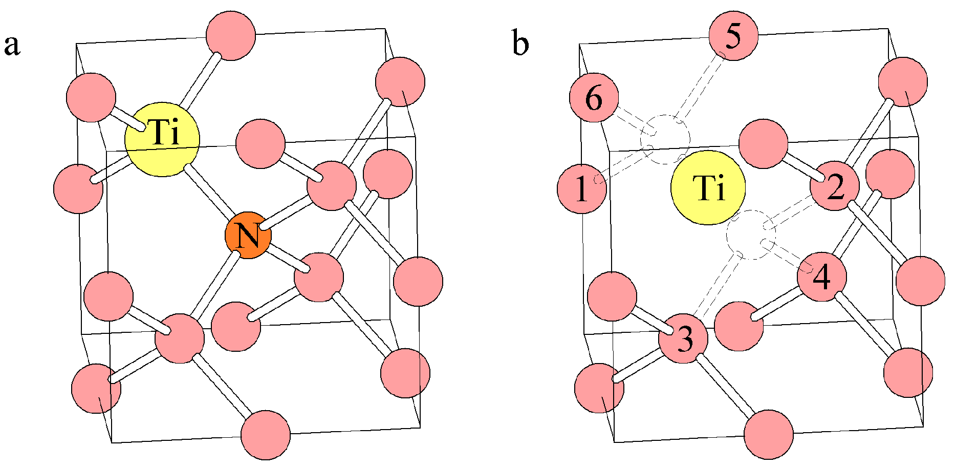
Figure 4.
Supposed structures of MA1, NP1 (NIRIM8), NP2, and NP3 centers in synthetic microdiamonds grown in the C–P system.
Figure 4.
Supposed structures of MA1, NP1 (NIRIM8), NP2, and NP3 centers in synthetic microdiamonds grown in the C–P system.

Figure 5.
Proposed model for the Si-B center.

Table 1.
Parameters of the spin Hamiltonian for different nickel-containing centers with S = 1/2 in diamond [19,20,21,22]. The directions are for a C2h symmetry site with (1–10) as its plane of reflection symmetry. g1 corresponds to (1–10), and α is the angle between g2 and <110>. NE2 has the C1 symmetry, and g1 is 20° from (1–10). β is the angle between A1 and <111>, A3 corresponds to (1–10). γ is the angle between A1 and (1-1-1) or (-11-1) that rotates towards (1–10), A2 is perpendicular to the (110) plane. For the NE2 center, the hyperfine structure (HFS) from 13C was determined unambiguously only for the (100) orientation of the crystal with respect to the magnetic field.
| Center | g-Value | Constant A (mT) | |||||
|---|---|---|---|---|---|---|---|
| Atom Number | |||||||
| 1 | 2 | 3 | 4 | 5 | 6 | ||
| NE1 | g1 = 2.1282 | AN1 = 2.09 | AN1 = 2.09 | AC1 = 1.74 | AC1 = 1.74 | AC1 = 1.74 | AC1 = 1.74 |
| g2 = 2.0070 | AN2 = 1.43 | AN2 = 1.43 | AC2 = 1.12 | AC2 = 1.12 | AC2 = 1.12 | AC2 = 1.12 | |
| g3 = 2.0908 | AN3 = 1.45 | AN3 = 1.45 | AC3 = 1.12 | AC3 = 1.12 | AC3 = 1.12 | AC3 = 1.12 | |
| α = 14° | β = 5° | β = 5° | γ = 0° | γ = 0° | γ = 0° | γ = 0° | |
| NE2 | g1 = 2.1301 | AN1 = 2.10 | AN1 = 1.87 | AN1 = 0.18 | AC = 1.12 | AC = 1.12 | AC = 1.12 |
| g2 = 2.0100 | AN2 = 1.42 | AN2 = 1.18 | AN2 = 0.35 | ||||
| g3 = 2.0931 | AN3 = 1.41 | AN3 = 1.25 | AN3 = 0.25 | ||||
| α = 14° | β = 3° | β = 0° | β = 0° | ||||
| NE3 | g1 = 2.0729 | AN1 = 1.60 | AN1 = 0.66 | AN1 = 0.66 | |||
| g2 = 2.0100 | AN2 = 1.24 | AN2 = 0.50 | AN2 = 0.50 | ||||
| g3 = 2.0476 | AN3 = 1.15 | AN3 = 0.50 | AN3 = 0.50 | ||||
| α = 14° | β = 4° | γ = 0° | γ = 0° | ||||
| NE5 | g1 = 2.0329 | AN1 = 1.22 | AN1 = 1.22 | AC1 = 4.14 | AC1 = 4.14 | ||
| g2 = 2.0898 | AN2 = 0.98 | AN2 = 0.98 | AC2 = 2.58 | AC2 = 2.58 | |||
| g3 = 2.0476 | AN3 = 0.89 | AN3 = 0.89 | AC3 = 2.49 | AC3 = 2.49 | |||
| α = 27.5° | γ = 3.8° | γ = 3.8° | γ = 0° | γ = 0° | |||
| NE8 | g1 = 2.0439 | AN1 = 1.14 | AN1 = 1.14 | AN1 = 1.14 | AN1 = 1.14 | ||
| g2 = 2.1722 | AN2 = 0.78 | AN2 = 0.78 | AN2 = 0.78 | AN2 = 0.78 | |||
| g3 = 2.0476 | AN3 = 0.75 | AN3 = 0.75 | AN3 = 0.75 | AN3 = 0.75 | |||
| α = 27.5° | γ = 9.8° | γ = 9.8° | γ = 9.8° | γ = 9.8° | |||
| Center | Spin | g-Value | Zero-Field Splitting (T) |
|---|---|---|---|
| AB1 | S = 1/2 | g|| = 2.0024||(111), g⊥ = 2.0920⊥(111) | - |
| AB2 | S = 1/2 | g|| = 2.0072||(111), g⊥ = 2.0672⊥(111) | - |
| AB3 | S = 1/2 | g1 = 2.1105||(100), g2 = 2.0663||(011), g3 = 2.0181||(0–11) | - |
| AB4 | S = 1/2 | g1 = 2.0220||(100), g2 = 2.0094||(011), g3 = 2.0084||(0–11) | - |
| AB5 | S = 1 | g|| = 2.037||(111), g⊥ = 2.022⊥(111) | D = ±1.132 |
| NOL1 (NIRIM5) | S = 1 | g|| = 2.0235||(111), g⊥ = 2.002⊥(111) | D = −6.10 |
Table 3.
Electron paramagnetic resonance (EPR) parameters for titanium-containing centers with S = 1/2 in diamond. g1(A1) corresponds to (1–10), α is the angle between g2(A2) and (110). γ is the angle between A1 and (1-1-1) or (-11-1) that rotates towards (1–10), A2 is perpendicular to the (110) plane [32,33].
| Center | g-Value | A(14N) (mT) | A(13C) (mT) | A(47Ti, 49Ti) (mT) |
|---|---|---|---|---|
| N3 | g1 = 2.0022, g2 = 2.0025 | A1 = 0.11, A2 = 0.15 | A1 = 0.28, A2 = 0.40 | |
| g3 = 2.0020 | A3 = 0.11 | A3 = 0.28 | ||
| α = 32° | α = 26° | α = 26° | ||
| OK1 | g1 = 2.0031, g2 = 2.0019 | A1 = 0.55, A2 = 0.77 | A|| = 4.38, A⊥ = 2.62 | A = 0.06 |
| g3 = 2.0025 | A3 = 0.54 | γ = 0 | ||
| α = 40° | α = 20° | Posit. 3, 4 |
Table 4.
EPR parameters for the cobalt-containing centers with S = 1/2 in diamond [22]. g2, A2 corresponds to (011), and α is the angle between g1, A1 and (100).
Table 4.
EPR parameters for the cobalt-containing centers with S = 1/2 in diamond [22]. g2, A2 corresponds to (011), and α is the angle between g1, A1 and (100).
| Center | g-Value | A(59Co) (mT) |
|---|---|---|
| O4 | g1 = 2.3463, g2 = 1.8438, g3 = 1.7045 | A1 = 8.86, A2 = 6.43, A3 = 5.82 |
| α = 29° | α = 29° | |
| NLO2 | g1 = 2.3277, g2 = 1.7982, g3 = 1.7149 | A1 = 8.24, A2 = 6.57, A3 = 5.76 |
| α = 28° | α = 28° | |
| NWO1 | g1 = 2.3463, g3 = 1.9458 | A1 = 8.86, A3 = 6.69 |
| α = 29° | α = 29° |
| Center | g-Value | Constant A (mT) |
|---|---|---|
| MA1 | g = 2.0025 | А(31P)|| = 2.32, А(31P)⊥ = 1.96 |
| А(13C1)|| = 18.13, А(13C1)⊥ = 13.92 | ||
| NIRIM8 (NP1) | g1 = 2.00243, g2 = 2.0028, g3 = 2.0026 | А(31P)1 = 2.08, А(31P)2 = 2.02, A(31P)3 = 2.18 |
| А(14N)1 = 4.08, А(14N)2 = 3.10, A(14N)3 = 3.00 | ||
| NP2 | g = 2.0025 | А(31P)|| = 2.34, А(31P)⊥ = 2.09 |
| А(14N)|| = 6.42, А(14N)⊥ = 3.09 | ||
| NP3 | g = 2.0025 | А(31P)|| = 17.48, А(31P)⊥ = 18.23 |
| А(14N)|| = 0.10, А(14N)⊥ = 0.33 | ||
| NP4 | g1 = 2.0009, g2 = 2.0012, g3 = 2.00047 | A(31P)1 = 5.456, A(31P)2 = 3.838, A(31P)3 = 3.80 |
| NP5 | g|| = 2.00087, g⊥ = 2.0009 | А(31P)|| = 6.522, А(31P)⊥ = 1.024 |
| NP6 | g|| = 2.00085, g⊥ = 2.00083 | A(31P)1 = 7.585, A(31P)2 = 2.942, A(31P)3 = 2.328 |
| NP8 | g|| = 2.0048, g⊥ = 2.0016 | A(31P)|| = 5.6, A(31P)⊥ = 3.2; |
| NP9 | g|| = 2.0030, g⊥ = 2.0038 | A(31P1)|| = 13.6, A(31P1)⊥ = 8.8 |
| A(31P2)|| = 1.4, A(31P2)⊥ = 2.2 |
Table 6.
Experimental and calculated g-, D-, and A-tensors for the GeV0 (S = 1) paramagnetic center [63].
Table 6.
Experimental and calculated g-, D-, and A-tensors for the GeV0 (S = 1) paramagnetic center [63].
| Data | g-Value | D (mT) | E (mT) | A (73Ge) (mT) |
|---|---|---|---|---|
| experiment | g|| = 2.0025, g⊥ = 2.0027 | 80.3 mT | 0 | A = 1.64 mT |
| DFT calculation | g|| = 2.0015, g⊥ = 2.0012 | 70.9 mT | 0 | A|| = 1.47 mT, A⊥ = 1.55 mT |
© 2017 by the authors. Licensee MDPI, Basel, Switzerland. This article is an open access article distributed under the terms and conditions of the Creative Commons Attribution (CC BY) license (http://creativecommons.org/licenses/by/4.0/).
Share and Cite
MDPI and ACS Style
Nadolinny, V.; Komarovskikh, A.; Palyanov, Y. Incorporation of Large Impurity Atoms into the Diamond Crystal Lattice: EPR of Split-Vacancy Defects in Diamond. Crystals 2017, 7, 237. https://doi.org/10.3390/cryst7080237
AMA Style
Nadolinny V, Komarovskikh A, Palyanov Y. Incorporation of Large Impurity Atoms into the Diamond Crystal Lattice: EPR of Split-Vacancy Defects in Diamond. Crystals. 2017; 7(8):237. https://doi.org/10.3390/cryst7080237
Chicago/Turabian StyleNadolinny, Vladimir, Andrey Komarovskikh, and Yuri Palyanov. 2017. "Incorporation of Large Impurity Atoms into the Diamond Crystal Lattice: EPR of Split-Vacancy Defects in Diamond" Crystals 7, no. 8: 237. https://doi.org/10.3390/cryst7080237
Note that from the first issue of 2016, this journal uses article numbers instead of page numbers. See further details here.