
Simulation Model Development for Packaged Cascode Gallium Nitride Field-Effect Transistors


1
Department of Mechanical Engineering, National Chiao Tung University, Hsinchu 30010, Taiwan
2
Department of Electrical and Electronic Engineering, Ta Hua University of Science and Technology, Hsinchu County 30740, Taiwan
*
Author to whom correspondence should be addressed.
Crystals 2017, 7(8), 250; https://doi.org/10.3390/cryst7080250
Submission received: 24 June 2017
/
Revised: 4 August 2017
/
Accepted: 6 August 2017
/
Published: 9 August 2017
(This article belongs to the Special Issue Advances in GaN Crystals and Their Applications)
Abstract
:This paper presents a simple behavioral model with experimentally extracted parameters for packaged cascode gallium nitride (GaN) field-effect transistors (FETs). This study combined a level-1 metal–oxide–semiconductor field-effect transistor (MOSFET), a junction field-effect transistor (JFET), and a diode model to simulate a cascode GaN FET, in which a JFET was used to simulate a metal-insulator-semiconductor high-electron-mobility transistor (MIS-HEMT). Using the JFET to simulate the MIS-HEMT not only ensures that the curve fits an S-shape transfer characteristic but also enables the pinch-off voltages extracted from the threshold voltage of the MIS-HEMT to be used as a watershed to distinguish where the drop in parasitic capacitance occurs. Parameter extraction was based on static and dynamic characteristics, which involved simulating the behavior of the created GaN FET model and comparing the extracted parameters with experimental measurements to demonstrate the accuracy of the simulation program with an integrated circuit emphasis (SPICE) model. Cascode capacitance was analyzed and verified through experimental measurements and SPICE simulations. The analysis revealed that the capacitance of low-voltage MOSFETs plays a critical role in increasing the overall capacitance of cascode GaN FETs. The turn-off resistance mechanism effectively described the leakage current, and a double-pulse tester was used to evaluate the switching performance of the fabricated cascode GaN FET. LTspice simulation software was adopted to compare the experimental switching results. Overall, the simulation results were strongly in agreement with the experimental results.
Keywords:
GaN FET; MIS-HEMT; cascode; behavioral model; parasitic capacitance; turn-off resistance; SPICE
1. Introduction
Gallium nitride (GaN) field-effect transistors (FETs) exhibit high performance levels that render them suitable for high-switching, high-temperature applications. However, using GaN in power design fields involves certain design challenges [1]. To assist designers in the switching power application of GaN FETs, a simulation program with an integrated circuit emphasis (SPICE) model must be constructed.
Recently, several power conversion GaN FET device models have been reported [2,3,4,5,6]. These models were partially collated and analyzed in [2]. Among them, physics-based device models provide detailed device characteristics; however, the simulation is time-consuming and the device fabrication parameters are not easily obtained. Instead, many researchers use behavioral models because they can be easily developed by applying experimentally extracted static current–voltage (I–V) and capacitance–voltage (C–V) characteristics [3,6,7,8]. Once the transfer curve characteristic (IDS–VGS) and parasitic curve information (C–VDS) are obtained, the gate charge curve and switching behavior can be predicted [9]. However, a precise C–V curve must be simulated in a behavioral model, because any discrepancy between the measured and simulated C–V curves can cause a deviation in switching transitions, which can make it impossible to predict the switching performance [6,7]. Moreover, the distribution of parasitic capacitance is more complex in a cascode structure than in a single device, and cannot be easily described. Although some studies have described the distribution of parasitic capacitance in a cascode device [4,5,10], none of them have proposed an explicit method for estimating the parasitic capacitance of cascode devices in a behavioral model.
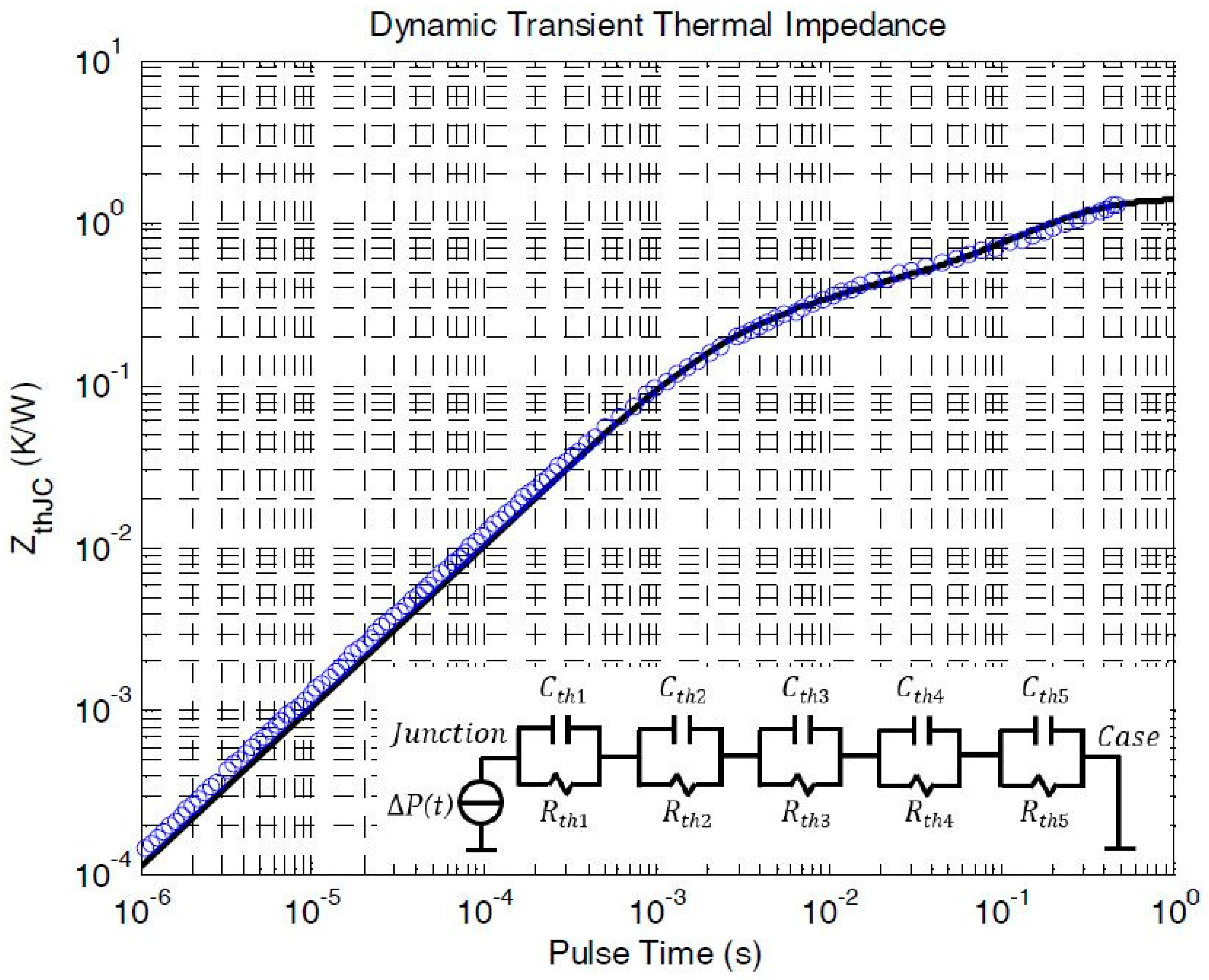
The objective of this study was to develop a simple behavioral model that includes a static I–V characteristic and nonlinear capacitance for cascode GaN FETs, and to validate the model with laboratory-fabricated cascode GaN FET devices under static and switching conditions. Leakage current and the turn-off resistance mechanism discussed in [11] for D-mode and E-mode GaN FETs were also adopted in the proposed cascode GaN FET model. The screw-threading dislocations, which may provide a conducting path in the aluminum GaN (AlGaN) layer for the leakage current, play a critical role in controlling the reverse-bias leakage current. Therefore, a thicker barrier layer could be used to suppress the leakage current [12]; in one study [13], several graded AlxGa1-xN buffer layers with different compositions were grown and compared to reduce the stress in the film and eliminate the cracks. In addition, the thermal and trapping effects are important factors describing GaN devices [14,15]. Modeling the thermal and trapping effects [16,17,18], which influence both the output linearity and output power, are of importance in practice. In Reference [16], the trapping effect was considered as an additional filter network at the gate and drain to correct for bias-dependent dispersion. In [17], a trapping and thermal phenomena related model formulation is presented. In [18], a gate and drain-lag-related trapping effects model by modifying the gate-source voltage at the input of the current source was proposed to improve the large-signal simulation results. Although a more sophisticated model that includes the thermal effects (as shown in Appendix A. Table A1 shows the fitting parameters Rth and Cth for Foster RC models. Figure A1 shows dynamic thermal impedance (Zth,JC) versus pulse width (tp) for single pulse [14].) may be applicable, the thermal effect was insignificant in the double-pulse experiment of this research. Hence, the simplified SPICE model was used instead to determine the transfer curve of GaN.
Previous studies have proposed several laboratory-fabricated GaN FETs and examined the electrical characteristics in D-mode GaN FETs and cascode devices [19]. However, none of the studies mentioned in this paper have developed a model for fabricated cascode GaN FETs. The present study was conducted in three stages. First, a metal-insulator-semiconductor high-electron-mobility transistor (MIS-HEMT) device structure with a cascode low-voltage metal–oxide–semiconductor field-effect transistor (LV MOSFET) was introduced, and electrical characterization was performed using a curve tracer and C–V analyzer [20]; second, for dynamic switching characterization, a gate charge circuit and a double-pulse tester with an inductive load were developed to evaluate the switching performance; finally, the leakage current and turn-off resistance mechanism were integrated into the cascode-type device model. With the aforementioned static and dynamic extracted parameters, experimental results were obtained using the fabricated cascode GaN FET model.
2. Materials and Methods
2.1. Device Structure of the Fabricated MIS-HEMT and Cascode Package
Figure 1a presents a simplified schematic of the fabricated AlGaN/GaN MIS-HEMT used in the experiments of this study. The parameters were as follows: Al0.23Ga0.77N layer thickness = 20 nm, GaN layer thickness = 2.1 μm, gate-to-drain spacing = 17 μm, gate-to-source spacing = 3 μm, gate length = 1 μm, gate width = 1 mm, number of fingers = 80, and total gate width = 80 mm. Details on the device fabrication can be found in [19]. A MIS-HEMT is a “normally on” device; in other words, without a negative gate-source voltage, the device channel remains in the “on” state. However, when connected to a low-voltage (LV) cascode-type MOSFET, “normally on” MIS-HEMT devices act as “normally off” devices, as shown in Figure 1b. The MIS-HEMT used in this study was a 600-V, 300-mΩ device from [19]; the selected LV MOSFET was a 30-V OptiMOSTM3 with an RDS(on) of 3.1 mΩ and a silicon carbide (SiC) Schottky barrier diode (SBD) with a 600-V, 10-A rating. The study from which the MIS-HEMT was adopted demonstrated the characteristics of laboratory-fabricated D-mode and cascode GaN FETs [19]. Although the static measured voltage rating was greater than 600 V, the test voltage used in the present study was less than 100 V because the dynamic voltage rating was associated with current collapse phenomena [21]. Moreover, because of variations in device fabrication, wire bonding, and packaging, the characteristics of the device had to be measured to obtain detailed information about the device. Many manufacturers, such as Transphorm, IR/Infineon, RFMD, and MicroGaN, announced their preliminary products of cascade GaN devices [1]. Among them, only Transphorm are off-the-shelf devices, and the product items include TPH3202, TPH3006, TPH3206, TPH3208, TPH3212, and others with different current ratings or packages. We have chosen TPH3006PS (Transphorm Inc., Goleta, CA, USA) in a TO-220 package as a benchmark to compare our cascade GaN FET fabricated in NCTU with TO-257 package [19] as both transistors had similar voltage as well as current rating and were in similar lead frame packages. A brief datasheet of TPH3006PS 2014 is included in Appendix B Table A2 [22].
Figure 2 presents the proposed SPICE model for the fabricated cascode GaN FETs, which was configured by connecting the MIS-HEMT and low-voltage MOSFET in series and the SiC SBD in antiparallel to the cascode drain-to-source terminals. The junction field-effect transistor (JFET) model was selected to simulate the MIS-HEMT, and the level-1 MOSFET model [23] was selected to simulate the LV MOSFET. SiC SBD forward current and junction capacitance parameters, which were fitted using the third quadrant of the cascode GaN FET and capacitance curves, were fitted conveniently by using the method in [24].
2.2. Static Characteristics
The static characteristics, namely the transfer characteristics (IDS–VGS), third-quadrant characteristics, and parasitic capacitance, were measured using a curve tracer [20]. Both the static characteristics and the parameters extracted using the SPICE model are discussed in the following section.
2.2.1. MIS-HEMT and LV MOSFET Transfer Curve Characteristics
The JFET model was employed to simulate the MIS-HEMT. The DC characteristics of the JFET model were defined according to the parameters VTH and β, which determine the variation in drain current, and λ, which is the channel-length modulation. Two ohmic resistances, RD and RS, were also included in the JFET model. Other parameters not noted here were set as their default values. Thus, the JFET equation in the SPICE model for the DC current is as follows:
Cutoff region: Vgs ≤ VTH,
Linear region: Vds ≤ Vgs − VTH,
Saturation region: 0 < Vgs − VTH < Vds,
A level-1 MOSFET model was employed to simulate the LV MOSFET with a model-characterized equation identical to Equations (1)–(3), with the exception of parameter β (which was replaced with 1/2 KP, where KP is the transconductance parameter and λ is the short-channel width modulation slope coefficient in the saturated region). The positive sign of VTH determines the positive threshold voltage. The threshold voltage (VTH), β, and KP can be obtained from the IDS–VGS curve (transfer characteristic), which can be extracted by using the extrapolation in the saturation region (ESR) method [24].
Figure 3a illustrates the transfer characteristics of the fabricated D-mode MIS-HEMT device when VGS = −25 to 1 V (measured in 1-V increments) with VDS = 10 V, as well as the transfer characteristics of the fabricated cascode GaN FET device when VGS = 0 to 6 V (measured in 0.1-V increments) with VDS = 10 V. The red and blue symbols in the figure represent the plots of IDS versus VGS for the fabricated D-mode and cascode devices, respectively. According to the ESR method [24], the tangent of the resulting –VGS curve was derived at the maximum slope point; then, the threshold voltage was determined by the intersection between this tangent and the horizontal axis. The parameter could be extracted from the slope of the maximum slope point on the curve. The red triangles indicate the transfer characteristic of the MIS-HEMT device. The threshold voltages given by the tangent of the –VGS (black triangles) are shown to intersect at −20 V. Additionally, the slope of the maximum slope point on the –VGS curve is shown to be 0.64; therefore, parameter β is 0.4. The blue circles show the transfer characteristic of the GaN FET device. The threshold voltages given by the tangent of the –VGS (black circles) are shown to intersect at 1.7 V. Additionally, the slope of the maximum slope point on the –VGS curve is shown to be 3.73; therefore, parameter KP is 27.8. In summary, the threshold voltage of the D-mode MIS-HEMT device was −20 V, whereas that of the cascode device was 1.7 V. In other words, the threshold voltage shifted from a negative to positive value, which is compatible with existing commercial gate drive circuits for MOSFETs.
In the present method, JFETs connected in series with ohmic resistances RD and RS were employed to simulate the MIS-HEMT in order to fit the transfer characteristic to an S-shaped curve. The dashed–dotted line in Figure 3a represents the curve with the JFETs, in which the experimentally extracted threshold voltage VTH_J = −20 V was substituted, and where β_J = 0.4 and λ_J = 0. The dashed line indicates that RS_J = 0.05, whereas the solid line indicates that RD_J = 0.13. Overall, the simulated curve is similar to the measured curve. The solid line indicates the curve derived with JFETs connected in series in a level-1 MOSFET model, in which the values for the MOSFET were experimentally extracted as follows: VTH = 1.7 V, KP = 27.8, λ = 0, RD = 0.013, and RS = 0.007. The LV MOSFET model is explained in detail in [23,26], and parameters of the JFET and level-1 MOSFET models in the fabricated GaN FET are listed in Table 1. Figure 3b presents the transfer characteristics of the commercial cascode GaN FETs [TPH3006PS], with the data for the datasheet and SPICE model obtained from the device manufacturer [22]. The value of the plateau voltage (VPL) can be predicted from the transfer characteristic graph. Notably, the simulated plateau voltage of the commercial devices was lower than that in the datasheet when the current was less than 20 A.
2.2.2. Third-Quadrant Characteristics
Because the fabricated D-mode GaN FET did not contain a body diode between the source and drain, the reverse I–V characteristics in the third quadrant are represented by the triangles in Figure 4. According to [27], the reverse drain–source voltage increased with the magnitude of the negative gate–source voltage, resulting in power loss. An additional SiC SBD with an antiparallel connection to the fabricated cascode GaN FET can not only reduce the reverse recovery time [16] but also limit the forward drop voltage under the turn-off condition (represented by the circles in Figure 4). Therefore, a negative voltage can be applied to the gate to completely turn off the GaN FET, thereby reducing the power loss and preventing a faulty turn-on [28]. The SiC SBD forward parameters were fitted by using the method in [24].
2.2.3. Parasitic Capacitances
The three-point C–V parameter extraction method [24] was employed to extract the SiC SBD junction capacitance (CD) parameters and to model the LV MOSFET gate–drain capacitance (Cgd_M), drain–source capacitance (Cds_M), and MIS-HEMT parasitic capacitance (Cgs_J1, and Cgd_J1). A 600-V, 10-A rated SiC SBD was used. The junction capacitance is presented in Figure 5a, where parameters CJ0 = 698.53 pF, VJ_CD = 0.52 V, and M_CD = 0.45. These parameters were extracted based on VDS = 1 V, which was selected at the lower voltage end of the C–V curve as point 1. Points 2 (VDS = 80 V) and 3 (VDS = 100 V) were selected at the upper voltage end of the C–V curve. The LV MOSFET Cgs0, which is the gate–source overlap capacitance per meter channel width (where W denotes the gate width), was extracted from the characteristic capacitance plot at vds = 0 by using the expression Cgs0 = Cgs_M (0). By contrast, the gate–drain capacitance (Cgd_M) was modeled using the junction capacitance of the diode and the drain–source capacitance (Cds_M) was modeled using the junction capacitance of the body diode.
A plot of the measured reverse-bias junction capacitance curve versus drain–source voltage (with each axis logarithmically scaled) was extracted using the y-axis intercept and slope to determine the values of Cds0, Cgd0, M_Cds_M, and M_Cgd_M. Figure 5b presents the log–log plot of the measured parasitic capacitance versus the drain–source voltage. The zero-bias gate–drain capacitance Cgd0 and zero-bias drain–source capacitance Cds0 were extracted from the measurements at a low drain–source bias, whereas the junction grading coefficients M_Cgd_M and M_Cds_M were extracted from the slope of the gate–drain and drain–source capacitance curves at a high drain–source bias. The built-in potentials PB_Cgd_M and PB_Cds_M were extracted from a linear interpolation of the curve. Because the D-mode MIS-HEMT did not contain body diodes between the drain and source, the N-channel JFET model without body diodes can match this condition. However, an external Cds_J capacitance was instead connected between the drain and source to represent the MIS-HEMT drain-to-source capacitance. The JFET model was used to configure the MIS-HEMT, where the JFET model included gate-to-source and gate-to-drain parasitic capacitances; that is, Cgs_J and Cgd_J were used to fit the parasitic capacitance curve. Similarly, the three-point C–V method [24] was employed to extract the capacitance parameters; the results are presented in Figure 5c. The extracted capacitance parameters for the SiC SBD, LV MOSFET, and MIS-HEMT are listed in Table 2.
2.3. Analysis of the Cascode Parasitic Capacitances
Figure 6 presents the equivalent capacitances of the cascode GaN FET used in this study. Capacitances labeled with a subscript “C,” “M,” “J,” and “D” represent the capacitances of the cascode, LV MOSFET, MIS-HEMT, and SiC SBD, respectively. The cascode parasitic capacitance values were divided into two regions: VDS_M < |VP_J| and VDS_M ≥ |VP_J|. Because the MOSFET drain–source voltage is smaller than the absolute value of the MIS-HEMT pinch-off voltage (VP_J) (VDS_M < |VP_J|), the MIS-HEMT channel is conductive due to its “normally on” characteristic. The cascode input capacitance (Ciss_C,1) is the sum of Cgs_M and Cgd_M in the LV MOSFET, and is expressed as Equation (4). The transfer capacitance (Crss_C,1) is the Cgd_M of the LV MOSFET, and is expressed as Equation (5). The conducting channel of the MIS-HEMT connects the output capacitance of the MOSFET (Coss_M) [gate–drain capacitance (Cgd_M) and drain–source capacitance (Cds_M)] in parallel with the input capacitance of the MIS-HEMT (Ciss_J) [gate–drain capacitance (Cgd_J) and gate–source capacitance (Cgs_J)] and the capacitance of the SBD diode (CD); the output capacitance (Coss_C,1) of the cascode is expressed as Equation (6).
As the drain-to-source voltage of the MOSFET (VDS_M) extends higher than the pinch-off voltage of the MIS-HEMT (VP_J) (|VP_J| ≤ VDS_M), the MIS-HEMT begins to block the voltage. At the second stage, the cascode input capacitance (Ciss_C,2) is the sum of Cgs_M and Cgd_M in series with Cds_M, Cds_J, and Cgs_J. Notably, these parameters are parallel with each other and are expressed as Equation (7). The transfer capacitance (Crss_C,2) is Cgd_M in series with Cds_J, which is expressed as Equation (8). Finally, the cascode output parasitic capacitance (Coss_C,2) is the sum of Cgd_J, CD, and Cds_J in series with Cgd_M, Cds_M, and Cgs_J1 (which are parallel with each other) and is expressed as Equation (9).
Figure 7 illustrates the measured capacitance results. Notably, the capacitance of the fabricated cascode device abruptly decreased at 20 V, which is the exact threshold voltage VTH of the MIS-HEMT and can also be considered the pinch-off voltage VP_J in the JFET model. After the parasitic capacitances of the transistors were generated, simulations were performed following the test circuit in [29] to obtain those capacitances. The measurement and simulation results exhibited excellent agreement. Moreover, the calculated values obtained based on the analysis of the cascode capacitance exhibited strong agreement with the measured values.
2.4. Dynamic Characteristics
The dynamic gate charge characteristics (VGS–QGS), leakage current (IDSS), turn-off resistance (RDS(off)), and switching performance were evaluated using a double-pulse tester and are described as follows. From the static characteristic, the plateau voltage (VPL) in the gate charge curve is read from the transfer characteristic graph with the test current, whereas the individual gate charge is derived from the parasitic capacitance curves. Gate charge information predicts switching behavior, and turn-off resistance and leakage current are estimated using the sorting method [11].
2.4.1. Gate Charge Curve (VGS–QGS)
The test fixture that was adopted to measure the gate charge curve [30,31], which can be taken from an oscilloscope, is illustrated in Figure 8. A plot of the gate-to-source voltage versus time measured on the oscilloscope can be converted to a plot of the gate-to-source voltage versus gate charge through the following relationship: QG = Ig × t. The constant gate current Ig can be constructed using Equation (10) with a PNP-type bipolar junction transistor, a Zener diode, and two resistors. The gate charge of the transistor is controlled by injecting a fixed gate current into the transistor, which renders the total gate charge proportional to the time. Plotting the gate–source voltage against the time yields the gate charge characteristic, which is determined for a fixed drain current ID and drain voltage VDD. The load resistance RL is added to set the test current.
In this test, the drain–source voltage VDD was set at 100 V and the load resistance RL was set according to the test current ID. The constant gate current Ig was set at approximately 1 mA according to Equation (4) by using a 10-V supply voltage (VCC), PNP bipolar junction transistor, 3.3-V Zener diode (VZD), 2.7-kΩ resistor (RE), and 10-kΩ resistor (RS). The gate charge of the transistor was controlled by injecting a fixed current of 1 mA into the gate. The total gate charge was proportional to the time (i.e., 1 µs of time corresponded to 1 nC of gate charge).
A comparison of the measured and simulated gate charge characteristics is presented in Figure 9. Notably, a strong correlation was observed between the results. Because a constant current of 1 mA is charged into the gate, each division of the horizontal axis can be read in nanocoulombs when the time scale is expressed in microseconds. The dynamic performance was in agreement with the gate charge results obtained using the gate charge (QG) simulation model. The Miller plateau voltage of the fabricated GaN FET was 2.8 V when the load current ID was 9 A and VDD was 100 V (Figure 9a). A total gate charge QG of 35 nC was required to reach a gate-to-source voltage VGS of 6 V, and QGS was estimated by multiplying the Miller voltage by the input capacitance Ciss (2.8 V × 4464 pf = 12.5 nC). The drain-to-gate Miller capacitance caused an increase in the flat region from 12.5 to 17.5 nC (QGD = 5 nC) (Figure 9b). Similarly, the measured plateau voltage of the commercial cascode GaN FETs approached 3.6 V when the load current ID was 10 A and VDD was 100 V. The graph shows that a gate charge QG of 8 nC was required when the commercial cascode GaN FETs was operated with a gate-to-source voltage VGS of 6 V. QGS was 3 nC and QGD was 2 nC (from 3 to 5 nC). As noted earlier regarding the transfer curve characteristic, the simulated plateau voltage of the commercial devices was lower than that provided in the datasheet when the current was less than 20 A. Therefore, at a test current of 10 A, the simulated plateau voltage of 3.3 V is actually lower than the measured 3.6 V. The inaccuracy of the transfer curve results in a deviation in the plateau voltage.
2.4.2. Switching Performance with the Double-Pulse Tester
A double-pulse tester circuit [32] was employed to evaluate the switching performance of the fabricated GaN FET. The test circuit developed in LTspice software is shown in Figure 10. The first pulse (75 μs) built up the test current in the inductor. After termination, the inductor current commutated from the device being tested to the diode; this turn-off period of the first pulse was utilized to measure the turn-off switching characteristics of the device. The second pulse (5 μs) occurred 5 μs later; here, the turn-on period was utilized to measure the turn-on switching characteristics of the device. The turn-on and turn-off switching currents were measured using a coaxial shunt [0.1 Ω (SSDN-10)] (T & M Research) [33] placed between the source terminal and ground of the transistor. A multifunction synthesizer (NF WF1945-B) (NF Corporation, Tsunashima-higashi, Japan) was also employed to generate a repetitive double-pulse signal. Two pulses with low repetition frequencies were set, and a voltage probe (P2201) was used to measure the drain-to-source voltage. A digital storage oscilloscope (Tektronix TDS2014B; 100 MHz, 1 GS/s) (Tektronix, Inc., Beaverton, OR, USA) was adopted to record the voltage and current waveforms, and the gate driver proposed in [34] was employed to drive the cascode GaN FETs. A 0–6 V gate voltage was used to switch on both the commercial and fabricated devices. Notably, the pull-up and pull-down circuits of the selected driver IC [35] are bipolar and the MOSFET transistors are parallel. Moreover, its output resistance (Rg,O: 15 Ω) was factored into the sum of the series gate resistance Rg,S, which was set at 200 Ω to enhance the switching comparisons; in other words, the turn-on path resistance and the turn-off path resistance Rg can be Rg,S + Rg,O (215 Ω).
The graphs in Figure 11 compare the experimental switching waveforms (colored lines) and simulated waveforms (black lines) derived from the fabricated cascode GaN FET model, illustrating the turn-on and turn-off switching transients of the commercial and fabricated GaN FETs. The rise and fall times of VDS and IDS were extracted as tCR and tVF (turn-on transition) and as tVR and tCF (turn-off transition) during the switching transition period. The results showed that tCR and tVF at turn-on and tVR and tCF at turn-off time were approximately 255 and 307 ns and approximately 470 and 280 ns, respectively, in the fabricated GaN FET, but approximately 140 and 240 ns and approximately 140 and 70 ns, respectively, in the commercial GaN FETs. Next, a comparison with static on-resistance Ron,stat was conducted using a curve tracer. Figure 11a depicts the ratio of dynamic on-resistance Ron,dyn to static on-resistance Ron,stat for the commercial devices with the blocking voltage set at 100 V, as well as that for the fabricated device with the blocking voltage set at approximately 90 V. The increase in the dynamic on-resistance of the commercial devices was almost zero (Ron,dyn/Ron,stat = 150 mΩ/150 mΩ = 1), whereas that of the fabricated device was approximately 6.4 times higher than its static on-resistance Ron,stat (Ron,dyn/Ron,stat = 2110 mΩ/330 mΩ = 6.4). The larger dynamic on-resistance occurred because a higher voltage was applied [14]. Nevertheless, the voltage rating of the fabricated GaN FET was still maintained below 100 V in this experiment, because a dynamic on-resistance of more than six times the static on-resistance would destroy the devices at a higher voltage. A comparison of the switching time between the commercial and fabricated devices is summarized in Table 3. Notably, parasitic inductance and dynamic on-resistance effects were not considered in the proposed model. Future research should explore these concepts in the model to discover more precise characteristics about GaN FETs for practical applications.
2.4.3. Leakage Current and Turn-Off Resistance
According to a previous study [11] on uniformity sorting methods, device uniformity can be indirectly screened by utilizing turn-off resistance with an isolated gate drive detection circuit. A 10 × (10 MΩ) probe was employed for the measurement (RL = 10 MΩ). The off-state voltage VS(off) of the commercial cascode GaN FETs was 22 V, and the waveforms of different commercial cascode GaN FET samples were uniform. The VS(off) was maintained at 22 V, yielding a leakage current of approximately 22 V/10 MΩ = 2.2 μA [34]. Figure 12 shows the results of the analysis of the leakage current that was obtained using the curve tracer. The plot of VDS versus IDSS reveals that the leakage current hold was 2.2 μA when the drain-to-source voltage was higher than 22 V. This leakage current result was approximated from uniformity sorting methods developed elsewhere [11]. VS(off) was measured after applying different drain-to-source voltages between 10 and 180 V (red circles in Figure 11). The device turn-off resistance RDS(off) was 10 MΩ, as determined through isolated gate drive detection.
By contrast, the fabricated cascode GaN FET exhibited differences in voltage levels (VS(off)). Results from other studies [11] have revealed that the lower the VS(off) values are, the closer the parasitic capacitances are to those specified on the datasheet, with the devices with the lowest VS(off) being used as test transistors. Here, the off-state voltage Vs(off) of the fabricated cascode GaN FET was 20 V, and the leakage current obtained using the curve tracer and the calculated leakage current were extremely close (20 V/3.64 MΩ = 5.5 μA). This indicates that the average leakage current in the commercial GaN FETs, which was maintained at a constant current value above 22 V (Figure 12b), was more stable than that of the fabricated GaN FET when it was maintained at a constant value above 20 V (Figure 12a). This may be because there was no additional resistance between the drain and source of the LV MOSFET (which would have caused an unstable leakage current in the fabricated device). It is doubtful that there is a high resistance of approximately 9.9 MΩ [34] connecting the drain to the source terminal of the LV MOSFET, which would act as a safety mechanism to prevent the high leakage current from the GaN FET from damaging the LV MOSFET when the LV MOSFET is in the off state.
3. Discussion
The capacitances and QGD charges of the fabricated and commercial GaN FETs are shown in Figure 13 and Table 4. The parasitic capacitance of the LV MOSFET dominates the input parasitic capacitance value and the area below the pinch-off voltage under the Crss capacitance curve region. The QGD charge below the pinch-off voltage (0–20 V) in the fabricated GaN FET was 3.52 nC (QGD,0–20 V), whereas that above the pinch-off voltage (20–100 V) was 0.14 nC (QGD,20–100 V: 3.66 nC − 3.52 nC = 0.14 nC). The ratio between QGD,0–20 V and QGD,0–100 V was approximately 96.2%. In the commercial GaN FETs, the QGD charge below the pinch-off voltage (0–20 V) was 1.60 nC, whereas that above the pinch-off voltage (20–100 V) was 0.48 nC (QGD,20–100 V: 2.08 nC − 1.60 nC = 0.48 nC). The ratio between QGD,0–20 V and QGD,0–100 V was approximately 76.9%. Thus, the parasitic capacitance of the LV MOSFET in the fabricated GaN FET should be decreased to optimize the high switching performance. Compared with the commercial devices, the fabricated GaN FET required a larger total gate charge (QG) to charge and discharge the input capacitance (Ciss) of the transistors, which resulted in slower switching. Because the input parasitic capacitance of the cascode LV MOSFET dominated the input parasitic capacitance value, the optimal LV MOSFET should be utilized. A smaller QGS is indicative of a shorter current transition period, and a smaller Miller charge QGD is indicative of a shorter voltage transition period. Therefore, GaN FETs with lower parasitic capacitance performance have fewer gate charge requirements, which enables faster switching.
4. Conclusions
A simple behavioral model was developed by applying experimentally-extracted parameters for cascode GaN FETs. This model was constructed using a level-1 MOSFET, JFET, and diode. Model parameters were based on the extracted static and dynamic characteristics. The curve fitting and three-point C–V methods facilitated extraction of the transfer characteristics and nonlinear parasitic capacitance parameter values. The JFET was used to simulate the MIS-HEMT, which closely fit the S-shaped curve of the transfer characteristic. In addition, its pinch-off voltages extracted from the threshold voltage of the MIS-HEMT distinguished where the parasitic capacitance dropped. The SPICE model was developed with the extracted parameters, and a strong agreement was observed between the LTspice-software-simulated and measured results. Furthermore, an analysis of cascode capacitance in the fabricated GaN FET indicated that the capacitance in the LV MOSFET should be reduced to optimize its high switching performance. This is because devices with lower parasitic capacitance performance have lower gate charge requirements, which enables faster switching. The turn-off resistance mechanism was introduced to obtain leakage current information. In the fabricated GaN FET, this resistance (3.64 MΩ) was approximately 0.36 times that of the commercial GaN FETs (10 MΩ). Additionally, the corresponding leakage current of the fabricated GaN FET (5.5 μA) was 2.5 times that of the commercial GaN FETs (2.2 µA). Therefore, a lower turn-off resistance results in a higher leakage current. The optimization of device fabrication, packaging, and circuit design remains challenging. Moreover, parasitic inductance and dynamic on-resistance effects were not considered in the proposed model. In subsequent research, we plan to explore the model when it is equipped with parasitic inductance and dynamic on-resistance effects, to obtain more precise characteristics about GaN FETs for practical applications.
Acknowledgments
This work was supported by the CSIST project NCSIST-103-V312 (106), Taiwan, R.O.C. The authors would like to thank Edward Yi Chang for providing the fabrication of D-Mode MIS-HEMT chips, Stone Cheng, Wei-Hua Chieng of NCTU for supporting package technology, and National Nano Device Laboratories, for their very helpful suggestions and technical support.
Author Contributions
All authors contributed equally to the manuscript. All authors designed the experiments and analyzed the data, discussed the results for the manuscript.
Conflicts of Interest
The authors declare no conflict of interest.
Appendix A
Figure A1.
Dynamic thermal impedance (Zth,JC) versus pulse width (tp) for single pulse [14].
Figure A1.
Dynamic thermal impedance (Zth,JC) versus pulse width (tp) for single pulse [14].


Table A1.
The fitting parameters Rth and Cth for Foster RC models.
| 1 | 2 | 3 | 4 | 5 | |
|---|---|---|---|---|---|
| Rth (Ω) | 0.1596 | 0.1869 | 0.2476 | 0.3043 | 0.5016 |
| Cth (F) | 0.0083 | 0.0021 | 0.2066 | 0.2065 | 0.2092 |
Appendix B
Table A2.
A brief datasheet of TPH3006PS.
| Sym. | Parameter | Test Conditions | Typ. | Unit |
|---|---|---|---|---|
| Static | ||||
| VDSS-MAX | Maximum Drain-Source Voltage | VGS = 0 V | 600 (Min) | V |
| ID25 °C | Continuous Drain Current @ TC = 25 °C | - | 17 | A |
| VGS(th) | Gate Threshold Voltage | VDS = VGS, ID = 1 mA | 1.8 | V |
| RDS(on) | Drain-Source On-Resistance (TJ = 25 °C) | VGS = 8 V, ID = 11 A, TJ = 25 °C | 0.15 | Ω |
| Dynamic | ||||
| CISS | Input Capacitance | VGS = 0 V, VDS = 100 V, f = 1 MHz | 740 | pF |
| COSS | Output Capacitance | 133 | ||
| CRSS | Reverse Transfer Capacitance | 3.6 | ||
| Qg | Total Gate Charge | VDS = 100 V, VGS = 0–4.5 V, ID = 11 A | 6.2 | nC |
| Qgs | Gate-Source Charge | 2.1 | ||
| Qgd | Gate-Drain Charge | 2.2 | ||
Appendix C
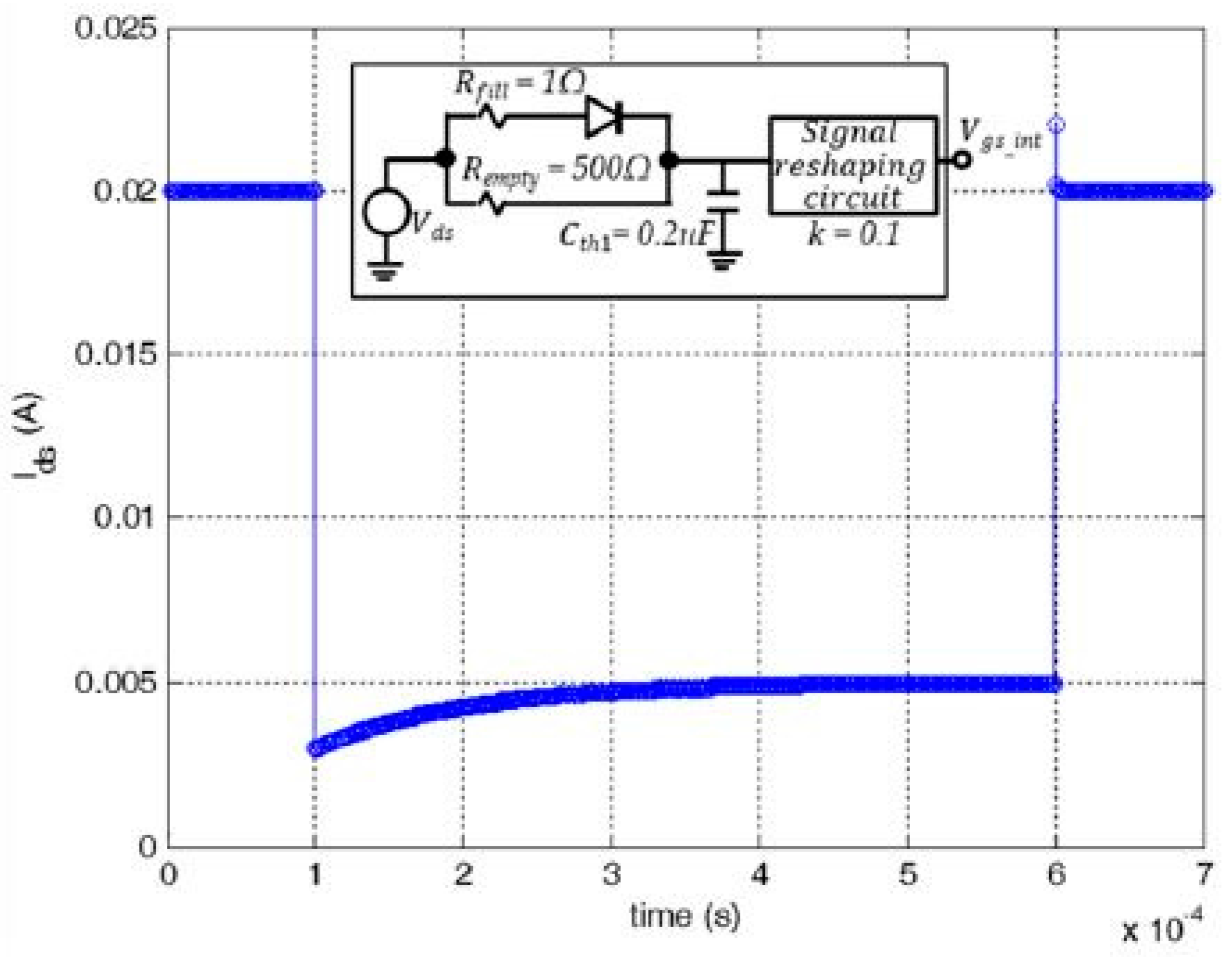
Figure A2.
Measurement to extract drain-lag [18]. (Vgs is kept at −20 V, whereas Vds is a pulse train from 30 to 10 V).
Figure A2.
Measurement to extract drain-lag [18]. (Vgs is kept at −20 V, whereas Vds is a pulse train from 30 to 10 V).
References
- Jones, E.A.; Wang, F.F.; Costinett, D. Review of Commercial GaN Power Devices and GaN-Based Converter Design Challenges. IEEE J. Emerg. Sel. Top. Power Electron. 2016, 4, 707–719. [Google Scholar] [CrossRef]
- Santi, E.; Peng, K.; Mantooth, H.A.; Hudgins, J.L. Modeling of Wide-Bandgap Power Semiconductor Devices—Part II. IEEE Trans. Electron Devices 2015, 62, 434–442. [Google Scholar] [CrossRef]
- Shah, K.; Shenai, K. Simple and accurate circuit simulation model for gallium nitride power transistors. IEEE Trans. Power Devices 2012, 59, 2735–2741. [Google Scholar] [CrossRef]
- Huang, X.; Liu, Z.; Lee, F.C.; Li, Q. Characterization and enhancement of high-voltage cascode GaN devices. IEEE Trans. Electron Devices 2015, 62, 270–277. [Google Scholar] [CrossRef]
- Ji, D.; Yue, Y.; Gao, J.; Chowdhury, S. Dynamic Modeling and Power Loss Analysis of High-Frequency Power Switches Based on GaN CAVET. IEEE Trans. Electron Devices 2016, 63, 4011–4017. [Google Scholar] [CrossRef]
- Peng, K.; Eskandari, S.; Santi, E. Characterization and modeling of a gallium nitride power HEMT. IEEE Trans. Ind. Appl. 2016, 52, 4965–4975. [Google Scholar] [CrossRef]
- Chen, K.; Zhao, Z.; Yuan, L.; Lu, T.; He, F. The impact of nonlinear junction capacitance on switching transient and its modeling for SiC MOSFET. IEEE Trans. Electron Devices 2015, 62, 333–337. [Google Scholar] [CrossRef]
- Pozo Arribas, A.; Krishnamurthy, M.; Shenai, K. A simple and accurate circuit simulation model for high-voltage SiC power MOSFETs. ECS Trans. 2014, 64, 99–110. [Google Scholar] [CrossRef]
- Lidow, A.; Strydom, J.; De Rooij, M.; Reusch, D. GaN Transistors for Efficiency Power Conversion, 2nd ed.; Power Conversion Publications: El Segundo, CA, USA, 2014; ISBN 978-1-118-84476-2. [Google Scholar]
- Wu, H.Y.; Lin, M.C.; Yang, N.Y.; Tsai, C.T.; Wu, C.B.; Lin, Y.S.; Chang, Y.C.; Chen, P.C.; Wong, K.Y.; Kwan, M.H.; et al. GaN cascode performance optimization for high efficient power applications. In Proceedings of the 28th International Symposium on Power Semiconductor Devices and ICs (ISPSD), Prague, Czech Republic, 12–16 June 2016; pp. 255–258. [Google Scholar]
- Jeng, S.L.; Wu, C.C.; Chieng, W.H. Gallium Nitride Electrical Characteristics Extraction and Uniformity Sorting. J. Nanomater. 2015, 2015, 1–15. [Google Scholar] [CrossRef]
- Wong, Y.Y.; Chang, E.Y.; Yang, T.H.; Chang, J.R.; Ku, J.T.; Hudait, M.K.; Chou, W.C.; Chen, M.; Lin, K.L. The roles of threading dislocations on electrical properties of AlGaN/GaN heterostructure grown by MBE. J. Electrochem. Soc. 2010, 157, H746–H749. [Google Scholar] [CrossRef]
- Hsiao, Y.L.; Lu, L.C.; Wu, C.H.; Chang, E.Y.; Kuo, C.I.; Maa, J.S.; Lin, K.L.; Luong, T.T.; Huang, W.C.; Chang, C.H.; et al. Effect of Graded AlxGa1-xN Layers on the Properties of GaN Grown on Patterned Si Substrates. Jpn. J. Appl. Phys. 2012, 51. [Google Scholar] [CrossRef]
- Chen, S.H.; Chou, P.C.; Cheng, S. Evaluation of thermal performance of packaged GaN HEMT cascode power switch by transient thermal testing. Appl. Therm. Eng. 2016, 98, 1003–1012. [Google Scholar] [CrossRef]
- Chou, P.C.; Chen, S.H.; Hsieh, T.E.; Cheng, S.; del Alamo, J.A.; Chang, E.Y. Evaluation and Reliability Assessment of GaN-on-Si MIS-HEMT for Power Switching Applications. Energies 2017, 10, 233. [Google Scholar] [CrossRef]
- King, J.B.; Brazil, T.J. A GaN HEMT equivalent circuit model with novel approach to dispersion modelling. In Proceedings of the IEEE Microwave Integrated Circuits Conference (EuMIC), Amsterdam, The Netherlands, 29–30 October 2012; pp. 68–71. [Google Scholar]
- Raffo, A.; Bosi, G.; Vadala, V.; Vannini, G. Behavioral modeling of GaN FETs: A load-line approach. IEEE Trans. Microw. Theory Tech. 2014, 62, 73–82. [Google Scholar] [CrossRef]
- Jardel, O.; De Groote, F.; Reveyrand, T.; Jacquet, J.C.; Charbonniaud, C.; Teyssier, J.P.; Didier, F.; Quere, R. An electrothermal model for AlGaN/GaN power HEMTs including trapping effects to improve large-signal simulation results on high VSWR. IEEE Trans. Microw. Theory Tech. 2007, 55, 2660–2669. [Google Scholar] [CrossRef]
- Chou, P.C.; Cheng, S. Performance characterization of gallium nitride HEMT cascode switch for power conditioning applications. Mater. Sci. Eng. B Adv. 2015, 198, 43–50. [Google Scholar] [CrossRef]
- Agilent Technologies. Agilent B1505A Power Device Analyzer/Curve Tracer, Step by Step Measurement Handbook for Power MOSFET. Available online: www.agilent.com (accessed on 4 August 2011).
- Ishibashi, T.; Okamoto, M.; Hiraki, E.; Tanaka, T.; Hashizume, T.; Kikuta, D.; Kachi, T. Experimental Validation of Normally-On GaN HEMT and Its Gate Drive Circuit. IEEE Trans. Ind. Appl. 2015, 51, 2415–2422. [Google Scholar] [CrossRef]
- Transphorm. TPH3006PS Datasheet. Available online: http://www.transphormusa.com/sites/default/files/public/TPH3006PS.pdf (accessed on 30 December 2014).
- Description of the ON Semiconductor MOSFET Model. Application Note AND9033, Semiconductor Components Industries, LLC, 2011. November 2011—Rev. 1. Available online: https://www.onsemi.cn/PowerSolutions/document/AND9033-D.PDF (accessed on 1 November 2011).
- Russell, H.T., Jr. The SPICE Diode Model. In Rectifier Applications Handbook; Roehr, W.D., Ed.; November 2001; Ch. 3; pp. 47–71. Available online: http://www.introni.it/pdf/Motorola%20-%20Rectifier%20Applications%20Handbook.pdf (accessed on 2 November 2001).
- Hsieh, T.E.; Lin, Y.C.; Liao, J.T.; Lan, W.C.; Chin, P.C.; Chang, E.Y. Effect of high voltage stress on the DC performance of the Al2O3/AlN GaN metal-insulator-semiconductor high-electron mobility transistor for power applications. Appl. Phys. Express 2015, 8, 104102. [Google Scholar] [CrossRef]
- Arribas, A.P.; Shang, F.; Krishnamurthy, M.; Shenai, K. Simple and accurate circuit simulation model for SiC power MOSFETs. IEEE Trans. Electron Devices 2015, 62, 449–457. [Google Scholar] [CrossRef]
- Umegami, H.; Hattori, F.; Nozaki, Y.; Yamamoto, M.; Machida, O. A novel high-efficiency gate drive circuit for normally off-type GaN FET. IEEE Trans. Ind. Appl. 2014, 50, 593–599. [Google Scholar] [CrossRef]
- Wang, J.; Chung, H.S.H. A novel RCD level shifter for elimination of spurious turn-on in the bridge-leg configuration. IEEE Trans. Power Electron. 2015, 30, 976–984. [Google Scholar] [CrossRef]
- Broadmeadow, M.A. Characterisation of the Cascode Gate Drive of Power MOSFETs in Clamped Inductive Switching Applications. Ph.D. Thesis, Department of Electrical and Electronic Engineering, Queensland University, Brisbane, Australia, 2015. [Google Scholar]
- ON Semiconductor. MOSFET Gate-Charge Origin and Its Applications, AND9083/D Datasheet, February 2016—Rev. 2. Available online: onsemi.com (accessed on 2 February 2016).
- Yiin, A.J.; Schrimpf, R.D.; Galloway, K.F. Gate-Charge Measurements for Irradiated N-Channel DMOS Power Transistors. IEEE Trans. Nucl. Sci. 1991, 38, 1352–1358. [Google Scholar] [CrossRef]
- Chen, Z. Characterization and Modeling of High-Switching-Speed Behavior of SiC Active Devices. Master’s Thesis, Department of Electrical and Electronic Engineering, Virginia Tech, Blacksburg, VA, USA, 2009. [Google Scholar]
- T & M Research, 0.1 Ω (SSDN-414-10), SDN Series Current Viewing Resistors. Available online: www.tandmresearch.com (accessed on 13 March 2015).
- Wu, C.C.; Jeng, S.L. Switching performance of GaN FETs in terms of turn-off resistance characteristics an experimental study. In Proceedings of the 2016 4th International Conference on Electrical & Electronics Engineering and Computer Science (ICEEECS 2016), Jinan, China, 15–16 October 2016; Volume 50, pp. 546–551. [Google Scholar]
- Texas Instruments. Single 9-A High-Speed Low-Side MOSFET Driver. Available online: www.ti.com/product/UCC27322 (accessed on 12 October 2015).
Figure 1.
Schematic of the (a) metal-insulator-semiconductor high-electron-mobility transistor. (MIS-HEMT) (“normally on”) and (b) cascode GaN field-effect transistor (FET).
Figure 1.
Schematic of the (a) metal-insulator-semiconductor high-electron-mobility transistor. (MIS-HEMT) (“normally on”) and (b) cascode GaN field-effect transistor (FET).
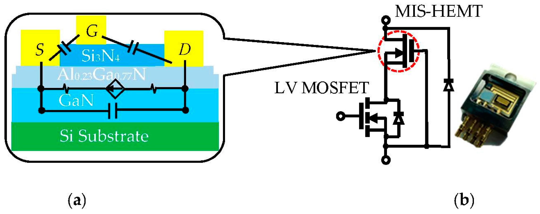
Figure 2.
Fabricated cascode GaN FET simulation program with integrated circuit emphasis (SPICE) model. The approximations introduced by the adopted model for the I–V characteristics from ref [18] were added into the model. The corresponding gain k, Rfill, Rempty, and the capacitance C were obtained from the trapping effect example in Appendix C Figure A2.

Figure 3.
Transfer characteristics of (a) fabricated D-mode (red triangle) and cascode (blue circle) GaN FETs (the solid line indicates the SPICE simulation); (b) commercial cascode GaN FETs [TPH3006PS]; and (c) fabricated D-mode before (red triangle) and after high-voltage (100 V) stress (blue triangle) GaN FETs (the solid line indicates the SPICE simulation) [25].
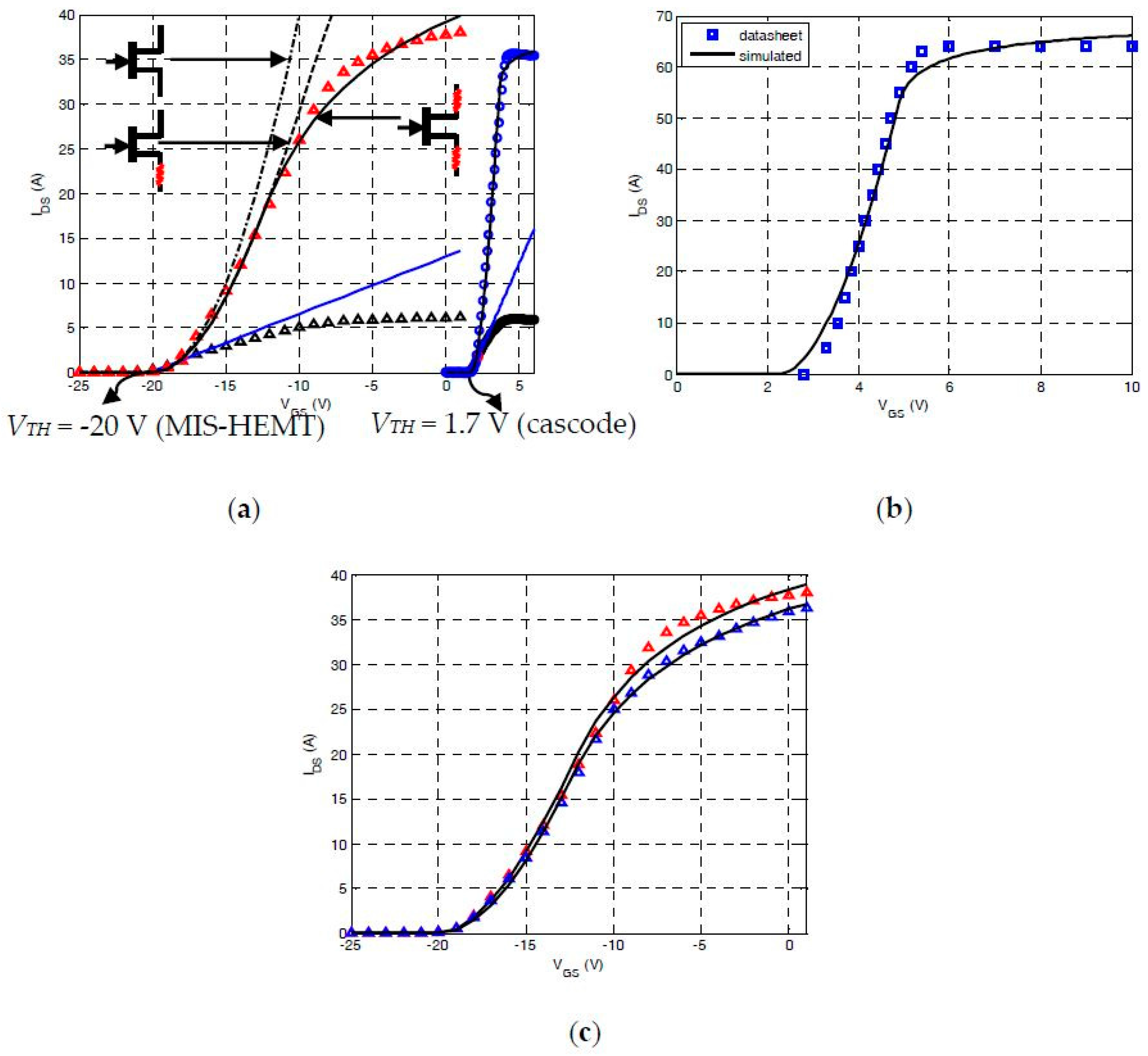
Figure 4.
Third-quadrant characteristics of the fabricated D-mode (triangles) and cascode (circles) GaN FETs (black solid line: simulation).
Figure 4.
Third-quadrant characteristics of the fabricated D-mode (triangles) and cascode (circles) GaN FETs (black solid line: simulation).
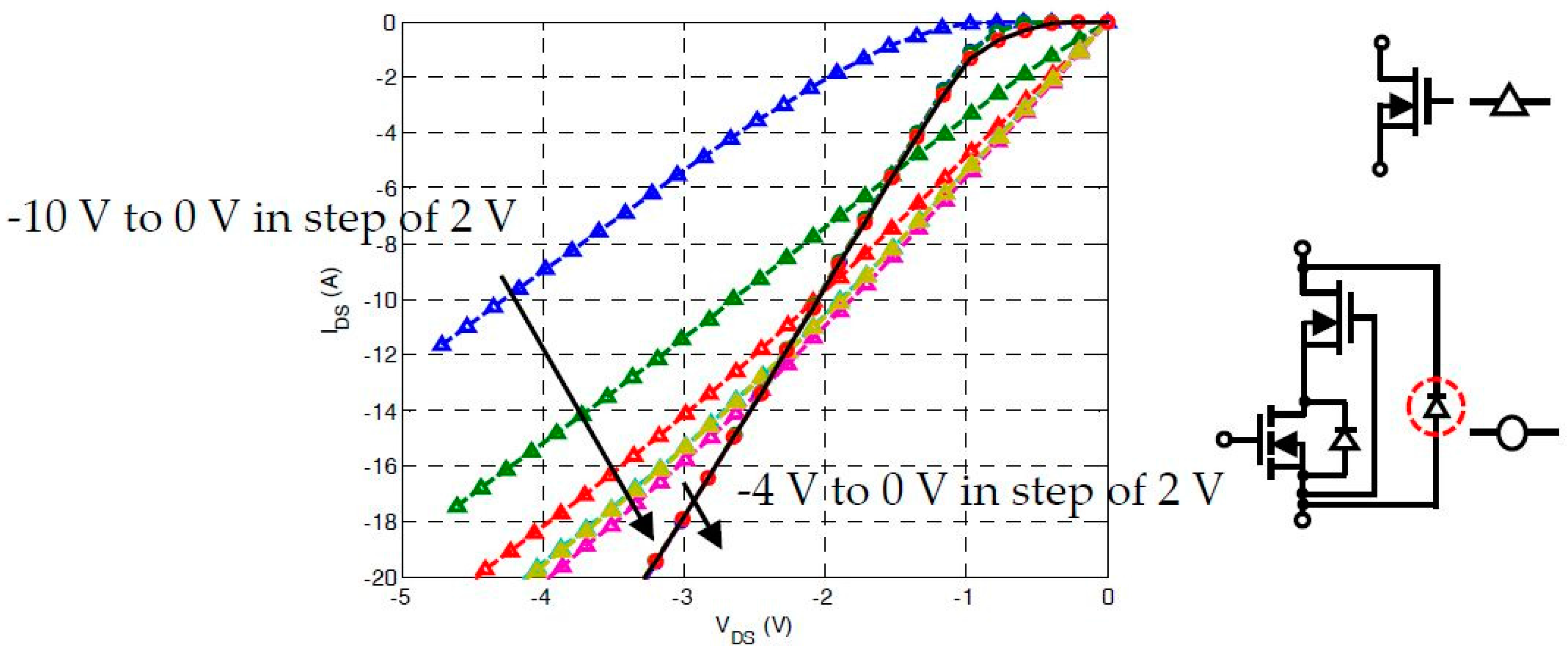
Figure 5.
Log–log plot of the (a) parasitic capacitance for the silicon carbide (SiC) Schottky barrier diode (SBD) versus the drain–source voltage (square: measured, solid line: simulation); (b) parasitic capacitance for the low-voltage (LV) MOSFET versus the drain–source voltage (circle: measured, solid line: simulation); and (c) parasitic capacitance of the MIS-HEMT versus the drain–source voltage (triangle: measured, solid line: simulation).

Figure 6.
Equivalent capacitances of the fabricated cascode GaN FET.

Figure 7.
Parasitic capacitance of the fabricated GaN FETs (colored lines: measured, black line: simulation, circle: calculated).
Figure 7.
Parasitic capacitance of the fabricated GaN FETs (colored lines: measured, black line: simulation, circle: calculated).
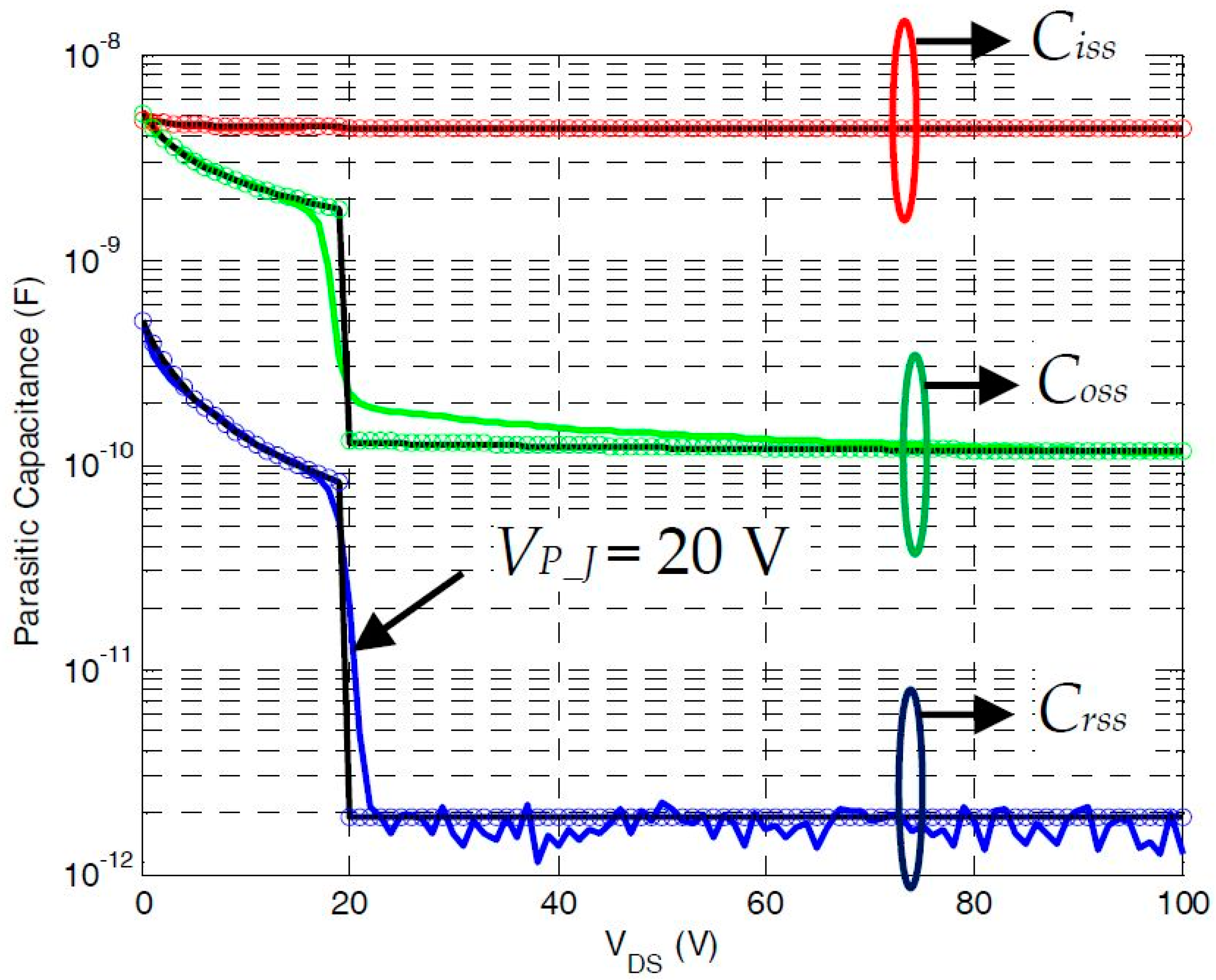
Figure 8.
Test circuit for the gate charge measurements. Gate current Ig was set to 1 mA by using the constant current source.
Figure 8.
Test circuit for the gate charge measurements. Gate current Ig was set to 1 mA by using the constant current source.

Figure 9.
Gate-to-source voltage (VGS) versus total gate charge (QG) of the (a) fabricated GaN FET and (b) commercial GaN FETs [TPH3006PS].
Figure 9.
Gate-to-source voltage (VGS) versus total gate charge (QG) of the (a) fabricated GaN FET and (b) commercial GaN FETs [TPH3006PS].
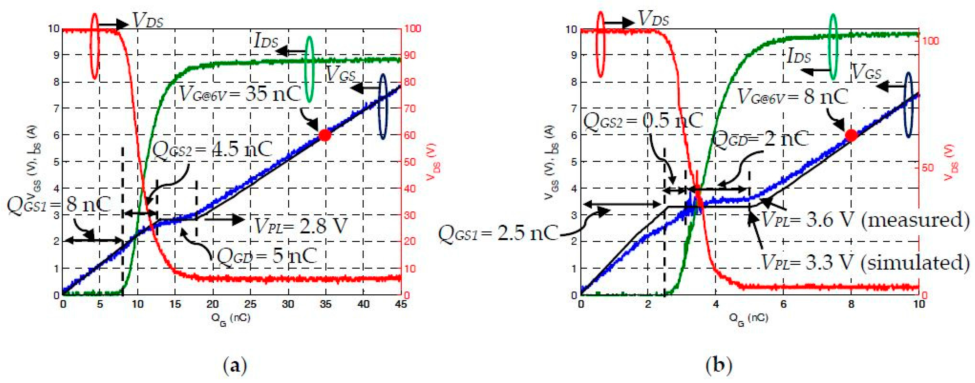
Figure 10.
Double-pulse test circuit (a) in the LTspice program for simulation and (b) used in the experiment.
Figure 10.
Double-pulse test circuit (a) in the LTspice program for simulation and (b) used in the experiment.
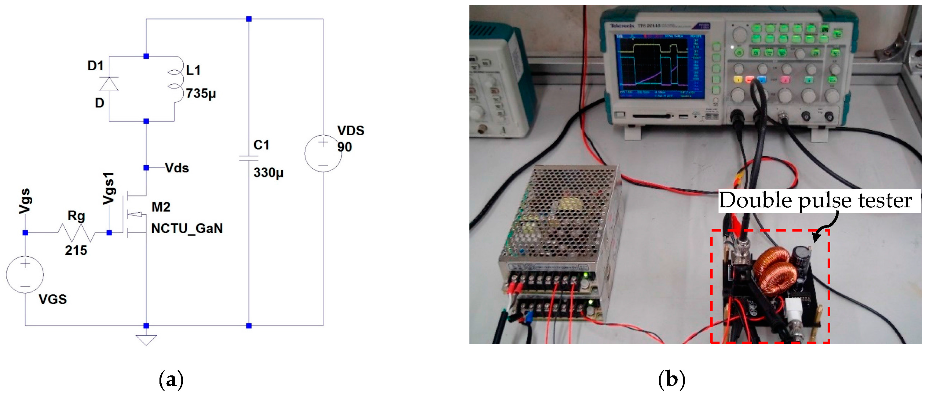
Figure 11.
(a) Turn-on and (b) turn-off switching transients of the commercial [TPH3006PS] (fine colored lines) and fabricated (bold colored lines) GaN FETs (Simulation: black line).
Figure 11.
(a) Turn-on and (b) turn-off switching transients of the commercial [TPH3006PS] (fine colored lines) and fabricated (bold colored lines) GaN FETs (Simulation: black line).

Figure 12.
Leakage current (IDSS) versus drain-to-source voltage (VDS) in the (a) fabricated GaN FET and (b) commercial GaN FETs [TPH3006PS].
Figure 12.
Leakage current (IDSS) versus drain-to-source voltage (VDS) in the (a) fabricated GaN FET and (b) commercial GaN FETs [TPH3006PS].
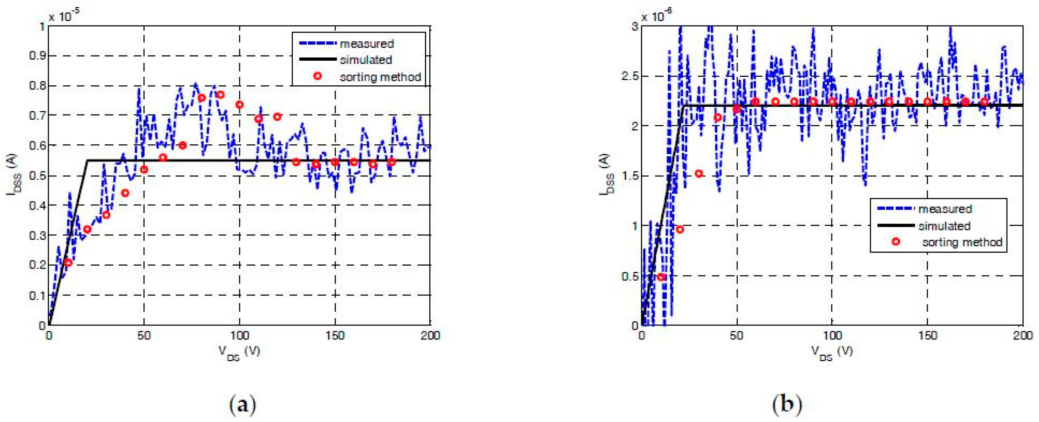
Figure 13.
Comparison of fabricated and commercial GaN FETs [TPH3006PS] regarding (a) capacitances and (b) QGD charges. (Dashed line: commercial GaN FETs, solid line: fabricated GaN FET).
Figure 13.
Comparison of fabricated and commercial GaN FETs [TPH3006PS] regarding (a) capacitances and (b) QGD charges. (Dashed line: commercial GaN FETs, solid line: fabricated GaN FET).
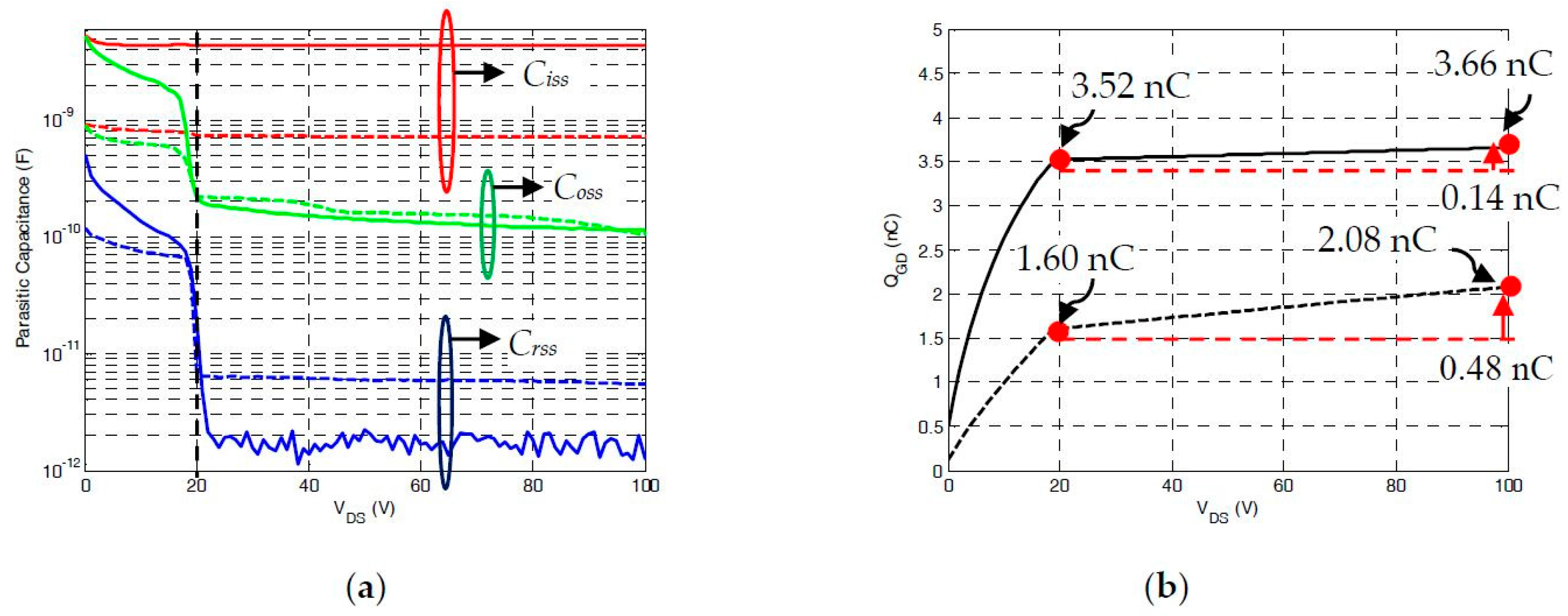
Table 1.
Parameters of the junction field-effect transistor (JFET) and level-1 metal–oxide–semiconductor field-effect transistor (MOSFET) models in the fabricated GaN FET.
Table 1.
Parameters of the junction field-effect transistor (JFET) and level-1 metal–oxide–semiconductor field-effect transistor (MOSFET) models in the fabricated GaN FET.
| Parameter | Model | Area | β | VTH | λ | RS | RD | |
|---|---|---|---|---|---|---|---|---|
| MIS-HEMT | JFET | 1 | 0.4/0.39 * | −20 | 0/−0.001 * | 0.05 | 0.13/0.15 * | |
| Parameter | Model | W(μ) | L(μ) | KP | VTH | λ | RS | RD |
| LV MOSFET | Lev.1 MOS | 100 | 100 | 27.8 | 1.7 | 0 | 0.007 | 0.013 |
* Parameters after high-voltage (100 V) stress [25].
Table 2.
Extracted capacitance parameters of the SiC SBD, LV MOSFET, and MIS-HEMT.
| SiC SBD | LV MOSFET | MIS-HEMT | |||||||
|---|---|---|---|---|---|---|---|---|---|
| Par. | CJ0 (pF) | VJ (V) | M | CJ0 (pF) | PB (V) | M | CJ0 (pF) | VJ (V) | M |
| CD | 698.53 | 0.52 | 0.45 | - | - | ||||
| Cgs | - | Cgs0 (pF) × W (μ) = 4350 | 44.25 | 25.90 | −0.03 | ||||
| Cgd | - | 368.55 | 95.95 | 8.92 | 15.42 | 15.69 | 0.24 | ||
| Cds | - | 422.14 | 180.75 | 12.04 | 45.17 | 39.97 | 0.06 | ||
Table 3.
Switching time and energy loss between the fabricated and commercial GaN FETs [TPH3006PS].
| Fabricated | Commercial | ||
|---|---|---|---|
| Turn-on | Current rise time (tCR) (ns) | 255 | 140 |
| Voltage fall time (tVF) (ns) | 307 | 240 | |
| Turn-off | Voltage rise time (tVR) (ns) | 470 | 140 |
| Current fall time (tCF) (ns) | 280 | 70 | |
| RDS(ON) (mΩ) | Static on-resistance Ron,stat | 330 | 150 |
| Dynamic on-resistance Ron,dyn | 2110 | 150 | |
| Ron,dyn/Ron,stat ratio | 6.4 | 1 | |
Table 4.
Comparison of the parasitic capacitances and charges between the commercial and fabricated GaN FETs [TPH3006PS].
Table 4.
Comparison of the parasitic capacitances and charges between the commercial and fabricated GaN FETs [TPH3006PS].
| Parameter | Fabricated Cascode | Commercial Cascode | |||
|---|---|---|---|---|---|
| QGS (nC) | QGS1 | 12.5 | 8 | 3 | 2.5 |
| QGS2 | 4.5 | 0.5 | |||
| QGD (nC) | 5 | 2 | |||
| QG (nC) | 35 @ 6 V | 8 @ 6 V | |||
| RDS(ON) (mΩ) | 330 | 150 | |||
| FOM | 3135 | 375 | |||
| QGD,0–20 V | 3.52 | 1.60 | |||
| QGD,0–100 V | 3.66 | 2.08 | |||
| QGD,0–20 V/GD,0–100 V | 96.2% | 76.9% | |||
Figure of Merit (FOM) = (QGS2 + QGD) × RDS(ON) (10−12 Ω × C).
© 2017 by the authors. Licensee MDPI, Basel, Switzerland. This article is an open access article distributed under the terms and conditions of the Creative Commons Attribution (CC BY) license (http://creativecommons.org/licenses/by/4.0/).
Share and Cite
MDPI and ACS Style
Wu, C.-C.; Jeng, S.-L. Simulation Model Development for Packaged Cascode Gallium Nitride Field-Effect Transistors. Crystals 2017, 7, 250. https://doi.org/10.3390/cryst7080250
AMA Style
Wu C-C, Jeng S-L. Simulation Model Development for Packaged Cascode Gallium Nitride Field-Effect Transistors. Crystals. 2017; 7(8):250. https://doi.org/10.3390/cryst7080250
Chicago/Turabian StyleWu, Chih-Chiang, and Shyr-Long Jeng. 2017. "Simulation Model Development for Packaged Cascode Gallium Nitride Field-Effect Transistors" Crystals 7, no. 8: 250. https://doi.org/10.3390/cryst7080250
Note that from the first issue of 2016, this journal uses article numbers instead of page numbers. See further details here.