
Interfacial Kinetics of Efficient Perovskite Solar Cells
by
Pankaj Yadav
1,*, 
Daniel Prochowicz
1,2,
Michael Saliba
1,
Pablo P. Boix
3,
Shaik M. Zakeeruddin
1 and
Michael Grätzel
1 1
Laboratory of Photonics and Interfaces, Institute of Chemical Sciences and Engineering, School of Basic Sciences, Ecole Polytechnique Fédérale de Lausanne (EPFL), CH-1015 Lausanne, Switzerland
2
Institute of Physical Chemistry, Polish Academy of Sciences, Kasprzaka 44/52, 01-224 Warsaw, Poland
3
Instituto de Ciencia Molecular, Universidad de Valencia, C/Catedrático J. Beltrán 2, 46980 Paterna, Spain
*
Author to whom correspondence should be addressed.
Crystals 2017, 7(8), 252; https://doi.org/10.3390/cryst7080252
Submission received: 9 June 2017
/
Revised: 30 July 2017
/
Accepted: 3 August 2017
/
Published: 13 August 2017
(This article belongs to the Special Issue Metal Halide Perovskite Crystals: Growth Techniques, Properties and Emerging Applications)
Abstract
:Perovskite solar cells (PSCs) have immense potential for high power conversion efficiency with an ease of fabrication procedure. The fundamental understanding of interfacial kinetics in PSCs is crucial for further improving of their photovoltaic performance. Herein we use the current-voltage (J-V) characteristics and impedance spectroscopy (IS) measurements to probe the interfacial kinetics on efficient MAPbI3 solar cells. We show that series resistance (RS) of PSCs exhibits an ohmic and non-ohmic behavior that causes a significant voltage drop across it. The Nyquist spectra as a function of applied bias reveal the characteristic features of ion motion and accumulation that is mainly associated with the MA cations in MAPbI3. With these findings, we provide an efficient way to understand the working mechanism of perovskite solar cells.
1. Introduction
Organic lead halide-based perovskite solar cells (PSCs) have shown an unprecedented rise in their efficiency from 2% to more than 22% in just a few years [1,2,3,4]. This fast increase in efficiency and low temperature fabrication procedure makes perovskites potential candidates for low-cost photovoltaic devices. The most commonly employed PSC structure consists of a mesoporous electron transport layer such as TiO2, followed by perovskite absorber layer and spiro-OMeTAD as a hole transport layer. Various attempts have been made to alter the morphological and structural properties of the hole transporting material (HTM), the absorber material, and electron transporting layer (ETL) to enhance the device performance [5,6,7]. In spite of the advances in device efficiency and architecture, many aspects of device processes occurring at the bulk (inside) and interfaces are still lagging behind. It has been established that the perovskite absorber material behaves as a mixed electronic-ionic conductor, in which electronic and ionic charges are influenced by applied bias rate, temperature, and illumination [8,9,10,11]. Therefore, obtaining exact information on the role of electronic and ionic components as well as their contributions to the device performance is crucial for the further in-depth understanding of the working mechanism of solar cells.
Another aspect that seems to play a significant role in power deliverability is the presence of J-V hysteresis. The surface treatments of ETL, HTL, and the perovskite absorber layer by light metals and carbonaceous materials doping have shown a positive impact in the mitigation of hysteresis behavior [12,13,14,15,16,17,18]. Most studies consider only ionic movement as the phenomenon responsible for J-V hysteresis. In fact, under illumination and applied bias, both the components, i.e., electronic and ionic components define the performance of PSCs. It is believed that the presence of ions can change the transport and recombination of electronic charge carriers or vice-versa. In this context, the goal of resolving the responses from ionic and electronic components in relation with the PSC device configuration represents a relevant aspect of the device performance.
Here, we present a semi-quantitative model of a PSC (represented by MAPbI3) that can explain specific issues related to the interfaces and bulk properties of PSCs by considering the coupled responses of electronic and ionic components using impedance spectroscopy (IS). This technique allows us to deconvulate the responses from the both the interfaces and bulk region of the PSC. The well-defined dependencies of Nyquist spectra as a function of applied bias determine the resistive and capacitive parameters, and more importantly resolve the accumulation and movement of ions. Moreover, the presented model permits the quantification of prominent voltage loss sources. On the basis of IS and current-voltage extracted resistive, capacitive, and associated time responses, we postulate that in the investigated solar cell the predominant slow time response is caused by ion motion.
2. Theoretical Background
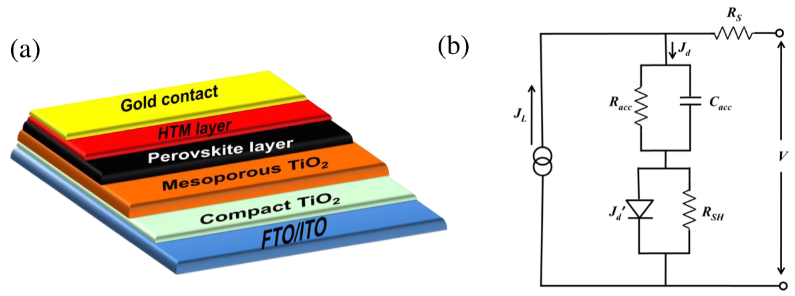
In general, PSCs consist of a mesoporous or planar electron transport layer, a perovskite absorber layer, a hole transport layer, and gold and fluorine-doped tin oxide (FTO) as a back and front contact, respectively (Figure 1a). Under illumination, photogenerated charges, i.e., electrons and holes, were collected at the FTO and gold contacts via the electron and hole transport layers. It is important to recognize that along with the photo generation, transportation, and recombination of charge carriers, the mobile ions and charge defects can also move and cause the screening of a built-in electric field [19,20,21,22]. Recent studies have shown that the accumulation of the ions and vacancies at interfaces changes the interfacial charge concentration and recombination rates, as well as the net photovoltage by setting up an electrostatic potential in addition to the built-in potential [23,24,25]. Since the electrostatic and built-in potentials have the same polarity (backward scan), the net open circuit voltage (VOC) of PSC devices is the sum of these potentials [24,26].
A generalized single diode model of a PSC, including the built-in and electrostatic potential formed due to the accumulation of ions and charges, is placed in a model previously discussed by Gottesman and others (Figure 1b) [24,26,27]. In this model, the dark current carrier recombination in the bulk and space charge region (SCR) is represented by a diode equation , where q, are the elementary charge and applied voltage, is the reverse saturation dark current, and and T are the Boltzman constant and cell temperature, respectively. The ideality factor (m) for a single diode falls in the range between , where m1 signifies the top of the barrier transport (barrier for holes in ETL and for electrons in HTL) and m 2 signifies the Shockley-Read Hall (SRH) as a dominant recombination mechanism. In some cases, the ideality factor m is greater than 2, and this behavior is ascribed to the nonlinear shunt resistances across the junctions and/or a significant voltage drop across ETL and HTL [28]. The voltage drop across a diode has the form of . Under an open circuit voltage condition, J 0 and V VOC = Vd + Vacc shows that the open-circuit voltage (VOC) of a PSC is defined as the sum of the two potentials in series.
Considering the fact that the accumulation mechanism is due to the electronic and ionic contributions, the accumulation resistance may contain the information about the recombination and ionic components. The alternating current (AC) electrical equivalent circuit shown in Figure 1b is driven through the variable direct current (DC) source in parallel with the AC signal generator. The circuit is also demonstrated as the generalized circuit for the impedance spectra analysis. The low frequency spectra of IS is modeled through and (also denoted as RLf and CLf in the IS section). In PSCs, it is well established that the movement of ions can take place across the active layer, and this diffusion is generally defined by the Warburg element (w) depending upon the IS spectra.
3. Results and Discussion
3.1. Device Characterization
The J-V characteristic of the PSC under 1 Sun (AM 1.5 G) at 25 °C in a backward direction scan is shown in Figure 2a (for the film characterization and device fabrication procedure, see supplementary material. The PSC depicts an impressive power conversion efficiency (PCE) of 17.3% with an open circuit voltage (VOC) of 1.07 V, a short circuit current density of 21.6 mA/cm2, and a fill factor of 75%. In order to determine the diode characteristic parameters, i.e., (m and J0), we carried out the VOC vs. illumination (0.1 to 100 mW/cm2) measurements (Figure 2b). In the plot, the symbol represents the experimental data points and the line is defined by using the expression . The value of m = 1.7 and J0 = 1.4 × 10¹³ A/cm2 was obtained using the diode equation. The fabricated PSC also exhibits an efficient charge transport under working conditions, as JSC vs. illumination power law coefficient is almost equal to 1 (see Figure S3).
3.2. Impedance Spectroscopy
The electrochemical impedance spectroscopy (IS) of a PSC as a function of applied bias (from 0 V to VOC) under illumination at room temperature is shown in Figure 3. The AC modulation voltage of 20 mV and frequency in the range of 1 MHz to 200 mHz was used. The obtained Nyquist spectra are fitted with the electrical equivalent circuit discussed by Zarazúa et al. [29]. The error in experimental and theoretical data is within the acceptable limit of <1%. The IS spectra in the low forward bias follow the description of the two parallel resistor-capacitor (RC) components connected in series, while the values of each individual pair is different in magnitude. The shown spectra exhibit a maximum value of Z′ and Z′′ because, in this probed bias range (0–0.4 V), the net response of the diode is mainly dominated by and geometrical capacitance (Cg). In turn, the IS curves at voltage of 0.3 V to 0.6 V are composed of a depressed semicircle in the high frequency region and a straight line in the low frequency region (Figure 3b). When the bias voltages are higher than the knee voltage, the radii of the semicircle in the high frequency region also decreases; however, the straight line in the low frequency region converts into a semicircle arc (Figure 3c). Figure 3e–f demonstrate the general complex Nyquist spectra exhibiting the Warburg features evident by the linear line at 45° at the low frequency region, wherein the dashed line shows the expected behavior of a blocking electrode. Meanwhile, IS spectra exhibiting the double layer characteristics are evident by the semicircular arc present in the low frequency regime.
As the applied bias gradually increases beyond the knee voltage, the radii of the high frequency semicircles decreases at a faster rate and the low frequency line is converted to a semicircle arc. The rate of change in the low and high frequency responses under applied bias is shown in Figure 3d (the arrow indicates the transients between semicircles to straight lines). We found that the rate of change in the low frequency arc is faster than the corresponding rate in the high frequency arc. This implies that under the influence of illumination, the coupled influence of charge and ion movement may cause a higher rate of decrease in the low frequency region. In comparison to the electronic conductors such as thin-film solar cells, the low frequency region of IS was defined by the recombination resistance and chemical capacitance. We remark that due to very thin perovskite absorber layer (~200 nm) and ion motion, the chemical capacitance that is usually masked by the electrostatic capacitance arises due to ion accumulation. It is also worth noting that these two kinds of capacitances (i.e., chemical and low frequency capacitance) are totally different in their nature.
The RS of a PSC extracted from the high frequency intercept on the x-axis as a function of applied bias is shown in Figure 4a. The RS vs. applied bias plot in the range of 0.0 to 0.4 V depicts a constant value of Rs (13.8 Ω), which may arise from the ohmic components of the PSC. In turn, in the range of 0.4 to 0.8 V, the plot of Rs shows a peak that can be attributed to non-ohmic components of the solar cell. The presence of this peak is commonly observed in silicon and dye-sensitized solar cells [30,31,32], however, to the best of our knowledge, such behavior has not yet been reported in PSCs. We note that the physical origin of the peak is not fully clear, but can be attributed to the formation of a low Schottky barrier at the perovskite/HTM interface and a voltage drop across the diode that varies with bias, as shown in Figure 4a (blue line). Therefore, it is necessary to develop a proper strategy that allows a reduction of the value of RS in PSCs.
A comparative plot of the total resistance calculated from IS and the differential resistance from J-V characteristics measured under 1 sun illumination is shown in Figure 4b. In the plot, the symbol represents the extracted resistance, i.e., (RS + RHf + RLf) from IS, and the line represents from the J-V curve. We found that the values obtained from both IS and J-V exhibit a similar bias dependence. The plot of RHf and RLf with respect to V + JRS is shown in Figure S4 of SI. It should be noted that the magnitude and rate of change for RHf is lower than that observed for RLf under the probed range of bias. The value of RHf varies from 250 Ω to 10 Ω and, at the same time, the corresponding value of RLf diminishes from 1 KΩ to 1 Ω, signifying the differences in their sources of origin. The value of RLf, which is associated with the charge accumulation and/or recombination in PSCs, was further examined by the determination of a potential drop across VLf, where. It has been found that is varied in the range of 100 mV to 50 mV, in a bias range from 0.8 V to Voc. More recently, the illumination of PSCs under different time periods and voltage decay periods revealed the formation of electrostatic potential in the range of 100 mV–150 mV in series with built-in potential [24,33]. These results illustrate that the non-ohmic RS may be associated with the voltage drop across the HTL/perovskite interface. Moreover, the bias dependence of RLf and the associated VLf could explain the accumulation of charges and ions at the ETL/perovskite interface, as well as cause a build-up of potential.
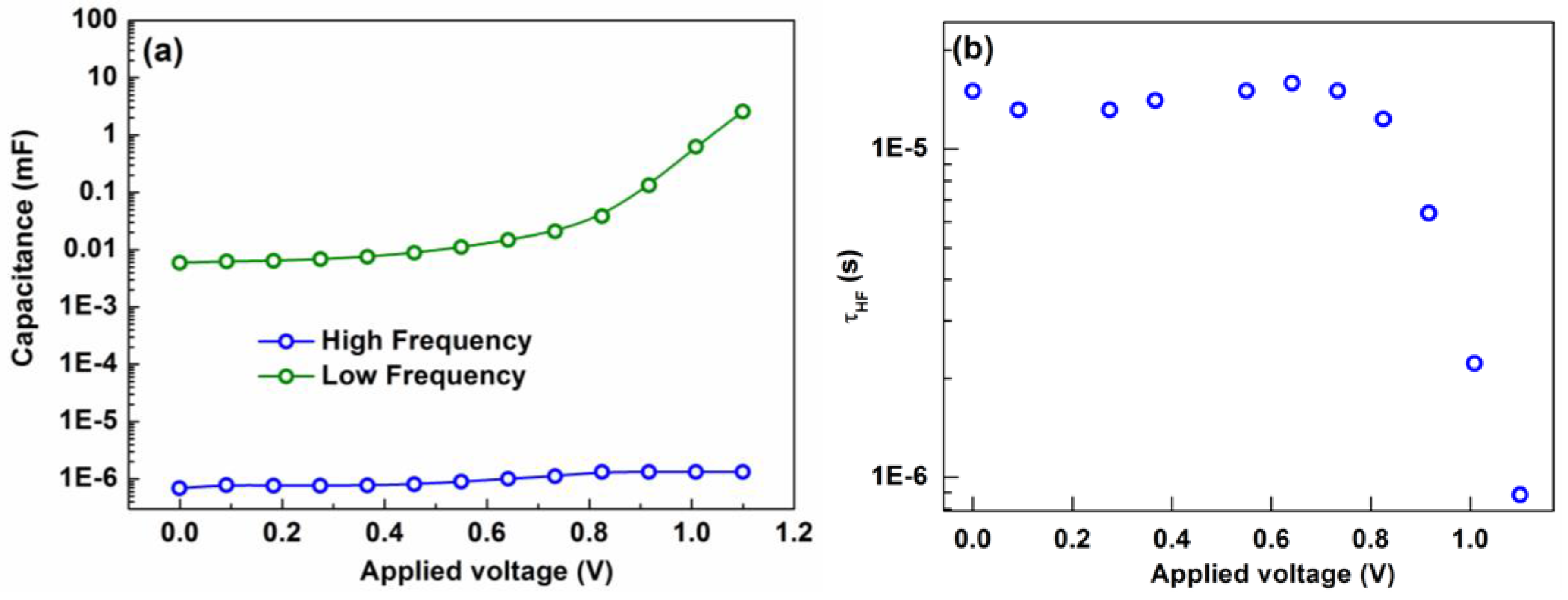
As it is outlined in the theoretical section, the high frequency capacitance related to the polarizability of the perovskite absorber layer is defined by geometrical capacitance (Cg). However, the low frequency capacitance is defined by electrostatic capacitance (Cs). The variation of Cg and Cs in the bias range from knee voltage to VOC of a PSC is shown in Figure 5a. In the low forward bias, Cg depicts the constant value in the order of 1 μF at a frequency of 10 KHz. The Cg plot seems to be constant, while CS increases exponentially. Considering the parallel plate capacitance as with d = 200 nm and permittivity of the free space, is obtained. The obtained value of is comparable with the previously reported values by other authors [9]. On the other hand, CS exhibits a value in order of mF measured at 1 Hz.
A Mott-schottky (MS) plot of a PSC at the frequency of 10 KHz in the bias range from 0 V to VOC is shown in Figure S5. The MS plot clearly shows the bias dominance of Cg in the low bias range and of CS beyond the knee voltage. As compared to silicon solar cells, where the MS plot is generally defined by the three distinguishable capacitances, i.e., Cg, CS, and depletion layer capacitance (Cdl), the obtained MS plot for the PSC was only defined by Cg and CS. The fit of CS with respect to the bias gives the value of built-in potential (intercept) and defect density (slope). The obtained value of the built-in potential Vbi = 0.1 V and the defect density of 10−17 cm−3 are consistent with the reported values for MAPbI3-based solar cells [33].
Time constants corresponding to the high and low frequency spectra as a function of applied bias are shown in Figure 5b and Figure S6. We observed that the high frequency time response (τHf) under applied bias follows the decreasing trend of RHf (not CHf). Therefore, this time constant cannot be considered as a characteristic response of any physical processes in the PSC. From the low frequency region, a bias independent time constant (τLf) in the order of 1s was obtained. Similar values of slow time constants were also observed by other groups using intensity modulated voltage spectroscopy, open circuit voltage decay, and voltage and current transient techniques [24,25,26,27] The mechanism relies on long-lived trapping without recombination, and trap-assisted recombination was assigned for such a long response time, which seems to be anomalously long. It is well known that the presence of traps in a semiconductor accelerates the recombination process that in turn decreases the response time. As the low frequency capacitance has a dielectric nature, the corresponding time constant cannot be considered as a recombination lifetime. In general, IS response under illumination in the frequency range of 1 MHz–200 mHz requires a 3–4 min per voltage scan (considering an average of two data errors for each frequency), which is more than sufficient to accumulate the holes and cations at the TiO2/perovskite interface and to contribute to the electrostatic potential. Considering the fact that the efficiently fast relaxation phenomenon is generally associated with the charge carriers, the low frequency relaxation time (τLf) can be assigned to the motion of ions required to reach the equilibrium. A similar observation was also drawn by Gottesman et al. by using the open circuit voltage decay method [24]. The authors demonstrated that VOC in a PSC occurs in two steps, where the fast decay of the built-in potential happens instantly, but the electrostatic potential caused by charge and ion accumulation can take tens of minutes to return its steady-state condition [24]. Moreover, it was also shown that MA+ has a large polarization relaxation time in the range of 1–100 s [34]. Therefore, one can correlate the long τLf to the relaxation time of MA+ ions.
4. Conclusions
We have presented a semi-quantitative model that can elucidate the bulk and interfacial characteristics of PSCs. Our results strongly suggest that the low frequency impedance response of a PSC depends on its ionic movements. The ionic movements in the PSC were detected by probing the IS response as a function of applied bias. The presented results also revealed that, in comparison to electronic conductors where the low frequency response of IS was defined by recombination resistance and chemical capacitance, the chemical capacitance in PSCs (mix-conductors) is masked by the electrostatic capacitance that arises from ion accumulation. In addition, we showed that the series resistance (RS) of a PSC exhibits an ohmic and non-ohmic behavior that causes a significant voltage drop across them. Our conclusion regarding the ion accumulation is supported by the bias dependence of RLf and the associated VLf that could explain the accumulation of charges and ions at the ETL/perovskite interface. The slow relaxation time (τLf) in a PSC can be assigned to the motion of ions required to reach the equilibrium.
Supplementary Materials
The following are available online at https://www.mdpi.com/2073-4352/7/8/252/s1, Figure S1: UV:Vis absorption spectra of MAPbI3 perovskite absorber layer, Figure S2: (a) Surface and (b) Cross sectional SEM morphology of MAPbI3 perovskite absorber layer, Figure S3: Current Density of the device measured under various illumination levels where the net photocurrent is constant, (b) from mid forward bias to knee voltage, Figure S4: The variation of high and low frequency resistance as a function of V+JRS , Figure S5: A Mott-schottky (MS) plot of PSC at the frequency of 10 KHz in the bias range from 0 V to VOC, Figure S6: Variation of low frequency time constant as a function of applied bias for PSC.
Author Contributions
P.Y. conceived and designed the experiments; D.P. and M.S. performed the experiments; P.Y. and P.P.B. analyzed the data; P.P.B. contributed analysis tools; P.Y. and D.P. wrote the paper, S.M.Z and M.Z. supervised the project.
Conflicts of Interest
The authors declare no conflict of interest.
References
- Chen, W.; Wu, Y.; Yue, Y.; Liu, J.; Zhang, W.; Yang, X.; Chen, H.; Bi, E.; Ashraful, I.; Grätzel, M.; et al. Efficient and stable large-area perovskite solar cells with inorganic charge extraction layers. Science 2015, 350, 944–948. [Google Scholar] [CrossRef] [PubMed]
- Im, J.-H.; Lee, C.-R.; Lee, J.-W.; Park, S.-W.; Park, N.-G. 6.5% efficient perovskite quantum-dot-sensitized solar cell. Nanoscale 2011, 3, 4088–4093. [Google Scholar] [CrossRef] [PubMed]
- Kojima, A.; Teshima, K.; Shirai, Y.; Miyasaka, T. Organometal halide perovskites as visible-light sensitizers for photovoltaic cells. J. Am. Chem. Soc. 2009, 131, 6050–6051. [Google Scholar] [CrossRef] [PubMed]
- Liu, M.; Johnston, M.B.; Snaith, H.J. Efficient planar heterojunction perovskite solar cells by vapour deposition. Nature 2013, 501, 395–398. [Google Scholar] [CrossRef] [PubMed]
- Chang, C.-Y.; Chang, Y.-C.; Huang, W.-K.; Liao, W.-C.; Wang, H.; Yeh, C.; Tsai, B.-C.; Huang, Y.-C.; Tsao, C.-S. Achieving high efficiency and improved stability in large-area ITO-free perovskite solar cells with thiol-functionalized self-assembled monolayers. J. Mater. Chem. A 2016, 4, 7903–7913. [Google Scholar] [CrossRef]
- Feng, S.; Yang, Y.; Li, M.; Wang, J.; Cheng, Z.; Li, J.; Ji, G.; Yin, G.; Song, F.; Wang, Z.; et al. High-Performance Perovskite Solar Cells Engineered by an Ammonia Modified Graphene Oxide Interfacial Layer. ACS Appl. Mater. Interfaces 2016, 8, 14503–14512. [Google Scholar] [CrossRef] [PubMed]
- Bai, Y.; Dong, Q.; Shao, Y.; Deng, Y.; Wang, Q.; Shen, L.; Wang, D.; Wei, W.; Huang, J. Enhancing stability and efficiency of perovskite solar cells with crosslinkable silane-functionalized and doped fullerene. Nat. Commun. 2016, 7, 12806. [Google Scholar] [CrossRef] [PubMed]
- Heo, J.H.; Song, D.H.; Han, H.J.; Kim, S.Y.; Kim, J.H.; Kim, D.; Shin, H.W.; Ahn, T.K.; Wolf, C.; Lee, T.-W.; et al. Planar CH3NH3PbI3 Perovskite Solar Cells with Constant 17.2% Average Power Conversion Efficiency Irrespective of the Scan Rate. Adv. Mater. 2015, 27, 3424–3430. [Google Scholar] [CrossRef] [PubMed]
- Nie, W.; Blancon, J.-C.; Neukirch, A.J.; Appavoo, K.; Tsai, H.; Chhowalla, M.; Alam, M.A.; Sfeir, M.Y.; Katan, C.; Even, J.; et al. Light-activated photocurrent degradation and self-healing in perovskite solar cells. Nat. Commun. 2016, 7, 11574. [Google Scholar] [CrossRef] [PubMed] [Green Version]
- Unger, E.L.; Hoke, E.T.; Bailie, C.D.; Nguyen, W.H.; Bowring, A.R.; Heumuller, T.; Christoforo, M.G.; McGehee, M.D. Hysteresis and transient behavior in current– voltage measurements of hybrid-perovskite absorber solar cells. Energy Environ. Sci. 2014, 7, 3690–3698. [Google Scholar] [CrossRef]
- Heo, J.H.; Han, H.J.; Kim, D.; Ahn, T.K.; Im, S.H. Hysteresis-less inverted CH3NH3PbI3 planar perovskite hybrid solar cells with 18.1% power conversion efficiency. Energy Environ. Sci. 2015, 8, 1602–1608. [Google Scholar] [CrossRef]
- Zhou, Z.; Huang, L.; Mei, X.; Zhao, Y.; Lin, Z.; Zhen, H.; Ling, Q. Highly reproducible and photocurrent hysteresis-less planar perovskite solar cells with a modified solvent annealing method. Sol. Energy 2016, 136, 210–216. [Google Scholar] [CrossRef]
- Kim, J.; Teridi, M.A.M.; Yusoff, A.R.B.M.; Jang, J. Stable and null current hysteresis perovskite solar cells based nitrogen doped graphene oxide nanoribbons hole transport layer. Sci. Rep. 2016, 6, 27773. [Google Scholar] [CrossRef] [PubMed]
- Heo, J.H.; Im, S.H. Highly reproducible, efficient hysteresis-less CH3NH3PbI3−xClx planar hybrid solar cells without requiring heat-treatment. Nanoscale 2016, 8, 2554–2560. [Google Scholar] [CrossRef] [PubMed]
- Xu, J.; Buin, A.; Ip, A.H.; Li, W.; Voznyy, O.; Comin, R.; Yuan, M.; Jeon, S.; Ning, Z.; McDowell, J.J.; et al. Perovskite–fullerene hybrid materials suppress hysteresis in planar diodes. Nat. Commun. 2015, 6, 7081. [Google Scholar] [CrossRef] [PubMed]
- Giordano, F.; Abate, A.; Baena, J.P.C.; Saliba, M.; Matsui, T.; Im, S.H.; Zakeeruddin, S.M.; Nazeeruddin, M.K.; Hagfeldt, A.; et al. Enhanced electronic properties in mesoporous TiO2 via lithium doping for high-efficiency perovskite solar cells. Nat. Commun. 2016, 7, 10379. [Google Scholar] [CrossRef] [PubMed]
- Kwon, U.; Kim, B.-G.; Nguyen, D.C.; Park, J.-H.; Ha, N.Y.; Kim, S.-J.; Ko, S.H.; Lee, S.; Lee, D.; Park, H.J. Solution-processible crystalline NiO nanoparticles for high-performance planar perovskite photovoltaic cells. Sci. Rep. 2016, 6, 30759. [Google Scholar] [CrossRef] [PubMed]
- Yang, G.; Wang, C.; Lei, H.; Zheng, X.; Qin, P.; Xiong, L.; Zhao, X.; Yan, Y.; Fang, G. Interface engineering in planar perovskite solar cells: energy level alignment, perovskite morphology control and high performance achievement. J. Mater. Chem. A 2017, 5, 1658–1666. [Google Scholar] [CrossRef]
- Armin, A.; Juska, G.; Philippa, B.W.; Burn, P.L.; Meredith, P.; White, R.D.; Pivrikas, A. Doping-induced screening of the built-in-field in organic solar cells: Effect on charge transport and recombination. Adv. Energy Mater. 2013, 3, 321–327. [Google Scholar] [CrossRef]
- Belisle, R.A.; Nguyen, W.H.; Bowring, A.R.; Calado, P.; Li, X.; Irvine, S.J.C.; McGehee, M.D.; Barnes, P.R.F.; O’Regan, B.C. Interpretation of inverted photocurrent transients in organic lead halide perovskite solar cells: proof of the field screening by mobile ions and determination of the space charge layer widths. Energy Environ. Sci. 2017, 10, 192–204. [Google Scholar] [CrossRef]
- Eames, C.; Frost, J.M.; Barnes, P.R.F.; O’Regan, B.C.; Walsh, A.; Islam, M.S. Ionic transport in hybrid lead iodide perovskite solar cells. Nat. Commun. 2015, 6, 7497. [Google Scholar] [CrossRef] [PubMed] [Green Version]
- Calado, P.; Telford, A.M.; Bryant, D.; Li, X.; Nelson, J.; O’Regan, B.C.; Barnes, P.R.F. Evidence for ion migration in hybrid perovskite solar cells with minimal hysteresis. Nat. Commun. 2016, 7, 13831. [Google Scholar] [CrossRef] [PubMed]
- Yu, H.; Lu, H.; Xie, F.; Zhou, S.; Zhao, N. Native defect-induced hysteresis behavior in organolead iodide perovskite solar cells. Adv. Funct. Mater. 2016, 26, 1411–1419. [Google Scholar] [CrossRef]
- Gottesman, R.; Lopez-Varo, P.; Gouda, L.; Jimenez-Tejada, J.A.; Hu, J.; Tirosh, S.; Zaban, A.; Bisquert, J. Dynamic phenomena at perovskite/electron-selective contact interface as interpreted from photovoltage decays. Chem 2016, 1, 776–789. [Google Scholar] [CrossRef]
- Domanski, K.; Roose, B.; Matsui, T.; Saliba, M.; Turren-Cruz, S.-H.; Correa-Baena, J.-P.; Carmona, C.R.; Richardson, G.; Foster, J.M.; de Angelis, F.; et al. Migration of cations induces reversible performance losses over day/night cycling in perovskite solar cells. Energy Environ. Sci. 2017, 10, 604–613. [Google Scholar] [CrossRef]
- Ravishankar, S.; Almora, O.; Echeverría-Arrondo, C.; Ghahremanirad, E.; Aranda, C.; Guerrero, A.; Fabregat-Santiago, F.; Zaban, A.; Garcia-Belmonte, G.; Bisquert, J. Surface polarization model for the dynamic hysteresis of perovskite solar cells. J. Phys. Chem. Lett. 2017, 8, 915–921. [Google Scholar] [CrossRef] [PubMed]
- Ludmila, C.; Satoshi, U.; Piyankarage, V.V.J.; Shoji, K.; Yasutake, T.; Jotaro, N.; Takaya, K.; Hiroshi, S. Simulation of current–voltage curves for inverted planar structure perovskite solar cells using equivalent circuit model with inductance. Appl. Phys. Express 2017, 10, 025701. [Google Scholar]
- Agarwal, S.; Seetharaman, M.; Kumawat, N.K.; Subbiah, A.S.; Sarkar, S.K.; Kabra, D.; Namboothiry, M.A.G.; Nair, P.R. On the uniqueness of ideality factor and voltage exponent of perovskite-based solar cells. J. Phys. Chem. Lett. 2014, 5, 4115–4121. [Google Scholar] [CrossRef] [PubMed]
- Zarazua, I.; Han, G.; Boix, P.P.; Mhaisalkar, S.; Fabregat-Santiago, F.; Mora-Seró, I.; Bisquert, J.; Garcia-Belmonte, G. Surface Recombination and Collection Efficiency in Perovskite Solar Cells from Impedance Analysis. J. Phys. Chem. Lett. 2016, 7, 5105–5113. [Google Scholar] [CrossRef] [PubMed]
- Yadav, P.; Tripathi, B.; Pandey, K.; Kumar, M. Recombination kinetics in a silicon solar cell at low concentration: electro-analytical characterization of space-charge and quasi-neutral regions. Phys. Chem. Chem. Phys. 2014, 16, 15469–15476. [Google Scholar] [CrossRef] [PubMed]
- Yadav, P.; Pandey, K.; Tripathi, B.; Kumar, C.M.; Srivastava, S.K.; Singh, P.K.; Kumar, M. An effective way to analyse the performance limiting parameters of poly-crystalline silicon solar cell fabricated in the production line. Sol. Energy 2015, 122, 1–10. [Google Scholar] [CrossRef]
- Garland, J.E.; Crain, D.J.; Roy, D. Utilization of electrochemical impedance spectroscopy for experimental characterization of the diode features of charge recombination in a dye sensitized solar cell. Electrochim. Acta 2014, 148, 62–72. [Google Scholar] [CrossRef]
- Almora, O.; Aranda, C.; Mas-Marzá, E.; Garcia-Belmonte, G. On Mott-Schottky analysis interpretation of capacitance measurements in organometal perovskite solar cells. Appl. Phys. Lett. 2016, 109, 173903. [Google Scholar] [CrossRef]
- Leguy, A.M.A.; Frost, J.M.; McMahon, A.P.; Sakai, V.G.; Kockelmann, W.; Law, C.; Li, X.; Foglia, F.; Walsh, A.; O’Regan, B.C.; et al. The dynamics of methylammonium ions in hybrid organic–inorganic perovskite solar cells. Nat. Commun. 2015, 6, 7124. [Google Scholar] [CrossRef] [PubMed] [Green Version]
Figure 1.
Schematic representation of (a) a perovskite solar cell (PSC) and (b) a single diode model of a PSC.
Figure 1.
Schematic representation of (a) a perovskite solar cell (PSC) and (b) a single diode model of a PSC.

Figure 2.
(a) Dark and light J-V characteristics of the MAPbI3 PSC recorded under standard test conditions and (b) open circuit voltage of the device measured under various illumination levels.
Figure 2.
(a) Dark and light J-V characteristics of the MAPbI3 PSC recorded under standard test conditions and (b) open circuit voltage of the device measured under various illumination levels.
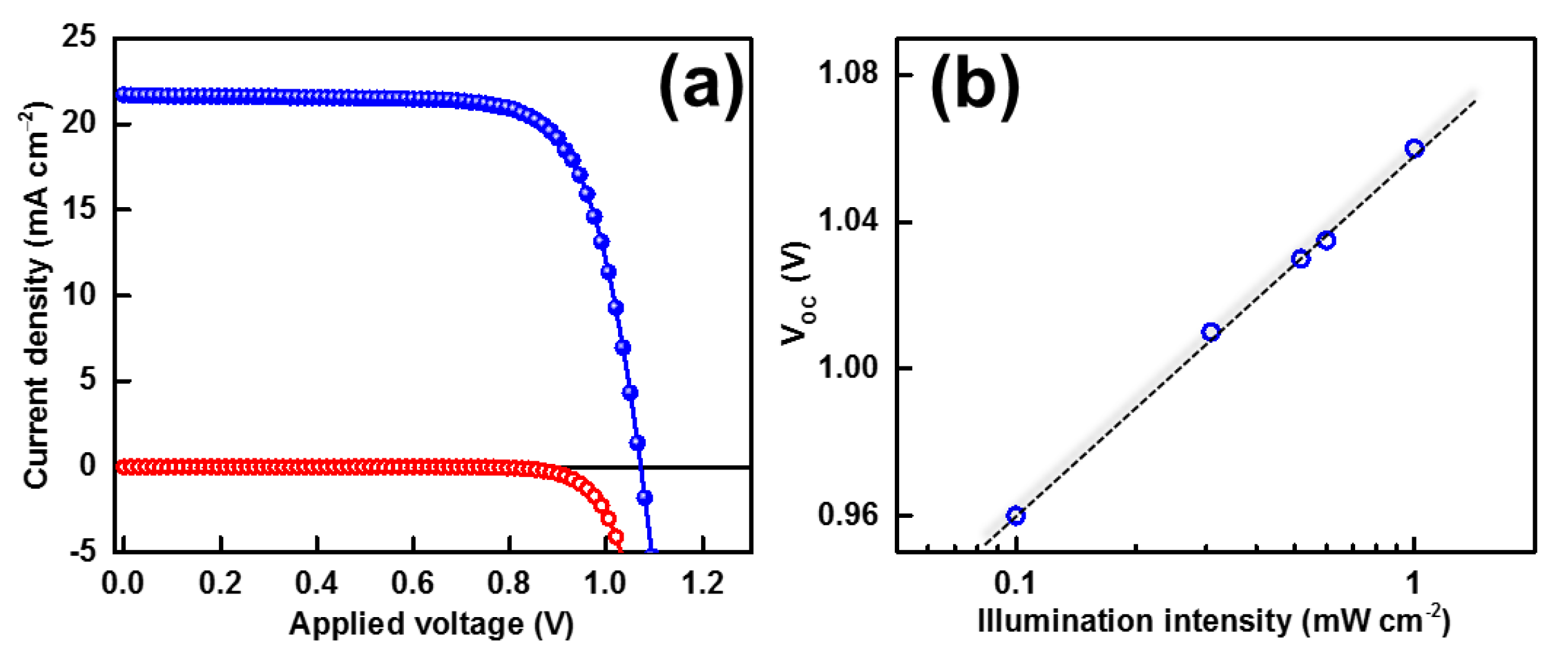
Figure 3.
Nyquist spectra of a PSC recorded at various applied biases under illumination: (a) at low forward bias where the net photocurrent is constant (see Figure 2a), (b) from mid forward bias to knee voltage, and (c) beyond knee voltage towards open circuit voltage. (d) 3D plot of Nyquist spectra covering the whole range of the applied forward bias. Here, the straight arrow indicates an increase in the low frequency arc at the low forward bias, while the curved arrow shows where the low frequency arc is converted to a straight line at the mid forward bias. (e) Typical complex Nyquist spectra exhibiting the Warburg features evident by the linear line at 45° at the low frequency region, wherein the dashed line shows the expected behavior of a blocking electrode. (f) Typical complex Nyquist spectra exhibiting the double layer characteristics evident by the semicircular arc in the low frequency regime.
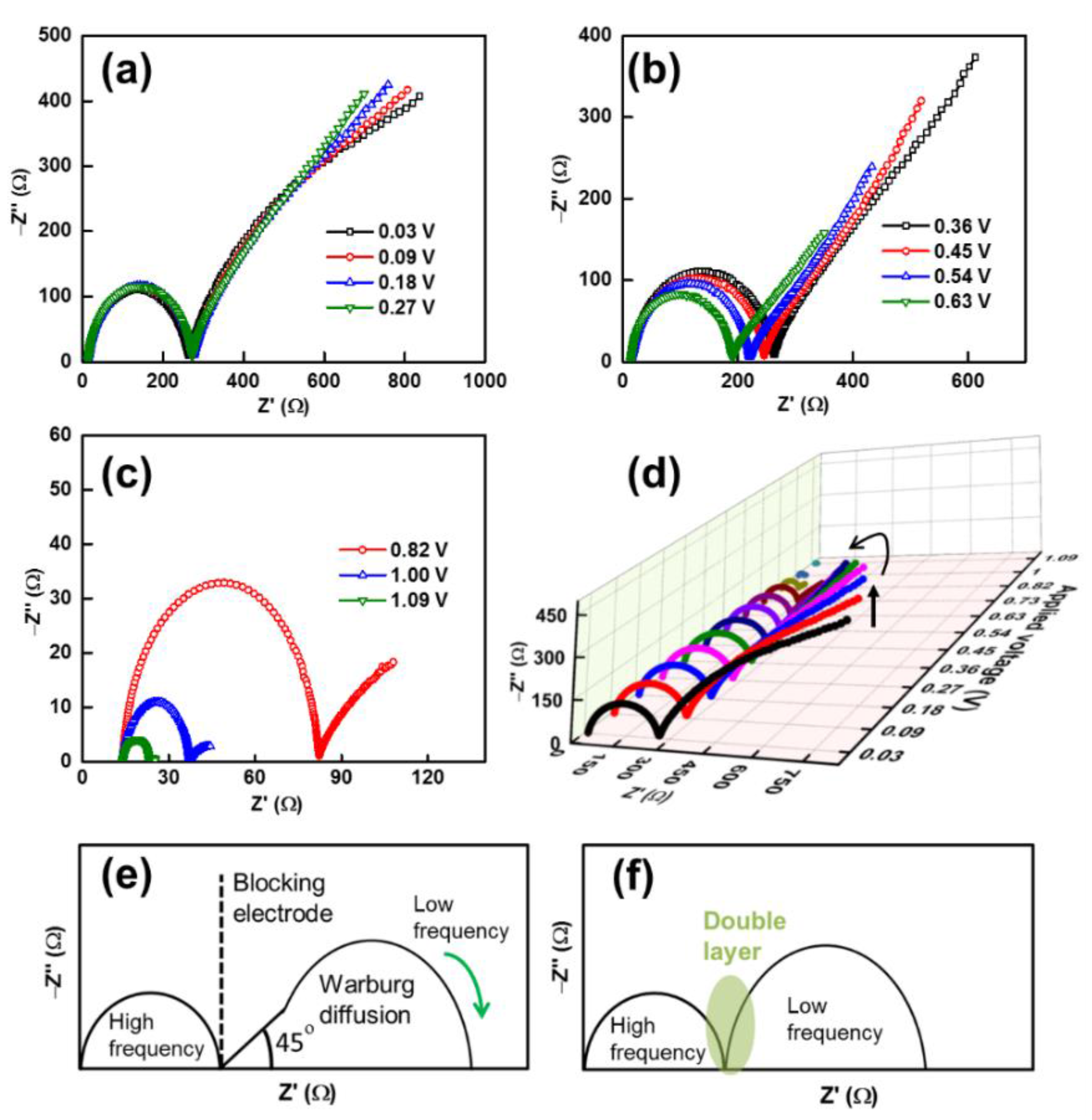
Figure 4.
(a) Variation of series resistance RS depicted from the impedence spectroscopy (IS) measurements, and the voltage drop at RS under 1 sun illumination as a function of applied bias. (b) A comparative plot of total resistance calculated from IS and differential resistance from J-V characteristics measured under 1 sun illumination as a function of applied voltage.
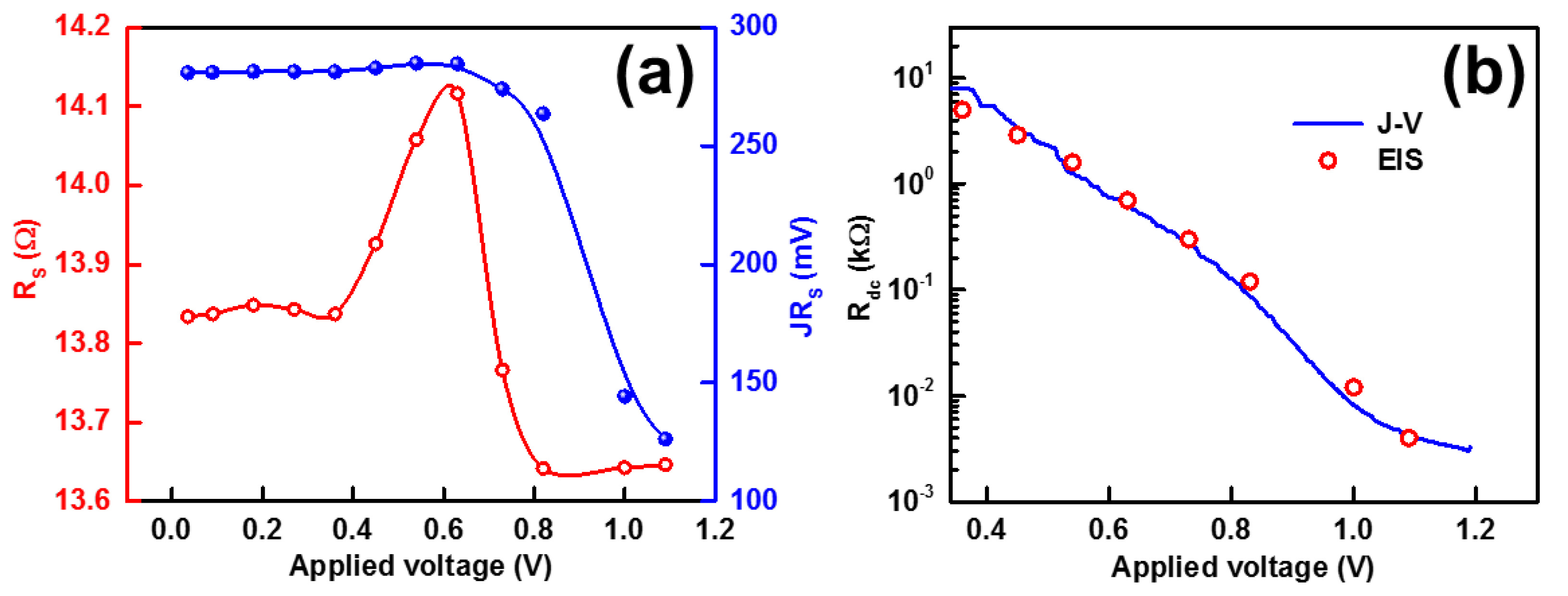
Figure 5.
(a) The capacitance of a PSC extracted from the low and high frequency Nyquist spectra as a function of applied bias and (b) the variation of the high frequency time constant as a function of applied bias for a PSC.
Figure 5.
(a) The capacitance of a PSC extracted from the low and high frequency Nyquist spectra as a function of applied bias and (b) the variation of the high frequency time constant as a function of applied bias for a PSC.

© 2017 by the authors. Licensee MDPI, Basel, Switzerland. This article is an open access article distributed under the terms and conditions of the Creative Commons Attribution (CC BY) license (http://creativecommons.org/licenses/by/4.0/).
Share and Cite
MDPI and ACS Style
Yadav, P.; Prochowicz, D.; Saliba, M.; Boix, P.P.; Zakeeruddin, S.M.; Grätzel, M. Interfacial Kinetics of Efficient Perovskite Solar Cells. Crystals 2017, 7, 252. https://doi.org/10.3390/cryst7080252
AMA Style
Yadav P, Prochowicz D, Saliba M, Boix PP, Zakeeruddin SM, Grätzel M. Interfacial Kinetics of Efficient Perovskite Solar Cells. Crystals. 2017; 7(8):252. https://doi.org/10.3390/cryst7080252
Chicago/Turabian StyleYadav, Pankaj, Daniel Prochowicz, Michael Saliba, Pablo P. Boix, Shaik M. Zakeeruddin, and Michael Grätzel. 2017. "Interfacial Kinetics of Efficient Perovskite Solar Cells" Crystals 7, no. 8: 252. https://doi.org/10.3390/cryst7080252
Note that from the first issue of 2016, this journal uses article numbers instead of page numbers. See further details here.