Evaluation of Thin Copper Wire and Lead-Free Solder Joint Strength by Pullout Tests and Wire Surface Observation


Graduate School of Natural Science and Technology, Okayama University, Okayama 700-8530, Japan
*
Author to whom correspondence should be addressed.
Crystals 2017, 7(8), 255; https://doi.org/10.3390/cryst7080255
Submission received: 13 July 2017
/
Revised: 13 August 2017
/
Accepted: 18 August 2017
/
Published: 20 August 2017
(This article belongs to the Special Issue Advance in Crystalline Thin Wires)
Abstract
:Copper wires have been attracting much attention for Large Scale Integration (LSI) bonding because of their excellent mechanical and electrical properties, in addition to their low material cost. The ends of these wires are usually joined to pads or through-holes on a printed circuit board, and lead-free soldering is one of the popular bonding methods. Since the deformation resistance of solder is lower than that of copper, especially in slow deformation due to creep, the strain tends to be increased in the solder and concentrated near the copper/solder joint interface. Thus, fracture frequently occurs at this interface and may influence the quality of the product. It is therefore important to evaluate the bonding strength of thin copper wire and lead-free solder. In this paper, pullout tests of thin copper wire from lead-free solder were carried out, and the pullout behavior of the wires was observed. The bonding strength was evaluated based on the actual bonded area on the copper wire surface. Finally, the strength of the thin copper wire/solder joint was summarized using the shear and tensile strengths of the copper/solder interface as well as the tensile strength of the copper wire.
1. Introduction
Gold wire is a very popular interconnection material in semiconductor packaging. However, alternative metals gradually come to be used for wiring to reduce the cost [1,2]. Copper is one such alternatives because of its higher electrical conductivity, higher stiffness, and low growth rate of intermetallics with aluminum. The mechanical properties and strength of thin copper wires have been investigated. For example, Yang et al. investigated the fatigue behavior of micro-sized pure copper wires and clarified the deformation mechanism in low- and high-cycle fatigue regimes [3,4]. Huang et al. investigated the mechanical properties and pull fracture mechanism of thin advanced copper wires and the effect of the EFO (electric flame-off) process was clarified based on the results of tensile tests and nano-indentations [5]. The authors also carried out tensile tests of thin wire of polycrystalline copper and measured the microscopic deformation on the surface using a digital holographic microscope (DHM). Inhomogeneous deformation was observed, and the surface roughness under relatively large load was well correlated with surface undulation under small load [6].
In addition to the strength of thin wires themselves, the accurate evaluation of bonding strength is very important to increase the reliability of electric packages. Kobayashi investigated the thermal stress that remained in copper wire after soldering and measured the strength of solder fillet against the pull of copper wire [7]. It was found that the thermal stress depended on the main shrinking directions of the copper wire and solder fillet. The logarithmic time to the pullout of the wire from the land under static load was roughly proportional to the height of the fillet. However, the plots were scattered along the relation and the slope depended on the tensile load and temperature. It is understood that the pullout strength cannot be evaluated accurately only from the size and shape of solder fillet. Since the through-hall components have a considerable margin of safety due to the relatively long and large solder/metal interface, very little research has been performed on this topic [7,8]. However, the pullout strength of thin wire from lead-free solder is still important considering the further miniaturization of products.
In this study, pullout tests of thin copper wire from lead-free solder were carried out, and the pullout behavior of wires was observed. The bonding strength was examined based on the actual bonded area between the wire and solder. Finally, the strength of the thin copper wire/solder joint was summarized using the shear and tensile strengths of the copper/solder interface as well as the tensile strength of the copper wire.
2. Experimental Procedures
2.1. Solder Joint Specimen
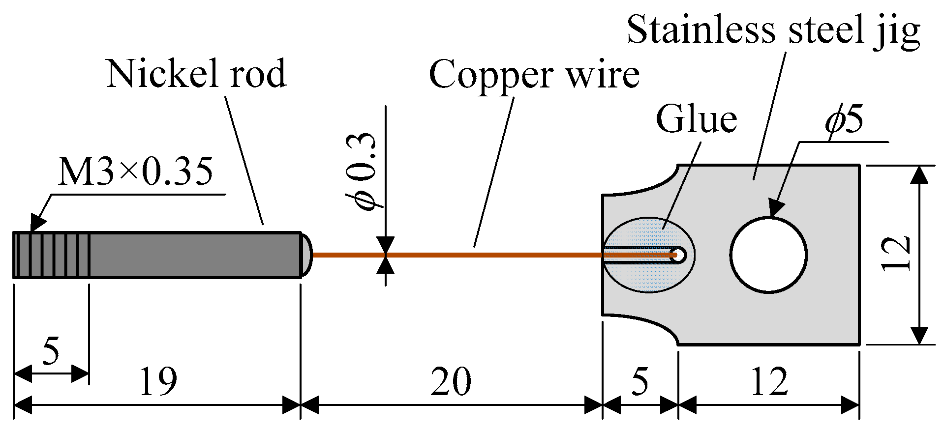
A solder joint specimen is shown in Figure 1. It is composed of a pure copper wire of purity 99.9% with a diameter of 0.3 mm, a nickel rod, and a stainless-steel jig. The bonding strength between the copper wire and solder was evaluated by the pullout tests of the specimens. The specimen was made by the following process:
- One end of the copper wire was mechanically polished using emery papers #800 and #1200 and an ultrasonic cleaning was performed by isopropanol.
- The other (unpolished) end of the copper wire was glued to the stainless-steel jig by cyanoacrylate-based instantaneous adhesive, and held together for more than one day to ensure complete hardening.
- A small piece of lead-free solder was cut and heated at the tip of a soldering iron to melt it into a spheroidal shape. Lead-free solder HS-304 (Sn-3Ag-0.5Cu) manufactured by Hozan tool industrial Co., Ltd., Osaka, Japan was used.
- The solder ball was put on the upper surface of the nickel rod standing in the vertical direction, and was heated on the hot plate. Soldering flux RM-5 manufactured by Nihon Superior Co., Ltd., Suita, Japan, was glued to the upper surface of the nickel rod before the heating.
- When the melting of the solder was confirmed, one end of the copper wire opposite to the jig side was inserted into the melted solder, and naturally cooled to room temperature for about an hour.
In the present experiments, the side surface of copper wire was used as received and only the bottom surface was mechanically polished to make it flat. Since additional experiments using copper wire with a mechanically polished side surface did not show significant difference, its effect on the bonding strength seems to be small.
2.2. Pullout Test
Pullout tests were carried out using a table-top type universal tester AGS-J manufactured by Shimadzu corporation, Kyoto, Japan. The stainless-steel jig and nickel rod of the specimen were chucked and the tensile displacement rate was controlled to be 2.0 mm/min (fast) or 0.5 mm/min (slow). The specimens for fast pullout tests are called “SC-2-i (I = 1 to 11)” and those for slow pullout tests are called “SC-0.5-i (I = 1 to 11)”, respectively. Eleven specimens were prepared for each of the fast and slow pullout tests. When either the pullout or fracture of copper wire was confirmed visually, the test was terminated and the surface of the copper wire was observed. Three specimens out of 11 were failed due to the fracture (or rapture) of the copper wire in the fast pullout tests, and five specimens out of 11 were failed due to the fracture of the copper wire in the slow pullout tests.
2.3. Apparent Height of Solder Joint and Actual Bond Length
For the specimens failed by the pullout of the copper wire, the bonded area was evaluated in two different methods. One is the apparent height of the solder joint, which was defined as the distance between the top of the solder joint and the top surface of the nickel rod, as shown in Figure 2. This measurement was taken before each pullout test. The other method is the actual bond length of the solder joint, which was evaluated after the test by the following procedure.
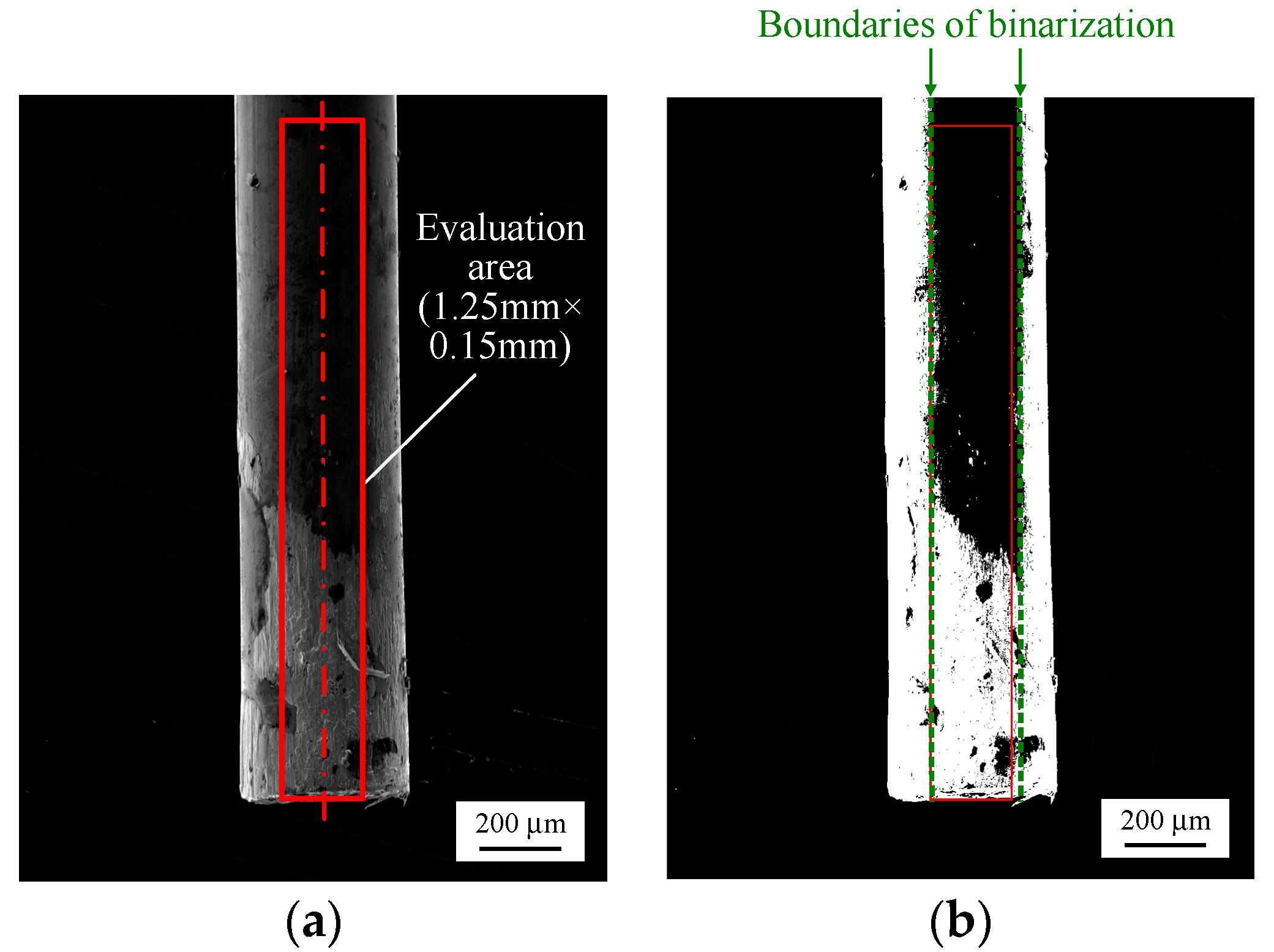
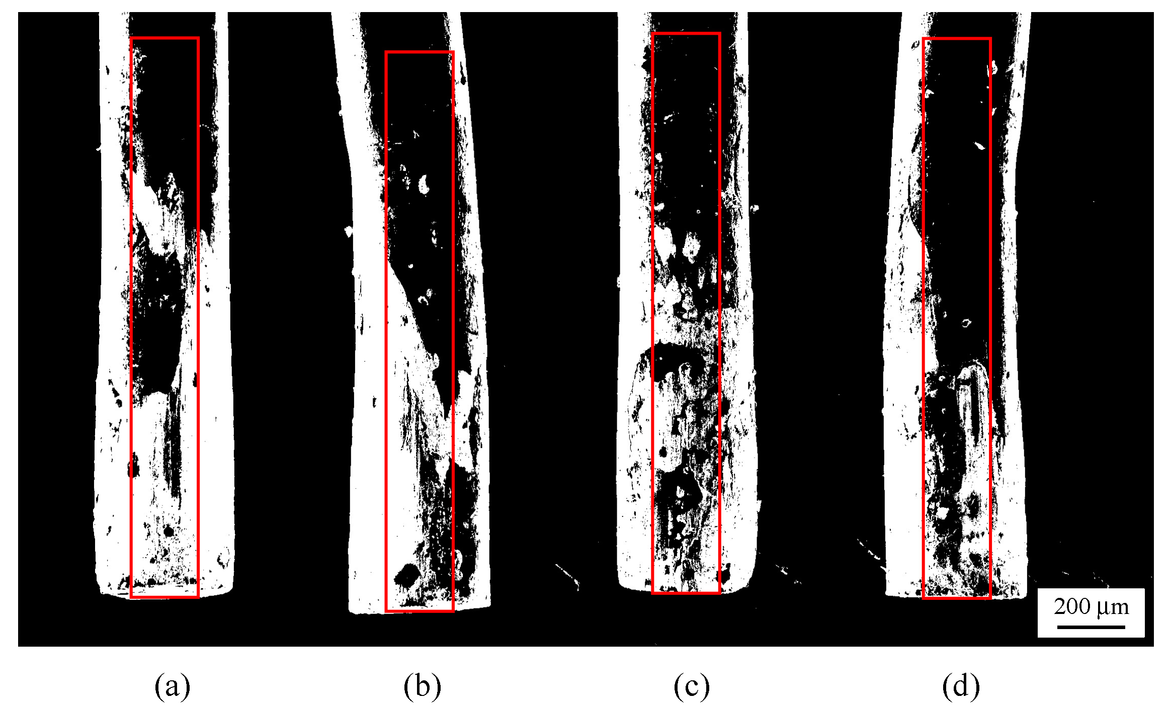
- The observation of the copper wire surface was carried out in four orthogonal directions by a scanning electron microscope (SEM, Hitachi, S-3500N, Tokyo, Japan). An evaluation area of 1.25 mm × 0.15 mm (1100 × 132 pixels), shown by a red rectangle in Figure 3a, was set on the surface of the copper wire. Its location was determined so that the center line and the bottom side coincided with those of the copper wire, respectively. The observation of the copper wire surface was also performed by the optical microscope, and it was confirmed that the brighter areas observed by SEM corresponded to the remaining silver solder.
- As seen in Figure 3a, the actual bonded area is brighter than the other area. On the other hand, when focusing on the upper portion of the copper wire where there is no bonded area, the peripheral area along the edge of copper wire is brighter than the central area. Considering these characteristics of the SEM image, the threshold of binarization was determined as follows. Two parallel green broken lines in Figure 3b show the boundaries of binarization at a certain threshold. The boundaries move to the right and left according to the level of threshold. In this study, the binarization threshold was determined so that two parallel lines are situated on or outside the evaluation area. Taking the threshold value, only the bonded area becomes white in the evaluation area.
- The number of white pixels corresponding to the bonded area was counted and converted to the actual area in mm2. The actual bond length was evaluated by dividing the bonded area by the width of the evaluation area, 0.15 mm, which represents the average height of the bonded area.
- The above steps 1 to 3 were repeated in four orthogonal directions and the values were averaged.
3. Experimental Results
3.1. Load-Displacement Diagram
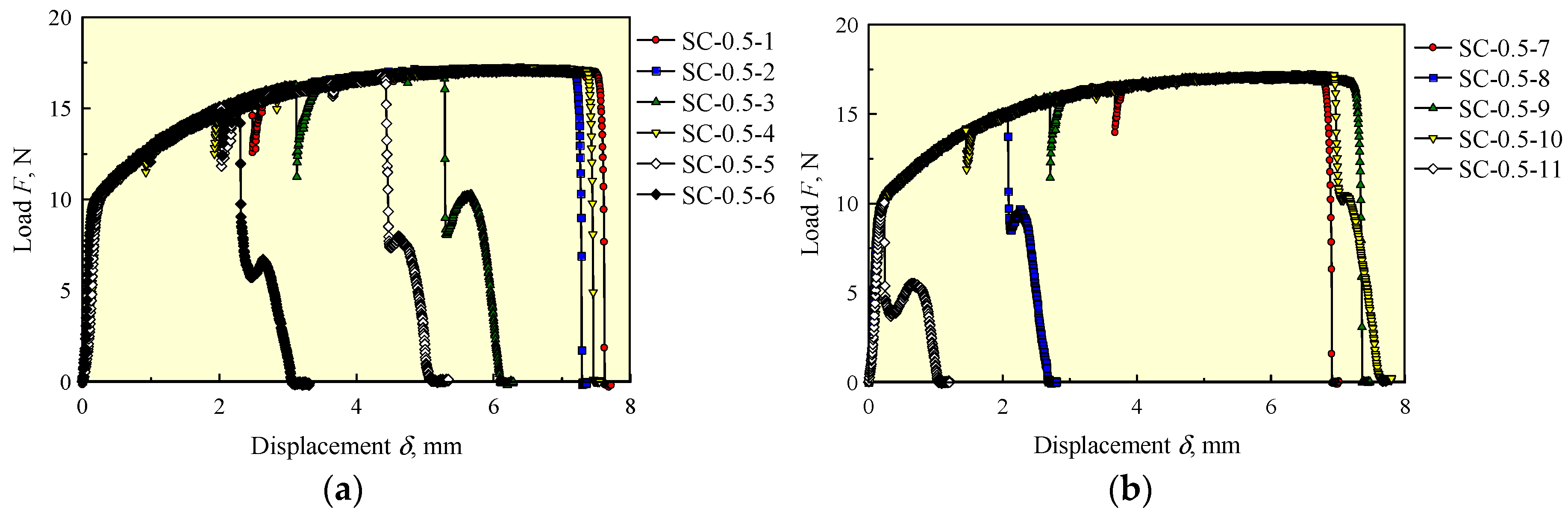
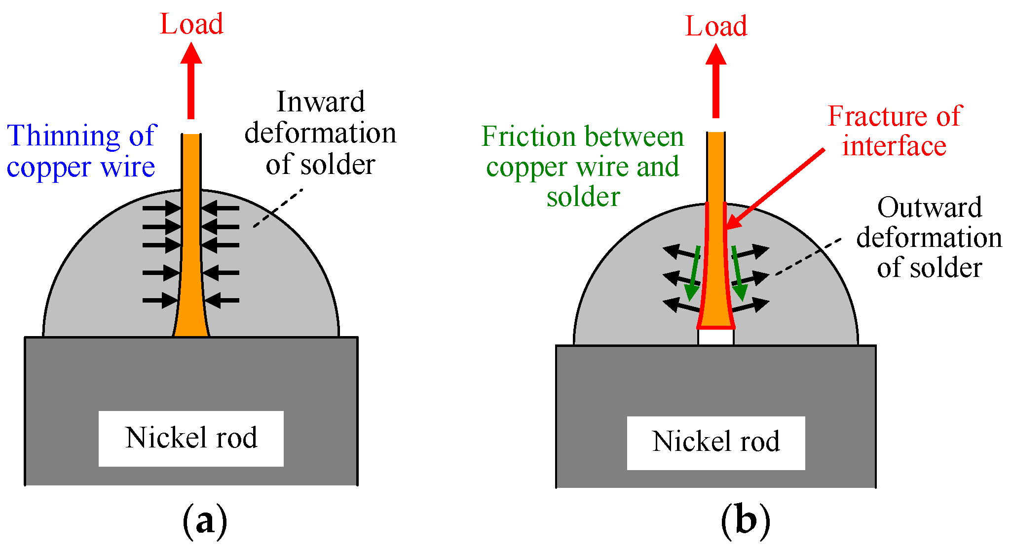
Load-displacement diagrams of fast pullout tests (SC-2 series) are shown in Figure 4, and those of slow pullout tests (SC-0.5 series) are shown in Figure 5. Their maximum load Fmax varied depending on the specimen, but all of the curves are very similar until the maximum load. These characteristics are found both in fast and slow pullout tests. Considering that these curves coincide with the load-displacement diagram obtained by the tensile tests of the copper wire, the curves show the elastic and plastic property of the copper wires. Small spikes of load decrease are found during the loading process in some specimens. These were caused by the partial fracture of glue on the stainless-steel jig, although their effect on the pullout strength is considered to be very small. Another interesting point is the re-increase of load during the unloading process. Most specimens that failed by pullout of the copper wire showed the load re-increase. It is anticipated that the load re-increase was caused by the friction between the surface of the copper wire covered with the thin solder film and the inner surface of the solder during the pullout process. The opening deformation of solder near the copper wire seems to have contributed to the load re-increase, which is conceivable from the larger diameter of the copper wire at the bottom, as shown in Figure 6 and Figure 7.
3.2. Surface of the Copper Wire
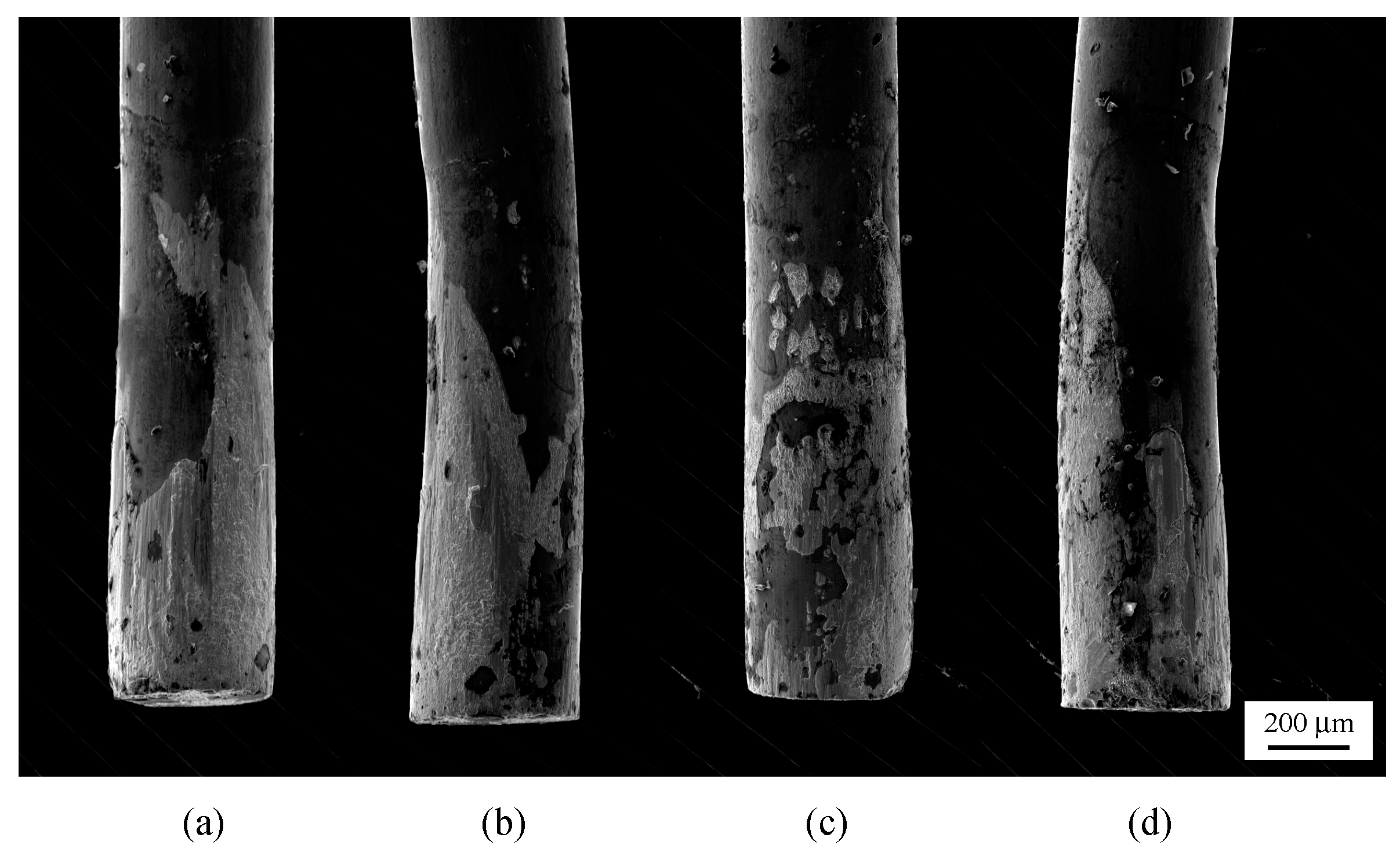
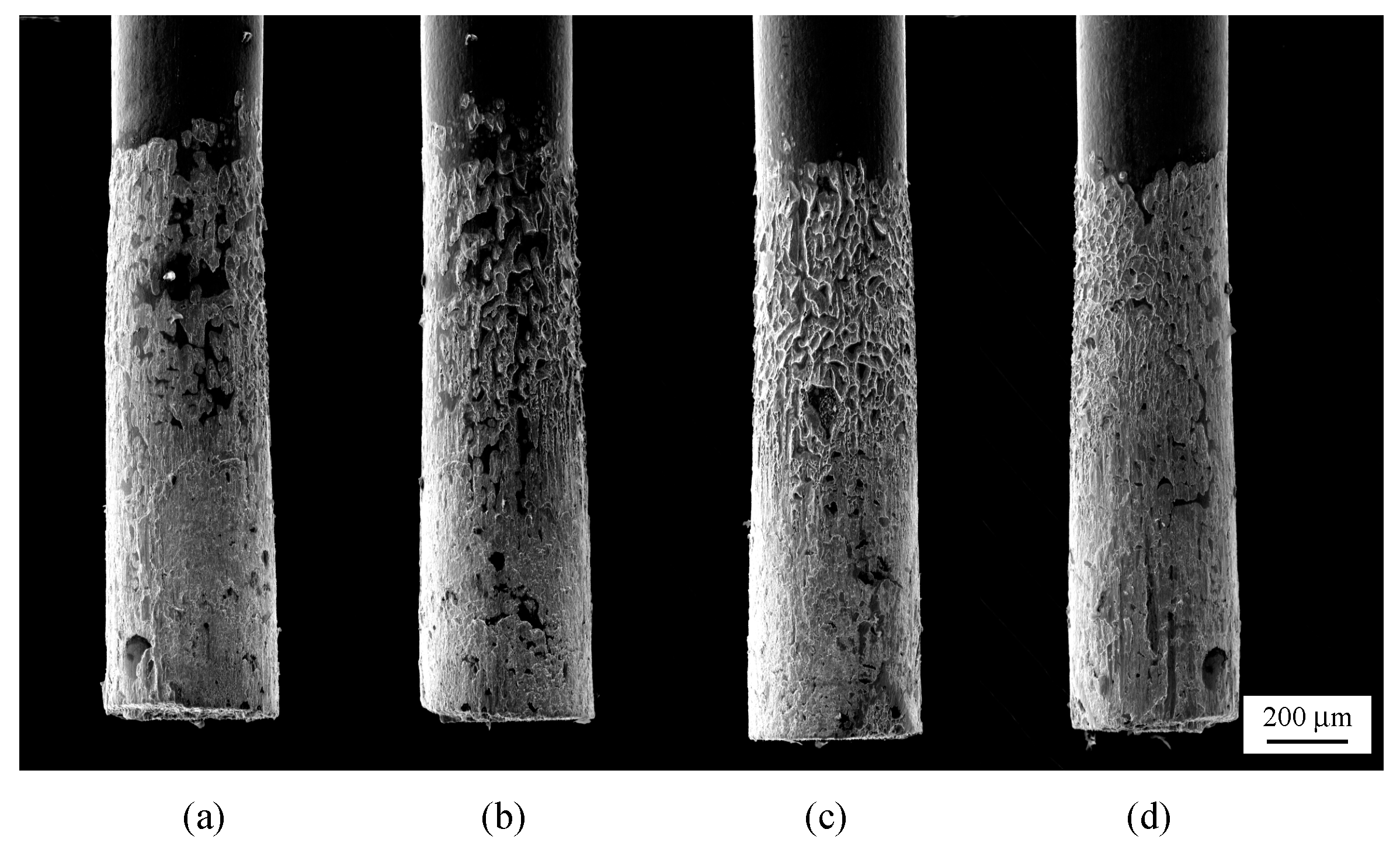
Examples of the copper wire surface observed by SEM after the fast and slow pullout tests are shown in Figure 6 and Figure 7, respectively. The bright gray parts are the remaining solder films which were firmly bonded to the surface of the copper wire. The slightly smaller diameter of the copper wire near the top of the bonded area shows that the deformation of the copper wire was relatively large near the top of the solder. The average difference in the copper wire diameter between the bottom and 1 mm above the bottom was about 7% after the pullout tests. The difference contains the thickness of the thin solder film that remained on the side surface of the wire. A main cause of this difference is considered to be the slightly different constraint of the copper wire deformation by the surrounding solder, as schematically shown in Figure 8. The suppression of the copper wire’s shrink in a radial direction by the solder may have controlled the longitudinal deformation of the copper wire. It is also considered that the difference in the diameter of the copper wire became resistant to the pullout process, as shown in Figure 8b. Various morphologies were observed, such as the smooth thin solder films shown in Figure 6 and the relatively thick films with mottled regions like fish scales shown in Figure 7. The complex shape of the bonded area indicates a need for image processing to evaluate the actual bonded area. No significant difference was observed between the surface of the fast pullout specimens and that of the slow pullout specimens.
3.3. Relationship between Maximum Load and Bond Length of Solder Joint
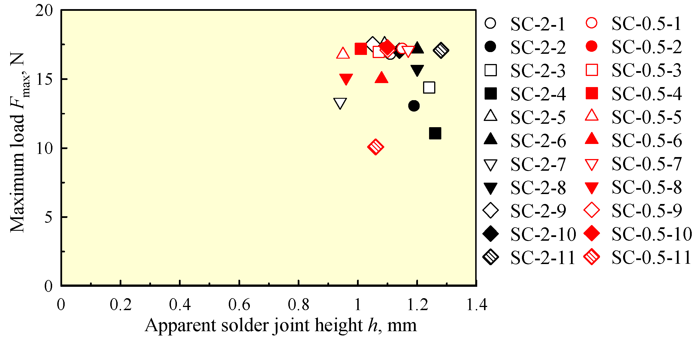
The relationship between the maximum load, Fmax, and apparent height of the solder joint, h, is shown in Figure 10. The plots are scattered for fast and slow pullout specimens and no clear correlation is observed between Fmax and h. The scatter is caused by the complex shape of the actual bonded area, which cannot be estimated from the appearance of the solder joint.
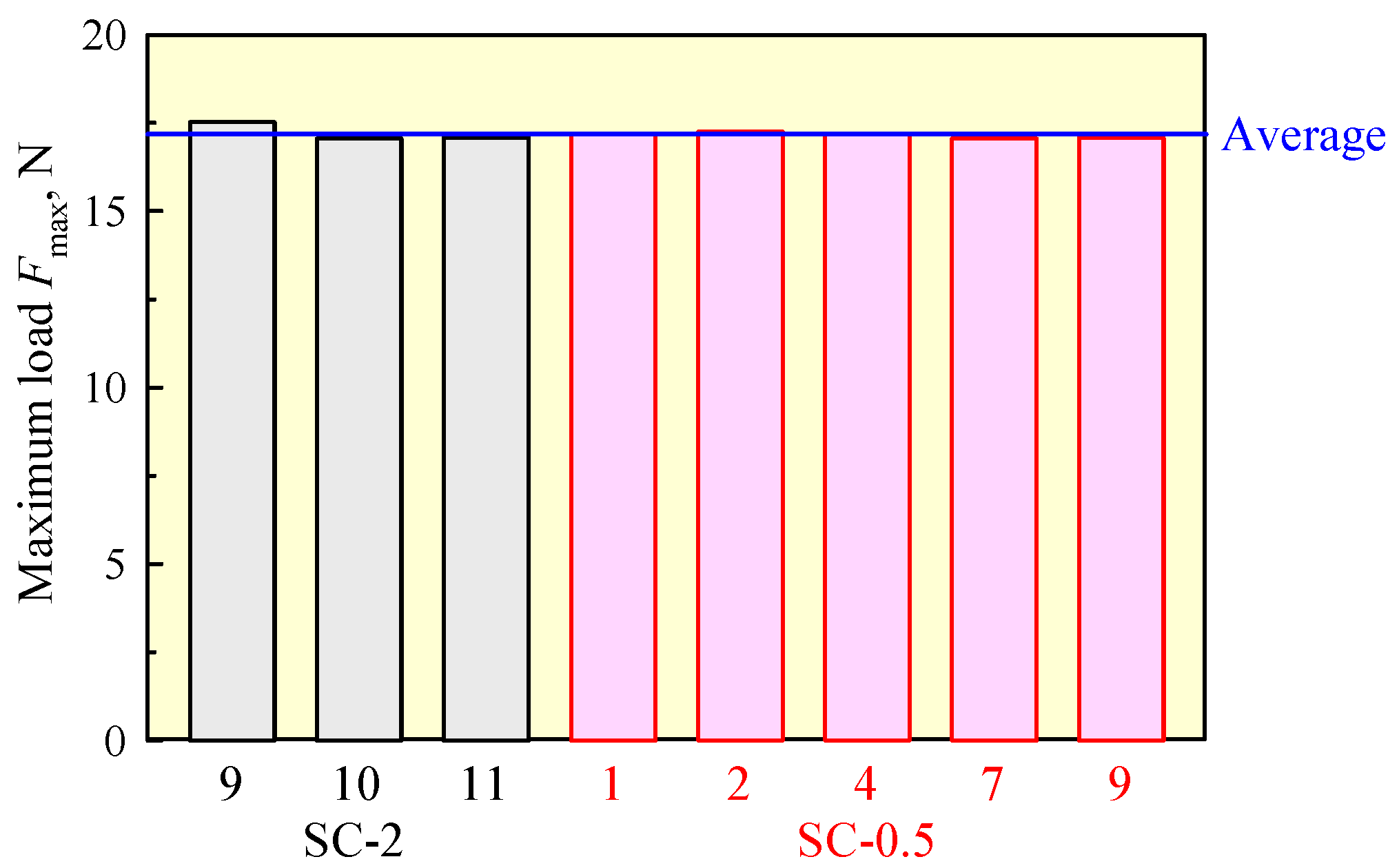
The maximum load for eight specimens failed by the fracture of the copper wire is shown in Figure 11. All the specimens showed almost the same value, and the average load was 17.19 N. The tensile strength of copper wires used in the present tests is stable. The fact that eight out of 22 specimens failed due to the fracture of the copper wire indicates that the pullout strength of the copper wire/solder joint and the tensile strength of the copper wire are close to each other.
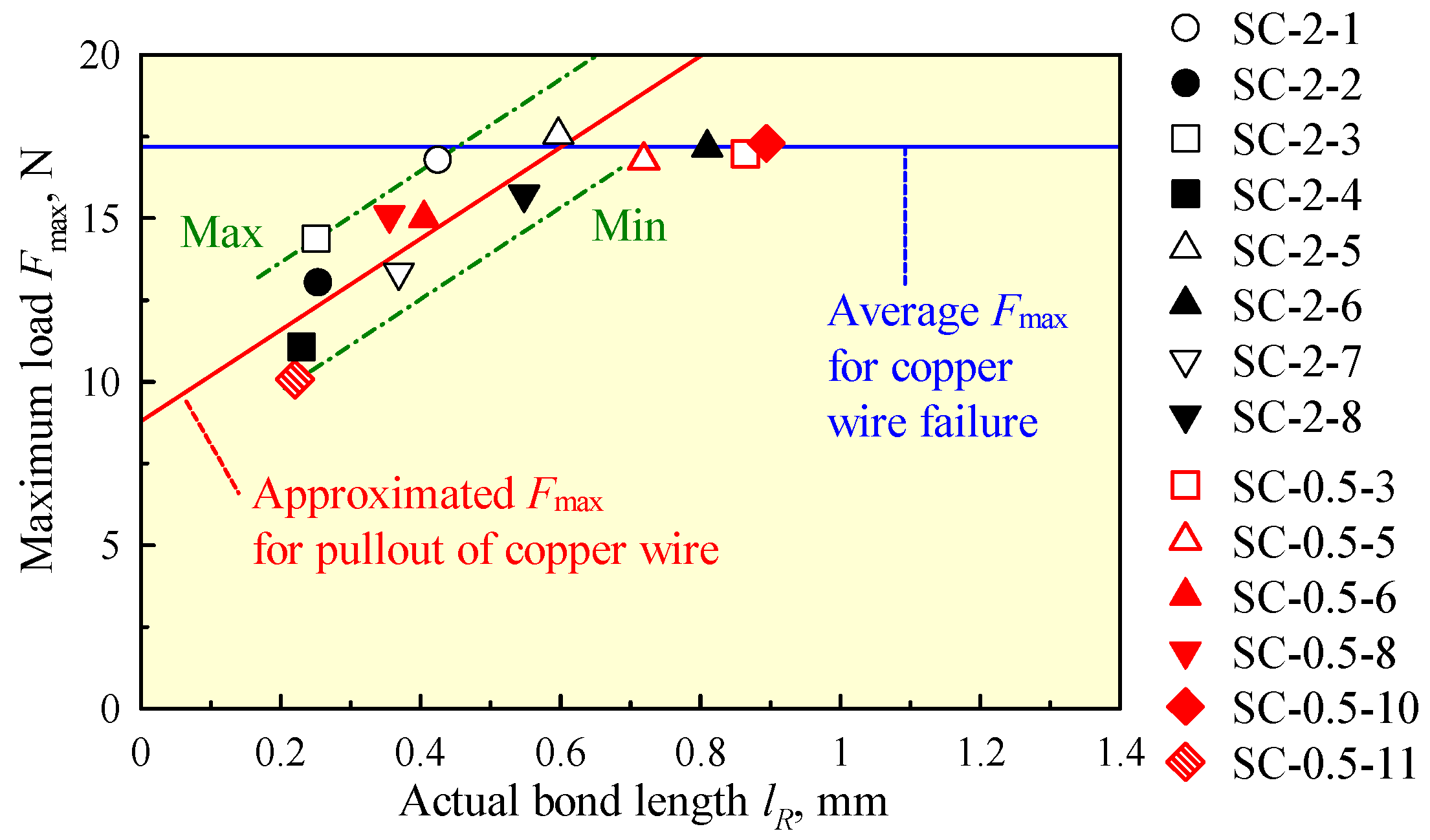
Figure 12 shows the relationship between the maximum load, Fmax, and the actual bond length, lR, for the specimens failed by the pullout of the copper wire. The blue horizontal line shows the average of the maximum load for the specimens failed by the copper wire fracture, as was shown in Figure 11. The red straight line is an approximated line which was determined by the least-square method for the results, except for six plots within a 5% range of the blue average load line. The reason for the exception follows. Since the interface strength of the copper wire/solder and the tensile strength of the copper wire are considered to be very close to each other, they might have failed by the fracture of copper wire. In addition, their positions in the Fmax-lR relationship strongly affect the determination of the approximated line. Although the plots are scattered, all of the plots are distributed near the red and blue lines. This result suggests that the maximum load according to the pullout tests is determined by the actual bonded length and the tensile strength of the copper wire.
4. Evaluation of Tensile and Shear Strengths of the Copper/Solder Interface
Assuming that the interface of the copper wire and solder is composed of the side and bottom surfaces of the cylindrical end of the copper wire, the maximum load, Fmax, is given by the sum of the tensile and shear strengths of copper/solder interface as follows:
where σf and τf are the tensile and shear interface strengths, d is the diameter of the copper wire, and pR and lR are the fraction of the actual bonded area to the total area on the bottom surface and the actual bond length evaluated using the binary image, respectively. Here, the relationship between Fmax and lR can be expressed by:
as was shown in Figure 12, where F0 (= 8.79 N) and b (= 13.96 N/mm) are determined from the intercept of Fmax-axis and the slope of the approximated line, respectively. Comparing Equations (1) and (2), we can assume that pR = 1, σf = 124.4 MPa, and τf = 14.8 MPa are obtained. It was confirmed by SEM observation that the actual bonded area on the bottom surface of the copper wire is about 1, independent of the specimen. The value of the tensile interface strength is a little high in comparison with the other results (σf = 50 to 90 MPa) obtained for similar lead-free solders and copper [9,10], and that of the shear interface strength is lower than the previous result (τf = 40 MPa) [11]. The constraint of plastic deformation at the bottom surface of the copper wire [12,13], the size and shape of the specimens, and the data dispersion (which will be described below) may be the reason for these differences.
In order to investigate the effect of data dispersion on the evaluation of the interface strength, two parallel lines passing through the points most distant from the straight line given by Equation (2) are considered, as shown in Figure 12. The tensile interface strengths evaluated by these lines are 153.3 MPa and 99.0 MPa, respectively. Since the two lines have the same inclination, the shear interface strength does not change. If an accurate value of the interface strength or its distribution is required, a large number of pullout tests are necessary, and the microstructures of the solder and copper wire as well as their change near the copper/solder interface should be investigated [14,15].
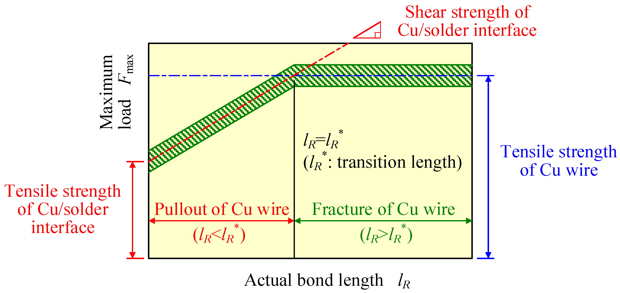
Finally, the strength of the copper wire/solder joint is schematically shown in Figure 13. A red chain-line shows the shear strength of the copper/solder interface. The strength increases with the actual bond length, lR, and its intercept of Fmax-axis becomes the tensile strength of the copper/solder interface on the bottom surface of the copper wire, because no bonded area exists on the side surface of the copper wire when lR = 0. A blue-chain line shows the tensile strength of the copper wire, which is obtained by the tensile test of the copper wire without the solder joint. Here, the transition length, lR*, is defined as the intersection of shear and tensile strength lines. When the actual bond length of the copper wire/solder joint is less than lR*, the interface strength is governed by the shear strength of the copper/solder interface. On the other hand, when lR is larger than lR*, the joint is strong enough and the copper wire becomes fractured at the tensile strength of the copper wire before the pullout of the copper wire. This relationship is useful for the determination of the geometry of the copper wire and solder in an actual electric package.
5. Conclusions
Pullout tests were carried out using a thin copper wire/solder joint. The bonding strength of the copper/solder interface was evaluated. Not only the apparent height of the solder joint but also the actual bond length were evaluated based on the observation of the copper wire surface after the pullout test. The maximum load in the pullout test was not correlated with the apparent height of the solder joint, but it was well correlated with the actual bond length of the solder joint. Based on these results, the strength of the solder joint was summarized using the shear and tensile strengths of the copper/solder interface as well as the tensile strength of the copper wire. Finally, the transition length was proposed, by which the fracture type of the copper wire/solder joint (i.e., pullout or tensile fracture of copper wire) can be predicted.
Author Contributions
Naoya Tada conceived and designed the experiments; Naoya Tada and Takuhiro Tanaka performed the experiments; Takeshi Uemori and Toshiya Nakata analyzed the data; Naoya Tada wrote the paper.
Conflicts of Interest
The authors declare no conflict of interest.
References
- Breach, C.D. What is the Future of Bonding Wire? Will Copper Entirely Replace Gold? Gold Bull. 2010, 43, 150–168. [Google Scholar] [CrossRef]
- Gan, C.L.; Hashim, U. Evolution of Bonding Wires Used in Semiconductor Electronics: Perspective over 25 Years. J. Mater. Sci. Mater. Electron. 2015, 26, 4412–4424. [Google Scholar] [CrossRef]
- Yang, B.; Motz, C.; Grosinger, W.; Dehm, G. Stress-Controlled Fatigue Behavior of Micro-Sized Polycrystalline Copper Wires. Mater. Sci. Eng. 2009, 515, 71–78. [Google Scholar] [CrossRef]
- Yang, B.; Motz, C.; Grosinger, W.; Dehm, G. Cyclic Loading Behavior of Micro-Sized Polycrystalline Copper Wires. Proced. Eng. 2010, 2, 925–930. [Google Scholar] [CrossRef]
- Huang, I.-T.; Hung, F.-Y.; Lui, T.-S.; Chen, L.-H.; Hsueh, H.-W. A Study on the Tensile Fracture Mechanism of 15 μm Copper Wire after EFO Process. Microelectron. Reliab. 2011, 51, 25–29. [Google Scholar] [CrossRef]
- Tada, N.; Matsukawa, Y.; Uemori, T.; Nakata, T. Microscopic Deformation of Polycrystalline Pure Copper Wire during Tension. In Proceedings of the 10th International Microsystems, Packaging, Assembly and Circuits Technology Conference, Taipei, Taiwan, 21–23 October 2015; pp. 420–423. [Google Scholar]
- Kobayashi, M. Reliability of Soldered Connections in Single Ended Circuit Components. Weld. Res. Suppl. 1975, 363-s–369-s. [Google Scholar]
- Susan, D.F.; Kilgo, A.C.; Vianco, P.T.; Neilsen, M.K. Thermal Fatigue and Failure Analysis of Cu-Plated Through Hole Solder Joints. Microsc. Microanal. 2009, 15, 26–27. [Google Scholar] [CrossRef]
- Zeng, G.; Xue, S.; Zhang, L.; Gao, L.; Dai, W.; Luo, J. A Review on the Interfacial Intermetallic Compounds between Sn-Ag-Cu Based Solders and Substrates. J. Mater. Sci. Mater. Electron. 2010, 21, 421–440. [Google Scholar] [CrossRef]
- An, T.; Qin, F. Effects of Intermetallic Compound Microstructure on the Tensile Behavior of Sn3.0Ag0.5Cu/Cu Solder Joint under Various Strain Rates. Microelectron. Reliab. 2014, 54, 932–938. [Google Scholar] [CrossRef]
- Anderson, I.E.; Harringa, J.L. Elevated Temperature Aging of Solder Joints Based on Sn-Ag-Cu: Effects on Joint Micsostructure and Shear Strength. J. Electron. Mater. 2004, 33, 1485–1496. [Google Scholar] [CrossRef]
- Cugnoni, J.; Botsis, J.; Sivasubramaniam, V.; Janczak-Rusch, J. Experimental and Numerical Studies on Size and Constraining Effects in Lead-Free Solder Joints. Fatigue Fract. Eng. Mater. Struct. 2007, 30, 387–399. [Google Scholar] [CrossRef]
- Zimprich, P.; Saeed, U.; Weiss, B.; Ipser, H. Constraining Effects of Lead-Free Solder Joints During Stress Relaxation. J. Electron. Mater. 2008, 38, 392–399. [Google Scholar] [CrossRef]
- Fujiwara, S.; Dauskardt, R.H. Interface Structure of Cu Wire Bonding on Cu Substrate with Sn Plating. Mater. Trans. 2012, 53, 2091–2096. [Google Scholar] [CrossRef]
- Anderson, I.E.; Cook, B.A.; Harringa, J.L.; Terpstra, R.L. Sn-Ag-Cu Solders and Solder Joints: Alloy Development, Microstructure, and Properties. JOM J. Miner. Met. Mater. Soc. 2002, 54, 26–29. [Google Scholar] [CrossRef]
Figure 1.
Shape and size of solder joint specimen.

Figure 2.
Solder joint before pullout test and its apparent height.
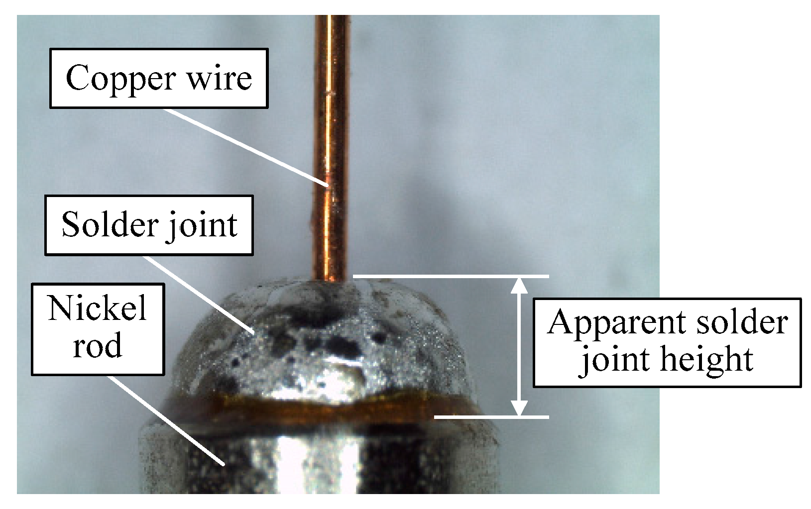
Figure 3.
Evaluation of bonded area on the surface: (a) Evaluation area; (b) Binarization for boundary determination.
Figure 3.
Evaluation of bonded area on the surface: (a) Evaluation area; (b) Binarization for boundary determination.

Figure 4.
Load-displacement diagrams: (a) Specimens SC-2-1 to 6; (b) Specimens SC-2-7 to 11.
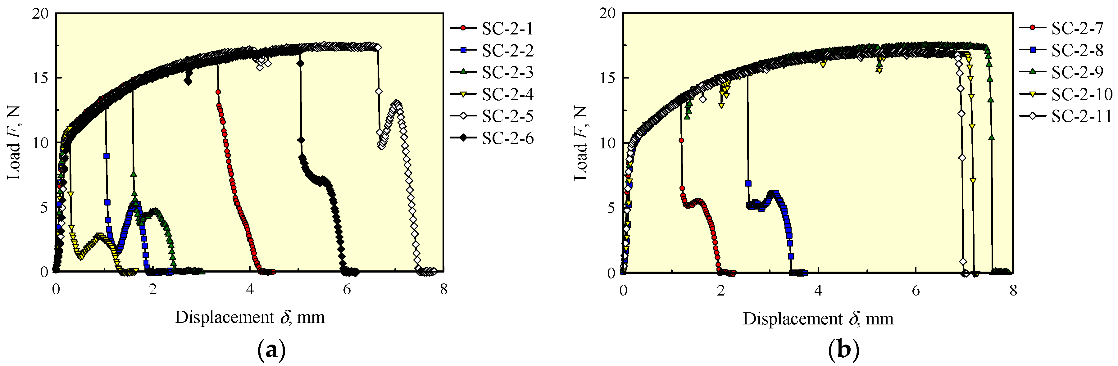
Figure 5.
Load-displacement diagrams: (a) Specimens SC-0.5-1 to 6; (b) Specimens SC-0.5-7 to 11.

Figure 6.
Surface of copper wire (SC-2-1) after pullout test taken in four orthogonal directions: (a) 0 degrees; (b) 90 degrees; (c) 180 degrees; (d) 270 degrees.
Figure 6.
Surface of copper wire (SC-2-1) after pullout test taken in four orthogonal directions: (a) 0 degrees; (b) 90 degrees; (c) 180 degrees; (d) 270 degrees.

Figure 7.
Surface of copper wire (SC-0.5-3) after pullout test taken in four orthogonal directions: (a) 0 degrees; (b) 90 degrees; (c) 180 degrees; (d) 270 degrees.
Figure 7.
Surface of copper wire (SC-0.5-3) after pullout test taken in four orthogonal directions: (a) 0 degrees; (b) 90 degrees; (c) 180 degrees; (d) 270 degrees.

Figure 8.
Deformation of copper wire and solder in pullout test: (a) During load increasing; (b) During unloading after the maximum load.
Figure 8.
Deformation of copper wire and solder in pullout test: (a) During load increasing; (b) During unloading after the maximum load.

Figure 9.
Binary image of copper wire (SC-2-1) surface and the evaluation area (red rectangle): (a) 0 degrees; (b) 90 degrees; (c) 180 degrees; (d) 270 degrees.
Figure 9.
Binary image of copper wire (SC-2-1) surface and the evaluation area (red rectangle): (a) 0 degrees; (b) 90 degrees; (c) 180 degrees; (d) 270 degrees.

Figure 10.
Relationship between the maximum load, Fmax, and apparent solder joint height, h, for all fast and slow pullout specimens.
Figure 10.
Relationship between the maximum load, Fmax, and apparent solder joint height, h, for all fast and slow pullout specimens.

Figure 11.
The maximum load, Fmax, for the eight specimens failed by fracture of copper wire.

Figure 12.
Relationship between the maximum load, Fmax, and the actual bond length, lR, for specimens failed by pullout of copper wire.
Figure 12.
Relationship between the maximum load, Fmax, and the actual bond length, lR, for specimens failed by pullout of copper wire.

Figure 13.
Tensile and shear strengths of copper/solder interface and tensile strength of copper wire in the relationship between the maximum load and actual bond length.
Figure 13.
Tensile and shear strengths of copper/solder interface and tensile strength of copper wire in the relationship between the maximum load and actual bond length.

© 2017 by the authors. Licensee MDPI, Basel, Switzerland. This article is an open access article distributed under the terms and conditions of the Creative Commons Attribution (CC BY) license (http://creativecommons.org/licenses/by/4.0/).
Share and Cite
MDPI and ACS Style
Tada, N.; Tanaka, T.; Uemori, T.; Nakata, T. Evaluation of Thin Copper Wire and Lead-Free Solder Joint Strength by Pullout Tests and Wire Surface Observation. Crystals 2017, 7, 255. https://doi.org/10.3390/cryst7080255
AMA Style
Tada N, Tanaka T, Uemori T, Nakata T. Evaluation of Thin Copper Wire and Lead-Free Solder Joint Strength by Pullout Tests and Wire Surface Observation. Crystals. 2017; 7(8):255. https://doi.org/10.3390/cryst7080255
Chicago/Turabian StyleTada, Naoya, Takuhiro Tanaka, Takeshi Uemori, and Toshiya Nakata. 2017. "Evaluation of Thin Copper Wire and Lead-Free Solder Joint Strength by Pullout Tests and Wire Surface Observation" Crystals 7, no. 8: 255. https://doi.org/10.3390/cryst7080255
Note that from the first issue of 2016, this journal uses article numbers instead of page numbers. See further details here.