Van der Waals Heterostructure Based Field Effect Transistor Application

State Key Laboratory of ASIC and System, School of Microelectronics, Fudan University, Shanghai 200433, China
*
Author to whom correspondence should be addressed.
†
These authors contributed equally to this work.
Crystals 2018, 8(1), 8; https://doi.org/10.3390/cryst8010008
Submission received: 16 November 2017
/
Revised: 18 December 2017
/
Accepted: 20 December 2017
/
Published: 26 December 2017
(This article belongs to the Special Issue Integration of 2D Materials for Electronics Applications)
Abstract
:Van der Waals heterostructure is formed by two-dimensional materials, which applications have become hot topics and received intensive exploration for fabricating without lattice mismatch. With the sustained decrease in dimensions of field effect transistors, van der Waals heterostructure plays an important role in improving the performance of devices because of its prominent electronic and optoelectronic behavior. In this review, we discuss the process of assembling van der Waals heterostructures and thoroughly illustrate the applications based on van der Waals heterostructures. We also present recent innovation in field effect transistors and van der Waals stacks, and offer an outlook of the development in improving the performance of devices based on van der Waals heterostructures.
1. Introduction
In the past few decades, graphene, which exhibits extraordinary electronic and optoelectronic properties in exploring low-dimensional materials, has become the most advanced research in the field of two-dimensional layered material (2DLM) science, solid-state physics and engineering [1,2,3]. Because graphene originally has excellent parameters, such as mechanical stiffness, strength and elasticity, very high electrical and thermal conductivity, graphene-based transistor preforms better than conventional Si-based transistors [1] in fabricating high-frequency transistors with the possible cut-off frequency fT = 1THz at a channel length of about 100 nm [4] and photodetectors with a wide spectral from ultraviolet to infrared [1]. Therefore, the discovery of graphene creates a new generation of electronic devices with atomically thin geometry and unprecedented combination of speed and flexibility. Except for the advantages and merits of graphene-based transistor mentioned above, there are some shortcomings, such as the unique zero bandgap, hindering the graphene’s application in electronic industry [3]. To overcome the defect brought by graphene device, this extensive library of 2DLMs, such as graphene, phosphorene, hexagonal boron nitride and transition metal dichalcogenide mentioned in this article with selected properties opens up the possibility of heterogeneous integration at the atomic scale, creating novel hybrid structures that display totally new physics and enable unique functionality [5]. Because 2DLMs have various bandgap, the different material shows different property. For example, black phosphorus shows the characteristic of conductor; molybdenum disulfide (MoS2) and tungsten selenide (WSe2) are semiconductors; and boron nitride (BN) performs as insulator. 2DLMs with various properties make it possible to form special combination of heterogeneous integration at atom scale, such as van der Waals heterostructures (vdWHs).
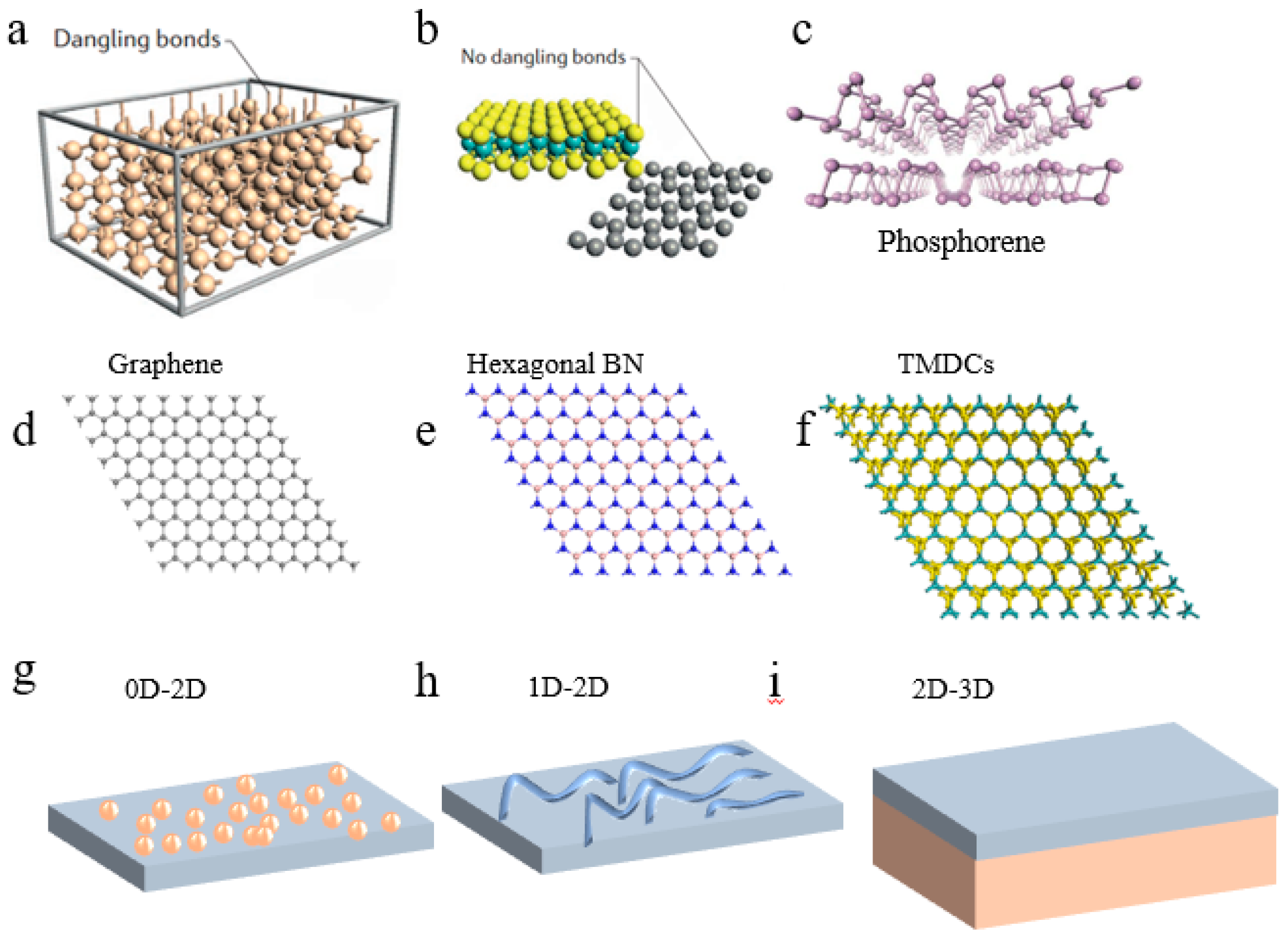
In general, heterostructures formed by 2DLM monolayers are assembled by covalent bond force within layers and stacked together by van der Waals force between layers. Thus, there is no free dangling bond between 2DLM layers. In contrast to typical nanostructures persecuted by dangling bond and trap state on the surfaces [6], monolayer are free of these disadvantages (Figure 1a,b) and exhibit extraordinary electronic and optoelectronic properties. Additionally, without free dangling bonds, the interface between neighbor 2DLM layers are assembled by van der Waals forces, which is much weaker than chemical bond force. Therefore, the van der Waals heterostructure can be easily isolated by exfoliation with the help of taps [7]. Although some highly disparate materials have a great lattice mismatch in creating heterostructure, those can be assembled together by van der Waals force. This allows diverse 2DLMs to construct various van der Waals heterostructures (vdWHs) with completely novel properties and functions.
The early study in vdWHs focus on the combination of 2DLMs with 0D (for example, plasmonic nanoparticles and quantum dots) and 1D (for example, nanowires and nanoribbons) nanostructures [9,10,11,12]. These novel 0D–2D (Figure 1f) and 1D–2D (Figure 1g) vdWHs structures have fabricated many highly performed devices, such as photodetectors with highly optical response [10] and transistors with high speed and flexibility [12]. In recent years, most efforts have been taken to form 2D–2D integration vdWHs by vertically stacking various 2DLMs; for example, Dean fabricated a graphene–BN heterostructure transistor which Hall mobility reached ~25,000 cm2·V−1·s−1 at high density [13], and Withers stacked metallic graphene, insulating hexagonal boron nitride and various semiconducting monolayers into complex but carefully designed sequences, which exhibited an extrinsic quantum efficiency of nearly 10% and the emission can be tuned over a wide range of frequencies by appropriately choosing and combining 2D semiconductors [14]. 2D–2D vdWHs with diverse 2DLMs make it possible to accurately control and modulate the transport of charge carriers, excitons and photons within the atomic surface, and greatly promote the new generation of unique devices. Apart from 2D–2D vdWHs, 2DLMs can also be integrated with 3D bulk materials to form 2D–3D structures [8,15] (Figure 1f–h), which attract some interest. Hot electron transistors based on 2D–3D heterojunctions have been reported [16]. Gate tunable p-n junctions based on 2D–3D heterojunctions have been reported [17,18]. Heterojunction formed with MoS2 and p type Ge can fabricate high performance tunneling field transistor [18].
Recently, most vdWHs are formed by mechanically stacking different monolayers together. Although this method allows great flexibility, it is slow and inconvenient. Thus, some simple and high-quality techniques are being developed, for example, large-area 2DLMs grown by chemical vapor deposition (CVD) and direct growth of heterostructure by CVD or physical epitaxy, which improves the growth quality of monolayers and the properties of heterostructure exhibited [19,20,21].
In this review, we mainly concentrate on the integration, properties, application and technology of vdWHs. First, we give a brief introduction of typical materials, which got highly unprecedented attention in the field of materials science and solid-state physics in the past few years, and discuss the electronical properties about them. Then, we focus on the applications of field effect transistors based on vdWHs, including elevating mobility, decreasing the contract resistance and conventional transistors like tunneling field effect transistor. Except for traditional FETs, we investigated some late-model structure, namely the vertical thin film transistor. Finally, we analyze the process of mechanically and chemically stacking van der Waals heterostructures. Meanwhile, we discuss the process of fabricating the field effect transistors (FETs) by van der Waals stacking methods.
2. Two Dimensional Materials
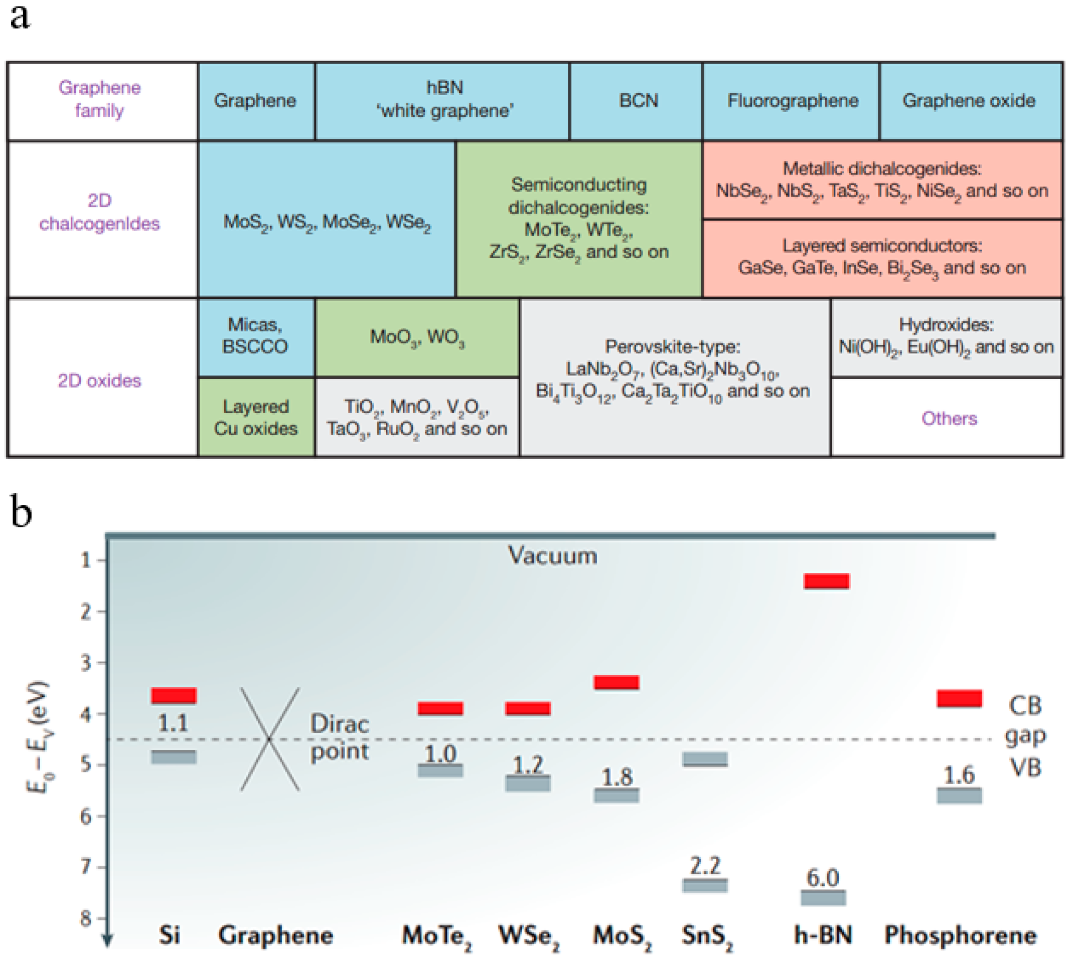
Two-dimensional materials, which constitute van der Waals heterostructures (vdWHs), have been explored to exhibit entirely different characteristics (Figure 2a), including conductors, semimetals, semiconductors, and insulators. Large group of two-dimensional materials provide various band gap and different electronic and optical performance, which offers the theoretical possibility of different device application requirement. With different 2D materials to form heterostructure, not only novel properties can be observed but also highly reliable nano-device can be achieved as well.
2.1. Graphene
With a honeycomb lattice structure assembled by strong covalent bond force, crystal structure shown in Figure 1d, graphene only has a single atomic carbon layer, which can be manufactured via mechanically exfoliating from bulk graphite. Due to bulk graphite has weak interlayer connection formed by van der Waals force, the large-area monolayer graphene can be easily and successfully exfoliated from bulk material with the help of a scotch tape. Owing to the unique lattice structure and atom combination, graphene has zero band gap which means charge carriers move in a ultrahigh speed about 25,000 cm2·V−1·s−1 at room temperature [24]. In other words, with high conductivity in 2DLMs family, graphene behaves like metal, which is the significant component of forming vdWHs. Transistors with graphene electrodes will have a lower contact resistance compared to transistors without graphene electrodes [25]. In flash memory devices, graphene also acts as charge trap layers [26]. Due to the single-atom thickness and specific density of state (DOS), it exhibits partial optical and electrostatic transparency under tunable work function. For possessing this characteristic, graphene serves as contact material integrated with other two-dimensional semiconductors in vdHW transistors, which achieves an appropriate contact resistance and admirable electrical performance [27].
Bilayer graphene, which is constituted of two atomic carbon-layers stacked by van der Waals interaction under specific direction, does not exhibit the same properties as monolayer graphene. That is because the interaction between two neighboring layers provides extra van der Waals electric field, which inducts bilayer’s bandgap [28] and forms four pseudospin flavors [29]. Although bilayer graphene has a band gap up to 250 mV under gate controlling, it is still smaller than other 2DLM like transition metal dichalcogenide, and even bulk Si (the band gap is about 1.2 eV). Even though monolayer graphene has zero band gap, it can be used in other ways such as graphene electrode in transistor, charge trap layer in flash memory and metal–graphene interfaces which can provide photo-generated carriers in photodetectors [30,31]. Moreover, bilayer graphene transistors also have a degradation of the carrier mobility compared with monolayer graphene [2].
2.2. Transition Metal Dichalcogenide
Transition metal dichalcogenide (TMDC) is the group of two-dimensional materials with chemical form MX2, where M stands for transition metal (molybdenum and tungsten) and X represents for the chalcogenide (sulfur, selenium or tellurium). The arrangement of atomic layered TMDC is X-M-X form. The crystal structure is shown in Figure 1f. Considering the same reason that adjacent layers of TMDC are weakly held together by van der Waals force, monolayers of TMDC can also be directly split from bulk crystals (regardless of artificiality or natural mineral) by scotch tape, called mechanical exfoliation, and it can also be fabricated by chemical vapor deposition (CVD) processes [32,33]. From bulk structure to two-dimensional layered structure, the most frequently studied TMDCs, such as MoS2, MoSe2, WS2 and WSe2, show various band gaps (Figure 2b) and tunable electronic properties with its volume changing from bulk material to monolayer [16]. At room temperature, as the thickness of TMDC decreases from bulk to monolayer, its band gap ranges from 1 eV to 2 eV and carrier mobility reaches over 100 cm2·V−1·s−1. Owing to the varied bandgap resulting in tunable electrical characteristics, there are some distinctive properties observed in TMDC, for example, valley Hall effect [34], valley polarization [35], superconductivity [36] and photoelectric characteristic [37,38]. TMDC’s lack of dangling bands is another reason that makes it attractive for use in FET channel material. This means the lattice mismatching is out of consideration during the formation of TMDC–TMDC van der Waals interconnection.
2.3. Phosphorene
Phosphorene is a monolayer material constituted of phosphorus, with a vertically interlaced hexagonal lattice that looks like armchairs. Phosphorene’s bandgap varies from 0.33 eV to 1.5 eV depending on the number of layers stacked [39]. Notably, an individual property is observed in few layers of phosphorene, i.e., anisotropic transportation in different phosphorene’s crystal orientations [40]. Specifically, transporting in the armchair direction (x direction) is much more efficient than in zigzag direction (Figure 1c). In addition, a p-type semiconductor characteristic emerges in phosphorene. When the hole mobility exceeds 1000 cm2·V−1·s−1 in certain direction [41], the phosphorene becomes the significant 2D material for electronic device. Later report shows that the drain current of FETs based on phosphorene can be modulated to 105, which means the Ion/Ioff ratio reaches 105 [42]. The tunable bandgap of phosphorene make it possible to react with different spectral regime from visible to infrared, which can be applied in fabricating multispectral photodetector [43].
The main challenge for phosphorene’s extensive application is the environmental stability, which means it can be easily oxidized [44]. To prevent the surface oxidization which leads to the decrease of device performance, some solutions have been adopted, for example, using h-BN [45], atomic layer of Al2O3 [46,47] and hydrophobic fluoropolymer [48] as encapsulating materials during process of van der Waals stacking.
2.4. Hexagonal Boron Nitride
Hexagonal boron nitride (h-BN), also called white graphite, has the same lattice structure as graphite. (Figure 1e) For boron and nitrogen are combined together by the strong covalent sp2 hybridized chemical bond, h-BN exists as insulator with a large bandgap of 6 eV [49]. Mechanical exfoliation can provide an atomically smooth surface without dangling bond and carrier traps, so a few layers of h-BN can be used as ultra-flat insulating substrates, the gate dielectrics [50] and ideal encapsulate material [24] in heterostructure transistors [13]. Besides, ultrathin h-BN can be served as great tunneling barrier material in tunneling devices [51,52].
2.5. Other Various 2D Materials for vdWHs
In the past few years, novel 2D TMDCs draw a lot of concentration on creating new types of devices; meanwhile, traditional 2D materials such as MoS2 and WSe2 have been considered once more. In virtue of doping technology, high-k amorphous titanium suboxide (ATO) is used as an n-type charge transfer dopant on the monolayer MoS2, which decreases the contact resistance to 180 Ω·µm [53]. Utilizing AlOx, another method of n-type doping in MoS2 is demonstrated, which can also reduce the contact resistance to 480 Ω·µm [54]. After confirming operational parameters of chemical vapor deposition, ultrathin MoS2(1−x)Se2x alloy nano-flakes with atomic or few-layer thickness can be obtained and it have high activity and durability during the hydrogen evolution reaction [55]. These various 2D materials show variable bandgaps, tunable optical and electronic properties [56,57].
3. Techniques
Two-dimensional materials can be assembled or grown directly into heterostructures, where the monolayers are held together by van der Waals forces. Although variety of 2D materials have been found, the assembly techniques currently used allow only certain types to build up the heterojunction. At the same time, the alternative technique, called sequential growth of monolayers, potentially do well in large scale production. Actually, the growth method has some limitations, such as slow growth and hard to control, and is still in early stages. Nevertheless, a great number of experiments with van der Waals heterostructure indicate that 2D materials are versatile and practical for further applications [58].
3.1. Assembly
Direct mechanical assembly is the most commonly used techniques of assembling heterostructures at present. This techniques was been put forward in 2010 by Dean et al., who demonstrated a very high level of performance provided by graphene and h-BN [13].
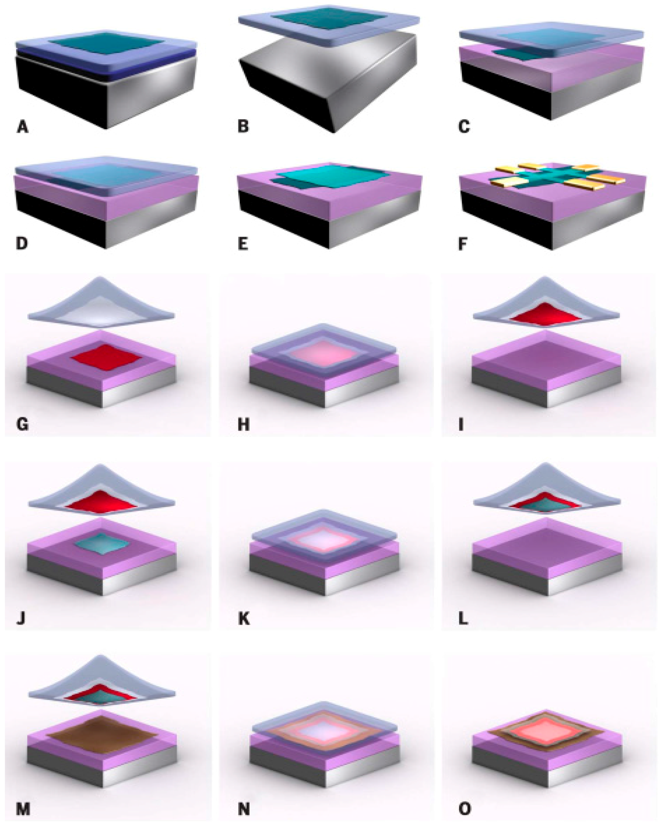
In early works, the technique is only used in preparing a flake of 2D material on a sacrificial membrane, such as PDMS, aligning and placing it on the substrate, and then remove or dissolve the membrane (Figure 3A–G). Then, the progress is repeated to deposit the other 2D material on the top of the former layer. Because the materials have close contact with the sacrificial layer, which is dissolved finally, the interface between TMDC and sacrificial layer will be contaminated. However, annealing can remove this contamination and achieve high interface quality, so the mobility of graphene device can reach 106 cm2·V−1·s−11 [13].
The other substantially cleaner method has the same principle that van der Waals interaction exist between layers. After sticking the first layer onto membrane, the second layer is directly stuck on the first layer, instead of dissolving the membrane (Figure 3G–O). Then, the process is repeated several times to get expected multilayer. This method leads to cleaner interface over large areas, and higher electron mobility.
3.2. Growth Methods
Although the assembly methods can stack the layers and achieve a clean interface, it still has some disadvantages, for example, the stacking position cannot be accurately controlled, which affects the device properties [22]. The direct growth of vertical layered heterostructures via chemical vapor deposition (CVD) is much more promising in terms of being controllable and scalable.
The direct growth of heterostructures can be divided into two parts: (1) sequential CVD growth of 2D materials layered; and (2) molecular beam epitaxy (MBE). The detailed information is presented in the following.
3.2.1. CVD
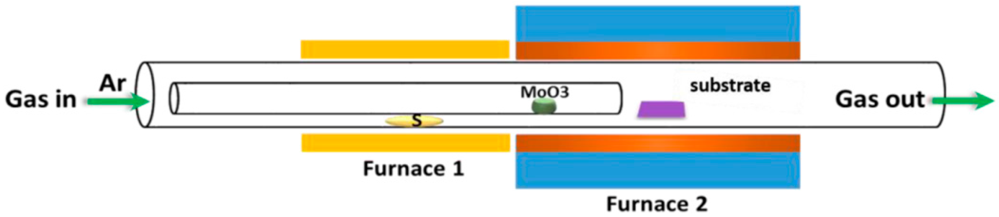
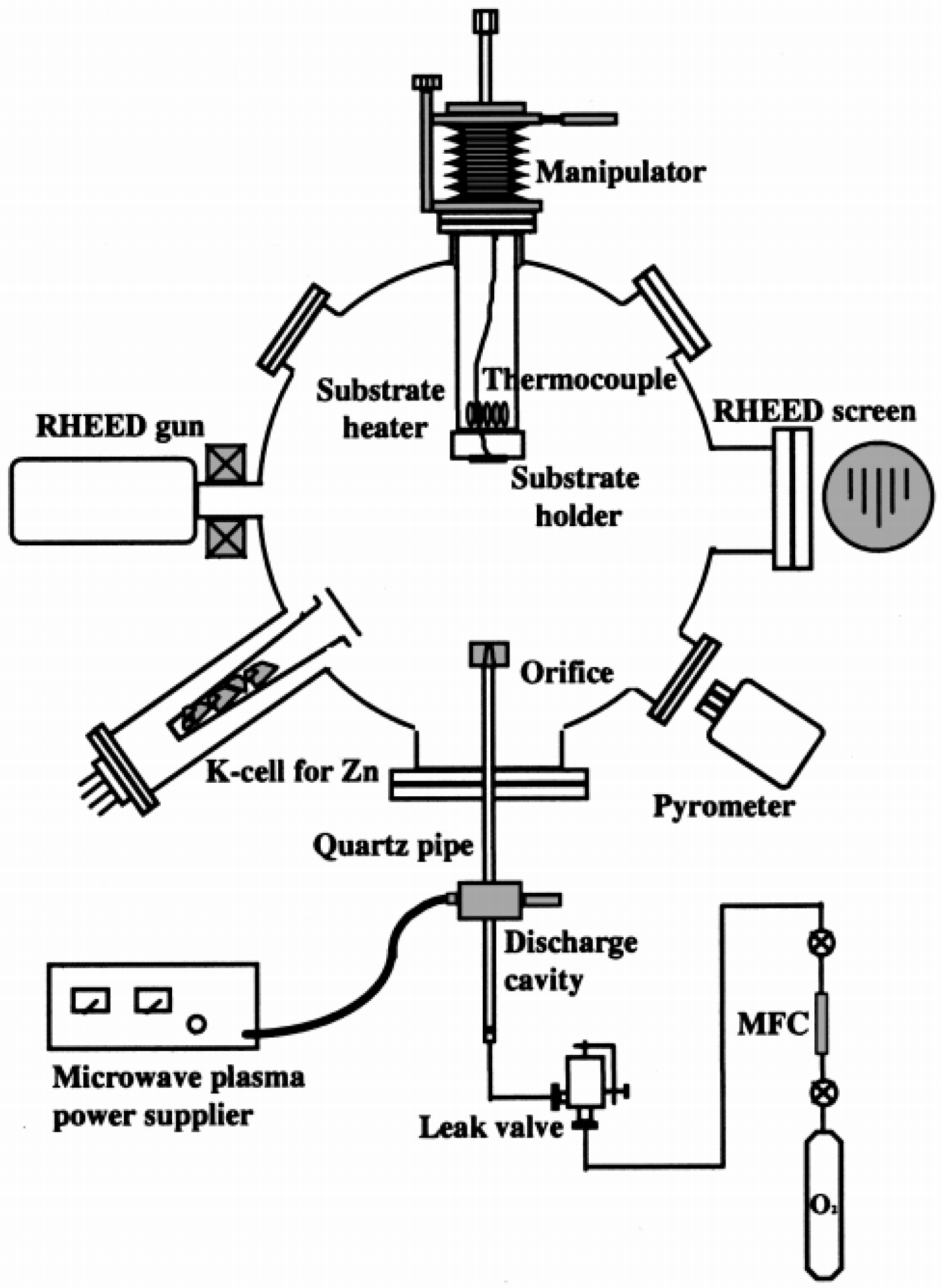
For the CVD system of MoS2 growth, as depicted in Figure 4, two separated furnaces are used to precisely control temperature applied on both precursors and substrate. Sulfur powder and the substrate are in the same pipe while different furnaces, where the interaction temperature can be independently controlled. Twenty milligrams of MoO3 powder, which temperature is dominated by furnace 2, is loaded between sulfur powder and the substrate and has an independent mini-pipe (diameter 1 cm). This is to prevent any cross-contamination and reaction between sulfur and MoO3, resulting in the decrease amount of MoO3 and unstable precursor supply in the vapor phase. Typical growth temperatures used for sulfur, MoO3, and the substrate are ~180 °C, ~300 °C, and ~800 °C, respectively. To ensure the sufficient supply of sulfur vapor in the system, it is preheated before increasing the temperature of MoO3.
This simple but scalable CVD growth approach can realize the direct fabrication of large-area MoS2/h-BN heterostructures with cleaner interface and better contact, compared with mechanical transfer method or assembly methods [59].
3.2.2. MBE
As one of the most commonly used growth methods of heterostructures, CVD has successfully accomplished several two-dimensional layered materials [60]. Although it is almost theoretically perfect, the reaction condition of CVD is hard to control at present and the results reported publicly can only form a few well-defined islands over the entire wafer. Considering the defects, MBE is an alternative approach for CVD in some ways [61].
As the name suggests, MBE is a kind of physical deposition method that takes place in ultrahigh vacuum. Figure 5 shows a typical MBE system. The required components are heated into vapor and sprayed on the substrate through a small hole. At the same time, a controlling molecule beam is used to scan the substrate line by line, and the molecules or atoms are arranged layer by layer in lattice structure. The ultra-high vacuum(UHV) environment minimize the contamination of the interface between substrate and growing flake. Because there are few particles in UHV environment, the ionized atoms and molecules traveled in nearly collision-free path until hitting the substrate or the chilled oven walls, where atoms condense immediately, and thus are effectively cleaned up from the reacting system without extra contamination. Because the components are sprayed onto substrate through a small hole, it can be turned off almost instantly and changed into another reactant whenever necessary. Most importantly, MBE growth can be simplistically described as “spray painting” the substrate crystal with layers of atoms, changing the composition or impurity in each layer until a desired structure is obtained [62].
Compared with CVD, MBE can potentially grow products overspread the whole wafer, precisely control the rate of interaction by means of regulating the rate of spraying and easily change the reactant as requirement. In this sense, MBE is almost the ideal method of vdWHs fabrication since the composition can be precisely controlled layer by layer.
4. FETs Based on Heterostructures Applications
Various 2D materials provide diverse electronic properties from conductors to insulators which benefits new devices creation. Van der Waals heterostructures exhibit ultrathin thickness and special properties that give a chance to build transistors at nanoscale size compared to bulk materials. Thus, novel field effect transistors based on van der Waals heterostructures have developed.
4.1. Decrease the Contact Resistance
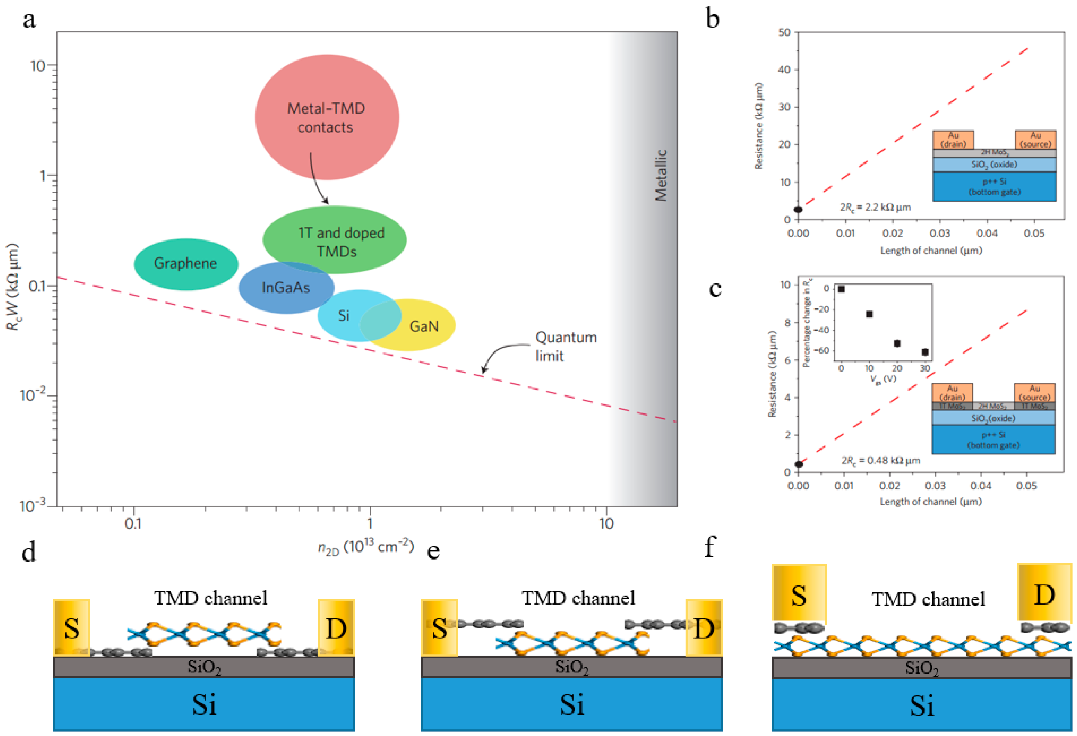
Two-dimensional semiconductors (2DSCs), especially TMDCs, have sparked immense interest in the electronic devices since the MoS2-based transistor was first reported [64]. Source and drain are often made of Metal-TMD directly contact, which induce a high contact resistance Rc. Even the contact resistance is larger than Si based transistors. The excessive contact resistance Rc on the source and drain interface is a great challenge for 2DSCs devices.
The high contact resistance, induced by a high Schottky barrier [65], prevent the charge carriers moving through the metal-semiconductor contacts. While the typical 2DLMs contact resistance currently achieved is 100 times higher than Si-based electronics (<20 Ω·μm) [66], there is still much work to do to decrease the actual contact resistance (Figure 6a). Some strategies have been used to reduce the contact resistance with the help of graphene/metal heterostructures. Schematics are shown in Figure 6d–f.
In silicon-based transistor, doping is conventionally used in traditional process of decreasing contact resistance at the source and drain interface, which is not reliable in TMDC-based transistor. That is because a highly doped silicon-based transistor can provide more carriers to fill valence band [65]. However, injecting other elements into TMDC seriously damages the covalent bonds between the atoms and breaks TMDC’s unique lattice structure, thus a great deal of defects are generated into layers resulting in Fermi-level pinning, which causes undesired contact resistance [68,69]. Besides TMDC, graphene is another 2DLM drawing extensive concern. The greatest contribution of graphene is forming van der Waals stacks with metal and 2DLM, which commendably decreases the contact resistance due to its special band structure. Because graphene is single-element 2DLM, it can be doped similar to silicon. Compared with intrinsic graphene, the highly-doped graphene decreases the height of Schottky barrier formed by the connection of graphene and metal, which means the contact resistance is greatly reduced [70]. A typical TMDC-based transistor, which uses monolayer graphene as metal electrodes, 2DLMs such as tungsten diselenide (WSe2) as semiconductor channel, and hexagonal boron nitride (h-BN) as gate dielectric, exhibits very high performance, such as high current on/off ratio, remarkable temperature stability, low contact resistance and low subthreshold slop [71]. Even though the Schottky barriers is still high (0.22 eV) at the graphene–WSe2 contact, the on-state current is dominated by tunneling through the barriers which makes the barriers almost transparent to the charge carriers. After using 3 nm h-BN as gate dielectric and 1.5 nm WSe2 flake as channel material, the tunneling distance is only 1.6 nm [72]. There are three types of interface of graphene–2DSCs contact: coplanar contacts (Figure 6d), staggered contacts (Figure 6e) and hybrid contacts (Figure 6f).
The coplanar structure is that the TMD channel materials and source/drain electrodes are on the same side of graphene. With the bottom graphene contact for 2DSCs transistors, nearly perfect work function matching lead to a barrier-free contact, which can significantly decrease Rc. MoS2 and WSe2 transistors using this strategy have been demonstrated [25,70,73,74]. Staggered contacts mean that TMD channel and source/drain electrodes are on different sides of graphene. With this strategy, transistors can be less susceptible to lithographic contamination, because the polymer residue did not touch TMD channel directly. Otherwise the residue will affect the charge transport at the interface. With this method, high performance MoS2 transistors [75,76,77,78] and air stable black phosphorus transistors [45] have been reported. Metal–graphene hybrid structure as a unique contact to reach minimized Rc (300 Ω·μm) compared to metal–TMD structure. With graphene inserted as the interlayer buffer, the carrier injection was enhanced at metal–graphene–TMD channel interfaces. For example, nickel–etched–graphene electrodes have achieved a relatively low resistance [79]; Ti–graphene–MoS2 stacks can ruduce Rc from 12.1 ± 1.2 Ω·mm to 3.7 ± 0.3 Ω·mm to some degree compared with stacking Ti onto MoS2 directly [80].
When integrating two-dimensional transition metal dichalcogenides with metal, the valence band shows unusual Fermi level pinning. Compared with chemical doping, which will destroy the covalent bond of TMDs within layers, the stacking of graphene can create a undamaged van der Waals contact and a ultraclean interface, which prevents Fermi level pinning [25,75]. There are some other reports demonstrate a stacking structure formed by MoS2 and graphene to reduce the connect resistance [73,77,81]. In this structure, graphene and metal are connected together to form electrodes and molybdenum disulfide (MoS2) is used as channel. The tunability of doping graphene’s work function can significantly improve the ohmic contact to MoS2 [77].
Besides graphene, other 2DLMs such as MoS2 can also be doped with element to improve the mobility of charge carriers which leads to low contact resistance, for example, physisorbing chloride molecule into WS2 or MoS2 [82]. With the method of physisorbed molecules, contact resistance can be obviously decreased [83]. Other efforts of contacting electrode metal materials with TMDs create the low Schottky barrier. For example, the connection between molybdenum (Mo) and MoS2 forms perfect interface, leading to ultralow Schottky barrier about 0.1 eV [84]. Other methods based on van der Waals heterostructure to decrease Rc have include phase-engineering. With the organolithium chemical method, MoS2 changes from 1T phase to 2H phase. 2H phase MoS2 behaves as electronic channel, as shown in Figure 6b. This 1T–2H–1T structure can receive relatively low Rc [67] (Figure 6c). To create stable homojunction contact of MoTe2, some reports use laser to achieve two phase interconversion. Stacking semiconducting hexagonal (2H) and metallic monoclinic (1T) MoTe2 together can fabricate an ohmic heterophase homojunction, which is necessary in lowing contact resistance [67]. Phase engineering, therefore, provide a way of creating lateral heterostructures with low resistance, but additional work is needed to achieve values comparable to state-of-art materials and close to the quantum limit.
4.2. Tunneling Field Effect Transistor and Barrister
The principle of tunneling field effect transistors (TFETs) is band-to-band tunneling [85]. The barriers induce by van der Waals gap narrow because the width of van der Waals gap is below 1 nm, which will lead to charge carriers tunneling [86]. For width of barriers narrowing at the contact interface, the tunneling current between source and drain increases rapidly in silicon-based transistor. However, vertical tunneling transistor based on vdWHs is different from conventional TEFTs. In vertical structure, two separate monolayers of graphene serve as electrodes, and ultrathin dielectric material are stuck between them. Based on gate-voltage tunability of the DOS in graphene, the height of Schottky barrier reduces and realizes the charge carriers’ transportation.
Transistors based on that principle use very thin BN (1.4 nm) and MoS2 as vertical transport barrier, making devices have the switching ratio of ~10,000 at room temperature [87]. Further study of this type of heterostructure is the resonant tunneling and gate voltage-tunable negative differential conductance [88]. Other studies have put forward how to achieve the resonant tunneling with the help of crystallographic orientation alignment of the graphene-BN-graphene heterostructure [89,90].
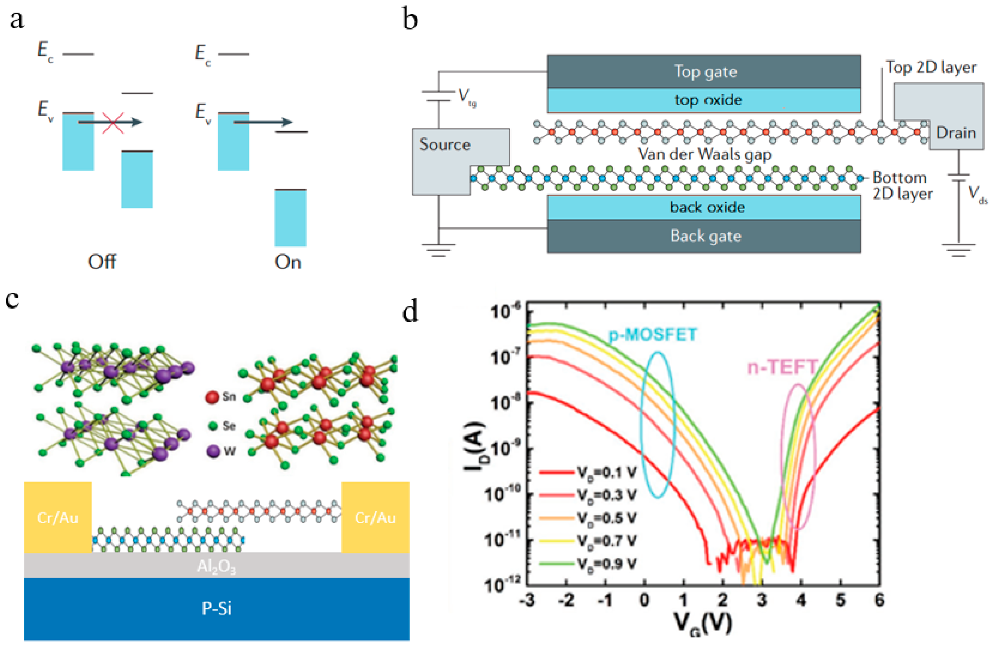
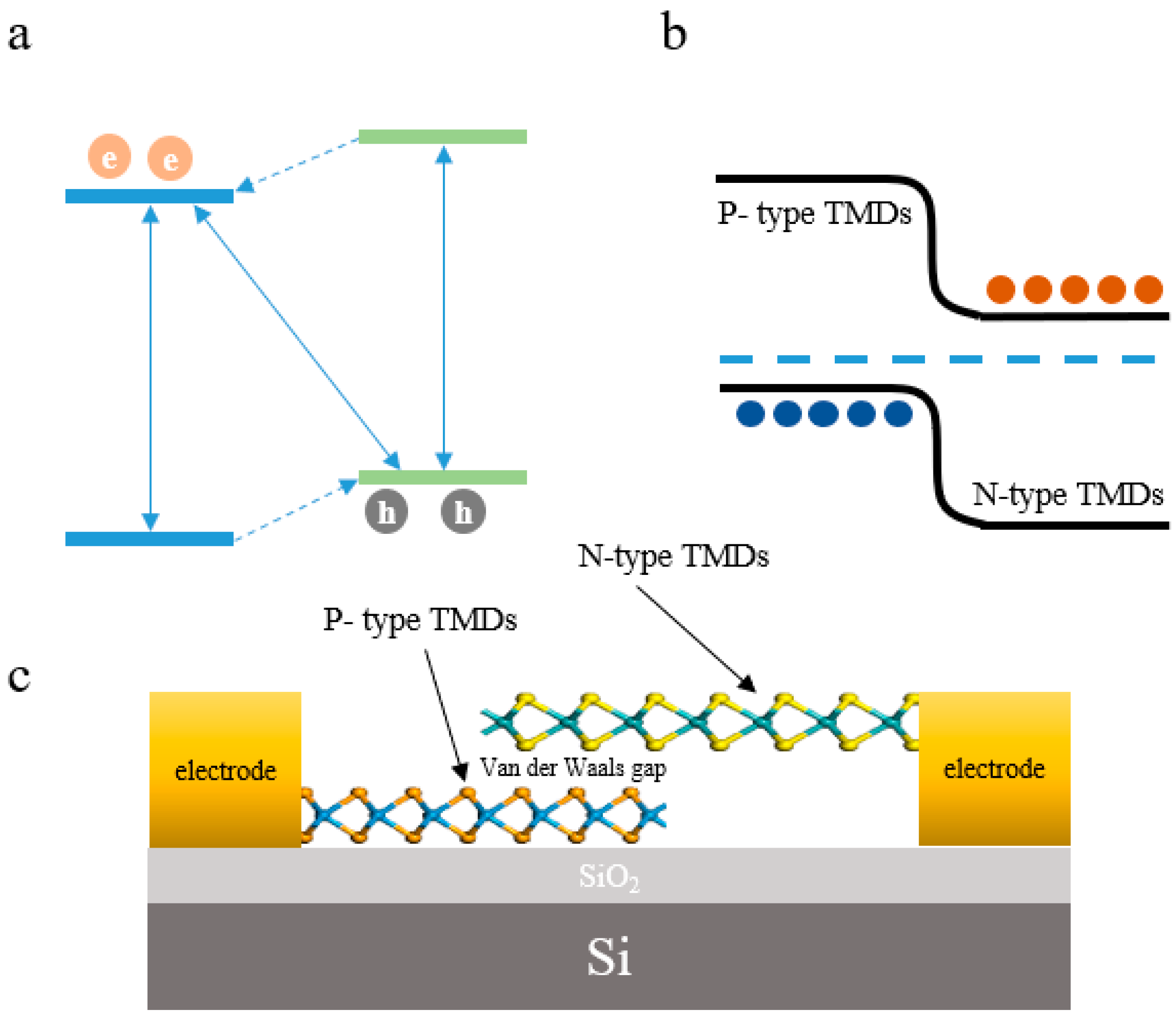
In addition of graphene, two dimensional TMDs have sharp band edges and ultra-narrow channel length, which has been the suitable candidates for TFETs. By correctly choosing two 2D layers of semiconductors to make up a suitable heterojunction (one layer is n-type and the other layer is p-type), it can achieve both large tunneling current and low subthreshold swing (SS). Subthreshold swing (SS) shows the current transformation with the change of voltage, when the device works in subthreshold state. With the proper heterojunction band offsets between the two 2D semiconductor layers (Figure 7a,b), the tunneling current will be significantly increased because of the band alignments. TFETs with SnSe2/WSe2 van der Waals heterostructure (Figure 7c) have achieved the SS of 80 mV/dec at room temperature and ION/IOFF ratio exceeding 106 [91] (Figure 7d). In addition, dual-gated MoS2/WSe2 van der Waals heterostructures were demonstrated and carrier concentration of MoS2 and WSe2 can be independently controlled by up and down symmetric gates, which achieved a high efficiency of 80% due to the weak electrostatic barrier through atomic layers [92].
4.3. Van der Waals Heterostructure Based Vertical Transistors (VFETs)
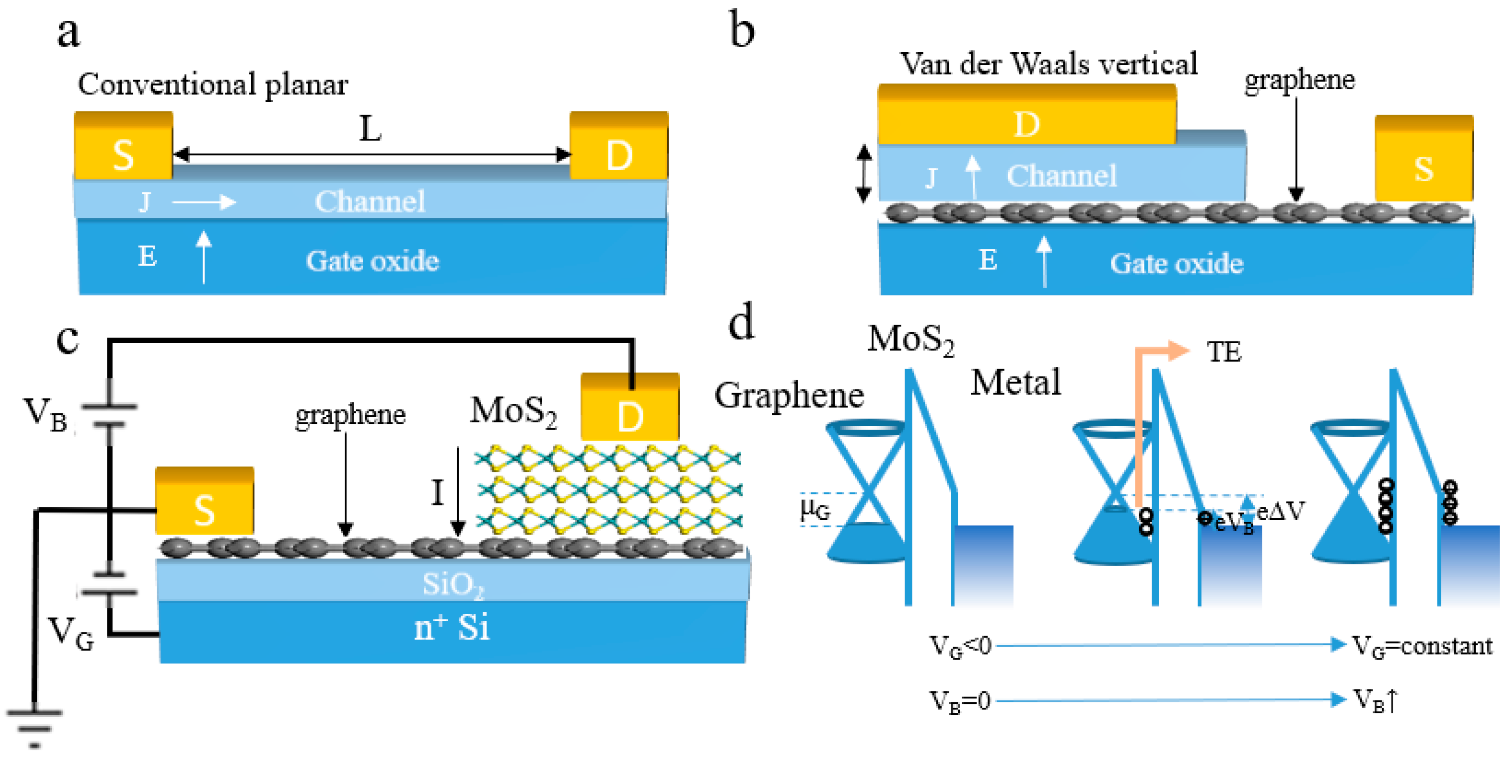
With ultrathin structure and suitable band structure, 2DLMs can create totally new devices such as vertical transistors. Compared with conventional planar field effect transistors, which consist of a source and a drain plate electrode with a conducting channel located between them, vertical transistors often use graphene and metal as source and drain electrodes, respectively. In planar transistors (Figure 8a), the gate electrical field (E) controls the channel carriers to influx. Thus, the channel current density (J) is always perpendicular to the gate electrical field (E) (J⊥E). The channel length is decided by the area of 2DSCs. In other word, the lithographic accuracy which decides the distance of source and drain would influence the channel length. In particular, the tunable work function and partial electrostatic transparency make graphene become the appropriate candidate of interconnecting with semiconductor to fabricate vertical transistors, in which graphene acts as the active contact. In this fundamentally different geometry, as shown in Figure 8b, the channel carriers transport direction is parallel to the gate electrical field (J∥E). The channel length is decided by the thickness of 2DSCs which can be prominently shorter than the planar transistors. With effectively modulating the work function of graphene by introducing the gate voltage, the Schottky barrier between graphene and semiconductor changed and result in large current injection, which brings a large on/off ratio that cannot be achieved in planar transistors.
Different kinds of transistors based on vertical vdWHs have been reported according to its special device structure. N-channel vertical FET created by sandwiching multilayered MoS2 between graphene and metal panel (Figure 8c), has the on/off ratio >103 at room temperature [93]. Due to van der Waals interface between MoS2 and graphene, the Schottky barrier restrains current injection. Introducing an external electric field can strongly modulate the height of Schottky barrier owing to the small density of states of graphene [94]. The band structure of graphene/MoS2/metal heterostructure is shown in Figure 8d. The source/drain voltage (VB) drives current follow vertically into multilayered MoS2 channel. The carriers transport is dominated by thermionic-emission (TE). The application of VB changes the Fermi level in graphene due to the capacitive coupling through MoS2. With the increasing VB, the Fermi level will reach the Dirac point at some point, as shown in the right panel of Figure 8d [95,96]. Other 2DLMs such as WS2 possessing the same geometrical structure of MoS2 VFETs have been reported, achieving extremely large on-state current [97].
As graphene has attracted increasing attention among researchers, other carbon-based materials such as fullerene also draw attention to be assembled with graphene or 2DLMs to create organic vertical field effect transistors (OVFETs). In other words, the work function of fullerene (C60) is closed to graphene. Thus, the graphene/C60/metal VFET with a measured current on/off ratio up to 105 has been reported [98] and the logic inverter based on this structure also has been reported yet [99]. Some types of organic or molecular crystals can act as semiconductor. After stacking on graphene to form 2D–3D heterojunction, which is an excellent vertical channel for VFETs, new opportunities in developing novel OVFETs exist. At the same time, organic transistors such as 2D quasi-freestanding molecular based graphene transistors which had the mobility up to 10 cm2·V−1·s−1 have been achieved [100].
4.4. Photodetector and Diodes Based on van der Waals Heterostructure
Based on fine optical characteristic of two-dimensional TMDCs, photovoltaic applications about van der Waals heterostructure combined with such materials have been explored. The typical application is the photodetectors made of graphene act as channel material and MoS2 act as light sensitive material [101]. Under the combination of two kinds of 2D materials which have different tunable work functions, photoexcited electrons and holes can be accumulated in conductor layers. Shown in Figure 9a, photoexcited pairs have been observed in the heterostructure of MoS2/WSe2 [102] and MoSe2/WSe2 [103]. Most photovoltaic devices can be created by combining few layers of TMDCs with graphene. Using graphene as electrodes and TMDCs sandwiched between two graphene electrodes, one can create efficient photoexcited carriers inject into graphene electrodes [104,105]. In other words, graphene can form a typical ohmic contacts which will significantly decrease the resistance and serve as a transparent electrode.
If p-type and n-type 2D semiconductors stack together with van der Waals force, then atomic layers of p-n junctions can be acquired. Gate tunable diode based on TMDCs have been abundantly created. Various combinations of 2D semiconductors were used to construct p-n junction for photodetectors (typical p-n structure and band structure shown in Figure 9b) to realize the excellent performance of responsivity and detectivity [106,107,108,109,110,111,112]. Heterostructures such as MoS2/WSe2 [107], black phosphorus/MoS2 [109], and MoS2/WS2 [110] p-n junctions are widely used in photodetectors. GaTe/MoS2 heterostructure received a high photovoltaic performance whose photoresponsivity can reach 21.83 AW−1 [112].
4.5. Memory
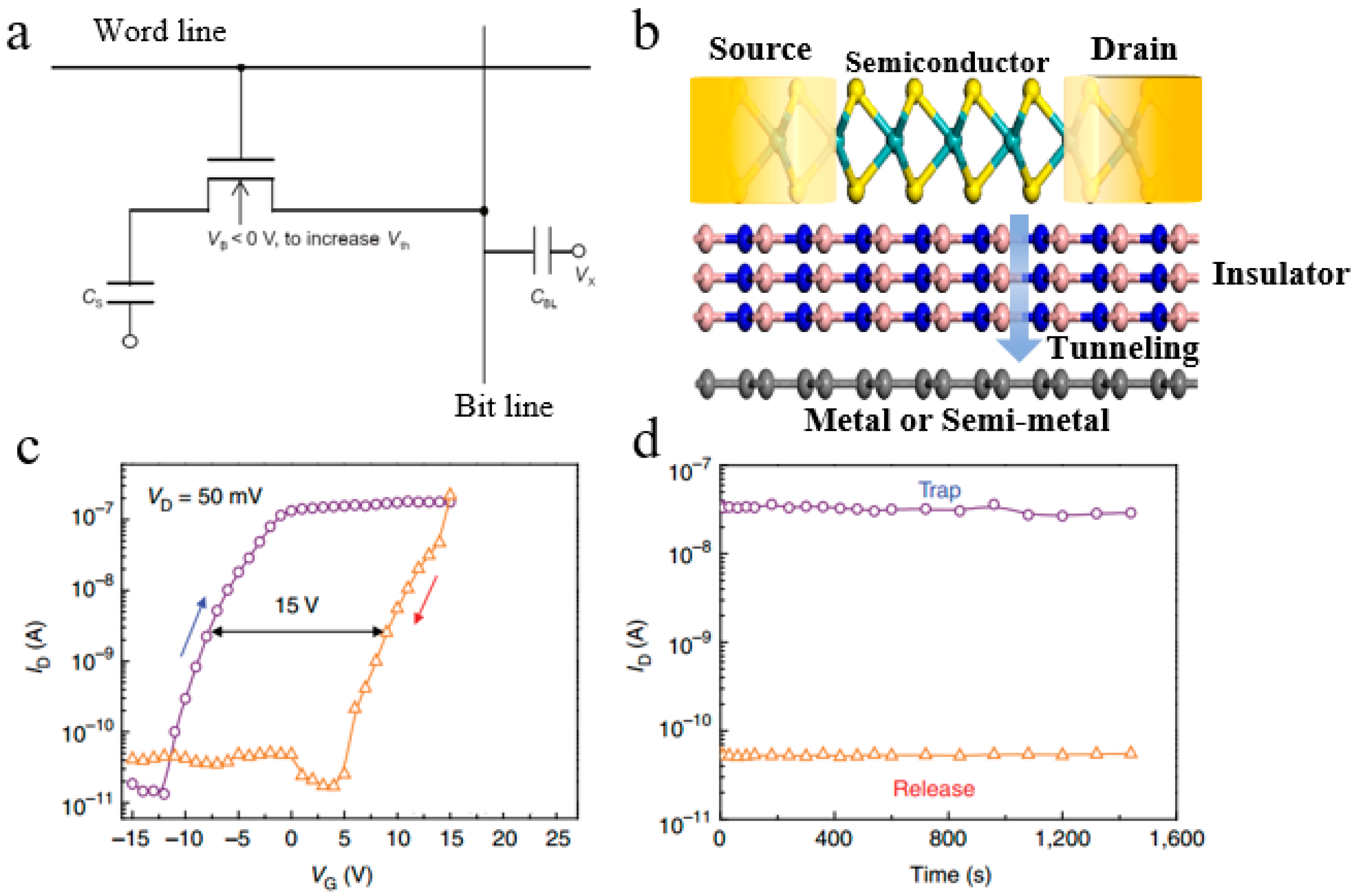
There are many types of memory devices which include dynamic random access memory (DRAM), static random access memory (SRAM), resistive random access memory (RRAM) and flash memory. The memory cells of DRAM and SRAM are based on the one-transistor and one-capacitance (1T1C) structure and six transistors (6T), respectively. The 1T1C DRAM cell is shown in Figure 10a. The capacitance charging and discharging controlled by the transistor on-state and off-state. When the word line voltage reaches the transistor on-state voltage, the current will follow through transistor and charge the capacitance when the bit line voltage is at high potential. This operation is called the programming process. When the bit line voltage is at low potential, the charged capacitance will discharge and the current will follow through the transistor into bit line, which is called erasing process. When the word line voltage controls transistor at the off-state, the charge carriers will be held in capacitance. After setting bit line at half of the high potential, the voltage will rise if the capacitance is charged and will decline if the capacitance is discharged. This is called the reading operation of DRAM. However, DRAM is a typical volatile memory, which means that the storage performance will disappear under the power-down state.
A new concept of constructing memory is based on the domain wall motion which means that crystalline particles with the same polarization direction as the external electric or magnetic field inside the crystal become larger. This process is done by the movement of domain wall. Current driven domain wall motion and electrically controlling the magnetization switching by spin orbit torque have been proposed for information storage. Decreasing the current density to realize the domain wall motion plays an important role in practical applications [114]. Basically, the external magnetic field is necessary to control the current-induced magnetization switching direction by spin orbit torque [115,116]. Later research has reported that the electric field definitively control the current induced ferromagnet switching at room temperature with the polarized ferroelectric substrate [117]. Piezo voltage solely controlling the magnetization switching at room temperature without external magnetic field has been realized, which can largely decrease the energy consumption compared with the electric current switching magnetization [118]. This concept offers an idea to develop ferroelectric random access memory, magnetic random access memory and phase change random access memory.
Another block of memory is flash, a kind of non-volatile memory. Flash memory is based on 2D material stacks established on a semiconductor–insulator–metal (SIM) structure (Figure 10b). MoS2/BN/Graphene heterostructure for use in flash memory has been widely explored [113,119]. Graphene and MoS2 were utilized as charge trapping layers and channel layers and h-BN acted as a tunnel barrier, respectively. Under a considerable voltage positive bias, the tunneling current exponentially increases with the decreasing of BN thickness, which will lead to the increasing charge injection into the trap layer. Thus, the thickness of insulator becomes especially important in SIM structure. The critical thickness of tunneling barrier is 7 nm. Tunneling current cannot be formed in the thick layers (>10 nm), while leakage current will exist in the thinner layers (3.5 nm), which will cause charging process failure [113]. When gate voltage becomes negative in releasing process, charge carriers trapped in the graphene layer will be transferred into MoS2. Thus, the charge retention and gate hysteresis that contains a memory window can be observed (Figure 10c). Retention time of trapping and releasing current shows the endurance of charge trapping flash device (Figure 10d). Detailed band is structure shown in Figure 11a with the charging and releasing process.
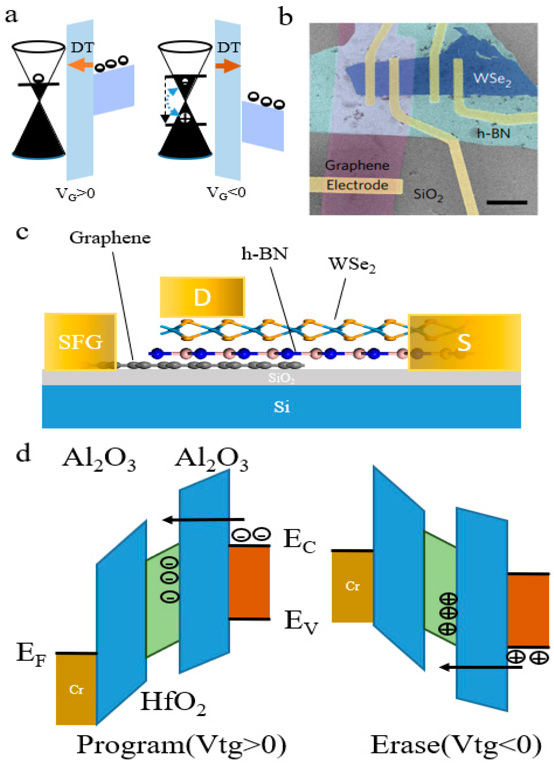
Nonvolatile floating gate flash memory based on black phosphorus/BN/MoS2 stacks have been reported, where MoS2 behaves as charge trapping layer and black phosphorus acts as channel [120]. Charge trap memory with high k dielectric materials can greatly improve the storage performance. Few-layer MoS2 channel and three-dimensional Al2O3/HfO2/Al2O3 stack together to form a charge trap flash memory device, exhibiting an unprecedented gate window of 20 V and a program/erase current ratio of 104 [121]. Band diagram of program/erase state of device under different top gate bias (Vtg) is shown in Figure 11d. Positive Vtg carry out the programming process. Electrons tunneling from MoS2 channel are accumulated in HfO2 charge-trap layer. Negative Vtg carry out the erasing process. Holes tunnel from MoS2 channel to HfO2 charge-trap layer. The charge-trap layer holds different charges, causing the threshold shifting. Thus, memory window exists. Besides MoS2 channel based charge-trap memory, Ambipolar WSe2 channel based charge-trap memory devices have also been reported [122]. Subsequently, black phosphorus based charge-trap memory devices with a Al2O3/HfO2/Al2O3 charge trap stack have been demonstrated, where the long data retention with only 30% charge loss after 10 years were obtained [123]. Beside floating gate memory, novel structure based on vertically stacked 2D materials (WSe2/h-BN/graphene) has the gate metal stack directly on the graphene, thus we call it semi-floating gate (SFG) flash memory [124]. The structure is shown in Figure 11b,c. When a positive voltage is applied on Si, electrons are accumulated in the WSe2. These electrons tunnel through BN and begin to be accumulated in graphene due to the different potential between WSe2 and graphene which is considered as programing process. When the positive bias is removed, electrons are still trapped in graphene due to the potential barriers of h-BN. When applying a small negative voltage bias on Si, the electrons tunnel through BN and are injected into WSe2 channel as an erasing process. Similar behaviors can be observed for holes when a negative voltage is applied on Si. When treated with plasmas, multilayer MoS2 transistors can serve as nonvolatile, highly durable flash memory with multibit data storage capability. This novel multibit flash memory is desirable for improving data storage density in order to reach manufacturing process [125].
Memory have made significant progress due to the multiduty van der Waals heterostructures. New type of memory devices structure began to spring up. However, effort still needs to be made to improve the memory performance such as stability, reliability and time of memory operation. 2D van der Waals heterostructures offer a new route of building novel memory.
5. Perspective
The inherent absolute advantages of 2D materials—exhibiting free of dangling bond and gate tunable electronic properties—make them promising candidates for van der Waals stacks, which are widely used in novel device design. However, the burgeoning van der Waals heterostructures applied to electronic devices remain in their infancy. Technical improvement still needs to be explored in the following effort.
Conventional laboratory-stage process of assembling van der Waals stack is mechanical exfoliation and transfer methods. The shape of exfoliated 2D materials is irregular and the size can only reach micron order. It is hard to acquire monolayer materials and most are few layers. Large area 2D materials are still needed in some cases during transfer process. Although with the utilize of chemical vapor deposition, large-scale synthesizing 2D materials and van der Waals heterostructures is developed, it still cannot be applied in integrated technique and lacks controllability of the relative orientation, size, shape and interlayer spacing with increasing vdWH layers. Furthermore, the electrical performance of chemically synthesized 2DLMs is inferior to their exfoliated counterpart. Thus, there is still much room to improve the process of assembling van der Waals heterostructure.
FETs based on van der Waals heterostructures have largely focused on attaining high performance with certain parameter to measure. However, parameters such as low SS at extensive range of gate voltage biases, which will lead to large on/off ratios with low input voltage biases, have become important criteria for measuring the performance of the devices. Besides, contact resistance is still a big deal for limiting the improvement of devices. There is still plenty of room to lower the contact resistance, as it is still above theoretical minimum, even larger than Si based transistors. The contact resistance must be lower by at least an order of magnitude to <100 Ω·μm. In 2D TMDCs, based on phase engineering, changing semiconductor to metal phases is a promising route of creating an ohmic contact which can greatly lower the contact resistance. In addition, the majority of TMDCs are unipolar, n-type or p-type. Controllable and stable doping process is still a major challenge to overcome the achievement of bipolar—both n-type and p-type—semiconductors or van der Waals stack of homogenous material, which will enable the next generation of high speed and low power devices. Direct growth of homogenous 2D semiconductor with stable doping process to form different types of heterostructures and phase engineering to decrease contact resistance are topics for future research. Scalable fabrication of van der Waals stacks also need to be explored. Creating new structure of semiconductor devices based on van der Waals heterostructures still has a long way to go.
Acknowledgments
This work was supported by the National Natural Science Foundation of China (61622401, 61734003, and 61376093) and National Key Research and Development Program (2017YFB0405600 and 2016YFA0203900).
Author Contributions
Jingyu Li conceived and designed the workflow of the paper. Jingyu Li performed the literature search, collected the data meeting the criteria, performed the schematic diagram analysis and figures. Jingyu Li and Xiaozhang Chen wrote the paper. All authors revised the manuscript.
Conflicts of Interest
The authors declare no conflict of interest.
References
- Novoselov, K.S.; Fal, V.; Colombo, L.; Gellert, P.; Schwab, M.; Kim, K. A roadmap for graphene. Nature 2012, 490, 192–200. [Google Scholar] [CrossRef] [PubMed]
- Schwierz, F. Graphene transistors. Nat. Nanotechnol. 2010, 5, 487–496. [Google Scholar] [CrossRef] [PubMed]
- Weiss, N.O.; Zhou, H.; Liao, L.; Liu, Y.; Jiang, S.; Huang, Y.; Duan, X. Graphene: An emerging electronic material. Adv. Mater. 2012, 24, 5782–5825. [Google Scholar] [CrossRef] [PubMed]
- Liao, L.; Bai, J.; Cheng, R.; Lin, Y.-C.; Jiang, S.; Qu, Y.; Huang, Y.; Duan, X. Sub-100 nm channel length graphene transistors. Nano Lett. 2010, 10, 3952–3956. [Google Scholar] [CrossRef] [PubMed]
- Liu, Y.; Weiss, N.O.; Duan, X.; Cheng, H.-C.; Huang, Y.; Duan, X. Van der Waals heterostructures and devices. Nat. Rev. Mater. 2016, 1, 16042. [Google Scholar] [CrossRef]
- Chhowalla, M.; Jena, D.; Zhang, H. Two-dimensional semiconductors for transistors. Nat. Rev. Mater. 2016, 1, 16052. [Google Scholar] [CrossRef]
- Novoselov, K.; Jiang, D.; Schedin, F.; Booth, T.; Khotkevich, V.; Morozov, S.; Geim, A. Two-dimensional atomic crystals. Proc. Natl. Acad. Sci. USA 2005, 102, 10451–10453. [Google Scholar] [CrossRef] [PubMed]
- Jariwala, D.; Marks, T.J.; Hersam, M.C. Mixed-dimensional van der Waals heterostructures. Nat. Mater. 2016, 16, 170. [Google Scholar] [CrossRef] [PubMed]
- Liu, Y.; Cheng, R.; Liao, L.; Zhou, H.; Bai, J.; Liu, G.; Liu, L.; Huang, Y.; Duan, X. Plasmon resonance enhanced multicolour photodetection by graphene. Nat. Commun. 2011, 2, 579. [Google Scholar] [CrossRef] [PubMed]
- Konstantatos, G.; Badioli, M.; Gaudreau, L.; Osmond, J.; Bernechea, M.; De Arquer, F.P.G.; Gatti, F.; Koppens, F.H. Hybrid graphene-quantum dot phototransistors with ultrahigh gain. Nat. Nanotechnol. 2012, 7, 363–368. [Google Scholar] [CrossRef] [PubMed]
- Liao, L.; Bai, J.; Qu, Y.; Lin, Y.-C.; Li, Y.; Huang, Y.; Duan, X. High-κ oxide nanoribbons as gate dielectrics for high mobility top-gated graphene transistors. Proc. Natl. Acad. Sci. USA 2010, 107, 6711–6715. [Google Scholar] [CrossRef] [PubMed]
- Liao, L.; Lin, Y.-C.; Bao, M.; Cheng, R.; Bai, J.; Liu, Y.; Qu, Y.; Wang, K.L.; Huang, Y.; Duan, X. High speed graphene transistors with a self-aligned nanowire gate. Nature 2010, 467, 305. [Google Scholar] [CrossRef] [PubMed]
- Dean, C.R.; Young, A.F.; Meric, I.; Lee, C.; Wang, L.; Sorgenfrei, S.; Watanabe, K.; Taniguchi, T.; Kim, P.; Shepard, K.L. Boron nitride substrates for high-quality graphene electronics. Nat. Nanotechnol. 2010, 5, 722–726. [Google Scholar] [CrossRef] [PubMed]
- Withers, F.; Del Pozo-Zamudio, O.; Mishchenko, A.; Rooney, A.; Gholinia, A.; Watanabe, K.; Taniguchi, T.; Haigh, S.; Geim, A.; Tartakovskii, A. Light-emitting diodes by band-structure engineering in van der Waals heterostructures. Nat. Mater. 2015, 14, 301–306. [Google Scholar] [CrossRef] [PubMed]
- Yang, H.; Heo, J.; Park, S.; Song, H.J.; Seo, D.H.; Byun, K.-E.; Kim, P.; Yoo, I.; Chung, H.-J.; Kim, K. Graphene barristor, a triode device with a gate-controlled schottky barrier. Science 2012, 336, 1140–1143. [Google Scholar] [CrossRef] [PubMed]
- Vaziri, S.; Smith, A.D.; Östling, M.; Lupina, G.; Dabrowski, J.; Lippert, G.; Mehr, W.; Driussi, F.; Venica, S.; Di Lecce, V. Going ballistic: Graphene hot electron transistors. Solid State Commun. 2015, 224, 64–75. [Google Scholar] [CrossRef]
- Jeong, H.; Bang, S.; Oh, H.M.; Jeong, H.J.; An, S.-J.; Han, G.H.; Kim, H.; Kim, K.K.; Park, J.C.; Lee, Y.H. Semiconductor–insulator–semiconductor diode consisting of monolayer MoS2, h-BN, and GaN heterostructure. ACS Nano 2015, 9, 10032–10038. [Google Scholar] [CrossRef] [PubMed]
- Sarkar, D.; Xie, X.; Liu, W.; Cao, W.; Kang, J.; Gong, Y.; Kraemer, S.; Ajayan, P.M.; Banerjee, K. A subthermionic tunnel field-effect transistor with an atomically thin channel. Nature 2015, 526, 91–95. [Google Scholar] [CrossRef] [PubMed]
- Zhang, Z.; Chen, P.; Duan, X.; Zang, K.; Luo, J.; Duan, X. Robust epitaxial growth of two-dimensional heterostructures, multiheterostructures, and superlattices. Science 2017, 357, 788–792. [Google Scholar] [CrossRef] [PubMed]
- Duan, X.; Wang, C.; Shaw, J.C.; Cheng, R.; Chen, Y.; Li, H.; Wu, X.; Tang, Y.; Zhang, Q.; Pan, A. Lateral epitaxial growth of two-dimensional layered semiconductor heterojunctions. Nat. Nanotechnol. 2014, 9, 1024–1030. [Google Scholar] [CrossRef] [PubMed]
- Gong, Y.; Lin, J.; Wang, X.; Shi, G.; Lei, S.; Lin, Z.; Zou, X.; Ye, G.; Vajtai, R.; Yakobson, B.I. Vertical and in-plane heterostructures from WS2/MoS2 monolayers. Nat. Mater. 2014, 13, 1135–1142. [Google Scholar] [CrossRef] [PubMed]
- Geim, A.K.; Grigorieva, I.V. Van der Waals heterostructures. Nature 2013, 499, 419–425. [Google Scholar] [CrossRef] [PubMed]
- Jena, D. Tunneling transistors based on graphene and 2-D crystals. Proc. IEEE 2013, 101, 1585–1602. [Google Scholar] [CrossRef]
- Mayorov, A.S.; Gorbachev, R.V.; Morozov, S.V.; Britnell, L.; Jalil, R.; Ponomarenko, L.A.; Blake, P.; Novoselov, K.S.; Watanabe, K.; Taniguchi, T. Micrometer-scale ballistic transport in encapsulated graphene at room temperature. Nano Lett. 2011, 11, 2396–2399. [Google Scholar] [CrossRef] [PubMed]
- Liu, Y.; Wu, H.; Cheng, H.-C.; Yang, S.; Zhu, E.; He, Q.; Ding, M.; Li, D.; Guo, J.; Weiss, N.O. Toward barrier free contact to molybdenum disulfide using graphene electrodes. Nano Lett. 2015, 15, 3030–3034. [Google Scholar] [CrossRef] [PubMed]
- Bertolazzi, S.; Krasnozhon, D.; Kis, A. Nonvolatile memory cells based on MoS2/graphene heterostructures. ACS Nano 2013, 7, 3246–3252. [Google Scholar] [CrossRef] [PubMed]
- Neto, A.C.; Guinea, F.; Peres, N.M.; Novoselov, K.S.; Geim, A.K. The electronic properties of graphene. Rev. Mod. Phys. 2009, 81, 109. [Google Scholar] [CrossRef]
- Zhang, Y.; Tang, T.-T.; Girit, C.; Hao, Z.; Martin, M.C.; Zettl, A.; Crommie, M.F.; Shen, Y.R.; Wang, F. Direct observation of a widely tunable bandgap in bilayer graphene. Nature 2009, 459, 820. [Google Scholar] [CrossRef] [PubMed]
- Novoselov, K.S.; McCann, E.; Morozov, S.V.; Falko, V.I.; Katsnelson, M.I.; Zeitler, U.; Jiang, D.; Schedin, F.; Geim, A.K. Unconventional quantum hall effect and berry’s phase of 2π in bilayer graphene. Nat. Phys. 2006, 2, 177. [Google Scholar] [CrossRef] [Green Version]
- Xia, F.; Mueller, T.; Lin, Y.-M.; Valdes-Garcia, A.; Avouris, P. Ultrafast graphene photodetector. Nat. Nanotechnol. 2009, 4, 839–843. [Google Scholar] [CrossRef] [PubMed]
- Mueller, T.; Xia, F.; Avouris, P. Graphene photodetectors for high-speed optical communications. Nat. Photonics 2010, 4, 297–301. [Google Scholar] [CrossRef]
- Wang, X.; Xia, F. Van der Waals heterostructures: Stacked 2D materials shed light. Nat. Mater. 2015, 14, 264. [Google Scholar] [CrossRef] [PubMed]
- Reale, F.; Sharda, K.; Mattevi, C. From bulk crystals to atomically thin layers of group vi-transition metal dichalcogenides vapour phase synthesis. Appl. Mater. Today 2016, 3, 11–22. [Google Scholar] [CrossRef]
- Mak, K.F.; McGill, K.L.; Park, J.; McEuen, P.L. The valley hall effect in MoS2 transistors. Science 2014, 344, 1489–1492. [Google Scholar] [CrossRef] [PubMed]
- Zeng, H.; Dai, J.; Yao, W.; Xiao, D.; Cui, X. Valley polarization in MoS2 monolayers by optical pumping. Nat. Nanotechnol. 2012, 7, 490–493. [Google Scholar] [CrossRef] [PubMed]
- Kong, D.; Cui, Y. Opportunities in chemistry and materials science for topological insulators and their nanostructures. Nat. Chem. 2011, 3, 845–849. [Google Scholar] [CrossRef] [PubMed]
- Yin, X.; Ye, Z.; Chenet, D.A.; Ye, Y.; O’Brien, K.; Hone, J.C.; Zhang, X. Edge nonlinear optics on a MoS2 atomic monolayer. Science 2014, 344, 488–490. [Google Scholar] [CrossRef] [PubMed]
- Carozo, V.; Wang, Y.; Fujisawa, K.; Carvalho, B.R.; McCreary, A.; Feng, S.; Lin, Z.; Zhou, C.; Perea-López, N.; Elías, A.L. Optical identification of sulfur vacancies: Bound excitons at the edges of monolayer tungsten disulfide. Sci. Adv. 2017, 3, e1602813. [Google Scholar] [CrossRef] [PubMed]
- Tran, V.; Soklaski, R.; Liang, Y.; Yang, L. Layer-controlled band gap and anisotropic excitons in few-layer black phosphorus. Phys. Rev. B 2014, 89, 235319. [Google Scholar] [CrossRef]
- Liu, H.; Neal, A.T.; Zhu, Z.; Luo, Z.; Xu, X.; Tománek, D.; Peide, D.Y. Phosphorene: An unexplored 2D semiconductor with a high hole mobility. ACS Nano 2014, 8, 4033–4041. [Google Scholar] [CrossRef] [PubMed]
- Qiao, J.; Kong, X.; Hu, Z.-X.; Yang, F.; Ji, W. High-mobility transport anisotropy and linear dichroism in few-layer black phosphorus. Nat. Commun. 2014, 5, 4475. [Google Scholar] [CrossRef] [PubMed]
- Li, L.; Yu, Y.; Ye, G.J.; Ge, Q.; Ou, X.; Wu, H.; Feng, D.; Chen, X.H.; Zhang, Y. Black phosphorus field-effect transistors. Nat. Nanotechnol. 2014, 9, 372–377. [Google Scholar] [CrossRef] [PubMed]
- Engel, M.; Steiner, M.; Avouris, P. Black phosphorus photodetector for multispectral, high-resolution imaging. Nano Lett. 2014, 14, 6414–6417. [Google Scholar] [CrossRef] [PubMed]
- Du, Y.; Ouyang, C.; Shi, S.; Lei, M. Ab initio studies on atomic and electronic structures of black phosphorus. J. Appl. Phys. 2010, 107, 093718. [Google Scholar] [CrossRef]
- Avsar, A.; Vera-Marun, I.J.; Tan, J.Y.; Watanabe, K.; Taniguchi, T.; Castro Neto, A.H.; Özyilmaz, B. Air-stable transport in graphene-contacted, fully encapsulated ultrathin black phosphorus-based field-effect transistors. ACS Nano 2015, 9, 4138–4145. [Google Scholar] [CrossRef] [PubMed]
- Na, J.; Lee, Y.T.; Lim, J.A.; Hwang, D.K.; Kim, G.-T.; Choi, W.K.; Song, Y.-W. Few-layer black phosphorus field-effect transistors with reduced current fluctuation. ACS Nano 2014, 8, 11753–11762. [Google Scholar] [CrossRef] [PubMed]
- Wood, J.D.; Wells, S.A.; Jariwala, D.; Chen, K.-S.; Cho, E.; Sangwan, V.K.; Liu, X.; Lauhon, L.J.; Marks, T.J.; Hersam, M.C. Effective passivation of exfoliated black phosphorus transistors against ambient degradation. Nano Lett. 2014, 14, 6964–6970. [Google Scholar] [CrossRef] [PubMed]
- Kim, J.-S.; Liu, Y.; Zhu, W.; Kim, S.; Wu, D.; Tao, L.; Dodabalapur, A.; Lai, K.; Akinwande, D. Toward air-stable multilayer phosphorene thin-films and transistors. Sci. Rep. 2015, 5, 8989. [Google Scholar] [CrossRef] [PubMed]
- Gorbachev, R.V.; Riaz, I.; Nair, R.R.; Jalil, R.; Britnell, L.; Belle, B.D.; Hill, E.W.; Novoselov, K.S.; Watanabe, K.; Taniguchi, T. Hunting for monolayer boron nitride: Optical and raman signatures. Small 2011, 7, 465–468. [Google Scholar] [CrossRef] [PubMed]
- Meric, I.; Dean, C.R.; Petrone, N.; Wang, L.; Hone, J.; Kim, P.; Shepard, K.L. Graphene field-effect transistors based on boron–nitride dielectrics. Proc. IEEE 2013, 101, 1609–1619. [Google Scholar] [CrossRef]
- Britnell, L.; Gorbachev, R.V.; Jalil, R.; Belle, B.D.; Schedin, F.; Katsnelson, M.I.; Eaves, L.; Morozov, S.V.; Mayorov, A.S.; Peres, N.M. Electron tunneling through ultrathin boron nitride crystalline barriers. Nano Lett. 2012, 12, 1707–1710. [Google Scholar] [CrossRef] [PubMed]
- Lee, G.-H.; Yu, Y.-J.; Lee, C.; Dean, C.; Shepard, K.L.; Kim, P.; Hone, J. Electron tunneling through atomically flat and ultrathin hexagonal boron nitride. Appl. Phys. Lett. 2011, 99, 243114. [Google Scholar] [CrossRef]
- Rai, A.; Valsaraj, A.; Movva, H.C.P.; Roy, A.; Ghosh, R.; Sonde, S.; Kang, S.; Chang, J.; Trivedi, T.; Dey, R.; et al. Air stable doping and intrinsic mobility enhancement in monolayer molybdenum disulfide by amorphous titanium suboxide encapsulation. Nano Lett 2015, 15, 4329–4336. [Google Scholar] [CrossRef] [PubMed]
- McClellan, C.J.; Yalon, E.; Smithe, K.K.H.; Suryavanshi, S.V.; Pop, E. Effective n-type doping of monolayer MoS2 by AlOx. Presented at the 2017 75th Annual Device Research Conference (DRC), South Bend, IN, USA, 25–28 June 2017; pp. 1–2. [Google Scholar]
- Gong, Q.; Cheng, L.; Liu, C.; Zhang, M.; Feng, Q.; Ye, H.; Zeng, M.; Xie, L.; Liu, Z.; Li, Y. Ultrathin MoS2(1–x)Se2x alloy nanoflakes for electrocatalytic hydrogen evolution reaction. ACS Catal. 2015, 5, 2213–2219. [Google Scholar] [CrossRef]
- Jiang, Y.; Li, L.; Yang, R.Q.; Gupta, J.A.; Aers, G.C.; Dupont, E.; Baribeau, J.-M.; Wu, X.; Johnson, M.B. Type-I interband cascade lasers near 3.2 μm. Appl. Phys. Lett. 2015, 106, 041117. [Google Scholar] [CrossRef]
- Feng, Q.; Mao, N.; Wu, J.; Xu, H.; Wang, C.; Zhang, J.; Xie, L. Growth of MoS2(1–x)Se2x (x = 0.41–1.00) monolayer alloys with controlled morphology by physical vapor deposition. ACS Nano 2015, 9, 7450–7455. [Google Scholar] [CrossRef] [PubMed]
- Novoselov, K.; Mishchenko, A.; Carvalho, A.; Neto, A.C. 2D materials and van der Waals heterostructures. Science 2016, 353, aac9439. [Google Scholar] [CrossRef] [PubMed]
- Wang, S.; Wang, X.; Warner, J.H. All chemical vapor deposition growth of MoS2: H-BN vertical van der Waals heterostructures. ACS Nano 2015, 9, 5246–5254. [Google Scholar] [CrossRef] [PubMed]
- Diaz, H.C.; Chaghi, R.; Ma, Y.; Batzill, M. Molecular beam epitaxy of the van der Waals heterostructure MoTe2 on MoS2: Phase, thermal, and chemical stability. 2D Mater. 2015, 2, 044010. [Google Scholar] [CrossRef]
- Yue, R.; Barton, A.T.; Zhu, H.; Azcatl, A.; Pena, L.F.; Wang, J.; Peng, X.; Lu, N.; Cheng, L.; Addou, R. HfSe2 thin films: 2D transition metal dichalcogenides grown by molecular beam epitaxy. ACS Nano 2014, 9, 474–480. [Google Scholar] [CrossRef] [PubMed]
- Cho, A.; Arthur, J. Molecular beam epitaxy. Prog. Solid State Chem. 1975, 10, 157–191. [Google Scholar] [CrossRef]
- Chen, Y.; Bagnall, D.; Koh, H.-T.; Park, K.-T.; Hiraga, K.; Zhu, Z.; Yao, T. Plasma assisted molecular beam epitaxy of zno on c-plane sapphire: Growth and characterization. J. Appl. Phys. 1998, 84, 3912–3918. [Google Scholar] [CrossRef]
- Radisavljevic, B.; Radenovic, A.; Brivio, J.; Giacometti, i.V.; Kis, A. Single-layer MoS2 transistors. Nat. Nanotechnol. 2011, 6, 147–150. [Google Scholar] [CrossRef] [PubMed]
- Jena, D.; Banerjee, K.; Xing, G.H. 2D crystal semiconductors: Intimate contacts. Nat. Mater. 2014, 13, 1076. [Google Scholar] [CrossRef] [PubMed]
- Arden, W.M. The international technology roadmap for semiconductors—perspectives and challenges for the next 15 years. Curr. Opin. Solid State Mater. Sci. 2002, 6, 371–377. [Google Scholar] [CrossRef]
- Kappera, R.; Voiry, D.; Yalcin, S.E.; Branch, B.; Gupta, G.; Mohite, A.D.; Chhowalla, M. Phase-engineered low-resistance contacts for ultrathin MoS2 transistors. Nat. Mater. 2014, 13, 1128. [Google Scholar] [CrossRef] [PubMed]
- Allain, A.; Kang, J.; Banerjee, K.; Kis, A. Electrical contacts to two-dimensional semiconductors. Nat. Mater. 2015, 14, 1195. [Google Scholar] [CrossRef] [PubMed]
- Das, S.; Chen, H.-Y.; Penumatcha, A.V.; Appenzeller, J. High performance multilayer MoS2 transistors with scandium contacts. Nano Lett. 2012, 13, 100–105. [Google Scholar] [CrossRef] [PubMed]
- Chuang, H.-J.; Tan, X.; Ghimire, N.J.; Perera, M.M.; Chamlagain, B.; Cheng, M.M.-C.; Yan, J.; Mandrus, D.; Tománek, D.; Zhou, Z. High mobility WSe2 p-and n-type field-effect transistors contacted by highly doped graphene for low-resistance contacts. Nano Lett. 2014, 14, 3594–3601. [Google Scholar] [CrossRef] [PubMed]
- Das, S.; Gulotty, R.; Sumant, A.V.; Roelofs, A. All two-dimensional, flexible, transparent, and thinnest thin film transistor. Nano Lett. 2014, 14, 2861–2866. [Google Scholar] [CrossRef] [PubMed]
- Das, S.; Prakash, A.; Salazar, R.; Appenzeller, J. Toward low-power electronics: Tunneling phenomena in transition metal dichalcogenides. ACS Nano 2014, 8, 1681–1689. [Google Scholar] [CrossRef] [PubMed]
- Qu, D.; Liu, X.; Ahmed, F.; Lee, D.; Yoo, W.J. Self-screened high performance multi-layer MoS2 transistor formed by using a bottom graphene electrode. Nanoscale 2015, 7, 19273–19281. [Google Scholar] [CrossRef] [PubMed]
- Roy, T.; Tosun, M.; Kang, J.S.; Sachid, A.B.; Desai, S.B.; Hettick, M.; Hu, C.C.; Javey, A. Field-Effect transistors built from all two-dimensional material components. ACS Nano 2014, 8, 6259–6264. [Google Scholar] [CrossRef] [PubMed]
- Cui, X.; Lee, G.-H.; Kim, Y.D.; Arefe, G.; Huang, P.Y.; Lee, C.-H.; Chenet, D.A.; Zhang, X.; Wang, L.; Ye, F. Multi-terminal transport measurements of MoS2 using a van der Waals heterostructure device platform. Nat. Nanotechnol. 2015, 10, 534–540. [Google Scholar] [CrossRef] [PubMed]
- Yoon, J.; Park, W.; Bae, G.Y.; Kim, Y.; Jang, H.S.; Hyun, Y.; Lim, S.K.; Kahng, Y.H.; Hong, W.K.; Lee, B.H. Highly flexible and transparent multilayer MoS2 transistors with graphene electrodes. Small 2013, 9, 3295–3300. [Google Scholar] [CrossRef] [PubMed]
- Yu, L.; Lee, Y.-H.; Ling, X.; Santos, E.J.; Shin, Y.C.; Lin, Y.; Dubey, M.; Kaxiras, E.; Kong, J.; Wang, H. Graphene/ MoS2 hybrid technology for large-scale two-dimensional electronics. Nano Lett. 2014, 14, 3055–3063. [Google Scholar] [CrossRef] [PubMed]
- Lee, G.-H.; Cui, X.; Kim, Y.D.; Arefe, G.; Zhang, X.; Lee, C.-H.; Ye, F.; Watanabe, K.; Taniguchi, T.; Kim, P. Highly stable, dual-gated MoS2 transistors encapsulated by hexagonal boron nitride with gate-controllable contact, resistance, and threshold voltage. ACS Nano 2015, 9, 7019–7026. [Google Scholar] [CrossRef] [PubMed]
- Leong, W.S.; Luo, X.; Li, Y.; Khoo, K.H.; Quek, S.Y.; Thong, J.T. Low resistance metal contacts to mos2 devices with nickel-etched-graphene electrodes. ACS Nano 2014, 9, 869–877. [Google Scholar] [CrossRef] [PubMed]
- Du, Y.; Yang, L.; Zhang, J.; Liu, H.; Majumdar, K.; Kirsch, P.D.; Peide, D.Y. MoS2 field-effect transistors with graphene/metal heterocontacts. IEEE Electron Device Lett. 2014, 35, 599–601. [Google Scholar]
- Larentis, S.; Tolsma, J.R.; Fallahazad, B.; Dillen, D.C.; Kim, K.; MacDonald, A.H.; Tutuc, E. Band offset and negative compressibility in graphene- MoS2 heterostructures. Nano Lett. 2014, 14, 2039–2045. [Google Scholar] [CrossRef] [PubMed]
- Yang, L.; Majumdar, K.; Liu, H.; Du, Y.; Wu, H.; Hatzistergos, M.; Hung, P.; Tieckelmann, R.; Tsai, W.; Hobbs, C. Chloride molecular doping technique on 2D materials: WS2 and MoS2. Nano Lett. 2014, 14, 6275–6280. [Google Scholar] [CrossRef] [PubMed]
- Fang, H.; Tosun, M.; Seol, G.; Chang, T.C.; Takei, K.; Guo, J.; Javey, A. Degenerate n-doping of few-layer transition metal dichalcogenides by potassium. Nano Lett. 2013, 13, 1991–1995. [Google Scholar] [CrossRef] [PubMed]
- Kang, J.; Liu, W.; Banerjee, K. High-performance MoS2 transistors with low-resistance molybdenum contacts. Appl. Phys. Lett. 2014, 104, 093106. [Google Scholar] [CrossRef]
- Appenzeller, J.; Lin, Y.-M.; Knoch, J.; Avouris, P. Band-to-band tunneling in carbon nanotube field-effect transistors. Phys. Rev. Lett. 2004, 93, 196805. [Google Scholar] [CrossRef] [PubMed]
- Pierucci, D.; Henck, H.; Avila, J.; Balan, A.; Naylor, C.H.; Patriarche, G.; Dappe, Y.J.; Silly, M.G.; Sirotti, F.; Johnson, A.C. Band alignment and minigaps in monolayer MoS2-graphene van der Waals heterostructures. Nano Lett. 2016, 16, 4054–4061. [Google Scholar] [CrossRef] [PubMed]
- Britnell, L.; Gorbachev, R.; Jalil, R.; Belle, B.; Schedin, F.; Mishchenko, A.; Georgiou, T.; Katsnelson, M.; Eaves, L.; Morozov, S. Field-effect tunneling transistor based on vertical graphene heterostructures. Science 2012, 335, 947–950. [Google Scholar] [CrossRef] [PubMed] [Green Version]
- Britnell, L.; Gorbachev, R.; Geim, A.; Ponomarenko, L.; Mishchenko, A.; Greenaway, M.; Fromhold, T.; Novoselov, K.; Eaves, L. Resonant tunnelling and negative differential conductance in graphene transistors. Nat. Commun. 2013, 4, 1794. [Google Scholar] [CrossRef] [PubMed]
- Mishchenko, A.; Tu, J.; Cao, Y.; Gorbachev, R.; Wallbank, J.; Greenaway, M.; Morozov, V.; Morozov, S.; Zhu, M.; Wong, S. Twist-controlled resonant tunnelling in graphene/boron nitride/graphene heterostructures. Nat. Nanotechnol. 2014, 9, 808–813. [Google Scholar] [CrossRef] [PubMed]
- Greenaway, M.; Vdovin, E.; Mishchenko, A.; Makarovsky, O.; Patane, A.; Wallbank, J.; Cao, Y.; Kretinin, A.; Zhu, M.; Morozov, S. Resonant tunnelling between the chiral landau states of twisted graphene lattices. Nat. Phys. 2015, 11, 1057–1062. [Google Scholar] [CrossRef]
- Yan, X.; Liu, C.; Li, C.; Bao, W.; Ding, S.; Zhang, D.W.; Zhou, P. Tunable SnSe2/WSe2 heterostructure tunneling field effect transistor. Small 2017, 13. [Google Scholar] [CrossRef] [PubMed]
- Roy, T.; Tosun, M.; Cao, X.; Fang, H.; Lien, D.-H.; Zhao, P.; Chen, Y.-Z.; Chueh, Y.-L.; Guo, J.; Javey, A. Dual-gated MoS2/WSe2 van der Waals tunnel diodes and transistors. Acs Nano 2015, 9, 2071–2079. [Google Scholar] [CrossRef] [PubMed]
- Yu, W.J.; Li, Z.; Zhou, H.; Chen, Y.; Wang, Y.; Huang, Y.; Duan, X. Vertically stacked multi-heterostructures of layered materials for logic transistors and complementary inverters. Nat. Mater. 2013, 12, 246. [Google Scholar] [CrossRef] [PubMed]
- Moriya, R.; Yamaguchi, T.; Inoue, Y.; Morikawa, S.; Sata, Y.; Masubuchi, S.; Machida, T. Large current modulation in exfoliated-graphene/MoS2/metal vertical heterostructures. Appl. Phys. Lett. 2014, 105, 083119. [Google Scholar] [CrossRef]
- Moriya, R.; Yamaguchi, T.; Inoue, Y.; Sata, Y.; Morikawa, S.; Masubuchi, S.; Machida, T. Influence of the density of states of graphene on the transport properties of graphene/MoS2/metal vertical field-effect transistors. Appl. Phys. Lett. 2015, 106, 223103. [Google Scholar] [CrossRef]
- Sata, Y.; Moriya, R.; Morikawa, S.; Yabuki, N.; Masubuchi, S.; Machida, T. Electric field modulation of schottky barrier height in graphene/ MoSe2 van der Waals heterointerface. Appl. Phys. Lett. 2015, 107, 023109. [Google Scholar] [CrossRef]
- Georgiou, T.; Jalil, R.; Belle, B.D.; Britnell, L.; Gorbachev, R.V.; Morozov, S.V.; Kim, Y.-J.; Gholinia, A.; Haigh, S.J.; Makarovsky, O. Vertical field-effect transistor based on graphene-WS2 heterostructures for flexible and transparent electronics. Nat. Nanotechnol. 2013, 8, 100–103. [Google Scholar] [CrossRef] [PubMed]
- Parui, S.; Pietrobon, L.; Ciudad, D.; Vélez, S.; Sun, X.; Casanova, F.; Stoliar, P.; Hueso, L.E. Gate-controlled energy barrier at a graphene/molecular semiconductor junction. Adv. Funct. Mater. 2015, 25, 2972–2979. [Google Scholar] [CrossRef]
- Hlaing, H.; Kim, C.-H.; Carta, F.; Nam, C.-Y.; Barton, R.A.; Petrone, N.; Hone, J.; Kymissis, I. Low-voltage organic electronics based on a gate-tunable injection barrier in vertical graphene-organic semiconductor heterostructures. Nano Lett. 2014, 15, 69–74. [Google Scholar] [CrossRef] [PubMed]
- He, D.; Zhang, Y.; Wu, Q.; Xu, R.; Nan, H.; Liu, J.; Yao, J.; Wang, Z.; Yuan, S.; Li, Y. Two-dimensional quasi-freestanding molecular crystals for high-performance organic field-effect transistors. Nat. Commun. 2014, 5. [Google Scholar] [CrossRef] [PubMed]
- Roy, K.; Padmanabhan, M.; Goswami, S.; Sai, T.P.; Ramalingam, G.; Raghavan, S.; Ghosh, A. Graphene-MoS2 hybrid structures for multifunctional photoresponsive memory devices. Nat. Nano. 2013, 8, 826–830. [Google Scholar] [CrossRef] [PubMed]
- Fang, H.; Battaglia, C.; Carraro, C.; Nemsak, S.; Ozdol, B.; Kang, J.S.; Bechtel, H.A.; Desai, S.B.; Kronast, F.; Unal, A.A.; et al. Strong interlayer coupling in van der Waals heterostructures built from single-layer chalcogenides. Proc. Natl. Acad. Sci. USA 2014, 111, 6198–6202. [Google Scholar] [CrossRef] [PubMed]
- Rivera, P.; Schaibley, J.R.; Jones, A.M.; Ross, J.S.; Wu, S.; Aivazian, G.; Klement, P.; Seyler, K.; Clark, G.; Ghimire, N.J.; et al. Observation of long-lived interlayer excitons in monolayer MoSe2–WSe2 heterostructures. Nat. Commun. 2015, 6, 6242. [Google Scholar] [CrossRef] [PubMed] [Green Version]
- Gan, X.; Shiue, R.-J.; Gao, Y.; Meric, I.; Heinz, T.F.; Shepard, K.; Hone, J.; Assefa, S.; Englund, D. Chip-integrated ultrafast graphene photodetector with high responsivity. Nat. Photon. 2013, 7, 883–887. [Google Scholar] [CrossRef]
- Mudd, G.W.; Svatek, S.A.; Hague, L.; Makarovsky, O.; Kudrynskyi, Z.R.; Mellor, C.J.; Beton, P.H.; Eaves, L.; Novoselov, K.S.; Kovalyuk, Z.D.; et al. High broad-band photoresponsivity of mechanically formed inse–graphene van der Waals heterostructures. Adv. Mater. 2015, 27, 3760–3766. [Google Scholar] [CrossRef] [PubMed]
- Lee, C.-H.; Lee, G.-H.; van der Zande, A.M.; Chen, W.; Li, Y.; Han, M.; Cui, X.; Arefe, G.; Nuckolls, C.; Heinz, T.F.; et al. Atomically thin p–n junctions with van der Waals heterointerfaces. Nat. Nano. 2014, 9, 676–681. [Google Scholar] [CrossRef] [PubMed]
- Furchi, M.M.; Pospischil, A.; Libisch, F.; Burgdörfer, J.; Mueller, T. Photovoltaic effect in an electrically tunable van der Waals heterojunction. Nano. Lett. 2014, 14, 4785–4791. [Google Scholar] [CrossRef] [PubMed]
- Deng, Y.; Luo, Z.; Conrad, N.J.; Liu, H.; Gong, Y.; Najmaei, S.; Ajayan, P.M.; Lou, J.; Xu, X.; Ye, P.D. Black phosphorus–monolayer MoS2 van der Waals heterojunction p–n diode. ACS Nano 2014, 8, 8292–8299. [Google Scholar] [CrossRef] [PubMed]
- Huo, N.; Kang, J.; Wei, Z.; Li, S.-S.; Li, J.; Wei, S.-H. Novel and enhanced optoelectronic performances of multilayer MoS2–WS2 heterostructure transistors. Adv. Funct. Mater. 2014, 24, 7025–7031. [Google Scholar] [CrossRef]
- Choi, M.S.; Qu, D.; Lee, D.; Liu, X.; Watanabe, K.; Taniguchi, T.; Yoo, W.J. Lateral MoS2 p–n junction formed by chemical doping for use in high-performance optoelectronics. ACS Nano 2014, 8, 9332–9340. [Google Scholar] [CrossRef] [PubMed]
- Kiran, M.; Tran, T.; Smillie, L.; Haberl, B.; Subianto, D.; Williams, J.; Bradby, J. Temperature-dependent mechanical deformation of silicon at the nanoscale: Phase transformation versus defect propagation. J. Appl. Phys. 2015, 117, 205901. [Google Scholar] [CrossRef]
- Wang, F.; Wang, Z.; Xu, K.; Wang, F.; Wang, Q.; Huang, Y.; Yin, L.; He, J. Tunable gate- MoS2 van der Waals p–n junctions with novel optoelectronic performance. Nano Lett. 2015, 15, 7558–7566. [Google Scholar] [CrossRef] [PubMed]
- Vu, Q.A.; Shin, Y.S.; Kim, Y.R.; Kang, W.T.; Kim, H.; Luong, D.H.; Lee, I.M.; Lee, K.; Ko, D.-S.; Heo, J. Two-terminal floating-gate memory with van der waals heterostructures for ultrahigh on/off ratio. Nat. Commun. 2016, 7, 12725. [Google Scholar] [CrossRef] [PubMed]
- Wang, K.; Edmonds, K.; Irvine, A.; Tatara, G.; De Ranieri, E.; Wunderlich, J.; Olejnik, K.; Rushforth, A.; Campion, R.; Williams, D. Current-driven domain wall motion across a wide temperature range in a (Ga, Mn)(As, P) device. Appl. Phys. Lett. 2010, 97, 262102. [Google Scholar] [CrossRef]
- Li, Y.; Cao, Y.; Wei, G.; Li, Y.; Ji, Y.; Wang, K.; Edmonds, K.; Campion, R.; Rushforth, A.; Foxon, C. Anisotropic current-controlled magnetization reversal in the ferromagnetic semiconductor (Ga, Mn) as. Appl. Phys. Lett. 2013, 103, 022401. [Google Scholar] [CrossRef]
- Yang, M.; Cai, K.; Ju, H.; Edmonds, K.W.; Yang, G.; Liu, S.; Li, B.; Zhang, B.; Sheng, Y.; Wang, S. Spin-orbit torque in Pt/CoNiCo/Pt symmetric devices. Sci. Rep. 2016, 6, 20778. [Google Scholar] [CrossRef] [PubMed]
- Sheng, Y.; Zhang, B.; Zhang, N.; Liu, S.; Zheng, H.; Wang, K. Electric field control of deterministic current-induced magnetization switching in a hybrid ferromagnetic/ferroelectric structure. Nat. Mater. 2017, 16, 712–716. [Google Scholar]
- Zhang, B.; Meng, K.-K.; Yang, M.-Y.; Edmonds, K.; Zhang, H.; Cai, K.-M.; Sheng, Y.; Zhang, N.; Ji, Y.; Zhao, J.-H. Piezo voltage controlled planar hall effect devices. Sci. Rep. 2016, 6, 28458. [Google Scholar] [CrossRef] [PubMed]
- Choi, M.S.; Lee, G.-H.; Yu, Y.-J.; Lee, D.-Y.; Lee, S.H.; Kim, P.; Hone, J.; Yoo, W.J. Controlled charge trapping by molybdenum disulphide and graphene in ultrathin heterostructured memory devices. Nat. Commun. 2013, 4, 1624. [Google Scholar] [CrossRef] [PubMed]
- Li, D.; Wang, X.; Zhang, Q.; Zou, L.; Xu, X.; Zhang, Z. Nonvolatile floating-gate memories based on stacked black phosphorus–boron nitride–MoS2 heterostructures. Adv. Funct. Mater. 2015, 25, 7360–7365. [Google Scholar] [CrossRef]
- Zhang, E.; Wang, W.; Zhang, C.; Jin, Y.; Zhu, G.; Sun, Q.; Zhang, D.W.; Zhou, P.; Xiu, F. Tunable charge-trap memory based on few-layer MoS2. ACS Nano 2014, 9, 612–619. [Google Scholar] [CrossRef] [PubMed]
- Liu, C.; Yan, X.; Wang, J.; Ding, S.; Zhou, P.; Zhang, D.W. Eliminating overerase behavior by designing energy band in high-speed charge-trap memory based on WSe2. Small 2017, 13. [Google Scholar] [CrossRef] [PubMed]
- Feng, Q.; Yan, F.; Luo, W.; Wang, K. Charge trap memory based on few-layer black phosphorus. Nanoscale 2016, 8, 2686–2692. [Google Scholar] [CrossRef] [PubMed]
- Li, D.; Chen, M.; Sun, Z.; Yu, P.; Liu, Z.; Ajayan, P.M.; Zhang, Z. Two-dimensional non-volatile programmable p-n junctions. Nat. Nanotechnol. 2017, 12, 901. [Google Scholar] [CrossRef] [PubMed]
- Chen, M.; Nam, H.; Wi, S.; Priessnitz, G.; Gunawan, I.M.; Liang, X. Multibit data storage states formed in plasma-treated MoS2 transistors. ACS Nano 2014, 8, 4023–4032. [Google Scholar] [CrossRef] [PubMed]
Figure 1.
Two-dimensional layered materials and van der Waals heterostructures: (a,b) materials with and without dangling bond; (c) anisotropic transport behavior of phosphorene in different direction; (d–f) monolayer graphene, hexagonal boron nitride and transition metal dichalcogenides, graphene shows semimetal characteristic, hexagonal boron nitride behaves as insulator and transition metal dichalcogenides act as semiconductor; (g–i) van der Waals heterostructure formed with free dangling bond materials; (g) 0D (particles or quantum dots) and 2D layered materials stack; (h) 1D (nanowires) and 2D layered materials stack; and (i) 2D layered materials and 3D bulk materials stack. (a–e) are reproduced with permission from Nature Publishing Group, Ref [6,8].

Figure 2.
Different 2D layered materials and electronic properties. (a) Classified 2D layered materials based on different conductive characteristic. Monolayers proved to be stable in air condition are marked as blue. Those probably stable in air are shaded green. Those monolayers stable in inert atmosphere are shaded pink. Grey shading shows that monolayer can be successfully exfoliated from bulk materials. Reproduced with permission from Nature Publishing Group, Ref [22] (b) Band gaps of 2D layered materials compared with Dirac point. Reproduced with the permission from IEEE in Ref [23].

Figure 3.
Assemble van der Waals heterostructures techniques: wet-transfer and pick-and-lift. (A–F) Wet-transfer technique: (A) A 2D crystal prepared on a sacrificial layer. (B) Pick up the sacrificial layer with 2D material. The layer is then placed on (C) and the second layer is transferred the same way (D). Then, it is placed on top of the first layer (E). Deposited metal on the proper location (F). (G–O). Pick-and-lift technique: A 2D material on a membrane is aligned (G) and then placed on top of another 2D crystal (H). The process is repeated to lift additional crystals (I–L). Finally, the whole multilayer is placed on the substrate (M–O), and the membraned is dissolved. Reused with the permission from American Association for the Advancement of Science in the Ref [58].

Figure 4.
Schematic illustration of CVD growth methods for MoS2 growth. Reproduced with permission from American Chemical Society Publishing Group in Ref [59].
Figure 4.
Schematic illustration of CVD growth methods for MoS2 growth. Reproduced with permission from American Chemical Society Publishing Group in Ref [59].

Figure 5.
Schematic diagram of the MBE system. Reproduced with the permission from American Institute of Physics in the Ref [63].
Figure 5.
Schematic diagram of the MBE system. Reproduced with the permission from American Institute of Physics in the Ref [63].

Figure 6.
Contact resistance for different two-dimensional materials: (a) various contact resistance of materials against quantum limits; Reused with the permission from Nature publishing Group in the Ref [65] (b) contact resistance with traditional 2H-MoS2 material; (c) contact resistance with 1T-MoS2 and 2H MoS2 as channel material; (d) coplanar contacts of graphene electrodes; (e) staggered contacts of graphene electrodes; and (f) hybrid contacts of graphene electrodes. (b,c) are reproduced with the permission from Nature publishing Group in the Ref [67]. (d–f) are adapted with the permission from Nature publishing Group Ref [5].

Figure 7.
Tunneling field effect transistors structure and transfer curve (a) Band offset of p-type semiconductor and n-type semiconductor. (b) A schematic illustration of TFETs. The devices consist of ultrathin p-type layer and n-type layer connected to source and drain, respectively. Vtg is the gate tunable voltage and Vds is the drain voltage. (c) WSe2/SnSe2 heterostructure based TFET schematic diagram. (d) Transfer curve of WSe2/SnSe2 TFET with the gate voltage of 0.1 V, 0.3 V, 0.5 V, 0.7 V, 0.9 V. (a,b) are adapted with the permission of Nature publishing Group in ref [6] (c,d)are adapted with the permission of John Wiley & Sons, Inc. in Ref [91].

Figure 8.
Van der Waals vertical stack structure and devices: (a) conventional planar transistor, channel current exists in planar area; (b) van der Waals vertical stack and channel current follow in vertical direction; (a,b) are adapted with the permission of Nature Publishing Group in Ref [5] (c) schematic of metal/MoS2/graphene vertical stack and measurement circuit; Adapted with the permission of AIP Publishing LLC in Ref [94] (d) band alignment of metal/MoS2/graphene vertical stack with a constant VG and changing with the increase of VB. Adapted with the permission of American Institute of Physics Publishing LLC in Ref [95].

Figure 9.
Photodetector and diodes schematic diagram: (a) photoexcited pairs generate in MoS2/WSe2 heterostructure; (b) band structure of n-MoS2 and p-WSe2 p-n junction; and (c) schematic illustration of vertical stack p-n diode based on two-dimensional TMDs.
Figure 9.
Photodetector and diodes schematic diagram: (a) photoexcited pairs generate in MoS2/WSe2 heterostructure; (b) band structure of n-MoS2 and p-WSe2 p-n junction; and (c) schematic illustration of vertical stack p-n diode based on two-dimensional TMDs.

Figure 10.
Schematic diagram of different type of memory and performance curve: (a) 1T1C structure of dynamic random access memory; (b) semiconductor–insulator–metal heterostructure of flash memory; (c) gate hysteresis curve of flash memory; (d) stability and endurance of flash memory. (c,d) are reproduced with permission from Nature Publishing Group, Ref [113].

Figure 11.
Semi-floating gate flash memory and band structure diagram of SIM heterostructure: (a) band structure with different gate voltage and charge carriers following direction; (b) SEM image of semi-floating gate memory based on WSe2/h-BN/Graphene stack; (c) schematic diagram of SFG device; and (d) band structure of charge trap memory operations. (a–c) are reproduced with permission from Nature Publishing Group, Ref [124]. (d) is reproduced with permission from American Chemical Society Publishing Group in Ref [121].

© 2017 by the authors. Licensee MDPI, Basel, Switzerland. This article is an open access article distributed under the terms and conditions of the Creative Commons Attribution (CC BY) license (http://creativecommons.org/licenses/by/4.0/).
Share and Cite
MDPI and ACS Style
Li, J.; Chen, X.; Zhang, D.W.; Zhou, P. Van der Waals Heterostructure Based Field Effect Transistor Application. Crystals 2018, 8, 8. https://doi.org/10.3390/cryst8010008
AMA Style
Li J, Chen X, Zhang DW, Zhou P. Van der Waals Heterostructure Based Field Effect Transistor Application. Crystals. 2018; 8(1):8. https://doi.org/10.3390/cryst8010008
Chicago/Turabian StyleLi, Jingyu, Xiaozhang Chen, David Wei Zhang, and Peng Zhou. 2018. "Van der Waals Heterostructure Based Field Effect Transistor Application" Crystals 8, no. 1: 8. https://doi.org/10.3390/cryst8010008
Note that from the first issue of 2016, this journal uses article numbers instead of page numbers. See further details here.