Review

Optoelectronics Based Dynamic Advancement of Graphene: Characteristics and Applications

by
Himadri Shekhar Mondal
*,†,
Md. Mahbub Hossain
,
Md. Ekhlasur Rahaman
,
Sheikh Mohammed Boni Amin
,
Md. Bellal Hossain
,
Md. Mehadi Hasan Mahasin
and
Pankoj Kumar Mondal
Electronics and Communication Engineering Discipline, Khulna University, Khulna-9208, Bangladesh
*
Author to whom correspondence should be addressed.
These authors contributed equally to this work.
Crystals 2018, 8(4), 171; https://doi.org/10.3390/cryst8040171
Submission received: 28 February 2018 / Revised: 11 April 2018 / Accepted: 12 April 2018 / Published: 17 April 2018
(This article belongs to the Special Issue Graphene Mechanics)

Abstract

:
Graphene has impressive features that make it an exceptional material for sophisticated applications in next generation electronics and opto-electronics devices. This peremptory material has attracted researchers’ attention in various fields of recent advancement since its discovery in 2004. Its applied fields are increasing day by day. This two-dimensional material (2D) is using mellifluously for the development in different types of devices in the field of optics, photonics, light emitting diode (LED), medical diagnosis, sensing, and so on. In this review, the relevant optical properties and the applications areas with available results in various fields are discussed. Again, the optical conductivity of strained graphene is reviewed in a wavelength related regime that depends on strain modulus and position with field arrangements. Graphene shows a saturation and reverse saturation process due to the increase of light intensity. In addition, strong absorption is observed from the visible to mid-infrared (MIR) wavelength range. Moreover, the application areas of graphene including optics, photonics, plasmonics, mode-locked laser, optical modulator, etc., and the comparison of various results obtained from different sources are presented.

1. Introduction

Graphene is a single layer sp 2 sheet material. It is also two-dimensional, one atom thick and crystal organized in a honeycomb pattern, and demonstrates surprising electronic, mechanical, thermal, optical, and opto-electronic properties. It has immense prospects for next-generation photonics, electronics, plasmonics, and opto-electronics. It was discovered by Novoselov and co-workers [1]. It is well known that graphene plays a vital role in developing the transparent electrode and optoelectronics [2,3,4]. The property that has mesmerized scientists is that this 2D material provides high electron mobility on size-dependent electrical devices by demonstrating high performance as well for optical devices [5,6]. The structure of the graphene indicates that it has large dislocated π -electrons that allow for the transfer of the energy. This detection of π -electrons is possible if the energy transfer occurs with its nearest molecules [7,8,9]. Graphene also contains nonlinear properties like a multi-wave and multi-photon absorption, optical limiting, etc. [10].
Graphene is used in various fields like optic, optical modulator, medical diagnosis devices, photonics, sensing, plasmonics, and solar cells. Graphene has given the display devices a new dimension, which is observed to be much more fascinating. More and more devices such as light emitting diodes (LEDs), liquid crystal displays (LCDs), solar cells, and touch-screens are developing with their amazing features. Moreover, graphene has a great impact on the field of medical diagnosis. For having various physicochemical characteristics, graphene oxide (GO) is useful for several medical applications like bio-markers imaging detection, cancer therapy, DNA, and biosensing. This has reduced the complication in the field of medical diagnosis. Graphene has shaped the optical modulator with its blissful characteristics. The optical modulator’s speed and bandwidth depend on graphene chatertistics [11]. The Fermi level of graphene film [12] pasted into a wave-guide for modifying the interband transition of graphene as speedy optical modulator was exhibited by Liu et al. [13]. Though the modulation bandwidth is limited to 1 GHz, researchers hope that it will be possible to increase the bandwidth more than 100 GHz.
Graphene has enriched the fields of optics. Like the other properties, such as electrical, mechanical, and thermal, graphene also has the properties of optical and optoelectronics, such as ultra high carrier mobility, thermal conductivity, and mechanical strength [14,15,16]. In addition, it has exposed different transport properties such as pseudo-spin, chirality and irregular quantum Hall effect [17]. It shows no difference in the band gap region with a minute overlap between valence and conduction bands [18]. Moreover, graphene transparency is very high, and a single layer graphene absorption capability is around 2.3% in the visible wavelength range [19]. The electron in the 2D atomic crystal of graphene behaves as mass-less, relativistic Dirac Fermions having linear energy dispersion [14]. Sometimes, the electric field of graphene can work as a bi-layer, as well as it being able to work as nano-ribbon because of its characteristics related to the semiconductor band gap [20,21,22,23].
Though a number of achievements have been done in grapheme-based applications, there are a lot of arguments for graphene in performance and a huge level of optical and opto-electronic applications. In this review, dynamic applications and properties of graphene in different fields are presented. Moreover, this article not only provides the applications areas, but also gives details of its characteristics. Furthermore, recent progress of graphene-based medical treatment and diagnosis devices are reviewed. In Section 2, the theoretical background is presented where the properties of graphene from different aspects is shown. Section 3 demonstrates the optical properties of strained graphene. In Section 4, various application areas of graphene related to photonics, plasmonics, mode-locked lasers, optical modulators, and sensing are discussed. Moreover, in Section 5, the application areas are categorized in different subsections like sensing, medical applications, etc. The prospects and challenges of graphene are shown in Section 6. Finally, conclusions are presented in Section 7.

2. Theoretical Background

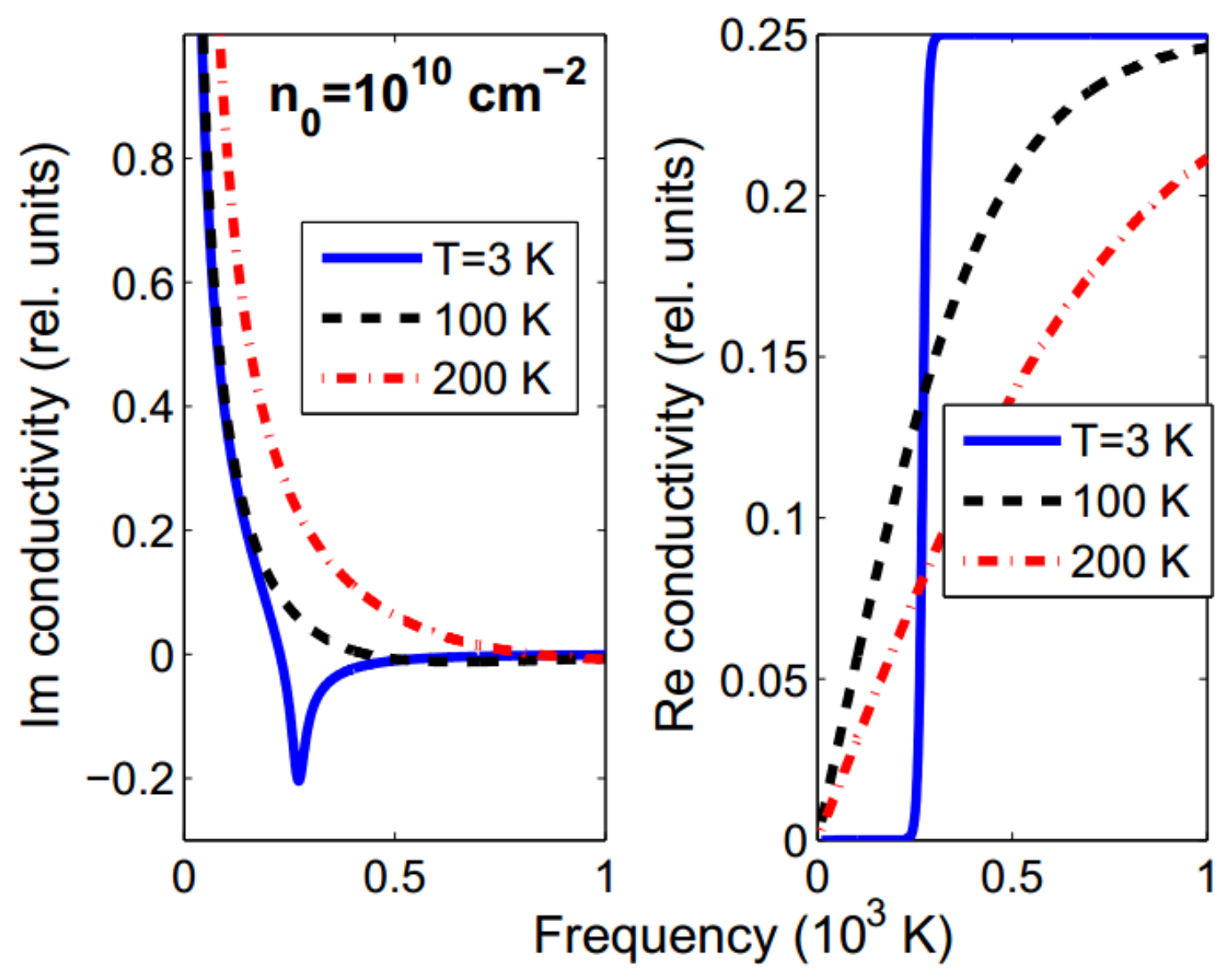
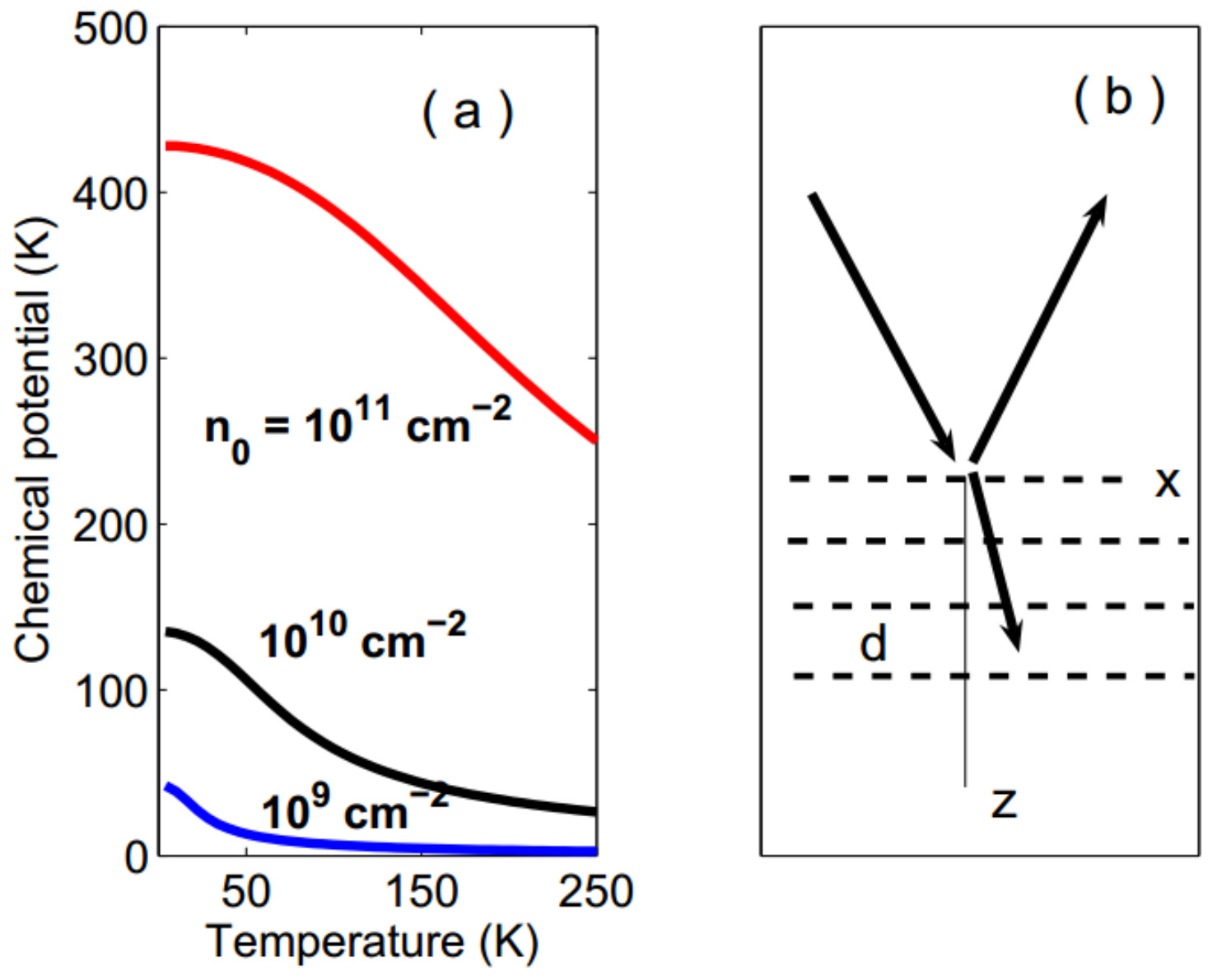
2.1. Optical Conductivity

The general expression for conductivity of graphene is discussed by Falkovsky et al. [24]. This dynamic conductivity of graphene (real and imaginary) is presented for observing the temperature and frequency relations by varying carrier concentration in both and multi-layers of graphene. It was discussed in the case of high frequencies considering ω > > ( k v , τ 1 ) ; here, dynamical conductivity is given by [24]
σ ( ω ) = e 2 i π [ + d ε ε ω 2 d f 0 ( ε ) d ε ] 0 + d ε f 0 ( ε ) f 0 ( ε ) ( ω + i δ ) 2 4 ε 2 ] ,
where f 0 ( ϵ ) = e x p [ ε μ T + 1 ] 1 is the Fermi function, ω is known as angular frequency, ε is the complex dielectric function, e indicates electron’s charge, τ 1 is defined as the rate of the collision of electron, v is considered velocity of Fermi level, k is considered wave vector, and ( ω + i δ ) is taken as the complex frequency. Equation (1) indicates the scattering process of electrons, and generally this phenomenon happens in the intraband stage. Integrating Equation (1)
σ i n t r a ( ω ) = 2 i e 2 T π ( ω + i τ 1 ) l n [ 2 c o s h ( μ 2 T ) ] ,
where μ is the chemical potential, and T indicates temperature. The term ( w + i τ 1 ) can be written instead of ω because the impurity process of the electron. Considering the Fermi–Dirac condition, the conductivity of the considered intraband is calculated through
σ i n t r a ( ω ) = 2 i e 2 T π ( ω + i τ 1 )
in the second part of Equation (1), where it is considered that δ is almost zero. In addition, considering the temperature is zero,
σ i n t r a ( ω ) = e 2 4 [ θ ( ω 2 μ ) i 2 π l n ( ω + 2 μ ) 2 ( ω 2 μ ) 2 ] .
In Equation (4), considering μ as positive, θ ( ω 2 μ ) is the electron absorption in the intraband in the case of low temperature. Taking the condition ω 2 μ and ω < μ , it can write from Equation (4)
θ ( ω 2 μ ) 1 2 + 1 π arctan θ ( ω 2 μ ) 2 T .
In the second integrate of Equation (1), the Fermi level can be written [24]
G ( ε ) = s i n h ( ε T ) c o s h ( μ T ) + c o s h ( ε T ) .
By operating on this equation using G ( ω / 2 ) , and also considering G ( ω / 2 ) = 0 , the interband conductivity can be written as
σ i n t e r ( ω ) = e 2 4 G ( ω 2 ) 4 ω i π 0 + d ε G ( ε ) G ( ω 2 ) ω 2 4 ε 2 .
Now, considering the Boltzmann and Fermi–Dirac, the first term of the equation can be written as [24]
G ( ω 2 ) = θ ( ω 2 μ ) , μ T , tanh ( ω 4 T ) , μ T .
Using Equations (2) and (7), the conductivity is calculated. In Figure 1, the real and imaginary parts are plotted when the temperature is low. The dotted black and red line present the characteristics if the temperature is increased. Conductivity unit is considered as e 2 for graphene doped. Generally, the conductivity is observed responsive for varying the frequency. However, low temperature like 3 K shows nonlinear behavior for both real and imaginary conductivity at 0.3 × 10 3 K frequency. At 0.5 × 10 3 K, the real value of conductivity is decreased by increasing temperature. Again, n 0 presents the electron density, and then chemical potential with the help of the electron density is calculated [24]
n 0 = 2 π ( v ) 2 0 + ε f 0 ( ε μ ) f 0 ( ε + μ ) d ε .
According to first figure, in Figure 2, there is a reverse relation between the temperature and chemical potential is observed.

2.2. Absorption, Transmission and Reflection Properties

In this section, optical transmission, reflection, and absorption of both mono layer and few layer graphene are represented by Kubo formula. This has been added dependence of optical conductivity of mono-layer graphene on chemical potential, temperature, frequency and relaxation time, both intraband and interband conductivity can be determined this using the Kubo formalism [26,27]
σ ( ω , μ c , τ , T ) = e 2 π 2 i ω i τ 1 i ( ω i τ 1 ) 2 0 ξ ξ f d ξ δ ξ ξ f d ξ δ ξ δ ξ 0 f d ξ f d ξ ω i τ 1 2 4 ξ 1 2 δ ξ .
Equation (10) consists of two parts, among them part 1 is considered as intraband and where part 2 is for interband. For having less complexity in intraband,
σ i n t r a ( ω , μ c , τ , T ) = e 2 π 2 i K B T ( ω i τ 1 ) μ c K B T + 2 ln e μ c K B T + 1 .
When μ c is greater than k B , then the interband contribution can be approximated like
σ i n t e r ( ω , μ c , τ , T ) = i e 2 4 π ln 2 μ c ( ω i τ 1 ) 2 μ c + ( ω i τ 1 ) .
Thus, the total conductivity of mono-layer graphene can be given by [28]
σ m o n o ( ω , μ c , τ , T ) = σ i n t r a ( ω , μ c , τ , T ) + σ i n t e r ( ω , μ c , τ , T ) .
Fermi–Dirac is expressed by [28]
f d ξ = 1 + e ξ μ c K B T 1 ,
where k B is the Boltzmann’s constant, and ξ is the Fermi energy, respectively. The use of few-layer graphene instead of mono-layer graphene is to reduce the thickness of the modulator. It is said that if the graphene has a small number of layers, then it shows the conductivity of the far infrared to the visible range [29,30,31,32]. For having this range, the optical conductivity of graphene of few layers can be written as [28]
σ f e w ( ω , μ c , τ , T ) = N σ m o n o ( ω , μ c , τ , T ) .
Using a matrix [28],
ε g r a p h e n e = ε g , t 0 0 0 ε g , t 0 0 0 ε g , t
can be written.
Graphene’s tangential permittivity can be given by [28]
ε g , t = 1 + j σ m o n o ( ω , μ c , τ , T ) ω ε 0 , t g m o n o ,
where mono-layer graphene’s thickness and permittivity of free space is defined by t g m o n o and ε 0 , respectively. To calculate the permittivity of graphene having small number of layers, it can be expressed as [28]
ε g f e w l a y e r = 1 + j σ f e w ( ω , μ c , τ , T ) ω ε 0 N t g m o n o .
Here, the thickness of few layer graphene is N times of mono layer, t g f e w = N t g m o n o . Moreover, the effective permittivity tensor of (few/mono-layer) graphene dielectric multilayer metamaterial with a unit cell thickness of d between 5 nm and 25 nm. For this, the specific frequency range of k 0 d < < 1 , where k 0 is the free space wave vector. Therefore, from effective medium theory (EMT), the effective permittivity tensor of the multilayer meta-material as [28]
ε e f f = ε l l 0 0 0 ε l l 0 0 0 ε l l ,
ε l l = f ε g , t + 1 f ε d ,
ε = f ε g , + 1 f ε d ,
where ε d is the dielectric permittivity and f is the fill fraction defined as [28]
f = t g t g + t d ,
where t d is considered as multilayer meta material cell thickness. Benefits of using few-layer graphene can be easily understood from the concept of fill fraction. However, both few-layer and mono-layer graphene permittivity have the same value, but the fill fraction for few-layer graphene dielectric multilayer meta-material is always higher than mono-layer. For a non-magnetic uni-axial meta-material, propagating wave vector for s and p polarization can be given by
k z s = ε 11 k 0 2 k x 2 ( f o r   s   p o l a r i z a t i o n ) ,
k z s = ε 11 k 0 2 ε 11 ε k x 2 ( f o r   p   p o l a r i z a t i o n ) .
Now, for an anisotropic meta-material slab with thickness d, total magnetic fields for Transverse Magnetic (TM) (p) polarized wave can be given by
H y i n c i d e n t m e d i a = H 0 e j k z + j k x + r p e j k z j k x ,
H y A m m m e d i a = H + e j k z p + j k x + H e j k z p j k x ,
H y e x i t m e d i a = t p e j k z + j k x ,
where k x = k 0 s i n θ and k z = k 0 c o s θ , θ is the incident angle, r p and t p are the complex amplitude coefficients of reflection and transmission of TM (p) wave by the slab, respectively. For Equations (25)–(27), there are four boundary conditions, and these conditions can be obtained by calculation of magnetic and electric field by varying the value of z ranging from 0 to d
r p = j p 1 p s i n k z z d 2 c o s k z p d + j ( p + 1 p ) s i n k z p d ,
r p = 2 2 c o s k z p + j p + 1 p s i n k z p d ,
where p = k x ε y k z p . For a Transverse Electric (TE) (s) polarized wave, reflection and transmission coefficients can also be expressed by Equations (28) and (29) with p replaced by, k x μ y k z s . From Equations (28) and (29), power transmission and reflection coefficients can be obtained as
T p = t p 2 ,
R p = r p 2 .
Absorption coefficient can be obtained as [28]
A s = 1 R s T s ( f o r   s   p o l a r i z a t i o n ) ,
A p = 1 R p T p ( f o r   p   p o l a r i z a t i o n ) .

2.3. Nonlinear Properties

Graphene contains nonlinear properties such as saturable absorption, multi-wave mixing, reverse saturable absorption, optical limiting, etc. These nonlinear properties are very much significant for the development of graphene-based devices [10]. From Figure 3, it is said that, due to the increase of intensity, there is a presence of reverse saturation absorption (RSA) in GO. In addition, the presence of organic materials provide the excited state absorption (ESA) and two photon absorption (2PA), which have the dominating process in nonlinear absorption [33]. In saturation absorption strategy, due to the increase of light, the absorption decreases. Because of these properties, a mechanism of electron transfer occurs, which leads a material to express its high attentive behavior. As graphene has no band gap, it can absorb the incident photons. If there is a high recombination rate of electron-hole gas, then the absorption does not take place in the excited state. As a result, the reverse process occurs. As shown in Figure 3, the absorption in different wavelengths are observed through the transient response. Moreover, graphene has another nonlinear property that is called multi-wave mixing. Sometimes, it is needed to mix the wave having different wavelengths. As shown in Figure 3, the two waves having different wavelengths are observed. Here, graphene can be used as an element for mixing the waves. Graphene also shows optical limiting property, in which there is a high transmittance rate despite having low intensity of light or vice versa.

2.4. Electrical Properties

The transparent conductor’s performance depends on the use of the ratio of absorption coefficient (visible range) and electrical conductivity. The absorption conductivity is defined as α and expressed electrical conductivity by σ [34]
σ α = 1 R s ln ( T + R ) ,
where R s expressed by sheet resistance ohm 2 , and T, R are expressed by transmission and reflection [35]. If the ratio becomes large, it then indicates good performance of the transparent conductor.

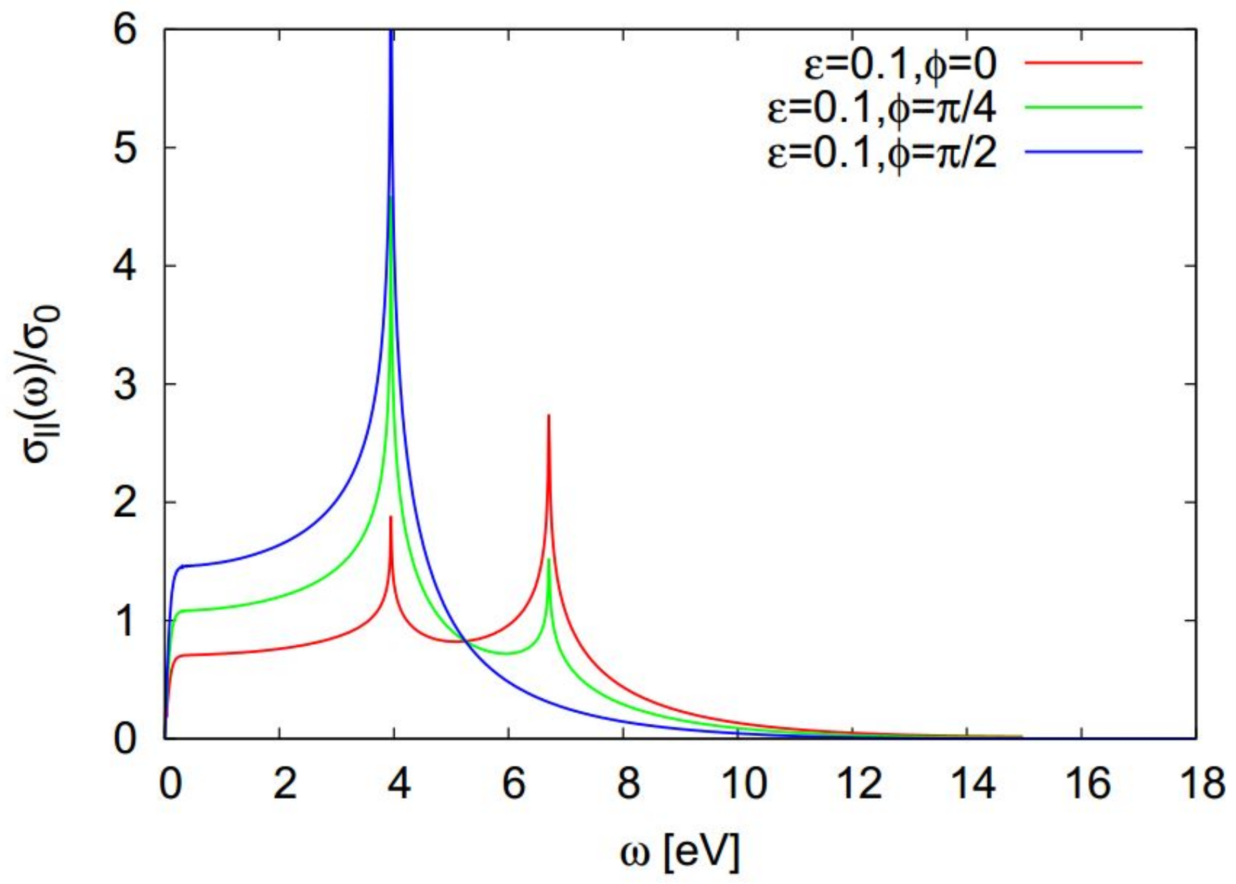
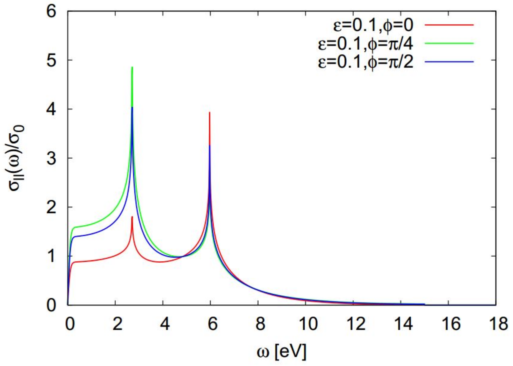
3. Optical Properties of Strained Graphene

Strain engineering has added a dynamic value in the optical properties of graphene. The anisotropic absorption caused by strain engineering added a new dimension for thin and transparent optical elements [36]. Guang-Xin et al. [36] showed that graphene transparency due to Polyethylene terephthalate (PET), in which there is a periodic modulation (0.1%), is seen as an effect of polarization direction. The term optical anisotropy caused by strain engineering is interpreted from that phenomena. The optical responses like reflection, transmission, and absorption are observed because of anisotropy, which is caused by strain [37]. Graphene is widely known as honeycomb lattice, in which each hexagonal structure is made of two triangular interpenetrating sub-lattices as shown in Figure 4. According to honeycomb lattice, graphene stays in s p 2 hybridization state. Low energy excitation can be observed in the honeycomb of graphene by electron hopping among the atoms. In the case of observing the modeling of graphene, the honeycomb lattice of graphene can be written as [37]
H = R t a ( R ) b ( R + δ ) + H . c . ,
where a ( R ) is an operator that is used to create the position R of a sub-lattice, and b ( R + δ ) is considered as a destruction operator for nearest neighbor (NN). ( R + δ ) and δ are considered as vector connectors for the nearest neighbors. t l t ( δ l ) , l = 1, 2, 3, where it is called the hopping parameter between NN sites. When there is no strain, then t t 0 , where t 0 = 2.8 eV [38]. The strain tensor can be represented as [39]
ϵ = ε c o s 2 θ v s i n 2 θ ( 1 + v ) c o s θ s i n θ ( 1 + v ) c o s θ s i n θ s i n 2 θ v c o s 2 θ .
Here, θ , ε and v = 0.14 are the applied strain angle, strain modulus and Poisson’s ratio.
In the case of optical conductivity, the density of current vector can be written as [38]
J ˜ ( P ) = e 2 m d P ( 2 π ) 2 ( 2 P + P ) c p c p + p .
In this equation, c p c p + p is treated as the destruction operator. In the case of homogeneous momentum (as the value of p is zero), the density of current vector can be written
J ˜ ( 0 ) = e i [ H , r ] = e r ,
where H is the Hamiltonian of the system. Now, considering linear-response theory, the conductivity σ can be related to the correlation of current–current function [38]
σ l m ( μ , T ; ω ) = i e 2 m ω δ i m + i ω N A c e l l Π ˜ l m R ( 0 , 0 , ω ) .
In this equation, N, T and ω are density of electron, temperature and external electric field, respectively. A c e l l , Π ˜ l m R ( 0 , 0 , ω ) are primitive cell area and current current correlation Fourier transform function. Considering the real part
σ l m ( μ , T ; ω ) = i ω N A c e l l l m Π ˜ l m R ( 0 , 0 , ω ) ,
now Π ˜ l m R can be written as [38]
Π ˜ l m ( P , P , τ ) = T τ J ˜ l ( P , τ ) J ˜ m ( P , 0 ) .
In this equation, J ˜ l ( P , τ ) is defined as the Fourier transform of current density vector and τ is the imaginary time. Now, using J ˜ l ( P , τ ) , it can be written as [38]
σ l m ( ω ) = R e 2 i A c e l l ω 1 N k λ J ˜ l ( k ) λ ¯ λ J ˜ m ( k ) λ ¯ λ n F ( ξ k λ ¯ ) n F ( ξ k λ ) ω + ξ k λ ξ k λ ¯ + i 0 + .
Here, ξ k λ = E k λ μ and n F ( ξ ) both are the Fermi function when the temperature is T. Now, in the case of external field, when, l = m , then
σ 11 ( ω ) σ 0 = 2 π τ 0 2 s i n h 1 2 β ω ω 1 N k λ J ˜ l ( k ) λ λ ¯ 2 F ( β , μ ; k ) δ ω ( E k λ E k λ ¯ ) ,
where β = ( k B T ) 1 is considered as inverse temperature, E K λ is band dispersion relation, λ = 1 , λ ¯ = 2 and β = ( k B T ) 1 is considered as inverse temperature. J ˜ l ( k ) = e t a J ˜ l ( k ) , σ 0 = π e 2 / ( 2 h ) is considered as quantum conductivity. In addition, τ 0 2 = 16 t 2 / ( 3 3 π 2 ) , and
F ( β , μ ; k ) = 2 e β ( E ¯ k μ ) n F ( ξ k , 1 ) n F ( ξ k , 2 ) ,
E ¯ k = E k , 1 + E k , 2 2 ,
having E ¯ k = 0 and g k = 0 (without overlap).
Here, Equation (43) represents the calculated longitude optical conductivity σ l l ( ω ) when frequency ω is greater than 0 having the temperature k B T = 0.025 eV. Figure 5 shows the strain applied result when θ is zero. In addition, the longitudinal optical conductivity is analyzed with the help of frequency ω and applied polar angle. When ε = 0 , then σ l l / σ o is found in isotropic condition because of the applied field angle and maximum frequency. The maximum frequency is split into distinct maxima when the strain modulus turns into non-zero. However, field direction ϕ plays a vital role in this phenomena.
In Figure 6, a plot of σ l l / σ 0 is shown when the strain modulus is ε = 0.1 and ϕ = 0 π / 2 . Relative weight of the shown maxima in the graph depends on their orientation among applied field and strain. Here, the value of μ is considered as zero. However, if there is a nonzero value of chemical potential is taken, then the result can be found with vanishing conductivity at ω = | μ | having a finite temperature effect.
Figure 7 indicates the strain applied optical conductivity and field orientation ratio considering frequency function.
These figures indicate the strain applied optical conductivity and field orientation ratio considering frequency function. The optical weight also depends on the relative orientation among applied field and strain. The last panel in Figure 7 shows large strain modulus (when ε = 0.275 ). In that case, there is an indication of the vanishing of optical conductivity as there is a gap is opened in the low energy sector of spectrum, which is indicated as a dark spot in the last part of Figure 7. In Figure 8 longitudinal optical conductivity is observed for different strain direction.

4. Applications of Graphene in Optoelectronics

4.1. Graphene in Mode-Locked Lasers

Due to having excellent electronic and mechanical properties, graphene is being used in micro and nano-chemical based systems such as transparent and thin-film transparent, conductive composites and so many. Mode-locking is a technique in which a saturable absorber (such as a nonlinear optical element) is used for the continuous laser output to ultra-short optical pulses. Semiconductor saturable absorber mirrors (SESAMs) are used generally in the case of mode-locking laser. The use of SESAM is complex in this case as it has complexity in fabrication and packaging [40,41]. This problem can be overcome by using graphene. Graphene has the characteristics of absorbing a good amount of incident light (2.3%) per layer [19]. Thus, comparing with SEASMs, graphene does not require band gap engineering or controlling diameter for achieving device performance. Sun et al. showed the use of an ultrafast mode-locked fiber laser at 1.5 m, which can be used in the field of optical telecommunication. Besides optical communication, these ultra-fast laser sources have various applied fields including basic research to medicine and material processing [42]. Researchers used graphene polymer composites, functionalism graphene such as graphene bonded with poly, reduced graphene oxide flakes, and CVD grown films for ultra-fast lasers [42,43]. In the case of optical communication, the integrated graphene can be placed in a predefined position such as fiber core or cavity mirror. In Figure 9, the integration of graphene is shown. Figure 9a indicates the transfer of integrated graphene into fiber cores. This movement can be done applying a water layer between the poly methyl methacrylate (PMMA)/graphene foil and optical fiber. A micromanipulator (Figure 9b) helps the target to place integrated graphene and the dissolution of the PMMA layer (Figure 9c). The most common strategy for integrating graphene saturable absorber (GSA) for pulse generation is sandwich GSA. In this case, a GSA in placed between two fiber connectors having a fiber adapter as shown in Figure 9d.

4.2. Application of Graphene as Photo-Detector

Photo detecting technology is blessed in the various modern applied fields like video imaging, bio-medical imaging, motion detection optical communication and so on. Due to the maturity of various high performing materials and integration of various technologies, the photo detection platform has become more efficient, secure and speedy compared with the past. Graphene has the property of a varying number of layers by tuning band-gap, which allows detection of light at various wavelengths. As a result, graphene can be used in ultra-fast technologies such as broadband communication, where general semiconductor based devices require strong absorption properties [45]. Graphene plays a vital role in optical communication as the bandwidth of the graphene based photo detector is measured as 262 GHz [46]. High-speed photo-detectors are also found in III–IV (>300) semiconductors, but there is a challenge to integrate with optic and electronic technologies [47]. Graphene has extra advantages characterizing of high speed modulation and detection on the same chip. According to [48], the graphene based photodetector shows outstanding results in detecting incident light as well as polarization on ultra-fast timescales. The performance of graphene based photodiodes, photoconductors and hybrid photo transistors are excellent as they have high photo-conductive gain because of their high mobility. As a result, the high voltage requirement is minimized and can be integrated simply with Si-based focal-plane arrays [49,50]. The photo current generated in graphene due to a photo thermometric effect plays a vital role in graphene based devices. An efficient photo current can be generated that has an electron-hole separation efficiency of more than 30% and an external electric field helps to produce it. Electrode–graphene interfaces can be helpful for zero-drain bias as well as dark current operations by using internal electric field [51].

4.3. Graphene Application in the Optical Modulator

Graphene has the characteristics of linear dispersion conduction and strong inter-band transition. It has excellent properties for photonic and optoelectronic applications. For example, it shows an ultra-fast response in the case of broadband light matter interaction. Using graphene’s Fermi level electrical tuning, the operation bandwidth of the graphene based optical modulator can be achieved as 1 GHz according to the response of electrical circuit [52]. The graphene based optical modulator can be used with gated graphene layer as it has a high refractive index wave guide when a thin oxide layer and Si operates as waveguide serves and gate electrode sequentially [53]. When heading to the application of bias voltage based on wave-guide and shifting of graphene layer, the Fermi energy is found around 0.3 eV, which blocks the inter-band transitions at a 1550 nm wavelength. A graphene based optical modulator can be used to enhance the quality factor as well as the resonance wavelength of cavity. Gan et al. used electro-optic modulation integrated with electrical gated mono-layer graphene to achieve the high performance [54]. Graphene has an extra advantage that it can be grown within a large area, which is very effective for electrically re-configurable devices. Polat et al. [55] used a graphene based optical modulator in which graphene based super capacitor was filled with liquid electrolyte, which shows a self-gating mechanism among graphene electrodes. In addition, the interesting part is that it does not require metallic gate electrodes. Being a very large electric field, the accumulated ions increase the carrier concentration of graphene electrodes. In Figure 10a, electrolyte gating is used to achieve a high level of doping, which confirms 70% absorption adaptability. Figure 10b represents a grapheme-dielectric based gating ring resonator. It shows fast switching at IR frequencies, while electrolyte gating provides slow operation in the visible spectrum. The significance of a wave-guide based optical modulator (Figure 10c) is to demonstrate a strong electro absorption modulation of 0.1 dB μ m 1 over a wide-band wavelength region [53].

4.4. Application of Graphene in Plasmonics

Graphene shows high quantum efficiency as well as optical nonlinear properties. Graphene can be modified for different types of applications using different ways such as gating, doping, chemical engineering and through conventional plasmonics. Plasmon in graphene provides an advantage over surface plasmon on a metal-dielectric interface by enabling strong confinement of electromagnetic energy at sub-wavelength scales. Graphene has added a new dimension in this field, as it has a linear band structure near the Dirac point. Moreover, the characteristics of graphene based highly doped THz plasmons depends on intra-band transitions of electrons. The surface plasmons (SPs) can also be excited through incident light. Using a high refractive index prism with SPs doped with mono-layer graphene can measure up to 10 THz [58]. Having these enhancement characteristics, THz SPs in graphene may be used in various rising applications like THz lasers, THz metamaterials, THz plasmonic antenna and so on [59]. A graphene mono-layer has the absorption of 2.3% slantwise from infrared (IR) to visible range because of its band arrangement, although this absorption can be changed by electrical gating. Moreover, the transverse magnetic (TM) mode plasmon can be controlled by electro absorption [60]. The highest loss of plasmon was obtained when there was a lower carrier concentration because of the enhancement of intraband absorption. With the help of this plasmonic modulator, more than 60 dB of on or off ratio can be observed. Graphene based plasmon plays a vital role in enhancing the properties of meta-materials. Results showed almost 250% enhancement of transmission at resonant frequency with the coverage of graphene. In addition, graphene can have an effect on meta-materials absorption and reflection properties at a specific frequency [59]. Raman spectroscopy can be used to analyze the structure of graphene, as it is a powerful technique that provides detailed information of the structure of a molecule. Microanalysis of different molecules can have an enlarge effect apart from graphene substrate, which is known as widely graphene enhanced Raman scattering (GERS). However, the enhancement effect is not strong enough, but due to the combination of graphene and metal nano particles, the effect can be improved [61,62].

4.5. Application of Graphene in Photonics

Graphene’s use in the field of photonics is growing. Because of its speedy performance, it has been considered for designing IC [63,64]. The photonic devices that are made using graphene show amazing reliable and speedy performance [65,66,67]. The absorption properties of graphene-related materials are also good. It can absorb only a small amount of the incident light (2–3%), and this absorption is almost the same for visible and UV light (universal optical conductivity) due to strong interaction between electrons and holes that form saddle point exciton and energy red shift [68,69,70,71,72]. As shown in Figure 11, the importance of using graphene in photonics is shown. The graphene plasmon can interact with polar insulator like substrates that are commonly used in SiO 2 . In this type, the surface photons generate a fluctuating electric field and it extends above the surface. As a result, hybrid modes of collective electrons (plasmon) and ionic lattice (phonon) excitation are generated [73,74]. This is used because of its excellent performance comparing silicon as well as (III–V) semiconductors. Its high conductivity is recorded as 36 times greater than Si and 100 times greater than GaAs. In addition, it has a superior optical threshold compared to Si and GaAs [75].

4.6. Application of Graphene in Optics

The optical communication system is going to a new high performing stage integrating silicon-based chips and designs with the help of graphene [76]. It is said that the leaders among blocks of photonic systems are optical modulators and photodetectors [11,77,78]. Graphene has a lot of applications in the field of optics. Graphene material, especially graphene nano-sheets, has applications in the field of synthesis, hybrids, molecular engineering, thin film, energy, etc. Nowadays, hybrid nano-structures contain at least one graphene nano-sheet (GN) and it has the properties of synergy that is induced by different nano scale objects. Mullen et al. [79] developed a bottom up approach to produce nano-sheets related to GN, which is shown in Figure 12.

4.7. Applications of Graphene in Sensing

Graphene is used in the sensing sector because of its excellent mechanical properties. which makes it easy for the fabrication process in nano electro mechanical system (NEMS) devices. Graphene can express its sensitiveness to operate in more than 150 MHz [81]. Table 1 shows some sensing related properties from which the use of graphene in sensing related fields is assumed [81].
As graphene has a zero band gap, it shows electric field effects. For this reason, charge that carries properties faces low effects though there is high temperature and a high concentration of electrons and holes [1,82,83]. Graphene can use the sensing application in the field of a transparent conductive field, clean energy devices, graphene–polymer nanocomposites, etc. Moreover, it can be applied to detect the oligonucleotides (single-stranded DNA, molecular beacons, and aptamers), proteins (thrombin), heavy metal ions (Ag), and pathogen (rota virus) [84,85,86,87]. Graphene materials also show electrochemical properties. In addition, it can be used to the detection of bio-macro molecules (DNA, hemoglobin, and α -fetoprotein), enzymes (horseradish peroxide and glucose oxidant), and small molecules (hydrogen peroxide, β -nicotinamide, adenine dinucleotide, dopamine and glucose) [88,89]. The electronic properties of it largely depend on chemical and atomic structures. In addition, the graphene material GO has optical properties of photoluminescence (PL) [90]. According to researchers, this property is useful for biosensing, fluorescence tags, and opto electronics applications [6,7,91,92]. Moreover, GO shows the characteristics of electron transfer due to its different electrical properties [93,94]. Electronic properties like conductivity of GO depends on atomic as well as chemical structure. Figure 13 represents the conductivity with respect to sp 2 fraction. Here a structural disorder of GO is observed because of the presence of a substantial carbon fraction. The two materials graphene and polycrystalline (PC) graphite used in this figure, are 100% sp 2 materials. Therefore, there are many application areas of graphene in sensing. Some of them are electro catalysts, electro-chemiluminescence, electrochemical gas sensors, electrochemical bio-sensors, electrochemical immunosensors, and electro-chemical DNA sensors. Graphene based material such as GO shows excellent optical properties as it shows the characteristics of a wide range of wavelengths ranging from near-infrared to ultraviolet [91]. Besides having been used in optical imaging, it is being used for quenching fluorescence. For having this excellent characteristics, GO can be used as an acceptor of fluorescence resonance energy transfer (FRET) as well as an energy donor. Graphene based sensors can also be used for sensitive fluorescent detection such as Pb 2 + [95]. Furthermore, graphene based gold nanoparticles was used to detect Pb 2 + in an aqueous solution [96].

4.8. Applications of Graphene in Mid-Infrared (MIR) Photonics

In the case of the plasmonic effect, graphene shows poor performance in visible wavelengths as well as near-IR. However, effective performance is found in MIR wavelengths [98]. Graphene can be useful for tunable MIR plasmonic related applied fields because some graphene related nano-structures like nano-disks or nano-ribbons can be helpful for electrostatic or chemical doping due to their low carrier concentration [99]. Wei et al. developed a pulsed laser operation that was mainly based on graphene, and it can operate at a wavelength close to 3 mm [100]. A group of researchers detects label-free protein mono-layers by using high sensitivity MIR plasmonic biosensor [101]. Photo-conductivity performance in graphene based material has been observed at different wavelengths. A research group found a wave-guide photodetector on a silicon-on-insulator (SOI) operating from a visible to MIR range [102]. High responsivity was found by them in the MIR (2.75 mm wavelength) range, and even the photonic energies are less compared with the Fermi level of p-doped graphene. According to this result, the graphene photo-detector has an MIR capability for optical detection in wavelengths. A graphene-on-silicon plasmonic-photonic Complementary metal–oxide–semiconductor (CMOS) compatible design was presented by Xiao et al. [103]. Results exhibited strong excitation of Graphene surface plasmon (GSP) by using a suspended membrane slot wave-guide. This design is helpful for inspecting an interaction process with the help of a wave-guides transmission spectrum, which can be applicable for the development of on chip electro-optical devices.

5. Applications of Graphene in Different Emerging Fields

5.1. Application of Graphene in Medical Science

This heavily-hyped material has the potential energy to rebirth our lives. It shows amazing performance in its miniature size. It is very helpful for various bio-medical related fields like cancer therapies, cancer detection, drug delivery, etc. Because of its unique properties like large surface area, having good chemical stability, and bio-compatibility, it has gained the attention of researchers. The distribution of size in graphene sheets indicates that it can vary from the nanometer to micrometer range. During the production of GO oxide, it shows the characteristics of different levels of impurities and dispensation. The details of application areas of graphene in medical fields are summarized in Table 2.

5.1.1. Graphene in Tissue Engineering

Kim et al. presented a model, which is useful for the tissue engineering. The effects of GO on various types of cells, and the effectiveness of GO for increasing the strength of bones is explained [116]. Graphene and its oxide can be used in different types of medical therapy. Pristine has the characteristics of cellular toxicity as macro-phage cells can be easily averted by surface functionalization [117]. Graphene has anti microbial applications. Different types of graphene-related materials, for example reduced graphene oxide (rGO), which has various types of effects on the bacterial model [118]. This research has given the bio-medical field a new dimension.

5.1.2. Graphene in Cancer Cell Detection

In medical diagnostic and therapeutic cases, graphene is used widely. It can work as direct cell detection. It used for both detecting cancer cells and the detection of rare pathological bacteria and pathogen [119,120]. In addition, graphene-based materials have excellent optical and electrochemical properties. It is used for constructing various types of cell-related bio-devices, which has good sensitivity [121]. These devices that are related to graphene have opened up a new dimension in the bio-medical field, with its eminent sensitive properties [107,122]. Sometimes, graphene is also used in cancer therapy. It can be used in the loading of chemotherapy drugs, vitro cancer cell targeting such as antibodies, peptide and folate acid, which shows good results under near-infrared light [6,123,124].

5.2. Other Graphene Applications

5.2.1. Application of Graphene in LED

For optical devices like LED fabrication, graphene is used because of its interaction with lattice giveing rise to new quasi particles. However, this phenomenon can happen at low energy with an effective speed of light ( 10 6 m 1 s 1 ). These electrons’ wave of the lattice has never failed to attract attention [125]. Graphene has applications in the field of electrodes in electrical and optical devices. This promising next generation material can replace the traditional material as it shows various electrical and mechanical characteristics. These high energetic optical properties are very effective in the use of LED related platforms as well as emerging revolution in the touch screen platform.
Optoelectronic based devices have gained much popularity and using widely. Various types of materials are used for the optoelectronic based devices. Among them, indium tin oxide (ITO) and fluorine tin oxide (FTO) are the most popular [126]. However, graphene can show better results than ITO or FTO. The experimental results are shown in Figure 9. Several research groups have reported that graphene has low sheet resistance and high transmittance to use them as transparent electrodes [127,128,129,130,131,132]. The opto-electric properties of graphene mainly depend on two significant considerations. One of them is sheet resistance, which deals the varying properties of sheets having various resistance. In addition, the other is light transmission, mainly the visible range. The aspect is that these two parameters have their own requirements. These properties can be changed to its desired values individually by changing the thickness of the graphene film. In touch screens, LEDs, and LCDs are now using graphene because of its mesmerizing characteristics. A graphene based touch screen can almost handle twin strains compared to conventional devices. Researchers have shown that the performance of prepared LCD using thermally thick GO has better results compared to traditional ITO-based devices [133]. In addition, graphene based LED has better performance compared to the featured ITO-based electrodes. Current ITO layers are superior to them in terms of electrical conductivity and transparency. However, flexibility can be introduced into transparent electrodes by incorporating graphene.
In the characteristics of transmittance, graphene shows tremendous results compared to ITO and FTO, which is shown in Figure 14. The experiment was done using a 1000 nm wavelength, having ca. 10 nm thickness. It shows the transmittance rate of 70.7% and the rate is lower than FTO, which has 82.4%. Almost having the same environment, the rate for ITO is recorded as 90%. The interesting part is that FTO and ITO show a strong absorption rate in near and short-wavelength (near 0.75 to 1.4 μ m, 1.4 to 3 μ m ). However, graphene stays transparent from the visible to MIR wavelength range [134].

5.2.2. Graphene in Solar Cells

The solar cell can work efficiently if it has the characteristics of high charge mobility and transport of holes or electrons through the materials. Graphene can be used in the solar cell as it includes those characteristics including high charge mobility as well as powerful light absorption capability [135,136], and increasing the number of graphene layers absorbs more power. In the organic solar cells, there is also the usage of graphene [134,137]. As window electrodes in the organic solar cell, graphene-based film of large poly-cyclic aromatic hydrocarbons was also employed. Arco et al. established high stretchy organic solar cell applying graphene electrodes [138]. Research shows that thermally reduced graphene has a transparency of 70% and conductivity of 550 S cm 1 . Having this result, graphene is used in dye-sensitized solar cells as window electrodes. Due to the use of graphene in solar cells, some excellent results are recorded as photo-current density (short-circuit) 1.01 mA cm 1 , voltage (open-circuit) 0.7 V, fill factor 0.36, and efficiency of power conversion is 0.26% [139].

5.2.3. Graphene as Field Effect Transistor (FET)

Graphene has a thin barrier that is used to inject charge. As a result, it has less resistance, which is helpful for activating channels in the optical field effect transistor (OFET). Graphene also can be used in molecular electronic devices as one of the most studied molecular junctions in the solid state device platform. In Figure 15a, a charging and discharging graph is shown. Figure 15b represents a peak variation due to various resistance. It is said that this property is helpful for analysis if industrial electro-optical related devices are used [140]. Research shows that the use of graphene material in BioFET has an impacts on certain molecules as micro molar sensitivity. It secures the advantages that there should not be a blockage for sensing related mechanisms [140].
In Figure 16, the optical properties based on gate are demonstrated. When the charge neutral point is +33, it indicates that the graphene is highly P-type. The transmission also depends on wavelength. The interference is measured from the silicon waveguide, just before the graphene layers are transferred. The wave-guide observed here has a high extinction ratio (>40 dB), having low optical loss (<0.1 dB). Moreover, the interference is calculated by applying different gate voltages. Results imply that the extinction ratio increased or decreased with the range of +40 V to −40 V. In addition, the excitation ratio and absorption coefficient in different gate voltages are presented. It is observed that the absorption coefficient can be modulated from 0.2 dB/ μ m having V g = + 33 V to 0.15 dB/ μ m when V g = 40 V. Moreover, the modulation depth of transmittance is found 64% [141].

5.2.4. Graphene in Fuel Cells

In the electrochemical chamber of a fuel cell, a chemical reaction like oxidation occurs to generate electricity. Graphene in that fuel chamber has a low impact on environment as it is an environmentally friendly high performing material [142].

6. Prospects and Aspects of Graphene

Graphene is well-known as a next generation material with many prospects and aspects for future development in the world. In addition, it is a tremendously diverse and attractive material in numerous aspects. Its research area is expanding quickly in the field of aeronautics, space research technology, clean energy, photo-catalysis, genetic engineering, intra-cellular imaging, amazing display technology, infrared imaging and so on [19,143]. Despite having so many features, graphene has some negative aspects. Researchers found that a negative Poisson’s ratio has an impact on room temperature [144]. It shows negative refraction in plasmon lensing [145]. Some nano composite fluids have malfunctioned due to graphene-related materials [146]. Therefore, a large number of fields include the applications of graphene from different perspectives. The properties of graphene are currently beyond imagination as many of its amazing characteristics are being incorporated day by day.

7. Conclusions

This 2D material has gained the focus of researchers since its appearance with its unique properties. In this review, the characteristics and applications of graphene and graphene-based materials in different fields like photonics, plasmonics, mode-locked lasers, optical modulators, photo-detectors, LED, medical diagnostic, optics, sensing, etc. are presented. The research and development of graphene-based devices are increasing rapidly. However, the research is still in the improvement phase and a large amount of work is required to appreciate graphene’s scientific prospects. It can be said that the applications in different fields can be quite competitive. Numerous other applications of graphene will be determined in the coming years, and achieving this will require continual, frequent, multidisciplinary research attempt and adequate financial support. Research on graphene is just beginning to ramp up, and this should bring up new phenomena.

Author Contributions

Himadri Shekhar Mondal and Md. Mahbub Hossain conceived and designed the analyzed, Md. Ekhlasur Rahaman, Sheikh Mohammed Boni Amin, Md. Bellal Hossain, Md. Mehadi Hasan Mahasin and Pankoj Kumar Mondal collected the data. Himadri Shekhar Mondal and Md. Mahbub Hossain wrote the paper.

Conflicts of Interest

The authors declare no conflict of interest.

References

  1. Novoselov, K.S.; Geim, A.K.; Morozov, S.V.; Jiang, D.; Zhang, Y.; Dubonos, S.V.; Grigorieva, I.V.; Firsov, A.A. Electric field effect in atomically thin carbon films. Science 2004, 306, 666–669. [Google Scholar] [CrossRef] [PubMed]
  2. Wassei, J.K.; Kaner, R.B. Graphene, a promising transparent conductor. Mater. Today 2010, 13, 52–59. [Google Scholar] [CrossRef]
  3. Hecht, D.S.; Hu, L.; Irvin, G. Emerging transparent electrodes based on thin films of carbon nanotubes, graphene, and metallic nanostructures. Adv. Mater. 2011, 23, 1482–1513. [Google Scholar] [CrossRef] [PubMed]
  4. Pang, S.; Hernandez, Y.; Feng, X.; Müllen, K. Graphene as transparent electrode material for organic electronics. Adv. Mater. 2011, 23, 2779–2795. [Google Scholar] [CrossRef] [PubMed]
  5. Liu, Z.; Robinson, J.T.; Sun, X.; Dai, H. PEGylated nanographene oxide for delivery of water-insoluble cancer drugs. J. Am. Chem. Soc. 2008, 130, 10876–10877. [Google Scholar] [CrossRef] [PubMed]
  6. Sun, X.; Liu, Z.; Welsher, K.; Robinson, J.T.; Goodwin, A.; Zaric, S.; Dai, H. Nano-graphene oxide for cellular imaging and drug delivery. Nano Res. 2008, 1, 203–212. [Google Scholar] [CrossRef] [PubMed]
  7. Liu, F.; Choi, J.Y.; Seo, T.S. Graphene oxide arrays for detecting specific DNA hybridization by fluorescence resonance energy transfer. Biosens. Bioelectr. 2010, 25, 2361–2365. [Google Scholar] [CrossRef] [PubMed]
  8. Dong, H.; Gao, W.; Yan, F.; Ji, H.; Ju, H. Fluorescence resonance energy transfer between quantum dots and graphene oxide for sensing biomolecules. Anal. Chem. 2010, 82, 5511–5517. [Google Scholar] [CrossRef] [PubMed]
  9. Wang, Y.; Li, Z.; Hu, D.; Lin, C.T.; Li, J.; Lin, Y. Aptamer/graphene oxide nanocomplex for in situ molecular probing in living cells. J. Am. Chem. Soc. 2010, 132, 9274–9276. [Google Scholar] [CrossRef] [PubMed]
  10. Liu, Z.; Zhang, X.; Yan, X.; Chen, Y.; Tian, J. Nonlinear optical properties of graphene-based materials. Chin. Sci. Bull. 2012, 57, 1–12. [Google Scholar] [CrossRef]
  11. Reed, G.T.; Mashanovich, G.; Gardes, F.; Thomson, D. Silicon optical modulators. Nat. Photonics 2010, 4, 518–526. [Google Scholar] [CrossRef] [Green Version]
  12. Wang, F.; Zhang, Y.; Tian, C.; Girit, C.; Zettl, A.; Crommie, M.; Shen, Y.R. Gate-variable optical transitions in graphene. Science 2008, 320, 206–209. [Google Scholar] [CrossRef] [PubMed]
  13. Liu, M.; Yin, X.; Zhang, X. Double-layer graphene optical modulator. Nano Lett. 2012, 12, 1482–1485. [Google Scholar] [CrossRef] [PubMed]
  14. Geim, A.K.; Novoselov, K.S. The rise of graphene. Nat. Mater. 2007, 6, 183–191. [Google Scholar] [CrossRef] [PubMed]
  15. Zhu, Y.; Murali, S.; Cai, W.; Li, X.; Suk, J.W.; Potts, J.R.; Ruoff, R.S. Graphene and graphene oxide: Synthesis, properties, and applications. Adv. Mater. 2010, 22, 3906–3924. [Google Scholar] [CrossRef] [PubMed]
  16. Balandin, A.A.; Ghosh, S.; Bao, W.; Calizo, I.; Teweldebrhan, D.; Miao, F.; Lau, C.N. Superior thermal conductivity of single-layer graphene. Nano Lett. 2008, 8, 902–907. [Google Scholar] [CrossRef] [PubMed]
  17. Chang, H.; Wu, H. Graphene-based nanomaterials: Synthesis, properties, and optical and optoelectronic applications. Adv. Funct. Mater. 2013, 23, 1984–1997. [Google Scholar] [CrossRef]
  18. Huang, X.; Yin, Z.; Wu, S.; Qi, X.; He, Q.; Zhang, Q.; Yan, Q.; Boey, F.; Zhang, H. Graphene-based materials: Synthesis, characterization, properties, and applications. Small 2011, 7, 1876–1902. [Google Scholar] [CrossRef] [PubMed]
  19. Nair, R.R.; Blake, P.; Grigorenko, A.N.; Novoselov, K.S.; Booth, T.J.; Stauber, T.; Peres, N.M.; Geim, A.K. Fine structure constant defines visual transparency of graphene. Science 2008, 320, 1308. [Google Scholar] [CrossRef] [PubMed]
  20. Kosynkin, D.V.; Higginbotham, A.L.; Sinitskii, A.; Lomeda, J.R.; Dimiev, A.; Price, B.K.; Tour, J.M. Longitudinal unzipping of carbon nanotubes to form graphene nanoribbons. Nature 2009, 458, 872. [Google Scholar] [CrossRef] [PubMed]
  21. Zhou, S.Y.; Gweon, G.H.; Fedorov, A.V.; First, P.N.; de Heer, W.A.; Lee, D.H.; Guinea, F.; Castro Neto, A.H.; Lanzara, A. Substrate-induced bandgap opening in epitaxial graphene. Nat. Mater. 2007, 6, 770–775. [Google Scholar] [CrossRef] [PubMed]
  22. Chang, H.; Sun, Z.; Yuan, Q.; Ding, F.; Tao, X.; Yan, F.; Zheng, Z. Thin Film Field-Effect Phototransistors from Bandgap-Tunable, Solution-Processed, Few-Layer Reduced Graphene Oxide Films. Adv. Mater. 2010, 22, 4872–4876. [Google Scholar] [CrossRef] [PubMed]
  23. Chang, H.; Cheng, J.; Liu, X.; Gao, J.; Li, M.; Li, J.; Tao, X.; Ding, F.; Zheng, Z. Facile Synthesis of Wide-Bandgap Fluorinated Graphene Semiconductors. Chem.-A Eur. J. 2011, 17, 8896–8903. [Google Scholar] [CrossRef] [PubMed]
  24. Falkovsky, L.; Varlamov, A. Space-time dispersion of graphene conductivity. Eur. Phys. J. B-Condens. Matter Complex Syst. 2007, 56, 281–284. [Google Scholar] [CrossRef]
  25. Falkovsky, L. Optical properties of graphene. J. Phys. Conf. Ser. IOP Publ. 2008, 129, 012004. [Google Scholar] [CrossRef]
  26. Hanson, G.W. Dyadic Green’s functions and guided surface waves for a surface conductivity model of graphene. J. Appl. Phys. 2008, 103, 064302. [Google Scholar] [CrossRef]
  27. Gusynin, V.; Sharapov, S.; Carbotte, J. Magneto-optical conductivity in graphene. J. Phys. Condens. Matter 2006, 19, 026222. [Google Scholar] [CrossRef]
  28. Al Sayem, A.; Mahdy, M.R.C.; Jahangir, I.; Rahman, M.S. Ultrathin ultra-broadband electro-absorption modulator based on few-layer graphene based anisotropic metamaterial. Opt. Commun. 2017, 384, 50–58. [Google Scholar] [CrossRef]
  29. Du, W.; Hao, R.; Li, E.P. The study of few-layer graphene based Mach- Zehnder modulator. Opt. Commun. 2014, 323, 49–53. [Google Scholar] [CrossRef]
  30. Min, H.; MacDonald, A.H. Origin of universal optical conductivity and optical stacking sequence identification in multilayer graphene. Phys. Rev. Lett. 2009, 103, 067402. [Google Scholar] [CrossRef] [PubMed]
  31. Ya-Qin, C. Determination of the in-plane optical conductivity of multilayer graphene supported on a transparent substrate of finite thickness from normal-incidence transmission spectra. Chin. Phys. Lett. 2014, 31, 057802. [Google Scholar]
  32. Mak, K.F.; Sfeir, M.Y.; Misewich, J.A.; Heinz, T.F. The evolution of electronic structure in few-layer graphene revealed by optical spectroscopy. Proc. Natl. Acad. Sci. USA 2010, 107, 14999–15004. [Google Scholar] [CrossRef] [PubMed]
  33. Biswas, S.; Kole, A.; Tiwary, C.; Kumbhakar, P. Enhanced nonlinear optical properties of graphene oxide–silver nanocomposites measured by Z-scan technique. RSC Adv. 2016, 6, 10319–10325. [Google Scholar] [CrossRef]
  34. Jo, G.; Choe, M.; Lee, S.; Park, W.; Kahng, Y.H.; Lee, T. The application of graphene as electrodes in electrical and optical devices. Nanotechnology 2012, 23, 112001. [Google Scholar] [CrossRef] [PubMed]
  35. Gordon, R.G. Criteria for choosing transparent conductors. MRS bulletin 2000, 25, 52–57. [Google Scholar] [CrossRef]
  36. Ni, G.X.; Yang, H.Z.; Ji, W.; Baeck, S.J.; Toh, C.T.; Ahn, J.H.; Pereira, V.M.; Özyilmaz, B. Tuning Optical Conductivity of Large-Scale CVD Graphene by Strain Engineering. Adv. Mater. 2014, 26, 1081–1086. [Google Scholar] [CrossRef] [PubMed]
  37. Pereira, V.M.; Ribeiro, R.; Peres, N.; Neto, A.C. Optical properties of strained graphene. EPL (Europhys. Lett.) 2011, 92, 67001. [Google Scholar] [CrossRef]
  38. Pellegrino, F.; Angilella, G.; Pucci, R. Strain effect on the optical conductivity of graphene. Phys. Rev. B 2010, 81, 035411. [Google Scholar] [CrossRef]
  39. Pereira, V.M.; Neto, A.C.; Peres, N. Tight-binding approach to uniaxial strain in graphene. Phys. Rev. B 2009, 80, 045401. [Google Scholar] [CrossRef]
  40. Hasan, T.; Sun, Z.; Wang, F.; Bonaccorso, F.; Tan, P.H.; Rozhin, A.G.; Ferrari, A.C. Nanotube–polymer composites for ultrafast photonics. Adv. Mater. 2009, 21, 3874–3899. [Google Scholar] [CrossRef]
  41. Keller, U. Recent developments in compact ultrafast lasers. Nature 2003, 424, 831. [Google Scholar] [CrossRef] [PubMed]
  42. Sun, Z.; Hasan, T.; Torrisi, F.; Popa, D.; Privitera, G.; Wang, F.; Bonaccorso, F.; Basko, D.M.; Ferrari, A.C. Graphene mode-locked ultrafast laser. ACS Nano 2010, 4, 803–810. [Google Scholar] [CrossRef] [PubMed]
  43. Bao, Q.; Zhang, H.; Wang, Y.; Ni, Z.; Yan, Y.; Shen, Z.X.; Loh, K.P.; Tang, D.Y. Atomic-layer graphene as a saturable absorber for ultrafast pulsed lasers. Adv. Funct. Mater. 2009, 19, 3077–3083. [Google Scholar] [CrossRef]
  44. Bonaccorso, F.; Sun, Z.; Hasan, T.; Ferrari, A. Graphene photonics and optoelectronics. Nat. Photonics 2010, 4, 611–622. [Google Scholar] [CrossRef]
  45. Koppens, F.; Mueller, T.; Avouris, P.; Ferrari, A.; Vitiello, M.; Polini, M. Photodetectors based on graphene, other two-dimensional materials and hybrid systems. Nat. Nanotechnol. 2014, 9, 780–793. [Google Scholar] [CrossRef] [PubMed]
  46. Urich, A.; Unterrainer, K.; Mueller, T. Intrinsic response time of graphene photodetectors. Nano Lett. 2011, 11, 2804–2808. [Google Scholar] [CrossRef] [PubMed]
  47. Ito, H.; Furuta, T.; Kodama, S.; Watanabe, N.; Ishibashi, T. InP/InGaAs uni-travelling-carrier photodiode with 220 GHz bandwidth. Electron. Lett. 1999, 35, 1556–1557. [Google Scholar] [CrossRef]
  48. Echtermeyer, T.J.; Nene, P.; Trushin, M.; Gorbachev, R.V.; Eiden, A.L.; Milana, S.; Sun, Z.; Schliemann, J.; Lidorikis, E.; Novoselov, K.S.; et al. Photothermoelectric and photoelectric contributions to light detection in metal–graphene–metal photodetectors. Nano Lett. 2014, 14, 3733–3742. [Google Scholar] [CrossRef] [PubMed]
  49. Sun, Z.; Liu, Z.; Li, J.; Tai, G.a.; Lau, S.P.; Yan, F. Infrared photodetectors based on CVD-grown graphene and PbS quantum dots with ultrahigh responsivity. Adv. Mater. 2012, 24, 5878–5883. [Google Scholar] [CrossRef] [PubMed]
  50. Konstantatos, G.; Badioli, M.; Gaudreau, L.; Osmond, J.; Bernechea, M.; De Arquer, F.P.G.; Gatti, F.; Koppens, F.H. Hybrid graphene–quantum dot phototransistors with ultrahigh gain. Nat. Nanotechnol. 2012, 7, 363. [Google Scholar] [CrossRef] [PubMed]
  51. Park, J.; Ahn, Y.; Ruiz-Vargas, C. Imaging of photocurrent generation and collection in single-layer graphene. Nano Lett. 2009, 9, 1742–1746. [Google Scholar] [CrossRef] [PubMed]
  52. Li, W.; Chen, B.; Meng, C.; Fang, W.; Xiao, Y.; Li, X.; Hu, Z.; Xu, Y.; Tong, L.; Wang, H.; et al. Ultrafast all-optical graphene modulator. Nano Lett. 2014, 14, 955–959. [Google Scholar] [CrossRef] [PubMed]
  53. Liu, M.; Yin, X.; Ulin-Avila, E.; Geng, B.; Zentgraf, T.; Ju, L.; Wang, F.; Zhang, X. A graphene-based broadband optical modulator. Nature 2011, 474, 64–67. [Google Scholar] [CrossRef] [PubMed]
  54. Gan, X.; Shiue, R.J.; Gao, Y.; Mak, K.F.; Yao, X.; Li, L.; Szep, A.; Walker Jr, D.; Hone, J.; Heinz, T.F.; et al. High-contrast electrooptic modulation of a photonic crystal nanocavity by electrical gating of graphene. Nano Lett. 2013, 13, 691–696. [Google Scholar] [CrossRef] [PubMed]
  55. Polat, E.O.; Kocabas, C. Broadband optical modulators based on graphene supercapacitors. Nano Lett. 2013, 13, 5851–5857. [Google Scholar] [CrossRef] [PubMed] [Green Version]
  56. Lee, E.J.; Choi, S.Y.; Jeong, H.; Park, N.H.; Yim, W.; Kim, M.H.; Park, J.K.; Son, S.; Bae, S.; Kim, S.J.; et al. Active control of all-fibre graphene devices with electrical gating. Nat. Commun. 2015, 6, 6851. [Google Scholar] [CrossRef] [PubMed]
  57. Phare, C.T.; Lee, Y.H.D.; Cardenas, J.; Lipson, M. Graphene electro-optic modulator with 30 GHz bandwidth. Nat. Photonics 2015, 9, 511–514. [Google Scholar] [CrossRef]
  58. How Gan, C. Analysis of surface plasmon excitation at terahertz frequencies with highly doped graphene sheets via attenuated total reflection. Appl. Phys. Lett. 2012, 101, 111609. [Google Scholar] [CrossRef]
  59. Luo, X.; Qiu, T.; Lu, W.; Ni, Z. Plasmons in graphene: Recent progress and applications. Mater. Sci. Eng. R Rep. 2013, 74, 351–376. [Google Scholar] [CrossRef]
  60. Andersen, D.R. Graphene-based long-wave infrared TM surface plasmon modulator. JOSAB 2010, 27, 818–823. [Google Scholar] [CrossRef]
  61. Xu, W.; Ling, X.; Xiao, J.; Dresselhaus, M.S.; Kong, J.; Xu, H.; Liu, Z.; Zhang, J. Surface enhanced Raman spectroscopy on a flat graphene surface. Proc. Natl. Acad. Sci. USA 2012, 109, 9281–9286. [Google Scholar] [CrossRef] [PubMed]
  62. Niu, J.; Truong, V.G.; Huang, H.; Tripathy, S.; Qiu, C.; Wee, A.T.; Yu, T.; Yang, H. Study of electromagnetic enhancement for surface enhanced Raman spectroscopy of SiC graphene. Appl. Phys. Lett. 2012, 100, 191601. [Google Scholar] [CrossRef]
  63. Bolotin, K.I.; Sikes, K.; Jiang, Z.; Klima, M.; Fudenberg, G.; Hone, J.; Kim, P.; Stormer, H. Ultrahigh electron mobility in suspended graphene. Solid State Commun. 2008, 146, 351–355. [Google Scholar] [CrossRef]
  64. Avouris, P.; Chen, Z.; Perebeinos, V. Carbon-based electronics. Nat. Nanotechnol. 2007, 2, 605–615. [Google Scholar] [CrossRef] [PubMed]
  65. Chen, P.Y.; Alù, A. Atomically thin surface cloak using graphene monolayers. ACS Nano 2011, 5, 5855–5863. [Google Scholar] [CrossRef] [PubMed]
  66. Vakil, A.; Engheta, N. Transformation optics using graphene. Science 2011, 332, 1291–1294. [Google Scholar] [CrossRef] [PubMed]
  67. Ju, L.; Geng, B.; Horng, J.; Girit, C.; Martin, M.; Hao, Z.; Bechtel, H.A.; Liang, X.; Zettl, A.; Shen, Y.R.; et al. Graphene plasmonics for tunable terahertz metamaterials. Nat. Nanotechnol. 2011, 6, 630–634. [Google Scholar] [CrossRef] [PubMed]
  68. He, S.; Song, B.; Li, D.; Zhu, C.; Qi, W.; Wen, Y.; Wang, L.; Song, S.; Fang, H.; Fan, C. A graphene nanoprobe for rapid, sensitive, and multicolor fluorescent DNA analysis. Adv. Funct. Mater. 2010, 20, 453–459. [Google Scholar] [CrossRef]
  69. Sun, Z.; Popa, D.; Hasan, T.; Torrisi, F.; Wang, F.; Kelleher, E.J.; Travers, J.C.; Nicolosi, V.; Ferrari, A.C. A stable, wideband tunable, near transform-limited, graphene-mode-locked, ultrafast laser. Nano Res. 2010, 3, 653–660. [Google Scholar] [CrossRef]
  70. Bao, Q.; Zhang, H.; Wang, B.; Ni, Z.; Lim, C.H.Y.X.; Wang, Y.; Tang, D.Y.; Loh, K.P. Broadband graphene polarizer. Nat. Photonics 2011, 5, 411–415. [Google Scholar] [CrossRef]
  71. Mueller, T.; Xia, F.; Avouris, P. Graphene photodetectors for high-speed optical communications. Nat. Photonics 2010, 4, 297–301. [Google Scholar] [CrossRef]
  72. Xia, F.; Mueller, T.; Lin, Y.M.; Valdes-Garcia, A.; Avouris, P. Ultrafast graphene photodetector. Nat. Nanotechnol. 2009, 4, 839–843. [Google Scholar] [CrossRef] [PubMed]
  73. Fischetti, M.V.; Neumayer, D.A.; Cartier, E.A. Effective electron mobility in Si inversion layers in metal–oxide– semiconductor systems with a high-κ insulator: The role of remote phonon scattering. J. Appl. Phys. 2001, 90, 4587–4608. [Google Scholar] [CrossRef]
  74. Freitag, M.; Low, T.; Zhu, W.; Yan, H.; Xia, F.; Avouris, P. Photocurrent in graphene harnessed by tunable intrinsic plasmons. Nat. Commun. 2013. [Google Scholar] [CrossRef] [PubMed]
  75. Bao, Q.; Loh, K.P. Graphene photonics, plasmonics, and broadband optoelectronic devices. ACS Nano 2012, 6, 3677–3694. [Google Scholar] [CrossRef] [PubMed]
  76. Vlasov, Y.A. Silicon CMOS-integrated nano-photonics for computer and data communications beyond 100 G. IEEE Commun. Mag. 2012, 50. [Google Scholar] [CrossRef]
  77. Koester, S.J.; Schaub, J.D.; Dehlinger, G.; Chu, J.O. Germanium-on-SOI infrared detectors for integrated photonic applications. IEEE J. Sel. Top. Quantum Electron. 2006, 12, 1489–1502. [Google Scholar] [CrossRef]
  78. Assefa, S.; Xia, F.; Vlasov, Y.A. Reinventing germanium avalanche photodetector for nanophotonic on-chip optical interconnects. Nature 2010, 464, 80. [Google Scholar] [CrossRef] [PubMed]
  79. Mullen, E.M. Mullen Scales of Early Learning; AGS Circle Pines: Minneapolis, MN, USA, 1995. [Google Scholar]
  80. Yang, S.; Feng, X.; Wang, L.; Tang, K.; Maier, J.; Müllen, K. Graphene-Based Nanosheets with a Sandwich Structure. Angew. Chem. Int. Ed. 2010, 49, 4795–4799. [Google Scholar] [CrossRef] [PubMed]
  81. Bogue, R. Graphene sensors: A review of recent developments. Sens. Rev. 2014, 34, 233–238. [Google Scholar] [CrossRef]
  82. Novoselov, K.S.; Geim, A.K.; Morozov, S.; Jiang, D.; Katsnelson, M.; Grigorieva, I.; Dubonos, S.; Firsov, A.A. Two-dimensional gas of massless Dirac Fermions in graphene. Nature 2005, 438, 197–200. [Google Scholar] [CrossRef] [PubMed] [Green Version]
  83. Zhang, Y.; Tan, Y.W.; Stormer, H.L.; Kim, P. Experimental observation of quantum Hall effect and Berry’s phase in graphene. Nature 2005, 438, 201–204. [Google Scholar] [CrossRef] [PubMed]
  84. Jung, J.H.; Cheon, D.S.; Liu, F.; Lee, K.B.; Seo, T.S. A graphene oxide based immuno-biosensor for pathogen detection. Angew. Chem. Int. Ed. 2010, 49, 5708–5711. [Google Scholar] [CrossRef] [PubMed]
  85. Lu, C.H.; Yang, H.H.; Zhu, C.L.; Chen, X.; Chen, G.N. A graphene platform for sensing biomolecules. Angew. Chem. 2009, 121, 4879–4881. [Google Scholar] [CrossRef]
  86. Chang, H.; Tang, L.; Wang, Y.; Jiang, J.; Li, J. Graphene fluorescence resonance energy transfer aptasensor for the thrombin detection. Anal. Chem. 2010, 82, 2341–2346. [Google Scholar] [CrossRef] [PubMed]
  87. Li, F.; Huang, Y.; Yang, Q.; Zhong, Z.; Li, D.; Wang, L.; Song, S.; Fan, C. A graphene-enhanced molecular beacon for homogeneous DNA detection. Nanoscale 2010, 2, 1021–1026. [Google Scholar] [CrossRef] [PubMed]
  88. Zhou, M.; Zhai, Y.; Dong, S. Electrochemical sensing and biosensing platform based on chemically reduced graphene oxide. Anal. Chem. 2009, 81, 5603–5613. [Google Scholar] [CrossRef] [PubMed]
  89. Xu, C.; Wang, X.; Wang, J.; Hu, H.; Wan, L. Synthesis and photoelectrical properties of β-cyclodextrin functionalized graphene materials with high bio-recognition capability. Chem. Phys. Lett. 2010, 498, 162–167. [Google Scholar] [CrossRef]
  90. Loh, K.P.; Bao, Q.; Eda, G.; Chhowalla, M. Graphene oxide as a chemically tunable platform for optical applications. Nat. Chem. 2010, 2, 1015–1024. [Google Scholar] [CrossRef] [PubMed]
  91. Luo, Z.; Vora, P.M.; Mele, E.J.; Johnson, A.C.; Kikkawa, J.M. Photoluminescence and band gap modulation in graphene oxide. Appl. Phys. Lett. 2009, 94, 111909. [Google Scholar] [CrossRef]
  92. Eda, G.; Lin, Y.Y.; Mattevi, C.; Yamaguchi, H.; Chen, H.A.; Chen, I.; Chen, C.W.; Chhowalla, M. Blue photoluminescence from chemically derived graphene oxide. Adv. Mater. 2010, 22, 505–509. [Google Scholar] [CrossRef] [PubMed]
  93. Liu, H.; Gao, J.; Xue, M.; Zhu, N.; Zhang, M.; Cao, T. Processing of graphene for electrochemical application: Noncovalently functionalize graphene sheets with water-soluble electroactive methylene green. Langmuir 2009, 25, 12006–12010. [Google Scholar] [CrossRef] [PubMed]
  94. Wang, Z.; Zhou, X.; Zhang, J.; Boey, F.; Zhang, H. Direct electrochemical reduction of single-layer graphene oxide and subsequent functionalization with glucose oxidase. J. Phys. Chem. C 2009, 113, 14071–14075. [Google Scholar] [CrossRef]
  95. Zhao, X.H.; Kong, R.M.; Zhang, X.B.; Meng, H.M.; Liu, W.N.; Tan, W.; Shen, G.L.; Yu, R.Q. Graphene– DNAzyme based biosensor for amplified fluorescence “turn-on” detection of Pb2+ with a high selectivity. Anal. Chem. 2011, 83, 5062–5066. [Google Scholar] [CrossRef] [PubMed]
  96. Fu, X.; Lou, T.; Chen, Z.; Lin, M.; Feng, W.; Chen, L. “Turn-on” fluorescence detection of lead ions based on accelerated leaching of gold nanoparticles on the surface of graphene. ACS Appl. Mater. Interfaces 2012, 4, 1080–1086. [Google Scholar] [CrossRef] [PubMed]
  97. Chen, D.; Feng, H.; Li, J. Graphene oxide: Preparation, functionalization, and electrochemical applications. Chem. Rev. 2012, 112, 6027–6053. [Google Scholar] [CrossRef] [PubMed]
  98. Yan, H.; Low, T.; Zhu, W.; Wu, Y.; Freitag, M.; Li, X.; Guinea, F.; Avouris, P.; Xia, F. Damping pathways of mid-infrared plasmons in graphene nanostructures. Nat. Photonics 2013, 7, 394–399. [Google Scholar] [CrossRef]
  99. Cheng, Z.; Qin, C.; Wang, F.; He, H.; Goda, K. Progress on mid-IR graphene photonics and biochemical applications. Front. Optoelectron. 2016, 9, 259–269. [Google Scholar] [CrossRef]
  100. Wei, C.; Zhu, X.; Wang, F.; Xu, Y.; Balakrishnan, K.; Song, F.; Norwood, R.A.; Peyghambarian, N. Graphene Q-switched 2.78 μm Er 3+-doped fluoride fiber laser. Opt. Lett. 2013, 38, 3233–3236. [Google Scholar] [CrossRef] [PubMed]
  101. Rodrigo, D.; Limaj, O.; Janner, D.; Etezadi, D.; de Abajo, F.J.G.; Pruneri, V.; Altug, H. Mid-infrared plasmonic biosensing with graphene. Science 2015, 349, 165–168. [Google Scholar] [CrossRef] [PubMed]
  102. Wang, X.; Cheng, Z.; Xu, K.; Tsang, H.K.; Xu, J.B. High-responsivity graphene/silicon-heterostructure waveguide photodetectors. Nat. Photonics 2013, 7, 888. [Google Scholar] [CrossRef]
  103. Xiao, T.H.; Cheng, Z.; Goda, K. Graphene-on-silicon hybrid plasmonic-photonic integrated circuits. Nanotechnology 2017, 28, 245201. [Google Scholar] [CrossRef] [PubMed]
  104. Liu, Y.; Yu, D.; Zeng, C.; Miao, Z.; Dai, L. Biocompatible graphene oxide-based glucose biosensors. Langmuir 2010, 26, 6158–6160. [Google Scholar] [CrossRef] [PubMed]
  105. Li, F.; Feng, Y.; Zhao, C.; Li, P.; Tang, B. A sensitive graphene oxide–DNA based sensing platform for fluorescence “turn-on” detection of bleomycin. Chem. Commun. 2012, 48, 127–129. [Google Scholar] [CrossRef] [PubMed]
  106. Giovanni, M.; Bonanni, A.; Pumera, M. Detection of DNA hybridization on chemically modified graphene platforms. Analyst 2012, 137, 580–583. [Google Scholar] [CrossRef] [PubMed]
  107. Wang, H.; Zhang, Q.; Chu, X.; Chen, T.; Ge, J.; Yu, R. Graphene oxide–peptide conjugate as an intracellular protease sensor for caspase-3 activation imaging in live cells. Angew. Chem. Int. Ed. 2011, 50, 7065–7069. [Google Scholar] [CrossRef] [PubMed]
  108. Wang, Y.; Xiao, Y.; Ma, X.; Li, N.; Yang, X. Label-free and sensitive thrombin sensing on a molecularly grafted aptamer on graphene. Chem. Commun. 2012, 48, 738–740. [Google Scholar] [CrossRef] [PubMed]
  109. Li, L.; Chen, M.; Zhang, H.; Nie, H.; Sun, J.Z.; Qin, A.; Tang, B.Z. Influence of the number and substitution position of phenyl groups on the aggregation-enhanced emission of benzene-cored luminogens. Chem. Commun. 2015, 51, 4830–4833. [Google Scholar] [CrossRef] [PubMed]
  110. Wang, H.; Chen, T.; Wu, S.; Chu, X.; Yu, R. A novel biosensing strategy for screening G-quadruplex ligands based on graphene oxide sheets. Biosens. Bioelectron. 2012, 34, 88–93. [Google Scholar] [CrossRef] [PubMed]
  111. Lee, J.; Min, D.H. A simple fluorometric assay for DNA exonuclease activity based on graphene oxide. Analyst 2012, 137, 2024–2026. [Google Scholar] [CrossRef] [PubMed]
  112. Bitounis, D.; Ali-Boucetta, H.; Hong, B.H.; Min, D.H.; Kostarelos, K. Prospects and challenges of graphene in biomedical applications. Adv. Mater. 2013, 25, 2258–2268. [Google Scholar] [CrossRef] [PubMed]
  113. Ruan, C.; Li, T.; Niu, Q.; Lu, M.; Lou, J.; Gao, W.; Sun, W. Electrochemical myoglobin biosensor based on graphene–ionic liquid–chitosan bionanocomposites: Direct electrochemistry and electrocatalysis. Electrochim. Acta 2012, 64, 183–189. [Google Scholar] [CrossRef]
  114. Li, X.; Chen, M.; Ma, X. Selective determination of epinephrine in the presence of ascorbic acid using a glassy carbon electrode modified with graphene. Anal. Sci. 2012, 28, 147–151. [Google Scholar] [CrossRef] [PubMed]
  115. Feng, L.; Chen, Y.; Ren, J.; Qu, X. A graphene functionalized electrochemical aptasensor for selective label-free detection of cancer cells. Biomaterials 2011, 32, 2930–2937. [Google Scholar] [CrossRef] [PubMed]
  116. Kim, S.; Ku, S.H.; Lim, S.Y.; Kim, J.H.; Park, C.B. Graphene–biomineral hybrid materials. Adv. Mater. 2011, 23, 2009–2014. [Google Scholar] [CrossRef] [PubMed]
  117. Singh, S.K.; Singh, M.K.; Nayak, M.K.; Kumari, S.; Shrivastava, S.; Grácio, J.J.; Dash, D. Thrombus inducing property of atomically thin graphene oxide sheets. ACS Nano 2011, 5, 4987–4996. [Google Scholar] [CrossRef] [PubMed]
  118. Liu, S.; Zeng, T.H.; Hofmann, M.; Burcombe, E.; Wei, J.; Jiang, R.; Kong, J.; Chen, Y. Antibacterial activity of graphite, graphite oxide, graphene oxide, and reduced graphene oxide: Membrane and oxidative stress. ACS Nano 2011, 5, 6971–6980. [Google Scholar] [CrossRef] [PubMed]
  119. Mohanty, N.; Berry, V. Graphene-based single-bacterium resolution biodevice and DNA transistor: Interfacing graphene derivatives with nanoscale and microscale biocomponents. Nano Lett. 2008, 8, 4469–4476. [Google Scholar] [CrossRef] [PubMed]
  120. Zelada-Guillén, G.A.; Riu, J.; Düzgün, A.; Rius, F.X. Immediate detection of living bacteria at ultralow concentrations using a carbon nanotube based potentiometric aptasensor. Angew. Chem. Int. Ed. 2009, 48, 7334–7337. [Google Scholar] [CrossRef] [PubMed]
  121. Kempaiah, R.; Chung, A.; Maheshwari, V. Graphene as cellular interface: Electromechanical coupling with cells. ACS Nano 2011, 5, 6025–6031. [Google Scholar] [CrossRef] [PubMed]
  122. Jang, H.; Kim, Y.K.; Kwon, H.M.; Yeo, W.S.; Kim, D.E.; Min, D.H. A Graphene-Based Platform for the Assay of Duplex-DNA Unwinding by Helicase. Angew. Chem. 2010, 122, 5839–5843. [Google Scholar] [CrossRef]
  123. Yang, X.; Wang, Y.; Huang, X.; Ma, Y.; Huang, Y.; Yang, R.; Duan, H.; Chen, Y. Multi-functionalized graphene oxide based anticancer drug-carrier with dual-targeting function and pH-sensitivity. J. Mater. Chem. 2011, 21, 3448–3454. [Google Scholar] [CrossRef]
  124. Markovic, Z.M.; Harhaji-Trajkovic, L.M.; Todorovic-Markovic, B.M.; Kepić, D.P.; Arsikin, K.M.; Jovanović, S.P.; Pantovic, A.C.; Dramićanin, M.D.; Trajkovic, V.S. In vitro comparison of the photothermal anticancer activity of graphene nanoparticles and carbon nanotubes. Biomaterials 2011, 32, 1121–1129. [Google Scholar] [CrossRef] [PubMed]
  125. Zhu, B.; Ren, G.; Zheng, S.; Lin, Z.; Jian, S. Nanoscale dielectric-graphene-dielectric tunable infrared waveguide with ultrahigh refractive indices. Opt. Express 2013, 21, 17089–17096. [Google Scholar] [CrossRef] [PubMed]
  126. Bach, U.; Lupo, D.; Comte, P.; Moser, J.; Weissörtel, F.; Salbeck, J.; Spreitzer, H.; Grätzel, M. Solid-state dye-sensitized mesoporous TiO2 solar cells with high proton-to-electron conversion efficiencies. Nature 1998, 395, 583–585. [Google Scholar]
  127. Reina, A.; Jia, X.; Ho, J.; Nezich, D.; Son, H.; Bulovic, V.; Dresselhaus, M.S.; Kong, J. Large area, few-layer graphene films on arbitrary substrates by chemical vapor deposition. Nano Lett. 2008, 9, 30–35. [Google Scholar] [CrossRef] [PubMed]
  128. Bae, S.; Kim, H.; Lee, Y.; Xu, X.; Park, J.S.; Zheng, Y.; Balakrishnan, J.; Lei, T.; Kim, H.R.; Song, Y.I.; et al. Roll-to-roll production of 30-inch graphene films for transparent electrodes. Nat. Nanotechnol. 2010, 5, 574–578. [Google Scholar] [CrossRef] [PubMed]
  129. Jo, G.; Choe, M.; Cho, C.Y.; Kim, J.H.; Park, W.; Lee, S.; Hong, W.K.; Kim, T.W.; Park, S.J.; Hong, B.H.; et al. Large-scale patterned multi-layer graphene films as transparent conducting electrodes for GaN light-emitting diodes. Nanotechnology 2010, 21, 175201. [Google Scholar] [CrossRef] [PubMed]
  130. Becerril, H.A.; Mao, J.; Liu, Z.; Stoltenberg, R.M.; Bao, Z.; Chen, Y. Evaluation of solution-processed reduced graphene oxide films as transparent conductors. ACS Nano 2008, 2, 463–470. [Google Scholar] [CrossRef] [PubMed]
  131. Li, X.; Cai, W.; An, J.; Kim, S.; Nah, J.; Yang, D.; Piner, R.; Velamakanni, A.; Jung, I.; Tutuc, E.; et al. Large-area synthesis of high-quality and uniform graphene films on copper foils. Science 2009, 324, 1312–1314. [Google Scholar] [CrossRef] [PubMed]
  132. Tung, V.C.; Chen, L.M.; Allen, M.J.; Wassei, J.K.; Nelson, K.; Kaner, R.B.; Yang, Y. Low-temperature solution processing of graphene- carbon nanotube hybrid materials for high-performance transparent conductors. Nano Lett. 2009, 9, 1949–1955. [Google Scholar] [CrossRef] [PubMed]
  133. Nordendorf, G.; Kasdorf, O.; Kitzerow, H.S.; Liang, Y.; Feng, X.; Müllen, K. Liquid crystal addressing by graphene electrodes made from graphene oxide. Jpn. J. Appl. Phys. 2010, 49, 100206. [Google Scholar] [CrossRef]
  134. Wang, X.; Zhi, L.; Müllen, K. Transparent, conductive graphene electrodes for dye-sensitized solar cells. Nano Lett. 2008, 8, 323–327. [Google Scholar] [CrossRef] [PubMed]
  135. Wan, X.; Long, G.; Huang, L.; Chen, Y. Graphene—A promising material for organic photovoltaic cells. Adv. Mater. 2011, 23, 5342–5358. [Google Scholar] [CrossRef] [PubMed]
  136. Guo, C.X.; Guai, G.H.; Li, C.M. Graphene based materials: Enhancing solar energy harvesting. Adv. Energy Mater. 2011, 1, 448–452. [Google Scholar] [CrossRef]
  137. Park, H.; Rowehl, J.A.; Kim, K.K.; Bulovic, V.; Kong, J. Doped graphene electrodes for organic solar cells. Nanotechnology 2010, 21, 505204. [Google Scholar] [CrossRef] [PubMed]
  138. Gomez De Arco, L.; Zhang, Y.; Schlenker, C.W.; Ryu, K.; Thompson, M.E.; Zhou, C. Continuous, highly flexible, and transparent graphene films by chemical vapor deposition for organic photovoltaics. ACS Nano 2010, 4, 2865–2873. [Google Scholar] [CrossRef] [PubMed]
  139. Zhao, G.; Wen, T.; Chen, C.; Wang, X. Synthesis of graphene-based nanomaterials and their application in energy-related and environmental-related areas. RSC Adv. 2012, 2, 9286–9303. [Google Scholar] [CrossRef]
  140. Stine, R.; Mulvaney, S.P.; Robinson, J.T.; Tamanaha, C.R.; Sheehan, P.E. Fabrication, optimization, and use of graphene field effect sensors. Anal. Chem. 2012, 85, 509–521. [Google Scholar] [CrossRef] [PubMed]
  141. Youngblood, N.; Anugrah, Y.; Ma, R.; Koester, S.J.; Li, M. Multifunctional graphene optical modulator and photodetector integrated on silicon waveguides. Nano Lett. 2014, 14, 2741–2746. [Google Scholar] [CrossRef] [PubMed]
  142. Mazumder, V.; Lee, Y.; Sun, S. Recent development of active nanoparticle catalysts for fuel cell reactions. Adv. Funct. Mater. 2010, 20, 1224–1231. [Google Scholar] [CrossRef]
  143. Ferrari, A.C.; Bonaccorso, F.; Fal’Ko, V.; Novoselov, K.S.; Roche, S.; Bøggild, P.; Borini, S.; Koppens, F.H.; Palermo, V.; Pugno, N.; et al. Science and technology roadmap for graphene, related two-dimensional crystals, and hybrid systems. Nanoscale 2015, 7, 4598–4810. [Google Scholar] [CrossRef] [PubMed] [Green Version]
  144. Wan, J.; Jiang, J.W.; Park, H.S. Negative Poisson’s ratio in graphene oxide. Nanoscale 2017, 9, 4007–4012. [Google Scholar] [CrossRef] [PubMed]
  145. Zhong, S.; Lu, Y.; Li, C.; Xu, H.; Shi, F.; Chen, Y. Tunable plasmon lensing in graphene-based structure exhibiting negative refraction. Sci. Rep. 2017, 7, 41788. [Google Scholar] [CrossRef] [PubMed]
  146. Farsadi, M.; Bagheri, S.; Ismail, N.A. Nanocomposite of functionalized graphene and molybdenum disulfide as friction modifier additive for lubricant. J. Mol. Liq. 2017, 244, 304–308. [Google Scholar] [CrossRef]
Figure 1. Conductivity calculation using different temperatures. The left part is imaginary and the right one is the real part. In addition, the density of carrier n 0 = 10 10 cm 2 is considered. The experimental results are obtained using different temperatures, which is shown in these figures. Reprinted with permission from [25]. Copyright (2008) Journal of Physics: Conference Series, IOP Publishing.
Crystals 08 00171 g001
Figure 2. Observation of chemical potential and wave scattering. (a) a ration of chemical potential and temperature; (b) wave scattering using multiple layers. Reprinted with permission from [25]. Copyright (2008) Journal of Physics: Conference Series, IOP Publishing.
Crystals 08 00171 g002
Figure 3. Reverse saturation absorption. Normalized transient transmittance spectra is shown for sub-GOx dispersed in chloro-benzene when the wavelength of pump is 532 nm. In addition, the value of pump fluence is considered as 90 mJ/cm 2 . Reprinted with permission from [10]. Copyright (2012) Chinese Science Bulletin.
Crystals 08 00171 g003
Figure 4. The red color shows the stained and the blue color presents the unstained honeycomb lattice where the value of θ is π / 4 . Reprinted with permission from [38]. Copyright (2010) American Physical Society.
Crystals 08 00171 g004
Figure 5. Plotting of longitudinal-optical conductivity when frequency ω > 0 . Other parameters are kept as μ = 0 and k B T = 0.025 eV. The applied strain angle is 0. In addition, the strain modulus increases from left to right and top to bottom. (a) at strain modulus E = 0, the optical conductivity exhibits its maximum limit in the applied field angle; (b) the optical conductivity started splitting when strain modulus becomes non-zero; here, the strain modulus is considered as, E = 0.075; (c) increased optical conductivity with the increased strain modulus; here, the strain modulus is E = 0.175; (d) optical conductivity at strain modulus E = 0.275. Reprinted with permission from [38]. Copyright (2010) American Physical Society.
Crystals 08 00171 g005
Figure 6. Longitudinal optical conductivity when strain modulus ε = 0.1 . Here, different lines represent the orientation variation of different electric fields ( ϕ = 0 , π / 4 , π / 2 ). Reprinted with permission from [38]. Copyright (2010) American Physical Society.
Crystals 08 00171 g006
Figure 7. Almost similar to Figure 5, variation is observed because the strain applied field is θ = π / 6 . Reprinted with permission from [38]. Copyright (2010) American Physical Society.
Crystals 08 00171 g007
Figure 8. Similar to Figure 6, but the applied strain direction is θ = π / 6 . Reprinted with permission from [38]. Copyright (2010) American Physical Society.
Crystals 08 00171 g008
Figure 9. Integration of graphene in fiber laser. (a) an optical fiber is placed in a holder when the graphene is detached from the substrate, graphene is aligned with the fiber; (b) flake deposited on Si/SiO 2 ; (c) same flake after polymer dissolution; (d) ultra-fast mode-locked laser having graphene saturable absorber (SA), erbium-doped fiber (EDF), laser diode (LD), wavelength-division multiplexer (WDM), isolator (ISO) and polarization controller (PC). Reprinted with permission from [44]. Copyright (2010) Nature Publishing Group.
Crystals 08 00171 g009
Figure 10. A wave-guide based optical modulator. (a) graphene is integrated on silicon wave-guide.; (b) graphene is integrated on ring resonator; (c) graphene is integrated on fiber optic wave guide. Reprinted with permission from [53,56,57]. Copyright (2015, 2011) Nature Publishing Group.
Crystals 08 00171 g010
Figure 11. Performance observation of a graphene modulator having a double layer. Using a 1.537 μ m wavelength and 40 μ m long device, the modulation depth can be around 6.5 dB (a) transmission of photons with respect to voltage; (b) photons for different regions, green and red indicate unoccupied and occupied region. Reprinted with permission from [13]. Copyright (2012) American Chemical Society.
Crystals 08 00171 g011
Figure 12. GN nanosheets analysis (a) SEM; (b) TEM images at different temperature. Reprinted with permission from [80]. Copyright (2010) Wiley Online Library.
Crystals 08 00171 g012
Figure 13. Observing the conductivity of doping in GO. Conductivity of thermally reduced GO acting like sp 2 carbon division. The dashed line in the vertical direction shows the percolation threshold of sp 2 fraction of 0.6. Reprinted with permission from [97]. Copyright (2012) American Chemical Society.
Crystals 08 00171 g013
Figure 14. Transmittance comparison with respect to wavelength. Comparisons among ITO, FTO and graphene are shown. ITO, FTO, and graphene are marked by blue, black, and red, respectively. Reprinted with permission from [134]. Copyright (2008) American Chemical Society.
Crystals 08 00171 g014
Figure 15. (a) representation of a functionalized graphene Bio-FET and binding of charge target molecule; (b) the binding of the molecules alter graphene Fermi level. As a result, the Dirac point is shifted and thus a modification is observed in the calculated resistance. Reprinted with permission from [140]. Copyright (2012) American Chemical Society.
Crystals 08 00171 g015
Figure 16. Optical properties based on gate (a) resistance of source drain of a graphene and applied gate voltage performance; (b) the characteristics based on normalized transmission and wavelength; (c) measurement of interference after applied different gate voltage; (d) obtaining the excitation ratio in different gate voltage; (e) analyzing the absorption coefficient. Reprinted with permission from [141]. Copyright (2012) American Chemical Society.
Crystals 08 00171 g016
Table 1. Sensing properties of graphene.
PropertiesSpecific Value
Mobility of Electron>15,000 cm 2 V 1 s 1
Carrier Density10 13 cm 2
Thermal Conductivity(4.84 ± 0.44) × 10 3 to ( 5.30 ± 0.48 ) × 10 3 W m 1 k 1
2D Elastic Shiftiness340 N m 1
2D Density7.4 × 10 19 kg μ m 2
Area/unit mass2600 m 2 g 1
Young’s Modulus1 Tpa
Breaking Strength42 N m 1
Breaking Strain25%
Spectrum of Optical AbsorptionPeak 270 nm
Table 2. Application area of graphene/GO.
MaterialApplicationsFunctionReference
GOHuman Thrombin AptamerSensing bio-molecule[85]
GO Sensing glucose with high sensitivity[104]
GOSingle-stranded DNA(ssDNA)Bio-molecules sensing(Energy transfer)[8]
GrapheneHuman Thrombin AptamerDetection of thrombin[86]
GOssDNAFluorescent sensing[105]
GrapheneHairpin DNA (hpDNA)Discovering DNA sequence and SNP[106]
GOLysineClinical operations[107]
GO ElectrodeHuman Thrombin AptamerThrombin detecting biosensor[108]
GO ElectrodeAptamerChemical labeling of DNA sequence[109]
GOssDNABio-sensing[110]
GOhpDNADNA exonuclease activity[111]
Graphene Electrode Tissue engineering[112]
GO electrode Immobilization of myoglobin[113]
Graphene electrode Electrochemical detection of epinephrine[114]
Graphene electrode1411 AptamerLabel-free detection of cancer cells[115]

