Characterization of Sub-Monolayer Contaminants at the Regrowth Interface in GaN Nanowires Grown by Selective-Area Molecular Beam Epitaxy


Abstract
:1. Introduction
2. Materials and Methods
3. Results
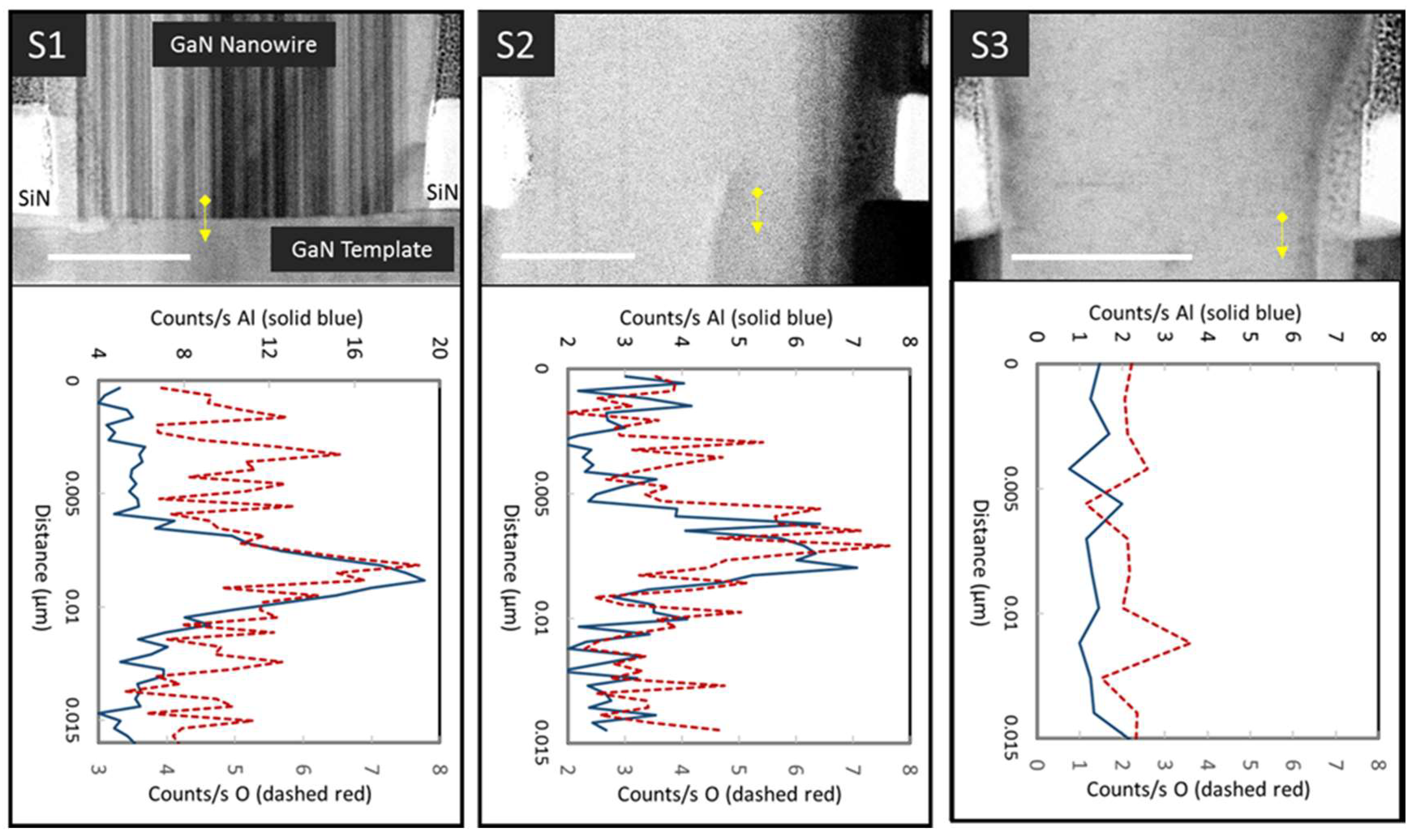
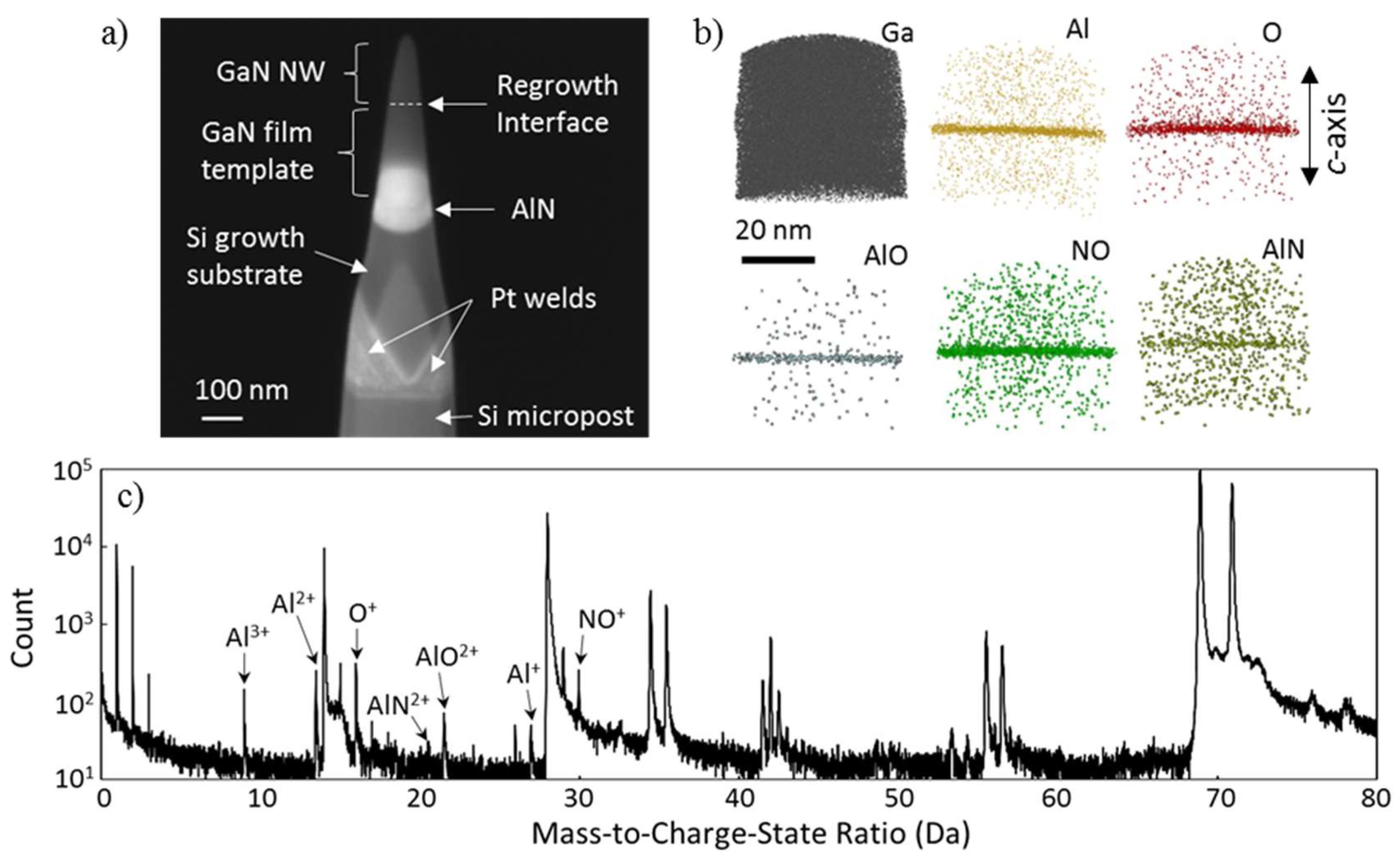
3.1. TEM Imaging
3.2. Atom Probe Tomography Characterization
4. Discussion
5. Conclusions
Author Contributions
Conflicts of Interest
References
- Brubaker, M.D.; Duff, S.M.; Harvey, T.E.; Blanchard, P.T.; Roshko, A.; Sanders, A.W.; Sanford, N.A.; Bertness, K.A. Polarity-Controlled GaN/AlN Nucleation Layers for Selective-Area Growth of GaN Nanowire Arrays on Si(111) Substrates by Molecular Beam Epitaxy. Cryst. Growth Des. 2016, 16, 596–604. [Google Scholar] [CrossRef]
- Albert, S.; Bengoechea-Encabo, A.; Sanchez-Garcia, M.A.; Kong, X.; Trampert, A.; Calleja, E. Selective area growth of In(Ga)N/GaN nanocolumns by molecular beam epitaxy on GaN-buffered Si(111): From ultraviolet to infrared emission. Nanotechnology 2013, 24, 175303. [Google Scholar] [CrossRef] [PubMed]
- Bengoechea-Encabo, A.; Albert, S.; Sanchez-Garcia, M.A.; Lopez, L.L.; Estrade, S.; Rebled, J.M.; Peiro, F.; Nataf, G.; de Merry, P.; Zuniga-Perez, J.; et al. Selective area growth of a- and c-plane GaN nanocolumns by molecular beam epitaxy using colloidal nanolithography. J. Cryst. Growth 2012, 353, 1–4. [Google Scholar] [CrossRef] [Green Version]
- Bertness, K.A.; Sanders, A.W.; Rourke, D.M.; Harvey, T.E.; Roshko, A.; Schlager, J.B.; Sanford, N.A. Controlled Nucleation of GaN Nanowires Grown with Molecular Beam Epitaxy. Adv. Funct. Mater. 2010, 20, 2911–2915. [Google Scholar] [CrossRef]
- Kishino, K.; Sekiguchia, H.; Kikuchi, A. Improved Ti-mask selective-area growth (SAG) by rf-plasma-assisted molecular beam epitaxy demonstrating extremely uniform GaN nanocolumn arrays. J. Cryst. Growth 2009, 311, 2063–2068. [Google Scholar] [CrossRef]
- Wu, C.H.; Lee, P.Y.; Chen, K.Y.; Tseng, Y.T.; Wang, Y.L.; Cheng, K.Y. Selective area growth of high-density GaN nanowire arrays on Si(111) using thin AlN seeding layers. J. Cryst. Growth 2016, 454, 71–81. [Google Scholar] [CrossRef]
- Kishino, K.; Yanagihara, A.; Ikeda, K.; Yamano, K. Monolithic integration of four-colour InGaN-based nanocolumn LEDs. Electron. Lett. 2015, 51, 852–854. [Google Scholar] [CrossRef]
- Kum, H.; Seong, H.K.; Lim, W.; Chun, D.; Kim, Y.I.; Park, Y.; Yoo, G. Wafer-scale Thermodynamically Stable GaN Nanorods via TwoStep Self-Limiting Epitaxy for Optoelectronic Applications. Sci. Rep. 2017, 7, 40893. [Google Scholar] [CrossRef] [PubMed]
- Zhao, S.R.; Nguyen, H.P.T.; Kibria, M.G.; Mi, Z.T. III-Nitride nanowire optoelectronics. Prog. Quantum Electron. 2015, 44, 14–68. [Google Scholar] [CrossRef]
- Hauswald, C.; Giuntoni, I.; Flissikowski, T.; Gotschke, T.; Calarco, R.; Grahn, H.T.; Geelhaar, L.; Brandt, O. Luminous Efficiency of Ordered Arrays of GaN Nanowires with Subwavelength Diameters. ACS Photonics 2017, 4, 52–62. [Google Scholar] [CrossRef]
- Kong, X.; Li, H.; Albert, S.; Bengoechea-Encabo, A.; Sanchez-Garcia, M.A.; Calleja, E.; Draxl, C.; Trampert, A. Titanium induced polarity inversion in ordered (In,Ga)N/GaN nanocolumns. Nanotechnology 2016, 27, 7. [Google Scholar] [CrossRef] [PubMed]
- Giannuzzi, L.A.; Drown, J.L.; Brown, S.R.; Irwin, R.B.; Stevie, F. Applications of the FIB lift-out technique for TEM specimen preparation. Microsc. Res. Tech. 1998, 41, 285–290. [Google Scholar] [CrossRef]
- Thompson, K.; Lawrence, D.; Larson, D.J.; Olson, J.D.; Kelly, T.F.; Gorman, B. In situ site-specific specimen preparation for atom probe tomography. Ultramicroscopy 2007, 107, 131–139. [Google Scholar] [CrossRef] [PubMed]
- Sanford, N.A.; Blanchard, P.T.; Davydov, A.V. Laser-Assisted Atom Probe Tomography of AlN and AlGaN. In Proceedings of the 59th Electronic Materials Conference, University of Notre Dame, South Bend, IN, USA, 28–30 June 2017. [Google Scholar]
- Roshko, A.; Brubaker, M.D.; Blanchard, P.T.; Bertness, K.A.; Harvey, T.E.; Geiss, R.H.; Levin, I. Comparison of convergent beam electron diffraction and annular bright field atomic imaging for GaN polarity determination. J. Mater. Res. 2017, 32, 936–946. [Google Scholar] [CrossRef]
- Diercks, D.R.; Gorman, B.P.; Kirchhofer, R.; Sanford, N.; Bertness, K.; Brubaker, M. Atom probe tomography evaporation behavior of C-axis GaN nanowires: Crystallographic, stoichiometric, and detection efficiency aspects. J. Appl. Phys. 2013, 114, 184903-1-9. [Google Scholar] [CrossRef]
- Meisenkothen, F.; Steel, E.B.; Prosa, T.J.; Henry, K.T.; Kolli, R.P. Effects of detector dead-time on quantitative analyses involving boron and multi-hit detection events in atom probe tomography. Ultramicroscopy 2015, 159, 101–111. [Google Scholar] [CrossRef] [PubMed]
- Matsubara, T.; Denpo, Y.; Okada, N.; Tadatomo, K. V-shaped pits in HVPE-grown GaN associated with columnar inversion domains originating from foreign particles of α-Si3N4 and graphitic carbon. Micron 2017, 94, 9–14. [Google Scholar] [CrossRef] [PubMed]
- Sanchez, A.T.; Dimitrakopoulos, G.P.; Ruterana, P. Mechanisms for the formation of inversion domains in GaN. In Microscopy of Semiconducting Materials 2003; Cullis, A.G., Midgley, P.A., Eds.; CRC Press: Boca Raton, FL, USA, 2003; pp. 269–272. [Google Scholar]
- Zhou, H.; Phillipp, F.; Schroder, H.; Bell, J.M. Influence of domain boundaries on polarity of GaN grown on sapphire. Appl. Surf. Sci. 2005, 252, 483–487. [Google Scholar] [CrossRef]
- Hite, J.K.; Garces, N.Y.; Goswami, R.; Mastro, M.A.; Kub, F.J.; Eddy, C.R. Selective switching of GaN polarity on Ga-polar GaN using atomic layer deposited Al2O3. Appl. Phys. Express 2014, 7, 025502-1-4. [Google Scholar] [CrossRef]

| Sample Description | Acid Treatment | Approximate # of Visible Inversion Domains per NW Cross Section | TEM EDS Counts per Second | Estimated fML by L-APT | ||
|---|---|---|---|---|---|---|
| Al | O | Al | O | |||
| S1: NW/GaN buffer interface | HF vapor | 25+ | 11 | 6 | 0.11 | 0.12 |
| S2: NW/GaN buffer interface | HF vapor | 2 to 4 | 3 | 3 | 0.05 | 0.09 |
| S3: NW/GaN buffer interface | HCl dip | 0 to 1 | 0 | 0 | 0 | 0.05 |
| S1-m: SiN mask/GaN buffer interface | -- | -- | 0 | 5 | 0 | 0.14 |
© 2018 by the authors. Licensee MDPI, Basel, Switzerland. This article is an open access article distributed under the terms and conditions of the Creative Commons Attribution (CC BY) license (http://creativecommons.org/licenses/by/4.0/).
Share and Cite
Blanchard, P.; Brubaker, M.; Harvey, T.; Roshko, A.; Sanford, N.; Weber, J.; Bertness, K.A. Characterization of Sub-Monolayer Contaminants at the Regrowth Interface in GaN Nanowires Grown by Selective-Area Molecular Beam Epitaxy. Crystals 2018, 8, 178. https://doi.org/10.3390/cryst8040178
Blanchard P, Brubaker M, Harvey T, Roshko A, Sanford N, Weber J, Bertness KA. Characterization of Sub-Monolayer Contaminants at the Regrowth Interface in GaN Nanowires Grown by Selective-Area Molecular Beam Epitaxy. Crystals. 2018; 8(4):178. https://doi.org/10.3390/cryst8040178
Chicago/Turabian StyleBlanchard, Paul, Matt Brubaker, Todd Harvey, Alexana Roshko, Norman Sanford, Joel Weber, and Kris A. Bertness. 2018. "Characterization of Sub-Monolayer Contaminants at the Regrowth Interface in GaN Nanowires Grown by Selective-Area Molecular Beam Epitaxy" Crystals 8, no. 4: 178. https://doi.org/10.3390/cryst8040178