Twin Domains in Organometallic Halide Perovskite Thin-Films
by
 and
and
Wei Liu
1, 
Yang Liu
1,
Ju Wang
1,
Cuncun Wu
1,
Congyue Liu
1,
Lixin Xiao
1,
Zhijian Chen
1,
Shufeng Wang
1,2,* and
Qihuang Gong
1,2 1
State Key Laboratory for Artificial Microstructure and Mesoscopic Physics, Department of Physics, Peking University, Beijing 100871, China
2
Collaborative Innovation Center of Extreme Optics, Shanxi University, Taiyuan 030006, China
*
Author to whom correspondence should be addressed.
Crystals 2018, 8(5), 216; https://doi.org/10.3390/cryst8050216
Submission received: 30 March 2018
/
Revised: 25 April 2018
/
Accepted: 11 May 2018
/
Published: 16 May 2018
(This article belongs to the Special Issue Metal Halide Perovskite Crystals: Growth Techniques, Properties and Emerging Applications)
Abstract
:The perovskite is a class of material with crystalline structure similar to CaTiO3. In recent years, the organic-inorganic hybrid metallic halide perovskite has been widely investigated as a promising material for a new generation photovoltaic device, whose power conversion efficiency (PCE) record reaches 22.7%. One of its underlying morphological characteristics is the twin domain within those sub-micron sized crystal grains in perovskite thin films. This is important for discussion since it could be the key for understanding the fundamental mechanism of the device’s high performance, such as long diffusion distance and low recombination rate. This review aims to summarize studies on twin domains in perovskite thin films, in order to figure out its importance, guide the current studies on mechanism, and design new devices. Firstly, we introduce the research history and characteristics of widely known twin domains in inorganic perovskite BaTiO3. We then focus on the impact of the domain structure emerging in hybrid metallic halide perovskite thin films, including the observation and discussion on ferroelectricity/ferroelasity. The theoretical analysis is also presented in this review. Finally, we present a spectroscopic method, which can reveal the generality of twin domains within perovskite thin films. We anticipate that this summary on the structural and physical properties of organometallic halide perovskite will help to understand and improve the high-performance of photovoltaic devices.

1. Introduction
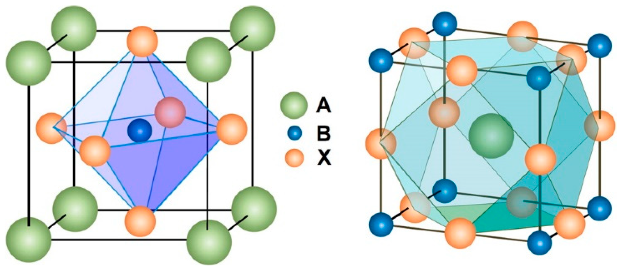
Perovskite, which is named after the Russian mineralogist Lev Perovski (1792–1856), is a widely known material whose discovery should be traced back to 1839 by Gustav Rose [1]. From the perspective of lattice structure, perovskite represents a group of material with ABX3 stoichiometry, whose crystalline structure is similar to CaTiO3 [2]. CH3NH3PbI3 (MAPbI3) is an organic–inorganic hybrid metallic halide perovskite with the unit cell containing Pb2+ and I−, forming a octahedral BX6 3D network, and together with cuboctahedral AX12 where MA+ occupies the center as seen in Figure 1 [3]. Since its first report with power conversion efficiency (PCE) 3.8% for a dye-sensitized solar cell in 2009 [4], its promising potentiality as the next generation photovoltaic material was soon discovered. A high PCE record of 22.7%, comparable to silicon-based solar cells, was achieved recently [5]. It has been widely applied to various forms of optoelectronic devices, such as lasers [6,7], light emitting diodes (LED) [8,9], photodetectors [10], and photovoltaic devices [11,12].
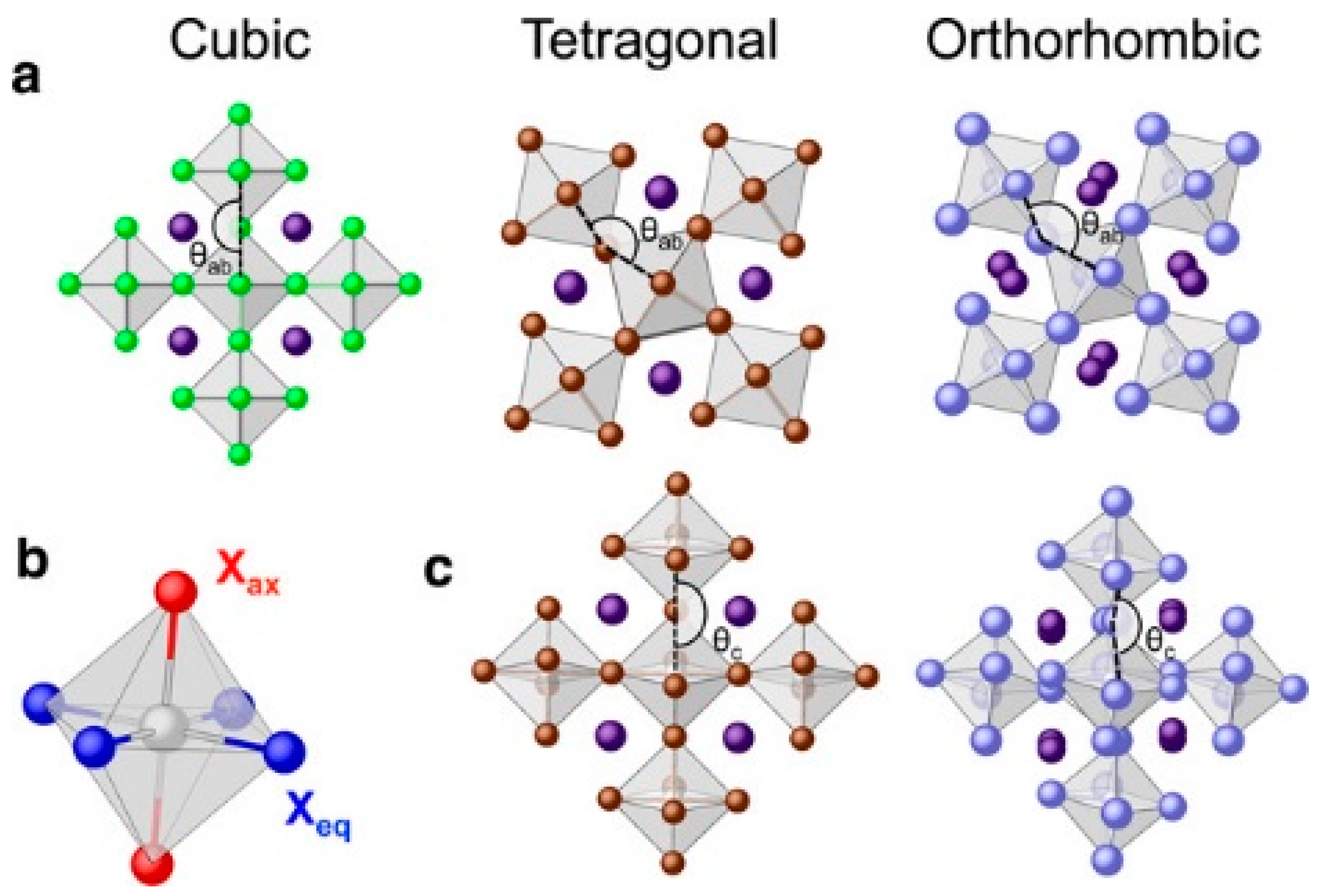
The phase transition of organometallic halide perovskite within the heating process has been widely studied in recent years. In MAPbI3, the octahedral (BX6) tilting with halide elements, which arises from the disordered orientation of methylammonium cation depending on the temperature and represents the bending of Pb-I-Pb bonding angle, provides possibility of three crystalline configurations with increased temperature as seen in Figure 2 [13,14]. Cubic phase is an ideal perovskite structure without tilts () which is maintained and stabilized above 327 K [13,15]. However, the tilts may present in the equatorial plane Xeq only ( and , rotation leading to a tetragonal phase between 162 K and 327 K) or together with tilting along the axial direction Xax ( and , rotation leading to an orthorhombic phase below 162 K) [13,15]. The phase transition of MAPbI3 from cubic crystalline structure to tetragonal together with lowered symmetry during the annealing process provides the possibility of intrinsic twin domains, similar to the ferroelectric ones within inorganic perovskite BaTiO3 films [16]. Although they are hard to observe in MAPbI3 thin films under SEM, the related possible ferroelectricity has been proposed to explain the I–V hysteresis experimentally [17,18] and theoretically [19], as well as the low recombination rate [20]. Recently, a TEM result revealed its presence, which provided the clue to disclose the unique optoelectronic performance of organometallic halide perovskite [21].
In this review, after briefly summarizing the twin domain in the typical inorganic perovskite BaTiO3, we introduce the current studies on MAPbI3 thin films. Though observations on twin domains are quite limited at the moment, they effectively proved the possibility of their existence, and the significance to discuss the charge carrier extraction based on the domain structure. E.g., the calculation based on first principle theory revealed that the structure could provide an additional channel for charge carrier transportation separately without recombination. At last, we introduce our newly developed optical method, which revealed the general existence of these subgrain microstructures in the organometallic perovskite thin films. At the moment, the connection between the twin domain and high performance is still missing and hard to fulfill. The direct observation on charge transportation along the structure is necessary to solve the connection. We summarize these studies in this review and expect the coming of this observation, in order to finally clarify the mechanism of these optoelectronic devices’ high performance. This mechanism would be different to any other high performance solar cells, such as silicon solar cells, thin film solar cells like CIGS, dye sensitized solar cells, and organic solar cells. We hope that the understanding of a new mechanism would help to improve the perovskite solar cells for high performance and the investigation of new photovoltaic materials.
2. Twin Domains in Inorganic Perovskite BaTiO3
Twin domain is an intrinsic morphological feature observed in non-central symmetric crystalline structures. Research on its origination and physical properties have a long history since the concept was first introduced with scientific description in 1783 [22]. However, the unambiguous definition of twinning is still missing in the literature owing to the structure complexity and various morphological phenomena [23]. One typical definition based on geometry of twinning crystal points out that “twin is a complex crystalline edifice built up of two or more homogeneous portions of the same crystal species in juxtaposition and oriented with respect to each other according to the well-defined twin laws” [23]. Twin domains could be classified into growth twinning, mechanical twinning, and transformation twinning under the consideration of formation mechanism, in spite of its various definitions [24].
Growth twinning can occur during the crystal growth, either at the nucleation stage [24] or by the oriented attachment [25]. For the former one, twinning is mainly the result of the growing mistake when some atoms or clusters of atoms arrive at the twin orientation and then continue to grow into a spread individual. A typical example is penetration twin domains observed in FeBO3 [26], quartz–homeotypic FePO4 [27], GaPO4 [28], Al2O3 [29], and some metallic materials like Zr and Ti [30]. Alternatively, in supersaturated solution condition, another type of growth twinning may occur on the base of twinned nucleation according to the theory of Buerger [24]. Under the later circumstance, growth twinning that resulted from the oriented attachment has not been widely studied yet. Some direct and indirect evidences including alum and β-quartz were reviewed by Massimo Nespolo and Giovanni Ferraris [25].
A mechanical pressure can switch the orientation of some crystals to another state while keeping the identical crystalline structure [24]. This result is regarded as mechanical twinning [31], which can be found in metals and minerals with elasticity and plasticity. They are shown as the rolling and shear texture in brass [32], stress-induced ω phase transition in β titanium alloys [33], and stacked microtwins of a few tens of nanometers in high manganese content austenitic steel [34] etc. It is worth mentioning that the ferroelastic transformation twin can be classified into mechanical twinning since it can be created by the shear deformation, resulting from mechanical load [35], such as the domain reorientation of ZrO2 under unidirectional compressive stress at high temperature [36], the prominent W domain walls observed in BiVO4 [37], a completely reversible domain structure induced by the high stress applied at the crack tip in BaTiO3 [38].
Twinning domains formed during crystalline phase transition in numerous optoelectronic materials are usually defined as transformation twinning. Generally, the transformation twinning is intimately related to the change of crystalline symmetry. Twin domains turn out during the cooling down process from high to low temperature, while the crystal phase transits from higher symmetry to lower symmetry, owing to the movements of cooperative atom in a nuclear region that is attributed to the loss of symmetry [39]. Well-known examples of the transformation twinning are revealed in perovskite, which obey the twin laws of high-low symmetry transition.
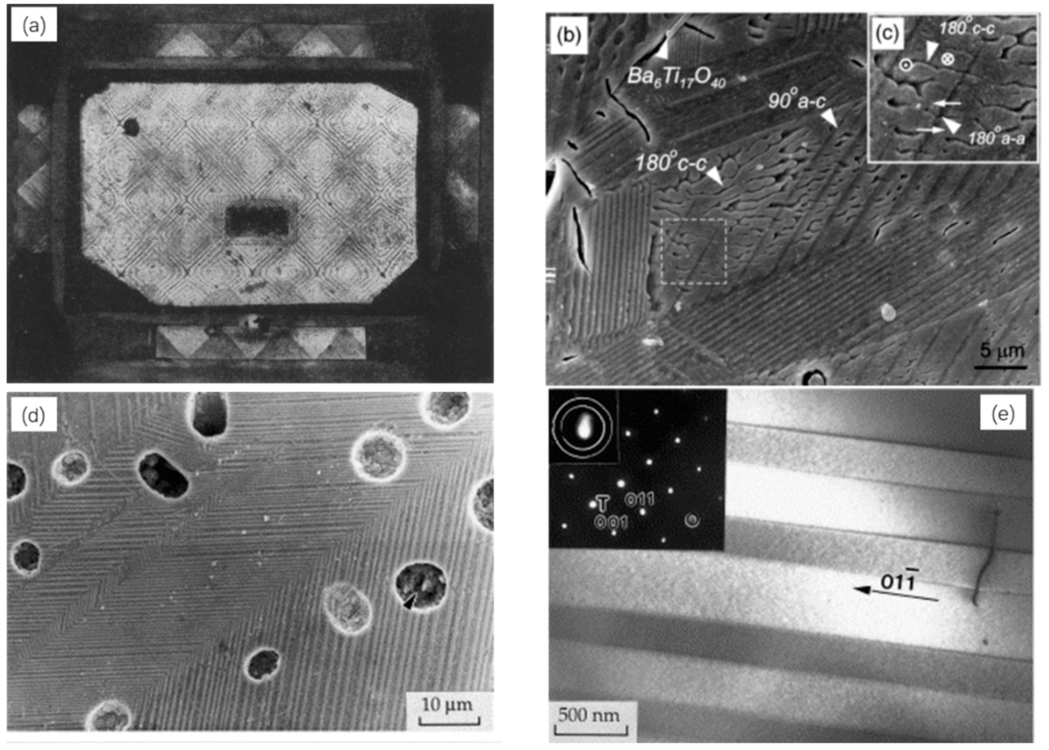
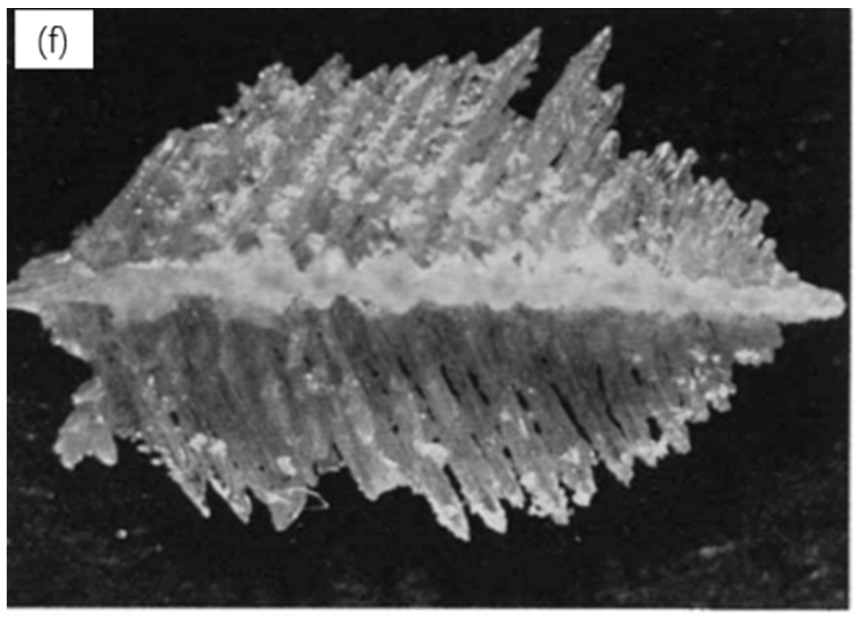
BaTiO3 is a typical representative of inorganic perovskite, which is commonly used today for numerous applications due to its ferroelectricity and piezoelectricity. BaTiO3 crystal is of cubic phase and centrosymmetric lattice structure above 120 °C [40]. The crystal would transform into a polar tetragonal phase with the emerging of the complex twin domains upon cooling. Basically, there are two kinds of twinnings according to the direction of the polar axis between adjacent twined domains: perpendicular (90° domain) or antiparallel (180° domain) [40]. One way to distinguish them is through polarized optical detection. Under the polarized light, responses are the same for the adjacent 180° domains. For 90° type, it could be justified by the observation of wedge-shaped lamella domains as seen the square-net pattern in Figure 3a, which were almost always identified under the polarized light in the tetragonal BaTiO3 single crystal [41,42]. Actually, the twin domain could be more unambiguous by etching or external electric field when photographed by optical microscopy, TEM, and SEM [43,44]. A typical BaTiO3 90° domain with characteristic banded domain structure of herringbone is showed in Figure 3d. The corresponding TEM bright field image of the same sample as seen in Figure 3e, which illustrated twin domains with width varied in 300~500 nm. The insetting selected area diffraction pattern (SADP), which showed the spot splitting subtending an angle of ~35° along the [110] direction, indicated that they were the 90° a–a type domains [45]. The twinning photograph confirmed that the BaTiO3 90° domain was prominent in the twin domains [42,46]. On the other hand, the Figure 3b,c illustrated the classical BaTiO3 180° twin domains, which were presented with image contrast resembling watermark patterns characterized by irregular lines, were embedded in the lamellar-shaped 90° domains. One more thing to be mentioned is that the growth twinning of BaTiO3 may emerge due to the mistake of nucleation during the crystal growing process. Figure 3f shows the famous growth twinning butterfly of BaTiO3 which relates to the cooling rate and the presence of certain impurities [47,48].
3. Subgrain Twin Domains Observed in MAPbI3
Photovoltaic devices based on methylammonium lead iodide perovskite have astonished breakthroughs in solar energy conversion efficiency in these years. Light absorber layers of perovskite solar cells are usually polycrystalline thin films, in which subgrain microstructures are rarely observed. Therefore, early research on the impact of microstructure in perovskite films was mainly focused only on the grain, including grain size and grain boundary. Choi et al. and Grancini et al. reported that the absorption spectrum of MAPbI3 in the mesoporous TiO2 with smaller grain size (few tens of nanometers) performed a blue shift compared to perovskite thin films deposited the flat substrate with larger grain size (hundreds of nanometers) [49,50]. Bastiani et al. and D’Innocenzo et al. claimed that the smaller grain size of the perovskite material, the shorter lifetime of the photoluminescence from the perspective of charge carrier dynamics [51,52], which was contrary to the result of Nie et al. [53]. The evidence showed that the fluorescence quenching in single crystal perovskite was even stronger [54,55]. The effect of perovskite grain boundary on the optoelectronic prosperities also received a large amount of attention. Dane W. de Quilette et al. reported that the fluorescence intensity of the MAPbI3−xClx grain boundary decreased to 65% compared to the inter grain by using confocal fluorescence microscopy [56]. The result meant that the grain boundary of perovskite material provided much excess non-radiation recombination pathway [56]. Interestingly, Yun et al. utilized KPFM and AFM to explore the impact of perovskite grain boundary with sunlight illumination. Their result showed that there were higher surface photovoltage and short circuit current in the grain boundary rather than the inter grain [57]. Their later work revealed that the grain boundary may benefit the charge separation and charge transportation [58].
There is no consensus about the impact of grain size and grain boundary on charge carrier dynamics and photovoltaic performance according to these contradictory studies. It results in challenge to the explanations about the remarkable photovoltaic efficiency, the mechanism of current-voltage hysteresis (I–V hysteresis) [17], and the impact of ion migration [59]. One fundamental question is about the origin of low recombination rate, which is contradicted to the Langvin recombination model [60]. The ambiguous understanding of these questions indicates the urgency of exploring the underlying mechanisms.
Recently, subgrain twin domains were found in MAPbI3 thin films [21,61,62,63,64]. These intra microstructures within grains may be the intrinsic potential factors in charging the high performance of perovskite-based photovoltaic devices [65]. Prior to the discovery of twin domain, the organolead perovskite had been proposed as ferroelectric [66,67,68]. However, whether the organometallic perovskite such as MAPbI3 possesses ferroelectricity remains ambiguous. We summarize some of the debates in Table 1.
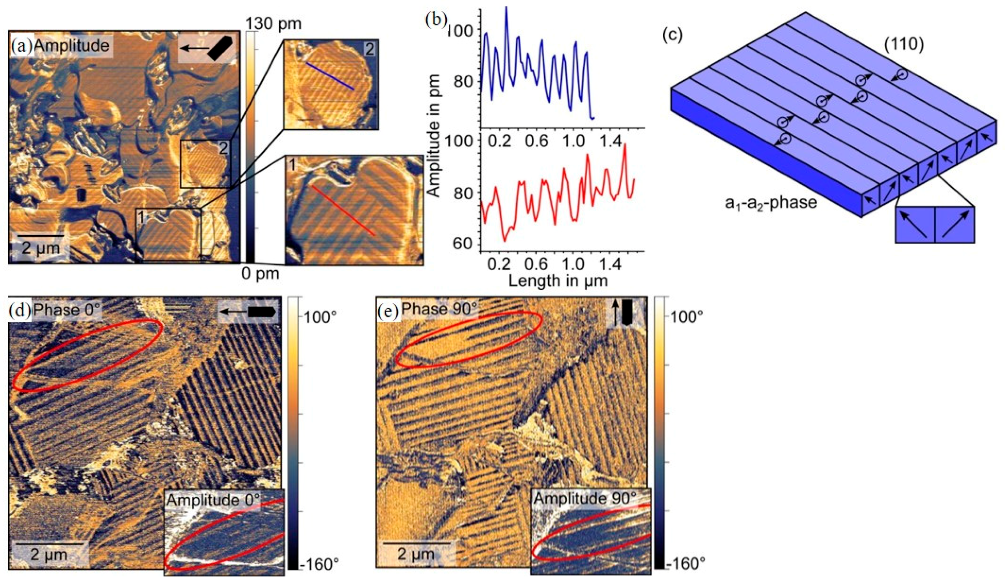
Whether the twinning structure represent ferroelectric or not keeps coming up as a question. Hermes et al. employed piezoresponse force microscopy (PFM) to characterize the a relative large and flat surfaces of MAPbI3 films [61]. Their results revealed the existence of subgrain twin domains in the tetragonal phase. The nanoscale periodic striped domain within single grain is shown in Figure 4a,b. These striped domains have their identical width within 100–300 nm in one grain, but vary between different grains. The 90° angle of stripes within grains shown in the magnified areas was a fingerprint-like structure for ferroelastic twin domains. It was supported by an additional PFM experiment on 90° rotated sample, for which the inverted phase contrast was found, with almost unchanged amplitude contrast (Figure 4d,e) [61]. Hermes et al. also proposed that the orientation of the polarization in the observed twin domains was a1–a2 phase, as seen in Figure 4c [61].
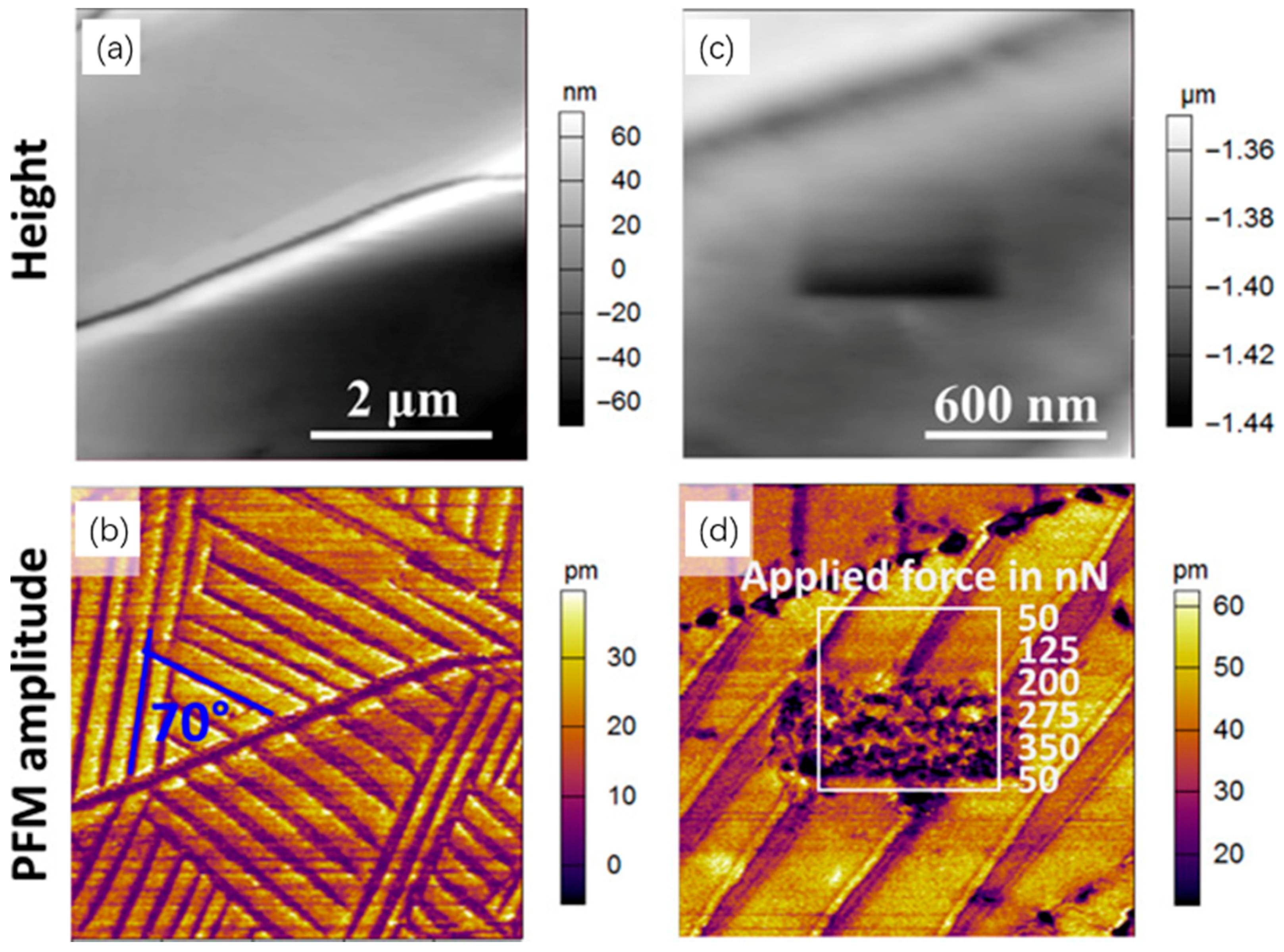
Furthermore, Strelcov et al. observed the 70° and 109° domain structure in MAPbI3 thin films with PFM, as seen in Figure 5 [62]. It was proven that the nanoscale domain behaved as a function of the applied stress, which would not return to the pristine state when the stress was relieved. It was in good agreement with the ferroelasticity [62]. In addition, the unchanged domain pattern under different electric field strength, observed by PTIR (Photothermal Induced Resonance), excluded the possibility of the ferroelectricity. Instead, it supported the ferroelastic nature of the structure [62].
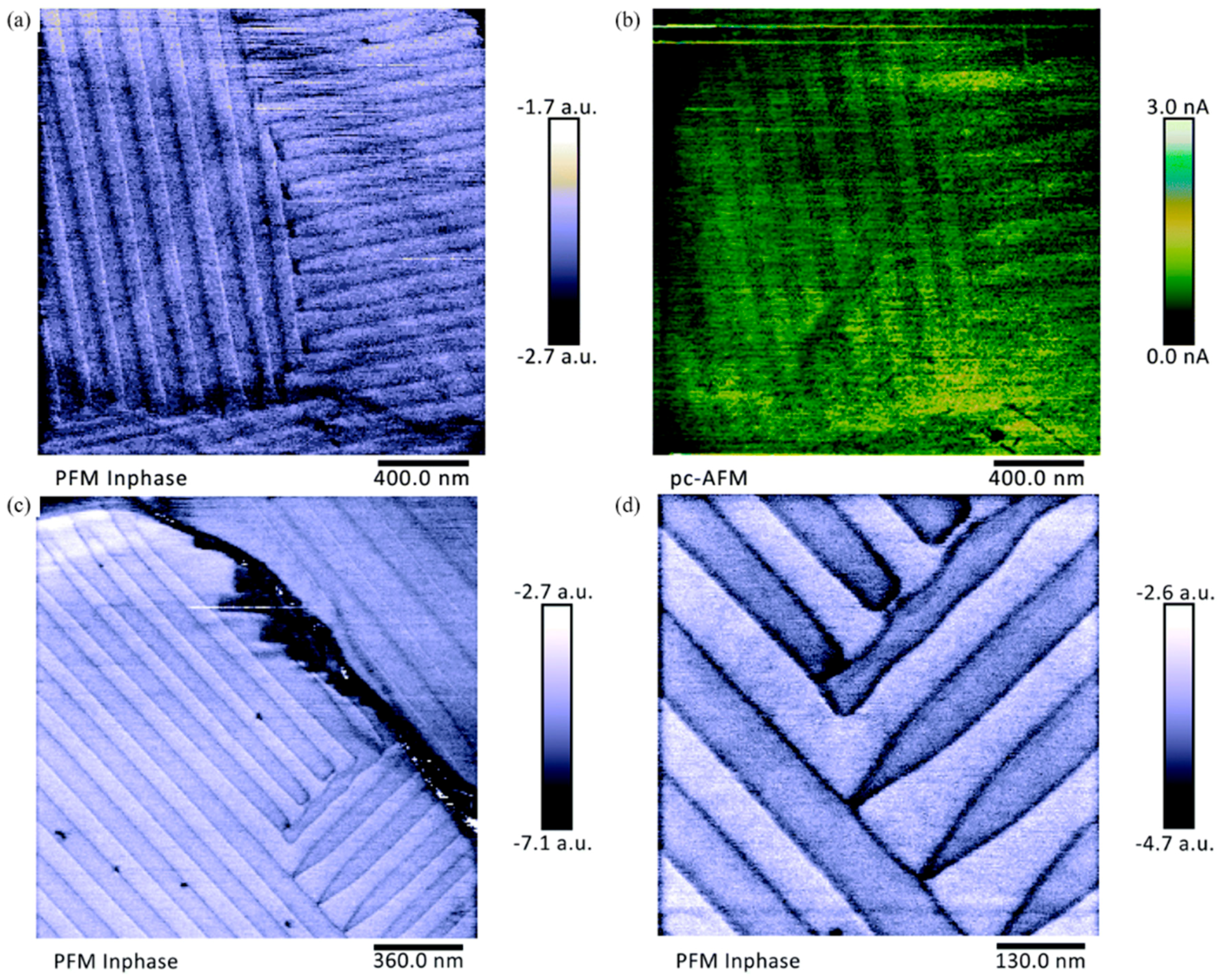
Recently, the alternating polarization striped domain with an average width of 90 nm was reported in solution-processed MAPbI3 film, as seen in Figure 6 [63]. Contrary to the previous report, these twin domains observed by PFM were considered as ferroelectric domains [63]. The 90° continuation of the domain within grains was observed clearly in Figure 6c,d, similar to the domains revealed by Hermes et al. [61]. Further investigation showed that the structure could provide 25% enhancement of the charge carriers extraction ability measured by the photo-conductive AFM (PC-AFM), as showed in Figure 6b [63].
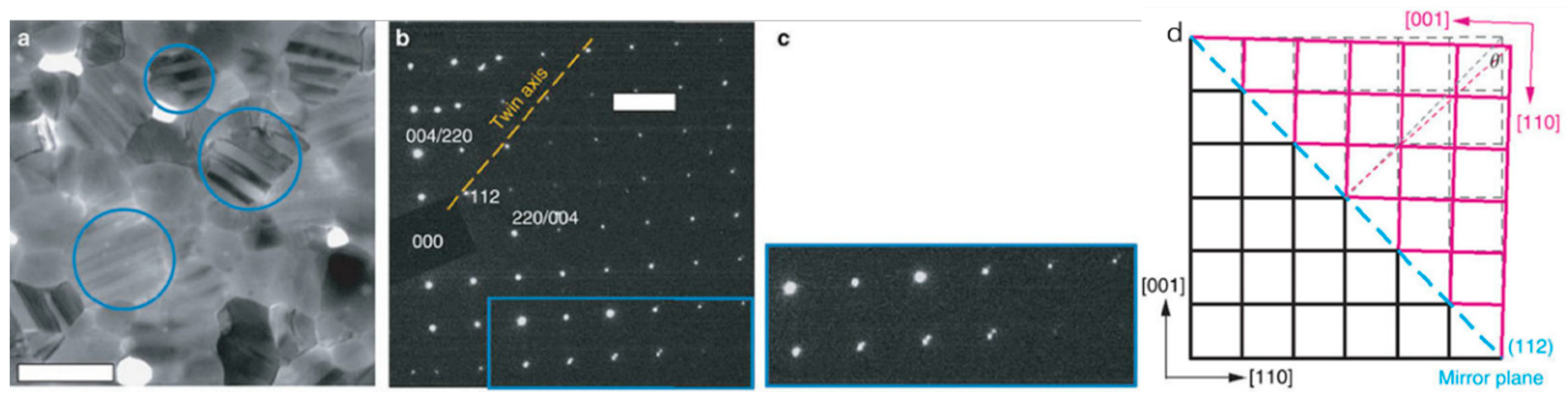
Employing PFM to detect subgrain twin domains is available for surface detection. However, the flat grain surface is needed to exclude the cross-talk of the surface structure with twinning morphology [63]. Hence, TEM, as a classical method to image twin domains in inorganic perovskite, is applied for investigating organometallic perovskite. Rothmann et al. reported intrinsic twin domains performed as ~100–300-nm-wide stripe in tetragonal phase MAPbI3 thin films as seen in Figure 7 [21]. These twin domains were observed with TEM under the condition of low electron dose and rapid acquisition to carefully avoid surface damage [21]. The selected area electron diffraction (SAED) result implied that the diffraction spot from adjacent domains were mirrored to each other across the twin axis and the twin axis was parallel [112] in direction. They claimed that the separation angle θ, which would be attributed to the difference of the lattice space distance of {110}t and {002}t planes at the tetragonal phase in MAPbI3, underpinned the twinning and formation of the {112}t twin plane [21]. They also found that the twin domain owed memorized characteristics. The striped contrast which existed at room temperature (tetragonal phase) disappeared in 70 °C (cubic phase). It turned out again when the sample cooled down to room temperature. This phase transformation-related phenomenon is consistent with the twin domain observed in inorganic perovskite BaTiO3 [16].
Another interesting study showed that the tetragonal and cubic phase coexisted at room temperature, observed by HRTEM in MAPbI3 thin films, as seen in Figure 8 [64]. The refinement of the HRTEM image, which was based on the Fourier filtering and reconstruction technique, showed that there were two types of spontaneously formed superlattices without composition change: triple layer superlattices made up of tetragonal/cubic/tetragonal stacking sequences and double layer superlattices made up of tetragonal/cubic stacking sequences. These spontaneous-formed superlattices were attributed to the structural transition under mixed tetragonal and cubic phase [64]. In addition, the atomically organized double layer superlattice was observed in the MAPbI3–TiO2 hetero-interface acting as a buffer layer, which provided possibility to benefit the photovoltaic performance due to enhanced charge transportation [64].
Rare observations about twin domains in MAPbI3 had been presented, although MAPbI3 films have been widely adopted as active layers in solar cells. The morphological characteristics of the twin domain in MAPbI3 films is hard to be summarized and some related growth conditions have benn summarized briefly in Table 2. Fortunately, there are abundant studies on inorganic perovskites. The studies showed that the morphology could be accounted to some factors such as grain size (g) and film thickness (t).
- According to the classical understanding, twin domains in ferroelastic or ferroelectric materials originate from the minimum energy evolution of the grain, with the expense of domain wall energy [16]. Therefore, the occurrence of twin domain related to the grain size g. A semi-quantitative model based on typical BaTiO3 twin domains revealed that the total elastic energy due to homogenous strain of phase transformation increased with g3 while the domain wall energy increased with g2. Research on BaTiO3 ceramics concluded that the domain width obeyed the g1/2 rule while g > 1 μm and the domain structure would no longer be unique with g < 1 μm [16]. Small twin structure of ~30 nm are observed in small grains of 300 nm [16].
- In ferroic material rhombohedral perovskite LSMO, it was revealed that the domain period followed the t1/2 rule in ultrathin films which implied high density of twin patterns at small film thickness and was, in turn, more apparent [74].
The normal grain size in MAPbI3 films is of a few hundred nanometers and a small twinning structure can be expected. Rough film surface is another obstacle for observation. High flatness of MAPbI3 films is needed for observing twin domain patterns during the PFM characterization process as suggested by Holger Röhm et al. [63]. However, the requirement for a real working layer has no strict requirement for surface flatness. Therefore, the twinning structures in MAPbI3 films are still hard to be studied.
4. Effect of the Subgrain Microstructure on Perovskite Solar Cells
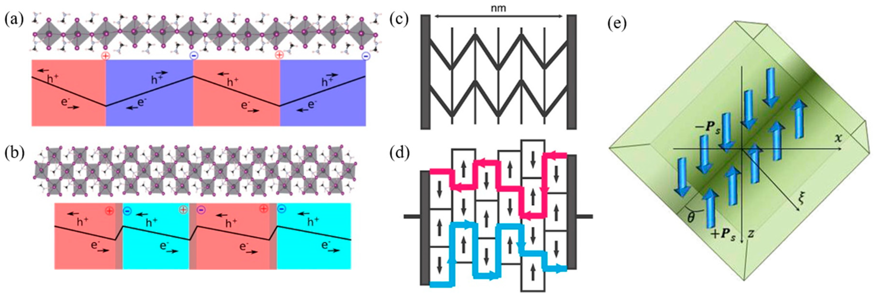
The subgrain twin domain in MAPbI3 could be related to ferroelasticity or ferroelectricity, which could explain the low recombination rate and long carrier diffusion distance. In inorganic perovskite ABX3 like BaTiO3, the B could move away from the center of the BX6 cage in the tetragonal phase leading to the broken crystal centro-symmetry and a spontaneous electric field in turn [75,76]. A similar mechanism was proposed by Frost et al., who suggested that the organic cation rotating in the inorganic cage relative to MAPbI3 could distort the lattice symmetry [20]. A corresponding electronic polarization field of 38 μC/cm2, comparable to the inorganic ferroelectric perovskite, was calculated [20]. Liu et al. presented the impact of ferroelectricity in the charge separation process based on the DFT calculation in MAPbI3 [77]. Their results illustrated that two possible mechanisms could benefit charge separation, for which the ferroelectric domain wall would be charged or uncharged due to the flexible rotation of MA+ in the crystal structure, as seen in Figure 9a,b. One was the electron-hole pair separation channel between the charged domain wall existing in 90° domain and 180° domain [77]. The other was the small polarization field normal to ferroelectric domain walls in the uncharged 90° domain wall [77]. Frost et al. explained the enhancement of charge carrier transport induced by the ferroelectric domain in detail with the ferroelectric highway configuration [20]. According to the proposed ferroelectric highway, the electron-hole pair could be separated efficiently within one ferroelectric domain due to the polarization field and the charge carrier diffused along the domain boundary freely toward the electrodes without recombination, as seen in Figure 9c,d [20]. Furthermore, the calculation based on Landau–Ginzburg–Devonshire theory revealed that the carrier diffused to ferroelectric domain wall and accumulated there, as seen in Figure 9e. The accumulation of charge carriers increased the static conductivity of the domain wall by 3–4 orders compared to the bulk state [78]. Recently, the density function theory based model revealed a similar segregation transport of electrons and holes with increased conductance and reduced bandgap in MAPbI3 [79].
Ambient experimental evidence to evaluate the positive or negative effect of subgrain microstructure observed in MAPbI3 thin films on perovskite solar cells is still missing although theoretical results stand by the positive side. However, some indirect evidence has been reported recently. Daniele Rossi et al. developed a drift-diffusion model to simulate the actual benefit of polarization field to the perovskite solar cells based on the revealed herring-bone like ferroelectric domains in their earlier work [63]. Their results illustrated that the ferroelectric domain suppressed the defect-mediated recombination and direct recombination owing to the discontinued polarization field which acted as an electron-hole separate pathway [80]. Hsinhan Tsai et al. investigated the structural dynamic evolution under continued light illumination, whose results illustrated the light-induced uniform lattice expansion leading to enhanced power conversion efficiency (from 18.5% to 20.5%) and stability (more than 1500 h) of perovskite solar cells [81]. Actually, the light-soaking process performed as annealing procedure, during which the lattice strain originated from phase transition was nonnegligible. Its rational to propose that the occurrence of twin domains resulted from lattice strain during the light illumination given by the formation mechanism of transformation twin domains. More indirect evidence of twin domains’ positive effect on photovoltaic devices has been suggested by the high performance and stability perovskite solar cells with nanoscale stripe patterns, especially the mixed-cation or mixed-halide perovskite such as (FAPbI3)0.85(MAPbI3)0.15 [82], MAPbI3−xClx [83], CsxFA1−xPbI3 [84].
5. Optical Method to Observe the Broad Existence of Subgrain Twin Domains
The subgrain twin domains, which are widely found in inorganic perovskite BaTiO3, remain mysterious in organometallic perovskite MAPbI3 working layers, though they have been observed with PFM and TEM in specified samples. As we mentioned in former parts, the surface roughness, the small scale of the domain, and the a1–a2 phase characteristics are the obstacles for direct observation in working layers [21,63]. Fortunately, we developed a convenient optical method to identify the broad existence of subgrain twin domains hidden in MAPbI3 active layers [85].
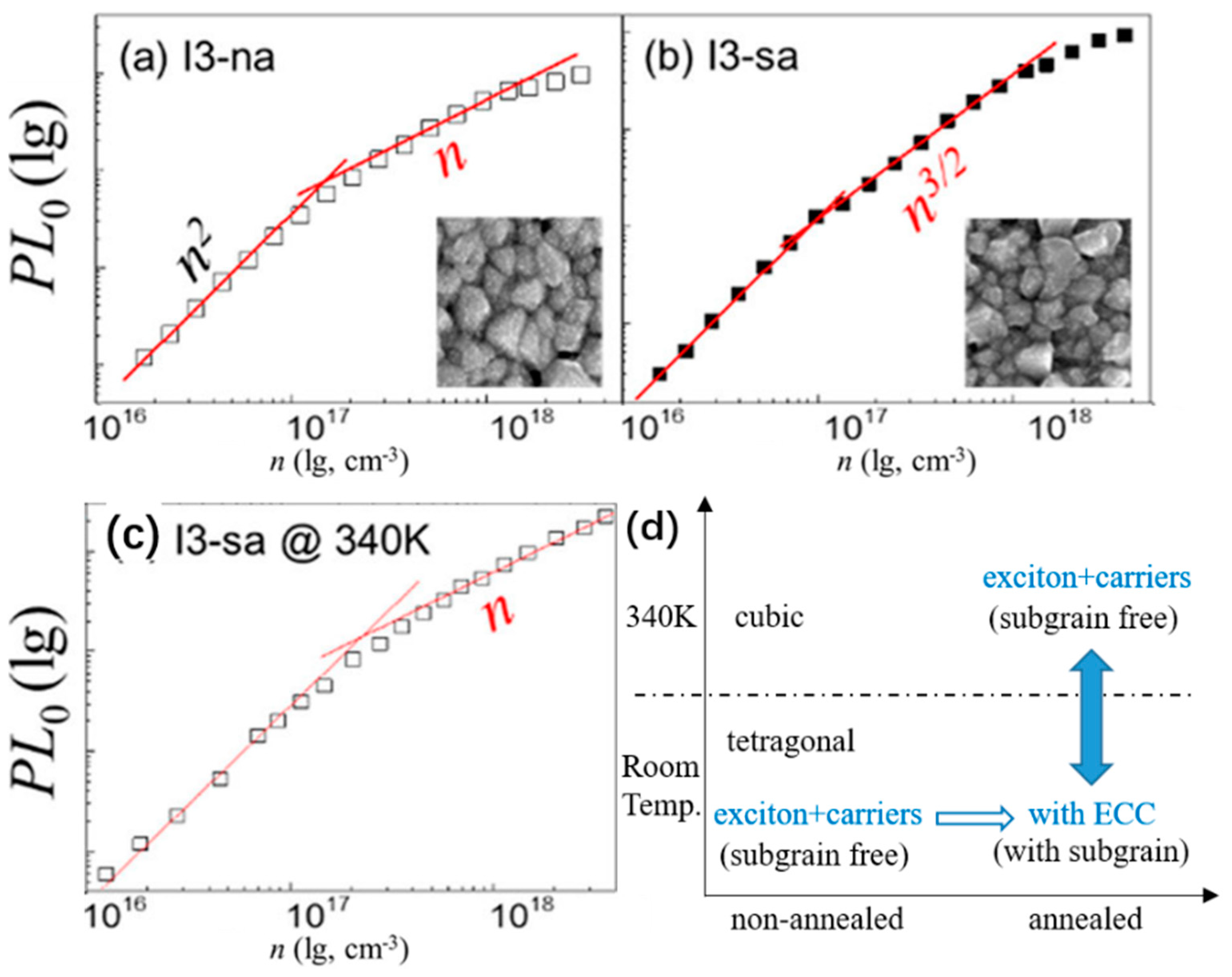
It is revealed that the photo-generated products, such as carriers, excitons, trions, and bi-exciton etc. strongly correlated to material morphology. This relationship requires some conditions. In principle, the morphology variation may not lead to change of photoproducts. E.g., larger and smaller crystal grains may have similar photophysical behaviors. However, on the other hand, if we reduce the grain size to the nano scale or lower its dimension to nanowire and two-dimensional layers, the photophysical behavior will be significantly different [86,87]. Therefore, if the variation on photoproducts is found, it would represent significant change in morphology. Based on this idea, the relationship between photoexcited exciton and free carriers was analyzed by our recently developed density-resolved spectroscopic method [88]. The method focuses on the excitation density-dependent photoproduct system, since the correlation of exciton and free carriers in semiconductors is density-dependent. According to the Saha–Langmuir equation [89] and fixed fluorescence intensity I(n) [88]:
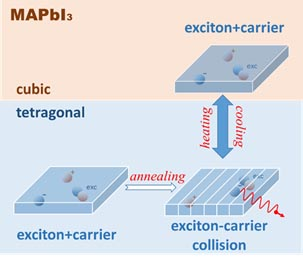
where is the total carrier intensity under light illumination, is the ratio of free carriers, , , , are the reduced effective mass, the Boltzmann constant, the Plank’s constant, the exciton binding energy. and represent the decay rate of monomolecular and bimolecular recombination, is another decay rate that originated from exciton–carrier collision (ECC). At high excitation density, the fixed fluorescence intensity I(n) performs as power index 1 representing coexistence of exciton and free carriers without ECC, while power index 3/2 which implies the dominance of ECC behavior at perovskite thin films [85].
For freshly made perovskite films without heat annealing (or slightly heated for removing solvent), the exciton and free carriers co-existed and interconverted to each other dynamically as shown in Figure 10a with obvious power index 1 at high excitation density. For thin films experiencing adequate heat annealing, the collision-induced quenching of exciton and free carriers (ECC) happened as illustrated in Figure 10b with power index 3/2 at high excitation density [85]. Since the non-annealed and annealed film were all with tetragonal phase, there must be some intrinsic morphological change appearing. In addition, when the fully annealed films (3/2 index) were heated to 340 K (above the phase transition temperature from tetragonal to cubic phase), the ECC disappeared (the index become 1), as seen in Figure 10c. However, the 3/2 index came back when the films were cooled down to room temperature. This initial annealing and phase transition dependent behavior was akin to the twin domain formation in BaTiO3 film and MAPbI3 films revealed by TEM [16,21]. Therefore, we confirmed that the subgrain morphology generated in MAPbI3 films and such subgrain morphology should be twin domains proposed in previous studies [85]. The photoproduct behavior and corresponding proposed mechanism are summarized in Figure 10d [85]. Our full analysis of the photoproduct system revealed the existence of twin domains in sufficiently annealed MAPbI3 thin films. By knowing the generality of the annealing process in perovskite thin film preparation process, it could be deduced that the broad existence of twin domains in perovskite solar cells which is in agreement with the previous surface morphology characterization [82,83,84], we are continuing further research to directly observe the charge transportation under the twin domain morphology.
6. Conclusions and Outlook
In this review, we give a detailed description of twin domains observed in inorganic and organometallic perovskite. We summarize the origin of twin domains emerged in metals and ceramics, together with explicit characterization of twin domain structure in typical inorganic perovskite BaTiO3. Some typical corresponding subgrain twin domains emerged in MAPbI3 thin films were revealed by PFM and TEM, given that the organometallic perovskite MAPbI3 possesses the lattice structure analogous to BaTiO3. Theoretical calculations about domain structure in MAPbI3 indicating its benefit to charge transport is summarized. A new spectroscopic method which could reveal the generality of subgrain twin domain in perovskite films is also introduced.
Despite the relatively ambiguous understanding on the subgrain twin domain of organometallic perovskite, the experimental characterization and theoretical calculation presented above illustrate its importance in effective charge transportation and high photovoltaic performance. To further understand and improve perovskite solar cells’ photovoltaic performance, tremendous attention on the origin and impact of the subgrain twin domain should be paid. One thing to be mentioned is that the subgrain twin domain of organometallic perovskite seems to correlate with the phase transformation from cubic phase to tetragonal phase akin to transformation twin of BaTiO3. It is reasonable to infer the normal existence of the subgrain twin domain in organometallic films, providing that the indispensable annealing during the thin-film preparation process, which emphasizes the significance to explore the subgrain twin domain. To our understanding, the study on twinning domain in MAPbI3 will finally reveal the fundamental mechanism of the material and the devices’ high performance.
Acknowledgments
This work supported by the National Basic Research Program of China 2016YFB0401003; National Natural Science Foundation of China under grant Nos. 11527901, 61775004, 61575005, 11574009, U1605244, and 91750203.
Conflicts of Interest
The authors declare no conflicts of interest.
References
- Perovskite Mineral Data. Available online: http://webmineral.com/data/Perovskite.shtml#.Wqd1auhubIU (accessed on 13 March 2018).
- Bhalla, A.S.; Guo, R.; Roy, R. The perovskite structure—A review of its role in ceramic science and technology. Mater. Res. Innov. 2000, 4, 3–26. [Google Scholar] [CrossRef]
- Kim, H.-S.; Im, S.H.; Park, N.-G. Organolead Halide Perovskite: New Horizons in Solar Cell Research. J. Phys. Chem. C 2014, 118, 5615–5625. [Google Scholar] [CrossRef]
- Kojima, A.; Teshima, K.; Shirai, Y.; Miyasaka, T. Organometal Halide Perovskites as Visible-Light Sensitizers for Photovoltaic Cells. J. Am. Chem. Soc. 2009, 131, 6050–6051. [Google Scholar] [CrossRef] [PubMed]
- Efficiency-Chart. Available online: Https://www.nrel.gov/pv/assets/images/efficiency-chart.png (accessed on 10 March 2018).
- Liu, P.; He, X.; Ren, J.; Liao, Q.; Yao, J.; Fu, H. Organic–Inorganic Hybrid Perovskite Nanowire Laser Arrays. ACS Nano 2017, 11, 5766–5773. [Google Scholar] [CrossRef] [PubMed]
- Zhu, H.; Fu, Y.; Meng, F.; Wu, X.; Gong, Z.; Ding, Q.; Gustafsson, M.V.; Trinh, M.T.; Jin, S.; Zhu, X.-Y. Lead halide perovskite nanowire lasers with low lasing thresholds and high quality factors. Nat. Mater. 2015, 14, 636–642. [Google Scholar] [CrossRef] [PubMed]
- Qin, X.; Dong, H.; Hu, W. Green light-emitting diode from bromine based organic-inorganic halide perovskite. Sci. China Mater. 2015, 58, 186–191. [Google Scholar] [CrossRef]
- Wang, N.; Cheng, L.; Ge, R.; Zhang, S.; Miao, Y.; Zou, W.; Yi, C.; Sun, Y.; Cao, Y.; Yang, R.; et al. Perovskite light-emitting diodes based on solution-processed self-organized multiple quantum wells. Nat. Photonics 2016, 10, 699–704. [Google Scholar] [CrossRef]
- Dou, L.; Yang, Y.; You, J.; Hong, Z.; Chang, W.-H.; Li, G.; Yang, Y. Solution-processed hybrid perovskite photodetectors with high detectivity. Nat. Commun. 2014, 5, 5404. [Google Scholar] [CrossRef] [PubMed]
- Liu, M.; Johnston, M.B.; Snaith, H.J. Efficient planar heterojunction perovskite solar cells by vapour deposition. Nature 2013, 501, 395–398. [Google Scholar] [CrossRef] [PubMed]
- Green, M.A.; Ho-Baillie, A.; Snaith, H.J. The emergence of perovskite solar cells. Nat. Photonics 2014, 8, 506–514. [Google Scholar] [CrossRef]
- Bertolotti, F.; Protesescu, L.; Kovalenko, M.V.; Yakunin, S.; Cervellino, A.; Billinge, S.J.L.; Terban, M.W.; Pedersen, J.S.; Masciocchi, N.; Guagliardi, A. Coherent Nanotwins and Dynamic Disorder in Cesium Lead Halide Perovskite Nanocrystals. ACS Nano 2017, 11, 3819–3831. [Google Scholar] [CrossRef] [PubMed]
- Weller, M.T.; Weber, O.J.; Henry, P.F.; Pumpo, A.M.D.; Hansen, T.C. Complete structure and cation orientation in the perovskite photovoltaic methylammonium lead iodide between 100 and 352 K. Chem. Commun. 2015, 51, 4180–4183. [Google Scholar] [CrossRef] [PubMed]
- Poglitsch, A.; Weber, D. Dynamic Disorder in Methylammoniumtrihalogenoplumbates(II) Observed by Millimeter-wave Spectroscopy. J. Chem. Phys. 1987, 87, 6373–6378. [Google Scholar] [CrossRef]
- Arlt, G. Twinning in ferroelectric and ferroelastic ceramics: Stress relief. J. Mater. Sci. 1990, 25, 2655–2666. [Google Scholar] [CrossRef]
- Snaith, H.J.; Abate, A.; Ball, J.M.; Eperon, G.E.; Leijtens, T.; Noel, N.K.; Stranks, S.D.; Wang, J.T.-W.; Wojciechowski, K.; Zhang, W. Anomalous Hysteresis in Perovskite Solar Cells. J. Phys. Chem. Lett. 2014, 5, 1511–1515. [Google Scholar] [CrossRef] [PubMed]
- Chen, H.-W.; Sakai, N.; Ikegami, M.; Miyasaka, T. Emergence of Hysteresis and Transient Ferroelectric Response in Organo-Lead Halide Perovskite Solar Cells. J. Phys. Chem. Lett. 2015, 6, 164–169. [Google Scholar] [CrossRef] [PubMed]
- Frost, J.M.; Butler, K.T.; Walsh, A. Molecular ferroelectric contributions to anomalous hysteresis in hybrid perovskite solar cells. APL Mater. 2014, 2, 081506. [Google Scholar] [CrossRef] [Green Version]
- Frost, J.M.; Butler, K.T.; Brivio, F.; Hendon, C.H.; van Schilfgaarde, M.; Walsh, A. Atomistic Origins of High-Performance in Hybrid Halide Perovskite Solar Cells. Nano Lett. 2014, 14, 2584–2590. [Google Scholar] [CrossRef] [PubMed] [Green Version]
- Rothmann, M.U.; Li, W.; Zhu, Y.; Bach, U.; Spiccia, L.; Etheridge, J.; Cheng, Y.-B. Direct observation of intrinsic twin domains in tetragonal CH3NH3PbI3. Nat. Commun. 2017, 8. [Google Scholar] [CrossRef] [PubMed]
- Janovec, V.; Hahn, T.; Klapper, H. Twinning and domain structures. In International Tables for Crystallography Volume D: Physical Properties of Crystals; International Tables for Crystallography; Springer: Dordrecht, The Netherlands, 2006; pp. 377–392. ISBN 978-1-4020-0714-9. [Google Scholar]
- Hahn, T.; Klapper, H. Twinning of crystals. In International Tables for Crystallography Volume D: Physical Properties of Crystals; Springer: Dordrecht, The Netherlands, 2006; pp. 393–448. [Google Scholar]
- Buerger, M.J. The genesis of twin crystals. Am. Mineral. 1945, 30, 469–482. [Google Scholar]
- Nespolo, M.; Ferraris, G. The oriented attachment mechanism in the formation of twins-a survey. Eur. J. Mineral. 2004, 16, 401–406. [Google Scholar] [CrossRef]
- Kotrbová, M.; Kadečková, S.; Novák, J.; Brádler, J.; Smirnov, G.V.; Shvydko, Y.V. Growth and perfection of flux grown FeBO3 and 57FeBO3 crystals. J. Cryst. Growth 1985, 71, 607–614. [Google Scholar] [CrossRef]
- Ng, H.N.; Calvo, C. Refinement of the Crystal Structure of the Low-quartz Modification of Ferric Phosphate. Can. J. Chem. 1975, 53, 2064–2067. [Google Scholar] [CrossRef]
- Engel, G.; Klapper, H.; Krempl, P.; Mang, H. Growth twinning in quartz-homeotypic gallium orthophosphate crystals. J. Cryst. Growth 1989, 94, 597–606. [Google Scholar] [CrossRef]
- Fang, X.-S.; Ye, C.-H.; Zhang, L.-D.; Xie, T. Twinning-Mediated Growth of Al2O3 Nanobelts and Their Enhanced Dielectric Responses. Adv. Mater. 2005, 17, 1661–1665. [Google Scholar] [CrossRef]
- Song, S.G.; Gray, G.T. Structural interpretation of the nucleation and growth of deformation twins in Zr and Ti—II. Tem study of twin morphology and defect reactions during twinning. Acta Metall. Mater. 1995, 43, 2339–2350. [Google Scholar] [CrossRef]
- Clayton, J.D. Mechanical Twinning in Crystal Plasticity. In Nonlinear Mechanics of Crystals; Solid Mechanics and Its Applications; Springer: Dordrecht, The Netherlands, 2011; pp. 379–421. ISBN 978-94-007-0349-0. [Google Scholar]
- Van Houtte, P. Simulation of the rolling and shear texture of brass by the Taylor theory adapted for mechanical twinning. Acta Metall. 1978, 26, 591–604. [Google Scholar] [CrossRef]
- Hanada, S.; Izumi, O. Transmission electron microscopic observations of mechanical twinning in metastable beta titanium alloys. Metall. Trans. A 1986, 17, 1409–1420. [Google Scholar] [CrossRef]
- Allain, S.; Chateau, J.-P.; Dahmoun, D.; Bouaziz, O. Modeling of mechanical twinning in a high manganese content austenitic steel. Mater. Sci. Eng. A 2004, 387–389, 272–276. [Google Scholar] [CrossRef]
- Březina, B.; Fousek, J. Twinning in Crystals. In Crystal Growth in Science and Technology; NATO ASI Series; Springer: Boston, MA, USA, 1989; pp. 185–195. ISBN 978-1-4612-7861-0. [Google Scholar]
- Chan, C.-J.; Lange, F.F.; Rühle, M.; Jue, J.-F.; Virkar, A.V. Ferroelastic Domain Switching in Tetragonal Zirconia Single Crystals—Microstructural Aspects. J. Am. Ceram. Soc. 1991, 74, 807–813. [Google Scholar] [CrossRef]
- Lim, A.R.; Choh, S.H.; Jang, M.S. Prominent ferroelastic domain walls in BiVO4 crystal. J. Phys. Condens. Matter 1995, 7, 7309. [Google Scholar] [CrossRef]
- Meschke, F.; Kolleck, A.; Schneider, G.A. R-curve behaviour of BaTiO3 due to stress-induced ferroelastic domain switching. J. Eur. Ceram. Soc. 1997, 17, 1143–1149. [Google Scholar] [CrossRef]
- Cahn, R.W. Twinned crystals. Adv. Phys. 1954, 3, 363–445. [Google Scholar] [CrossRef]
- Cook, W.R. Domain Twinning in Barium Titanate Ceramics. J. Am. Ceram. Soc. 1956, 39, 17–19. [Google Scholar] [CrossRef]
- Forsbergh, P.W. Domain Structures and Phase Transitions in Barium Titanate. Phys. Rev. 1949, 76, 1187–1201. [Google Scholar] [CrossRef]
- Cheng, S.-Y.; Ho, N.-J.; Lu, H.-Y. Transformation-Induced Twinning: The 90° and 180° Ferroelectric Domains in Tetragonal Barium Titanate. J. Am. Ceram. Soc. 2006, 89, 2177–2187. [Google Scholar] [CrossRef]
- Hooton, J.A.; Merz, W.J. Etch Patterns and Ferroelectric Domains in BaTiO3 Single Crystals. Phys. Rev. 1955, 98, 409–413. [Google Scholar] [CrossRef]
- Merz, W.J. Domain Formation and Domain Wall Motions in Ferroelectric BaTiO3 Single Crystals. Phys. Rev. 1954, 95, 690–698. [Google Scholar] [CrossRef]
- Chou, J.-F.; Lin, M.-H.; Lu, H.-Y. Ferroelectric domains in pressureless-sintered barium titanate. Acta Mater. 2000, 48, 3569–3579. [Google Scholar] [CrossRef]
- Klassen-Neklyudova, M.V. Mechanical Twinning of Crystals; Springer: Boston, MA, USA, 1964; ISBN 978-1-4684-1541-4. [Google Scholar]
- Nielsen, J.W.; Linares, R.C.; Koonce, S.E. Genesis of the Barium Titanate Butterfly Twin. J. Am. Ceram. Soc. 1962, 45, 12–17. [Google Scholar] [CrossRef]
- De Vries, R.C. Observations on Growth of BaTiO3, Crystals from KF Solutions. J. Am. Ceram. Soc. 1959, 42, 547–558. [Google Scholar] [CrossRef]
- Choi, J.J.; Yang, X.; Norman, Z.M.; Billinge, S.J.L.; Owen, J.S. Structure of Methylammonium Lead Iodide Within Mesoporous Titanium Dioxide: Active Material in High-Performance Perovskite Solar Cells. Nano Lett. 2014, 14, 127–133. [Google Scholar] [CrossRef] [PubMed]
- Grancini, G.; Marras, S.; Prato, M.; Giannini, C.; Quarti, C.; De Angelis, F.; De Bastiani, M.; Eperon, G.E.; Snaith, H.J.; Manna, L.; et al. The Impact of the Crystallization Processes on the Structural and Optical Properties of Hybrid Perovskite Films for Photovoltaics. J. Phys. Chem. Lett. 2014, 5, 3836–3842. [Google Scholar] [CrossRef] [PubMed]
- De Bastiani, M.; D’Innocenzo, V.; Stranks, S.D.; Snaith, H.J.; Petrozza, A. Role of the crystallization substrate on the photoluminescence properties of organo-lead mixed halides perovskites. APL Mater. 2014, 2, 081509. [Google Scholar] [CrossRef]
- D’Innocenzo, V.; Srimath Kandada, A.R.; De Bastiani, M.; Gandini, M.; Petrozza, A. Tuning the Light Emission Properties by Band Gap Engineering in Hybrid Lead Halide Perovskite. J. Am. Chem. Soc. 2014, 136, 17730–17733. [Google Scholar] [CrossRef] [PubMed]
- Nie, W.; Tsai, H.; Asadpour, R.; Blancon, J.-C.; Neukirch, A.J.; Gupta, G.; Crochet, J.J.; Chhowalla, M.; Tretiak, S.; Alam, M.A.; et al. High-efficiency solution-processed perovskite solar cells with millimeter-scale grains. Science 2015, 347, 522–525. [Google Scholar] [CrossRef] [PubMed]
- Yamada, Y.; Yamada, T.; Phuong, L.Q.; Maruyama, N.; Nishimura, H.; Wakamiya, A.; Murata, Y.; Kanemitsu, Y. Dynamic Optical Properties of CH3NH3PbI3 Single Crystals as Revealed by One- and Two-Photon Excited Photoluminescence Measurements. J. Am. Chem. Soc. 2015, 137, 10456–10459. [Google Scholar] [CrossRef] [PubMed]
- Bi, Y.; Hutter, E.M.; Fang, Y.; Dong, Q.; Huang, J.; Savenije, T.J. Charge Carrier Lifetimes Exceeding 15 μs in Methylammonium Lead Iodide Single Crystals. J. Phys. Chem. Lett. 2016, 7, 923–928. [Google Scholar] [CrossRef] [PubMed]
- De Quilettes, D.W.; Vorpahl, S.M.; Stranks, S.D.; Nagaoka, H.; Eperon, G.E.; Ziffer, M.E.; Snaith, H.J.; Ginger, D.S. Impact of microstructure on local carrier lifetime in perovskite solar cells. Science 2015, 348, 683–686. [Google Scholar] [CrossRef] [PubMed]
- Yun, J.S.; Ho-Baillie, A.; Huang, S.; Woo, S.H.; Heo, Y.; Seidel, J.; Huang, F.; Cheng, Y.-B.; Green, M.A. Benefit of Grain Boundaries in Organic–Inorganic Halide Planar Perovskite Solar Cells. J. Phys. Chem. Lett. 2015, 6, 875–880. [Google Scholar] [CrossRef] [PubMed]
- Yun, J.S.; Seidel, J.; Kim, J.; Soufiani, A.M.; Huang, S.; Lau, J.; Jeon, N.J.; Seok, S.I.; Green, M.A.; Ho-Baillie, A. Critical Role of Grain Boundaries for Ion Migration in Formamidinium and Methylammonium Lead Halide Perovskite Solar Cells. Adv. Energy Mater. 2016, 6. [Google Scholar] [CrossRef]
- Yuan, Y.; Huang, J. Ion Migration in Organometal Trihalide Perovskite and Its Impact on Photovoltaic Efficiency and Stability. Acc. Chem. Res. 2016, 49, 286–293. [Google Scholar] [CrossRef] [PubMed]
- Ponseca, C.S.; Savenije, T.J.; Abdellah, M.; Zheng, K.; Yartsev, A.; Pascher, T.; Harlang, T.; Chabera, P.; Pullerits, T.; Stepanov, A.; et al. Organometal Halide Perovskite Solar Cell Materials Rationalized: Ultrafast Charge Generation, High and Microsecond-Long Balanced Mobilities, and Slow Recombination. J. Am. Chem. Soc. 2014, 136, 5189–5192. [Google Scholar] [CrossRef] [PubMed]
- Hermes, I.M.; Bretschneider, S.A.; Bergmann, V.W.; Li, D.; Klasen, A.; Mars, J.; Tremel, W.; Laquai, F.; Butt, H.-J.; Mezger, M.; et al. Ferroelastic Fingerprints in Methylammonium Lead Iodide Perovskite. J. Phys. Chem. C 2016, 120, 5724–5731. [Google Scholar] [CrossRef]
- Strelcov, E.; Dong, Q.; Li, T.; Chae, J.; Shao, Y.; Deng, Y.; Gruverman, A.; Huang, J.; Centrone, A. CH3NH3PbI3 perovskites: Ferroelasticity revealed. Sci. Adv. 2017, 3, e1602165. [Google Scholar] [CrossRef] [PubMed]
- Roehm, H.; Leonhard, T.; Hoffmannbc, M.J.; Colsmann, A. Ferroelectric domains in methylammonium lead iodide perovskite thin-films. Energy Environ. Sci. 2017, 10, 950–955. [Google Scholar] [CrossRef]
- Kim, T.W.; Uchida, S.; Matsushita, T.; Cojocaru, L.; Jono, R.; Kimura, K.; Matsubara, D.; Shirai, M.; Ito, K.; Matsumoto, H.; et al. Self-Organized Superlattice and Phase Coexistence inside Thin Film Organometal Halide Perovskite. Adv. Mater. 2018, 30. [Google Scholar] [CrossRef] [PubMed]
- Rothmann, M.U.; Li, W.; Etheridge, J.; Cheng, Y.-B. Microstructural Characterisations of Perovskite Solar Cells—From Grains to Interfaces: Techniques, Features, and Challenges. Adv. Energy Mater. 2017, 7, 1700912. [Google Scholar] [CrossRef]
- Kutes, Y.; Ye, L.; Zhou, Y.; Pang, S.; Huey, B.D.; Padture, N.P. Direct Observation of Ferroelectric Domains in Solution-Processed CH3NH3PbI3 Perovskite Thin Films. J. Phys. Chem. Lett. 2014, 5, 3335–3339. [Google Scholar] [CrossRef] [PubMed]
- Wei, J.; Zhao, Y.; Li, H.; Li, G.; Pan, J.; Xu, D.; Zhao, Q.; Yu, D. Hysteresis Analysis Based on the Ferroelectric Effect in Hybrid Perovskite Solar Cells. J. Phys. Chem. Lett. 2014, 5, 3937–3945. [Google Scholar] [CrossRef] [PubMed]
- Chen, B.; Yang, M.; Priya, S.; Zhu, K. Origin of J–V Hysteresis in Perovskite Solar Cells. J. Phys. Chem. Lett. 2016, 7, 905–917. [Google Scholar] [CrossRef] [PubMed]
- Fan, Z.; Xiao, J.; Sun, K.; Chen, L.; Hu, Y.; Ouyang, J.; Ong, K.P.; Zeng, K.; Wang, J. Ferroelectricity of CH3NH3PbI3 Perovskite. J. Phys. Chem. Lett. 2015, 6, 1155–1161. [Google Scholar] [CrossRef] [PubMed]
- Pratibha Mahale, S.G.; Mahale, P.; Kore, B.P.; Mukherjee, S.; Pavan, M.S.; De, C.; Ghara, S.; Sundaresan, A.; Pandey, A.; Guru Row, T.N.; et al. Is CH3NH3PbI3 Polar? J. Phys. Chem. Lett. 2016, 7, 2412–2419. [Google Scholar] [CrossRef]
- Kim, Y.-J.; Dang, T.-V.; Choi, H.-J.; Park, B.-J.; Eom, J.-H.; Song, H.-A.; Seol, D.; Kim, Y.; Shin, S.-H.; Nah, J.; et al. Piezoelectric properties of CH3NH3PbI3 perovskite thin films and their applications in piezoelectric generators. J. Mater. Chem. A 2016, 4, 756–763. [Google Scholar] [CrossRef]
- Rakita, Y.; Bar-Elli, O.; Meirzadeh, E.; Kaslasi, H.; Peleg, Y.; Hodes, G.; Lubomirsky, I.; Oron, D.; Ehre, D.; Cahen, D. Tetragonal CH3NH3PbI3 is ferroelectric. Proc. Natl. Acad. Sci. USA 2017, 114, E5504–E5512. [Google Scholar] [CrossRef] [PubMed]
- Hoque, M.N.F.; Yang, M.; Li, Z.; Islam, N.; Pan, X.; Zhu, K.; Fan, Z. Polarization and Dielectric Study of Methylammonium Lead Iodide Thin Film to Reveal its Nonferroelectric Nature under Solar Cell Operating Conditions. ACS Energy Lett. 2016, 1, 142–149. [Google Scholar] [CrossRef]
- Santiso, J.; Balcells, L.; Konstantinovic, Z.; Roqueta, J.; Ferrer, P.; Pomar, A.; Martínez, B.; Sandiumenge, F. Thickness evolution of the twin structure and shear strain in LSMO films. CrystEngComm 2013, 15, 3908–3918. [Google Scholar] [CrossRef]
- Zhao, P.; Xu, J.; Ma, C.; Ren, W.; Wang, L.; Bian, L.; Chang, A. Spontaneous polarization behaviors in hybrid halide perovskite film. Scr. Mater. 2015, 102, 51–54. [Google Scholar] [CrossRef]
- Yin, W.-J.; Yang, J.-H.; Kang, J.; Yan, Y.; Wei, S.-H. Halide perovskite materials for solar cells: A theoretical review. J. Mater. Chem. A 2015, 3, 8926–8942. [Google Scholar] [CrossRef]
- Liu, S.; Zheng, F.; Koocher, N.Z.; Takenaka, H.; Wang, F.; Rappe, A.M. Ferroelectric Domain Wall Induced Band Gap Reduction and Charge Separation in Organometal Halide Perovskites. J. Phys. Chem. Lett. 2015, 6, 693–699. [Google Scholar] [CrossRef] [PubMed]
- Rashkeev, S.N.; El-Mellouhi, F.; Kais, S.; Alharbi, F.H. Domain Walls Conductivity in Hybrid Organometallic Perovskites and Their Essential Role in CH3NH3PbI3 Solar Cell High Performance. Sci. Rep. 2015, 5. [Google Scholar] [CrossRef] [PubMed]
- Bi, F.; Markov, S.; Wang, R.; Kwok, Y.; Zhou, W.; Liu, L.; Zheng, X.; Chen, G.; Yam, C. Enhanced Photovoltaic Properties Induced by Ferroelectric Domain Structures in Organometallic Halide Perovskites. J. Phys. Chem. C 2017, 121, 11151–11158. [Google Scholar] [CrossRef]
- Rossi, D.; Pecchia, A.; der Maur, M.A.; Leonhard, T.; Röhm, H.; Hoffmann, M.J.; Colsmann, A.; Carlo, A.D. On the importance of ferroelectric domains for the performance of perovskite solar cells. Nano Energy 2018, 48, 20–26. [Google Scholar] [CrossRef]
- Tsai, H.; Asadpour, R.; Blancon, J.-C.; Stoumpos, C.C.; Durand, O.; Strzalka, J.W.; Chen, B.; Verduzco, R.; Ajayan, P.M.; Tretiak, S.; et al. Light-induced lattice expansion leads to high-efficiency perovskite solar cells. Science 2018, 360, 67–70. [Google Scholar] [CrossRef] [PubMed]
- Gratia, P.; Grancini, G.; Audinot, J.-N.; Jeanbourquin, X.; Mosconi, E.; Zimmermann, I.; Dowsett, D.; Lee, Y.; Grätzel, M.; De Angelis, F.; et al. Intrinsic Halide Segregation at Nanometer Scale Determines the High Efficiency of Mixed Cation/Mixed Halide Perovskite Solar Cells. J. Am. Chem. Soc. 2016, 138, 15821–15824. [Google Scholar] [CrossRef] [PubMed]
- Tan, H.; Jain, A.; Voznyy, O.; Lan, X.; de Arquer, F.P.G.; Fan, J.Z.; Quintero-Bermudez, R.; Yuan, M.; Zhang, B.; Zhao, Y.; et al. Efficient and stable solution-processed planar perovskite solar cells via contact passivation. Science 2017, eaai9081. [Google Scholar] [CrossRef] [PubMed]
- Jiang, Y.; Leyden, M.R.; Qiu, L.; Wang, S.; Ono, L.K.; Wu, Z.; Juarez-Perez, E.J.; Qi, Y. Combination of Hybrid CVD and Cation Exchange for Upscaling Cs-Substituted Mixed Cation Perovskite Solar Cells with High Efficiency and Stability. Adv. Funct. Mater. 2018, 28. [Google Scholar] [CrossRef]
- Wang, W.; Li, Y.; Wang, X.; Liu, Y.; Lv, Y.; Wang, S.; Wang, K.; Shi, Y.; Xiao, L.; Chen, Z.; et al. Interplay between Exciton and Free Carriers in Organolead Perovskite Films. Sci. Rep. 2017, 7, 14760. [Google Scholar] [CrossRef] [PubMed]
- Telfah, H.; Jamhawi, A.; Teunis, M.B.; Sardar, R.; Liu, J. Ultrafast Exciton Dynamics in Shape-Controlled Methylammonium Lead Bromide Perovskite Nanostructures: Effect of Quantum Confinement on Charge Carrier Recombination. J. Phys. Chem. C 2017. [Google Scholar] [CrossRef]
- Makarov, N.S.; Guo, S.; Isaienko, O.; Liu, W.; Robel, I.; Klimov, V.I. Spectral and Dynamical Properties of Single Excitons, Biexcitons, and Trions in Cesium–Lead-Halide Perovskite Quantum Dots. Nano Lett. 2016, 16, 2349–2362. [Google Scholar] [CrossRef] [PubMed]
- Wang, W.; Li, Y.; Wang, X.; Lv, Y.; Wang, S.; Wang, K.; Shi, Y.; Xiao, L.; Chen, Z.; Gong, Q. Density-dependent dynamical coexistence of excitons and free carriers in the organolead perovskite CH3NH3PbI3. Phys. Rev. B 2016, 94, 140302. [Google Scholar] [CrossRef]
- D’Innocenzo, V.; Grancini, G.; Alcocer, M.J.P.; Kandada, A.R.S.; Stranks, S.D.; Lee, M.M.; Lanzani, G.; Snaith, H.J.; Petrozza, A. Excitons versus free charges in organo-lead tri-halide perovskites. Nat. Commun. 2014, 5. [Google Scholar] [CrossRef] [PubMed]
Figure 1.
Typical crystal structure of perovskite ABX3 with octahedral BX6 (left) and cuboctahedral AX12 (right). As for CH3NH3PbI3 circumstance, A = CH3NH3+, B = Pb+, X = I+. Reprinted with permission from reference [3]. Copyright (2014) American Chemical Society.
Figure 1.
Typical crystal structure of perovskite ABX3 with octahedral BX6 (left) and cuboctahedral AX12 (right). As for CH3NH3PbI3 circumstance, A = CH3NH3+, B = Pb+, X = I+. Reprinted with permission from reference [3]. Copyright (2014) American Chemical Society.

Figure 2.
Possible crystalline phases of perovskite ABX3. (a) Typical perovskite structure with octahedral BX6 geometry (top view) of various phase cubic, tetragonal, orthorhombic and the relative side view pattern (c), where A = violet, B = gray, X = green, brown, cyan typically. (b) Illumination of octahedral BX6 with equatorial plane halide (Xeq, red) and axial plane halide (Xax, blue). Reprinted with permission of reference [13]. American Chemistry Society.

Figure 3.
(a) Square-net pattern and edge viewed single crystal. (b,c) The 180° type domains characterized by irregular lines. (d) The ferroelectric domains of the herringbone-type BaTiO3. (e) The TEM image with SAED of the same sample in (d). (f) The butterfly growth twinning of BaTiO3. Part (a) is adapted from reference [41] with permission from American Physical Society. Part (b,c) are adapted from reference [42] with permission from John Wiley and Sons. Part (d,e) are adapted from reference [45] with permission from Elsevier. Part (f) is adapted from reference [48] with permission from John Wiley and Sons.


Figure 4.
PFM measurement on MAPbI3 films: (a) PFM amplitude image with magnified areas 1 and 2; (b) amplitude profiles extracted along the red line in area 1 and the blue line in area 2; (c) proposed a1-a2 phase in a 45° angle out of plane and 90° with respect to each other; lateral PFM image for PFM phase at 0° (d) and 90° (e) sample rotation, insets in the right corner show the PFM amplitude both with the same data scale. Reproduced from reference [61] with permission from American Chemical Society.

Figure 5.
Pattern of typical ferroelastic domains in perovskite thin films. (a) The topography of perovskite thin films with processed with doctor blade–coating and corresponding (b) PFM amplitude images. (c) High-resolution topography image and (d) PFM amplitude image with an AFM tip loading. Reprinted with permission from reference [62], AAAS.

Figure 6.
Domain structure with alternating polarization in perovskite thin films. (a) PFM phase image revealed patterns of polarized domain; (b) the same pattern in pc-AFM for the same area in (a); (c) PFM phase image of a ferroelectric MAPbI3(Cl) domain pattern with the dark line represents the grain boundary; (d) Magnified PFM image of a smaller area in (c) illustrating a 90° continuation of the polarized domain. Reprinted with permission from reference [63]. Royal Society of Chemistry.

Figure 7.
Twin domains revealed by TEM and the corresponding SAED pattern. (a) Bright-field TEM image of pristine CH3NH3PbI3 thin film at room temperature. (b) The SAED pattern taken from a grain owing stripe contrast showed two single-crystal patterns with a mirrored relationship and magnified in (c); (d) Schematic of the proposed twinning geometry. Reprinted with permission from reference [21]. Springer Nature.

Figure 8.
The coexistence of tetragonal and cubic phase in MAPbI3 thin films. (a) HRTEM (×1000 K) image showing the coexistence of the tetragonal and cubic domains in perovskite. (b) The FFT image of (red rectangle, tetragonal phase) zone axis FFT. (c) The FFT image of (yellow rectangle, cubic phase). HRTEM (×5500 K) images of tetragonal phase (d) at zone axis and cubic phase (c) at zone axis. (f), (g) illustrate the atomic configurations simulated along and . Reprinted with permission from reference [64]. John Wiley and Sons.

Figure 9.
(a,b) Illustration of atomistic structure and electrostatic potential distribution corresponded for the CDWs (Charged domain walls) and UCDWs (Uncharged domain walls). (c,d) Schematic of the ferroelectric highway with 1D built-in potential (c) and associated 2D electron and hole separation pathway (d). (e) Charged domain walls in the uniaxial ferroelectric n-type semiconductors for the case polarization field inclined head-to-head. Part (a,b) are adapted from reference [77] with permission from American Chemical Society. Part (c,d) are adapted from reference [20] with permission from American Chemical Society. Part (e) is adapted from reference [78] with permission from Springer Nature.

Figure 10.
(a–c) Relation of photoluminescence intensity (PL0) and excitation density (n) for MAPbI3 thin films with non-annealed (I3-na), sufficient annealed (I3-sa), sufficient annealed while investigated at 340 K (I3-sa @340 K). (d) Schematic of photoproduct system and the conversion relation for MAPbI3 which illustrated that the typical ECC observed in annealed perovskite thin films at tetragonal phase. Reprinted with permission from reference [85]. Springer Nature.


Table 1.
Summary of controversial results about ferroelectricity in MAPbI3.
| Sample | Main Method | Phenomenon | Result | Reference |
|---|---|---|---|---|
| β CH3NH3PbI3 film | PFM | 180° phase change after DC poling | ferroelectricity | [66] |
| CH3NH3PbI3(Cl) film | PFM | Striped twin domain without ferroelectric switching | ferroelasticity | [61] |
| CH3NH3PbI3 device | PFM | P-E hysteresis loops without switching | Non-ferroelectricity | [69] |
| Powder and single crystal of CH3NH3PbI3 | SHG XRD P-E loop | a. SHG efficiency below any detectable limit b. XRD result showed the centrosymmetric space group c. Approximately linear P-E loop | Non-ferroelectricity | [70] |
| CH3NH3PbI3 film | P-E loop/PFM | Ferroelectric properties and switchable polarization | ferroelectricity | [71] |
| CH3NH3PbI3 single crystal | P-E loop/SHG | P-E hysteresis loops in tetragonal phase and SHG response | ferroelectricity | [72] |
| CH3NH3PbI3 film | P-E loop | No clear P-E switching | Non-ferroelectricity | [73] |
SHG: Second-harmonic generation; XRD: X-ray diffraction; P-E loop: Polarization Intensity-Electric field loop curve.
Table 2.
Summary of material growth condition for MAPbI3 with twin domains.
| Material | Preparation Method | Thickness | Grain Size | Annealing Process | Reference |
|---|---|---|---|---|---|
| MAPbI3(Cl) polycrystalline films | One-step solution-processed | / | Up to 10 μm | 140 °C, 20 min | [61] |
| MAPbI3 polycrystalline films | Doctor blade-coating | 600 nm | 0.5~2 μm | 100 °C, 30 min | [62] |
| MAPbI3 polycrystalline films | Two-step spin-coating | / | 0.5~2 μm | 100 °C, 10 min | [62] |
| MAPbI3(Cl) polycrystalline films | Two-step solution-processed | 300 nm | Several micrometers | 100 °C, 20 min | [63] |
| MAPbI3 polycrystalline films | One-step solution-processed | 300 nm | ~1 μm | 100 °C, 10 min | [21] |
| MAPbI3 polycrystalline films | One-step solution-processed | / | / | 100 °C, 30 min | [64] |
© 2018 by the authors. Licensee MDPI, Basel, Switzerland. This article is an open access article distributed under the terms and conditions of the Creative Commons Attribution (CC BY) license (http://creativecommons.org/licenses/by/4.0/).
Share and Cite
MDPI and ACS Style
Liu, W.; Liu, Y.; Wang, J.; Wu, C.; Liu, C.; Xiao, L.; Chen, Z.; Wang, S.; Gong, Q. Twin Domains in Organometallic Halide Perovskite Thin-Films. Crystals 2018, 8, 216. https://doi.org/10.3390/cryst8050216
AMA Style
Liu W, Liu Y, Wang J, Wu C, Liu C, Xiao L, Chen Z, Wang S, Gong Q. Twin Domains in Organometallic Halide Perovskite Thin-Films. Crystals. 2018; 8(5):216. https://doi.org/10.3390/cryst8050216
Chicago/Turabian StyleLiu, Wei, Yang Liu, Ju Wang, Cuncun Wu, Congyue Liu, Lixin Xiao, Zhijian Chen, Shufeng Wang, and Qihuang Gong. 2018. "Twin Domains in Organometallic Halide Perovskite Thin-Films" Crystals 8, no. 5: 216. https://doi.org/10.3390/cryst8050216
Note that from the first issue of 2016, this journal uses article numbers instead of page numbers. See further details here.