Brief Review of Surface Passivation on III-V Semiconductor

1
Jilin Provincial Key Laboratory of Architectural Electricity & Comprehensive Energy Saving, School of Electrical Engineering and Computer, Jilin Jianzhu University, Changchun 130118, China
2
National Key Laboratory on High Power Semiconductor Lasers, Changchun University of Science and Technology, Changchun 130022, China
*
Author to whom correspondence should be addressed.
Crystals 2018, 8(5), 226; https://doi.org/10.3390/cryst8050226
Submission received: 30 March 2018
/
Revised: 4 May 2018
/
Accepted: 9 May 2018
/
Published: 18 May 2018
Abstract
:The III-V compound semiconductor, which has the advantage of wide bandgap and high electron mobility, has attracted increasing interest in the optoelectronics and microelectronics field. The poor electronic properties of III-V semiconductor surfaces resulting from a high density of surface/interface states limit III-V device technology development. Various techniques have been applied to improve the surface and interface quality, which cover sulfur-passivation, plasmas-passivation, ultrathin film deposition, and so on. In this paper, recent research of the surface passivation on III-V semiconductors was reviewed and compared. It was shown that several passivation methods can lead to a perfectly clean surface, but only a few methods can be considered for actual device integration due to their effectiveness and simplicity.
1. Introduction
III-V semiconductor materials, such as GaAs, InGaAs, GaSb, InP, InAs, InSb, have high surface state density (>1013 cm−2) lacking a high quality intrinsic oxide passivation layer, which lead to Fermi level pinning, surface recombination accelerating, and therefore deteriorate the device performance in microelectronic and optoelectronic fields. For example, the surface state will cause light carrier loss and decrease the photoelectric conversion efficiency in solar cells [1]; In semiconductor lasers, the surface state in the cavity will cause nonradiative recombination of carriers, which reduce the laser emission efficiency and even lead to catastrophic optical mirror damage [2]; In metal oxide semiconductor field effect transistors (MOSFET) the surface state will cause C-V dispersion and hysteresis [3,4,5].
It is well known that the thermal SiO2 film on Si semiconductor has excellent interfacial properties and thermal stability. Unfortunately, the native surface oxides of III-V semiconductor induce unwanted interfacial defects due to the poor stability. Take GaAs for example, the native oxides of GaAs have a complicated chemistry where both As2O3 and Ga2O3 compounds will form when a clean GaAs surface is exposed to oxygen and light. These oxides, which act as nonradiative recombination centers, introduce a mass of surface energy levels in the band gap and pin the surface Fermi level within the band gap of the semiconductor [4,5]. These oxides also present water solubility with a pH dependency. The formation of Ga2O3 is thermodynamically favored, leaving bare arsenic atoms embedded within the oxide near the oxide/GaAs interface, and the As2O3 is also mobile at the grain boundaries [6]. So, it is necessary to passivate the III-V surface for good device performance. Various techniques have been applied to improve the surface and the interface quality, e.g., chemical etching, ion sputtering, additional passivation film deposition, coupled with controlled annealing [7,8]. The ideal effect is that the complex surface reconstructions of semiconductors are broken up and return to a simpler state, and the passivation film can act as a diffusion barrier to prevent the re-oxidation of the III-V surface. The characteristics of passivation in various cleaning procedure were investigated by modern surface techniques, i.e., X-ray photoelectron spectroscopy (XPS), photoluminescence spectroscopy (PL), and atomic force microscopy (AFM), Raman spectroscopy, combined with electrical characterization.
Many reviews of passivation on III-V semiconductor surfaces were reported in the past, but most focused on particular techniques. Those such as [9] reviewed atomic layer deposition (ALD) methods, and [10,11] reviewed silicon interface control layer methods. In this paper, we reviewed the research process of the passivation on III-V semiconductor surface focusing mainly on sulfur-passivation, plasma-passivation and ultrathin film deposition, which are relatively novel and highly cited in recent years. It is useful for someone starting off in this field.
2. Preparation and Investigation Techniques
2.1. Sulfur Passivation
Sulfur had been explored as electrical passivation agents for the III-V semiconductor. Take GaAs for example, in reactive S-containing solution, native oxide of GaAs could be extensively removed, and sulfides of Ga (GaxSy) and As (AsxSy) are future formed through chemical reactions. The S-bonds provide protection against further oxidation and reduce the density of surface states. Among various sulfurs, (NH4)2S solutions had been mostly used to produce S terminate III-V surfaces [12,13]. Using alcoholic instead of aqueous sulfide solutions had been reported to have a superior passivation effect. Lebedev et al. [14] reported a GaSb semiconductor which was passivated with (NH4)2S dissolved in water versus isopropanol, and found almost no residual oxygen was left on the GaSb passivated with (NH4)2S in isopropanol, while Ga2O3 was found using aqueous (NH4)2S solution. They also found the C contamination was reduced about 4 times using isopropanol; by contrast, it was increased 1.25 times using aqueous solution. (NH4)2S passivation had been able to reduce the interface states density markedly, but obvious drawbacks were the limited chemical stability of the (NH4)2S passivation in an ambient environment as well as air contamination. In contrast, the novel sulfur-passivation by long-chain alkylthiol self-assembled monolayers (SAMs) [6,15,16,17,18,19] promised much better stability under atmospheric ambient conditions and had been reported by various authors.
Cuypers et al. reported using SAMs of 1-octadecanethiol (ODT, CH3[CH2]17SH) for passivating the GaAs(100) surfaces and interfaces [20]. They found ODT SAMs could provide a good protection of GaAs surfaces, although the contact angle and the PL intensity decreased overall slightly after a day of air exposure, the passivation by ODT was still much better than for the initial HCl cleaned surface. Figure 1a shows a Synchrotron-radiation photoemission spectroscopy (SRPES) overview spectrum of the GaAs surface after the thermal desorption of ODT at 300 °C and exposure to H2O vapor with a dose equivalent to 25 H2O pulses in an ALD device; we can see that the spectrum was dominated by As and Ga 3d peaks with only very small contributions from O 1s and C 1s. Figure 1b,c results indicated that the ODT binds to the surface by the formation of both Ga– and As–thiolates, this meant the Ga–S bonds were at least thermally stable up to 300 °C. The SRPES also demonstrated both the absence of an interfacial oxide and of near-surface band bending with the SFL being close to the conduction band edge, as shown in Figure 1d. Thus, sacrificial SAMs provided a highly promising GaAs surface preparation route that did not depend on the availability of in situ deposition to obtain clean GaAs surfaces.
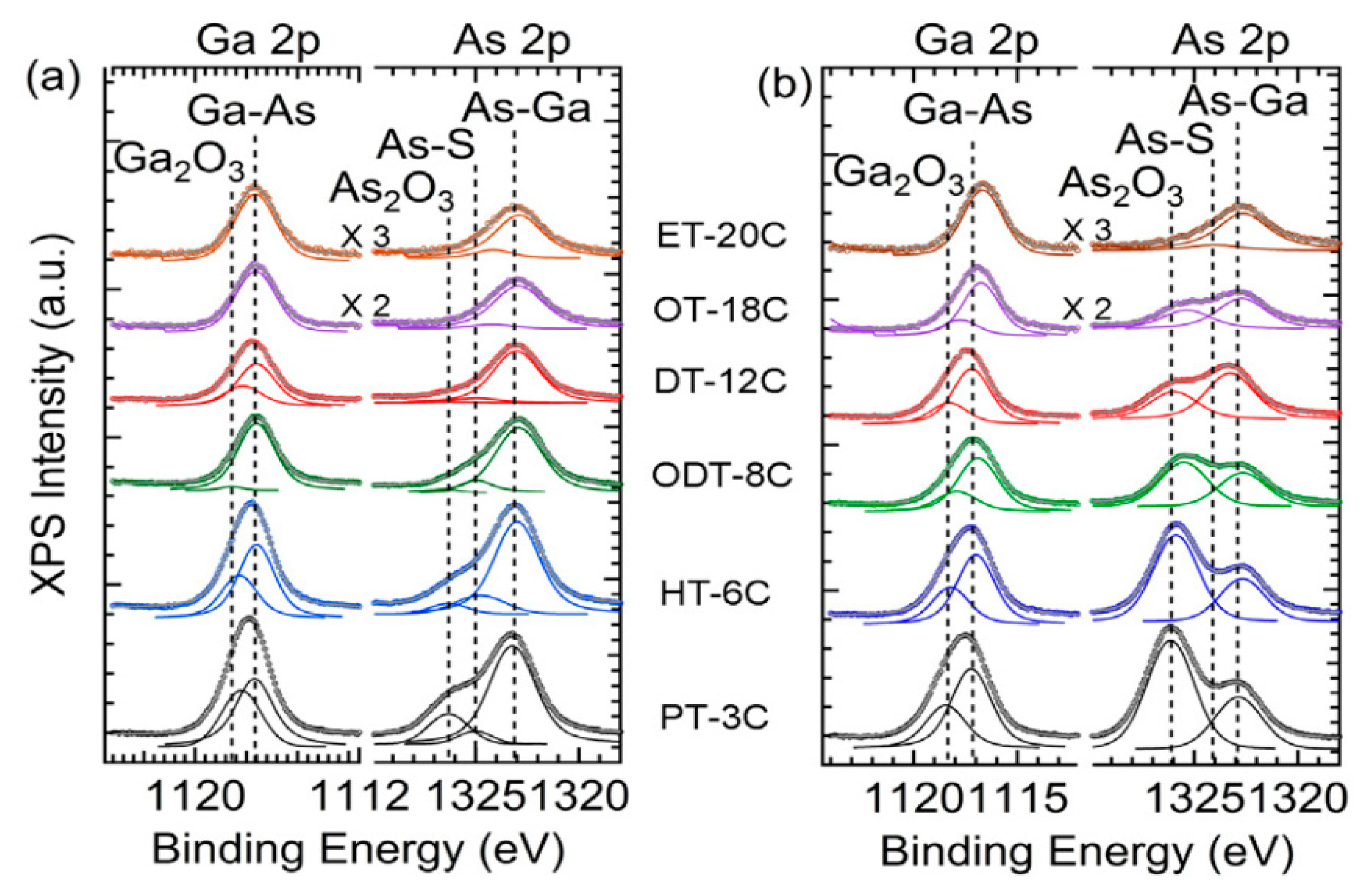
Pablo Mancheno-Posso et al. reported on the re-oxidation of the GaAs surface in the atmosphere after passivation by six alkanethiols (CnH2n+1-SH where n = 3, 6, 8, 12, 18, 20) [21]. Figure 2 shows the Ga-2p and As-2p XPS spectra after passivation by six different alkanethiols and 3/30 min of ambient exposure. We can see that, the longer alkanethiol molecule, the better stability of sulfur-passivation (for lower Ga–O and As–O signal but stronger As–S signal). In his report, the ET-20C (1-eicosanethiol, C20H41-SH) had the best passivation stability for the formation of the most ordered and highest-packing density layer, and restrained the surface re-oxidation of ambient exposure for at least 30 min.
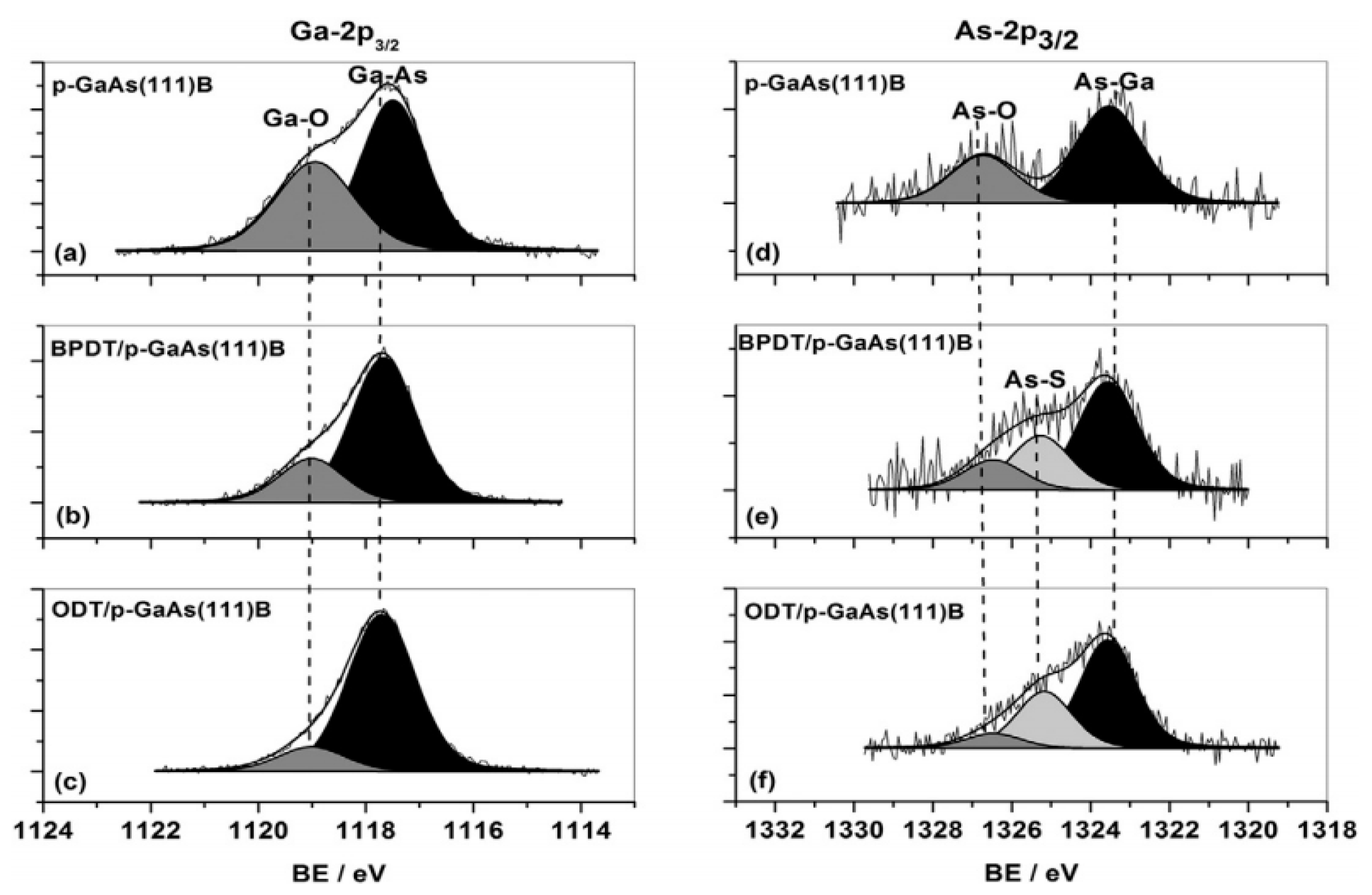
Similar results was reported by Loredana Preda et al. They investigated the effects of the SAMs of 1,8-octanedithiol (ODT) and biphenyl 4,4′-dithiol (BPDT) on the electronic and chemical properties of p-GaAs with As terminated semiconductor surface [22]. They verified that the hydrocarbon moiety had an important effect on tailoring the GaAs surface properties. The XPS spectra (Figure 3) showed that both ODT and BPDT bind to GaAs via the thiol group. Compared to the BPDT layer, the ODT layer provided better passivation protection against the reoxidation with ambient exposure. That was because the ODT molecule bound with both thiol groups to the GaAs surface, while the BPDT molecule bound with only one thiol group to the GaAs surface.
Passivation by the long-chain alkylthiol SAM have the advantage of environmental friendliness, simple process, low cost, and good treatment effect, but at the same time, needs a relatively long time (for hours) to obtain clean surfaces and well-ordered SAM, which limit its practical application in device processing.
2.2. Passivation Film Depositing by Atomic Layer Deposition (ALD) Technique
III-V compound semiconductors are regarded as promising candidates to replace the silicon channel for future MOSFETs because of their high mobility [23]. However, compared with Si-MOSFETs, the high interface defect density between high-k gate and III-V semiconductor hampers the development of III-V MOSFETs. The Fermi level pinning phenomenon, resulting from high interface defect density at the high-k/semiconductor interface, could only produce MOSFETs with very poor control of carrier flow and various instabilities such as hysteresis and drain current drift. Therefore, interface passivation became very significant for realizing a high-performance of III-V MOSFETs.
ALD is the most advanced technique for high-k gate material deposition because it offers outstanding film thickness control, pinhole-free and conformal deposition around complex structure. Using ALD for interface passivation prior to gate film deposition has the advantage of in situ processing without any vacuum breaking, which further improve the interface quality, and the “self-cleaning” process [24,25,26,27,28] can reduce and/or removal of native oxides of III-V semiconductors by surface reactions with the ALD precursors during the initial stages of deposition.
Surface passivation of III-V semiconductors using ALD-Al2O3 had been researched the most widely. As2O3 first interacts with Al (CH3)3 to be transformed to arsenic and Al2O3. The arsenic then reacts with H2O to become As2O5, which then reacts again with the next incoming pulse of Al (CH3)3 to become As and Al2O3. Most of the arsenic oxides evaporated since the melting point of As2O5 is low around 280 °C with a small amount of residual As2O5 left on the skin-depth top of Al2O3 [29].
The interaction of Al (CH3)3 with native oxides of GaAs surfaces leads to most of the surface arsenic oxides and a significant portion the gallium oxide being consumed. It seems that just a half cycle of Al2O3 could passivate the majority of the defects [24], but according to the research of Kent et al. [30], dissociative chemisorption of Al(CH3)3 was found to also lead to the formation of an ordered monolayer of dimethyl aluminum that not only passivated the As dangling bonds but also resulted in the formation of metal–metal bonds that pinned the Fermi level, so dosing with H2O or O2 was required to passivate the surface and unpin the Fermi level by inserting O atoms in the metallic bond.
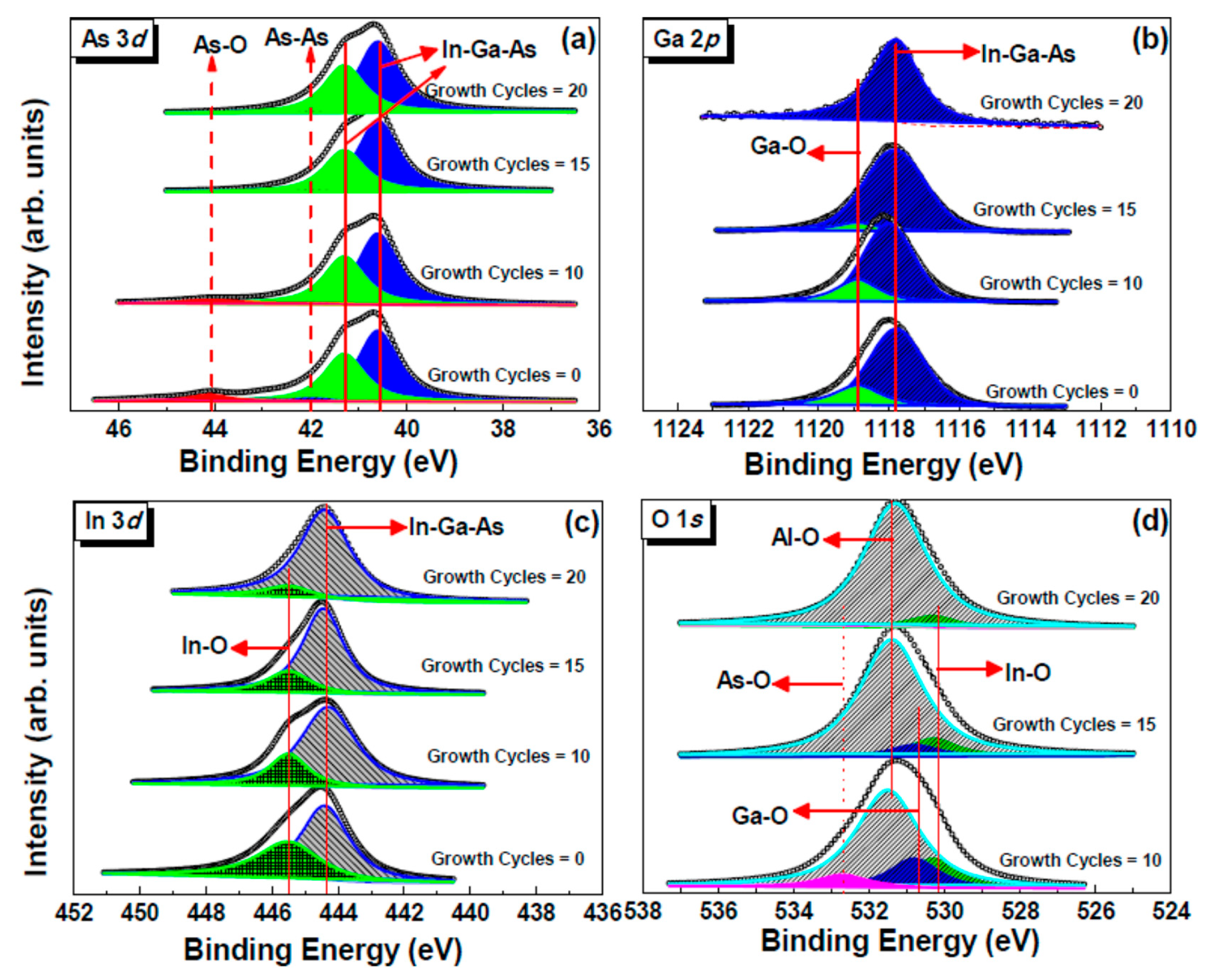
Generally, the arsenic oxides were energetically the easiest to remove and the indium oxides were hardest. Gang He et al. reported improving the interface quality in HfTiO/InGaAs metal oxide semiconductor capacitor (MOSCAP) by introducing ALD-Al2O3 passivation film [31]. XPS measurements shown in Figure 4 had confirmed that, after 20 cycles of ALD-Al2O3 passivation, none of the Ga–O and As–O bonds were detected, and significant suppressing the formation of In–O bond had been achieved. Electrical measurements of MOSCAP with HfTiO/4 nm-Al2O3/InGaAs structure indicated improved electrical characteristics were achieved.
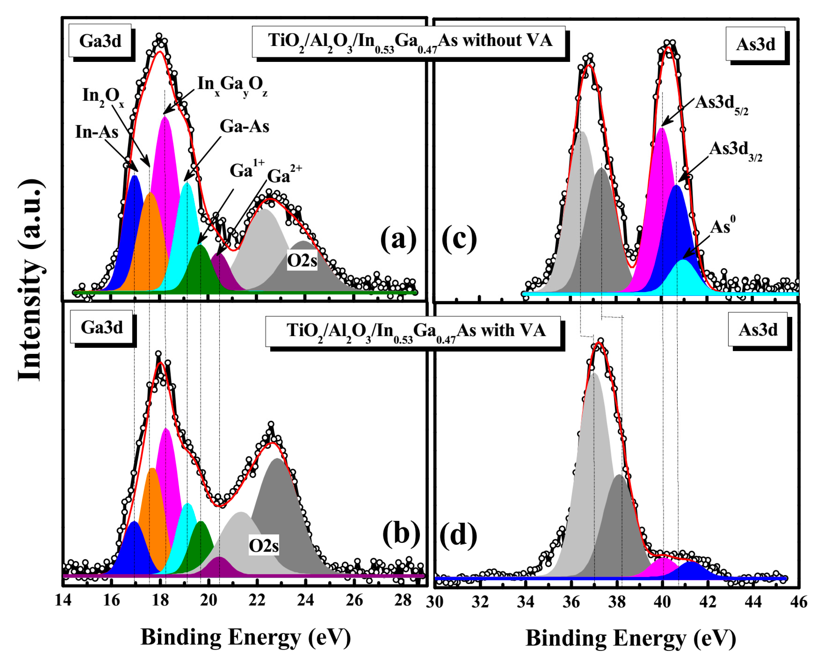
C. Mukherjee et al. put forward the bilayer of ALD-TiO2/Al2O3 structure to passivate the InGaAs MOSFETs surface and used as the gate oxide in the meanwhile [8]. TiO2 had high dielectric constant and Al2O3 was beneficial to reduce the interface defect density. It was found that the TiO2/Al2O3 structure helped to control the As out-diffusion and reduced the As–O and In–O bond on the InGaAs surface. It was shown in Figure 5 that with the action of VA (vacuum annealing) at 350 °C, all native oxides were effectively removed.
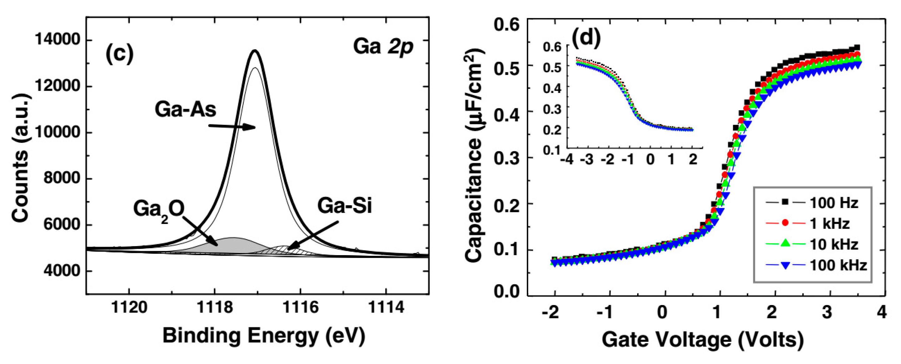
Although ALD of Al2O3 can suppress the formation of the As–O and Ga–O bonds, it seems that the self-cleaning ALD process was not sufficient to deposit a gate dielectric with a high-quality interface. For instance in Figure 6 the electrical properties of a stack consisting of 10 nm ALD Al2O3 on GaAs (100) were compared for two different surface preparations: HF etch directly and 1.2 nm Si passivation layer depositing by PECVD. In the latter case the frequency of the C-V curves was significantly reduced (as shown in Figure 6b,d). Si passivation layer at the interface resulted in gettering of oxygen from the substrate to result in a partially oxidized Si layer and the removal of all As-oxides (not shown here), as well as the higher 3+ oxidation state of Ga (as shown in Figure 6a,c). We also noted that the Ga2O bonding arrangement remains for the two interfaces suggesting that it was not the species primarily responsible for Fermi-level pinning.
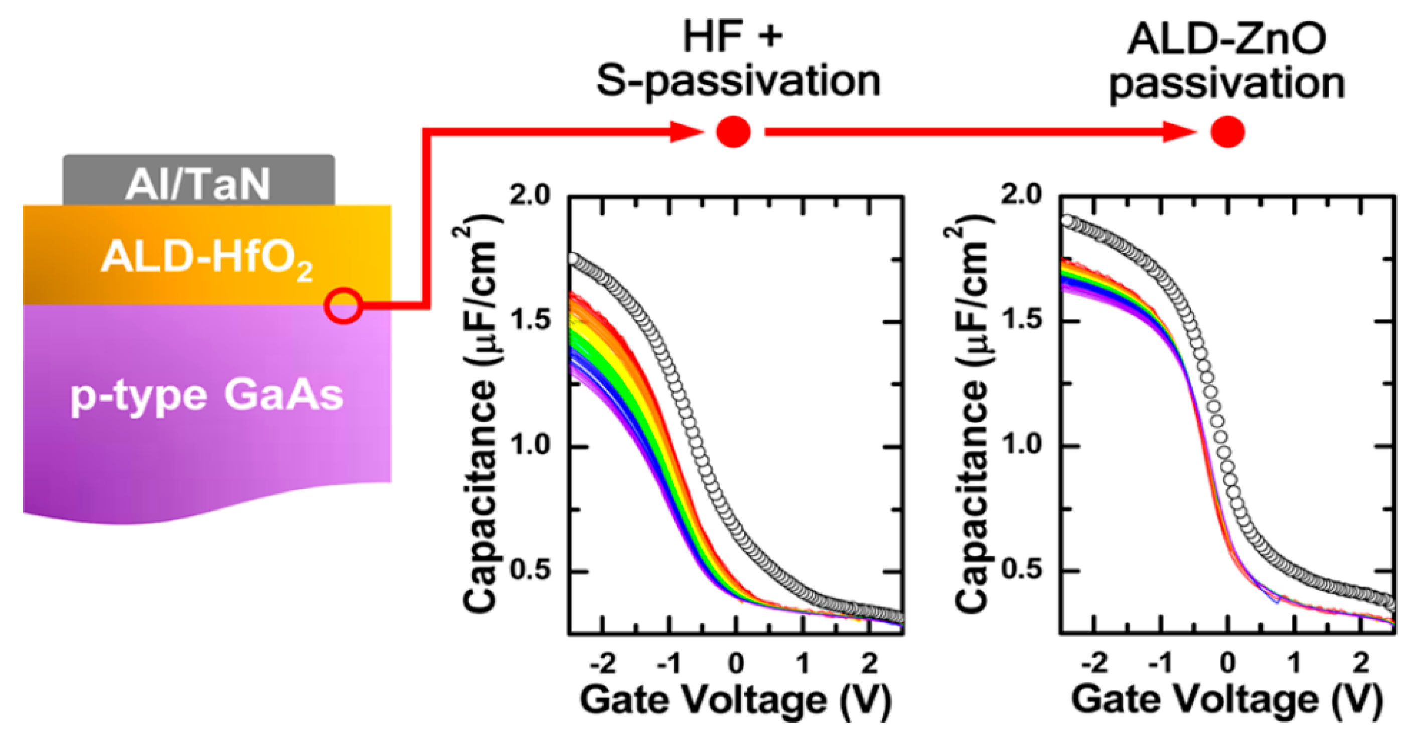
ZnO wideband material has attracted increasing attention in the passivation field. Although O atoms exist in ZnO, it is nearly impossible for ZnO to react with Ga or As for the high exciting binding energy of Zn–O bonds [33]. Young-Chul Byun et al. investigated ultrathin ZnO film by the ALD method as interface passivation layer between HfO2 gate and GaAs substrate [34]. The Ga–O bond/As segregation near the interface and the trapping of carriers near the valence band edge was significantly suppressed, greatly improving the C-V characteristics on p-type GaAs substrates, as shown in Figure 7.
Similar results were reported by Liu Chen et al. [35], who found deposition of ZnO prior to Al2O3 gate materials deposition directly can further reduce the interface trap density. The n-GaAs MOSCAP with 2 nm ALD ZnO interface passivation layer exhibited higher accumulation capacitance and a very small C–V dispersion and hysteresis. They explained the result that the presence of ZnO on n-GaAs can act as the oxygen reaction barrier and effectively reduces the Ga and As oxides, which suppresses the formation of low k interfacial layer on the GaAs surface, thus improving the interface quality and leading to higher accumulation capacitance.
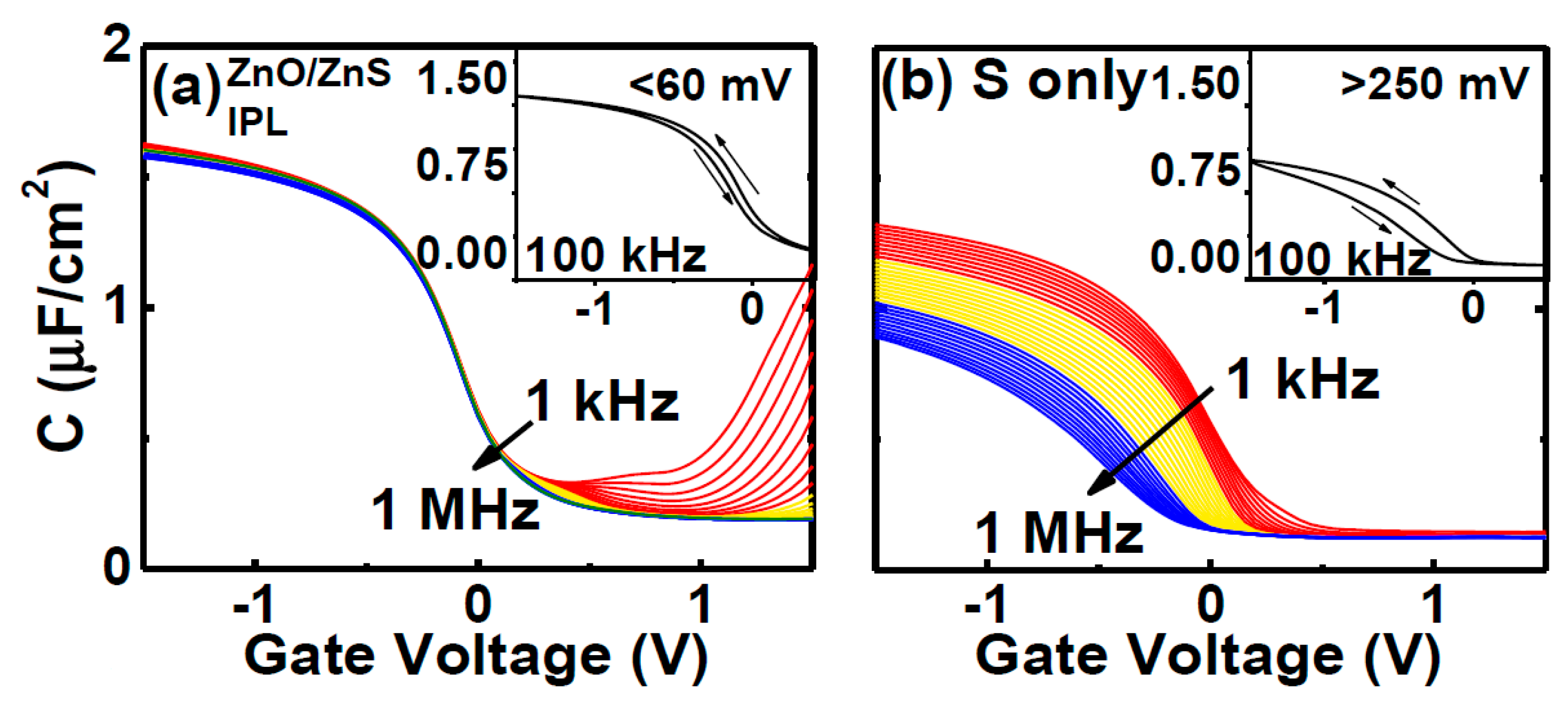
ZnS has better thermochemical stability and higher band gap energy than ZnO [36], which makes it an attractive and promising candidate as an interface passivation layer (IPL) material in III-V based devices. Lucero et al. used ALD to format a ZnO/ZnS IPL by converting an (NH4)2S cleaned p-In0.53Ga0.47As with diethylzinc and water [37]. Diethylzinc reacted with S and O on the InGaAs, reducing Ga3+ and As3+ to lower oxidation states. Measurements of C-V characteristics of HfO2-InGaAs MOSCAP in Figure 8 showed that the ZnO/ZnS bilayer nearly eliminated frequency dispersion and hysteresis.
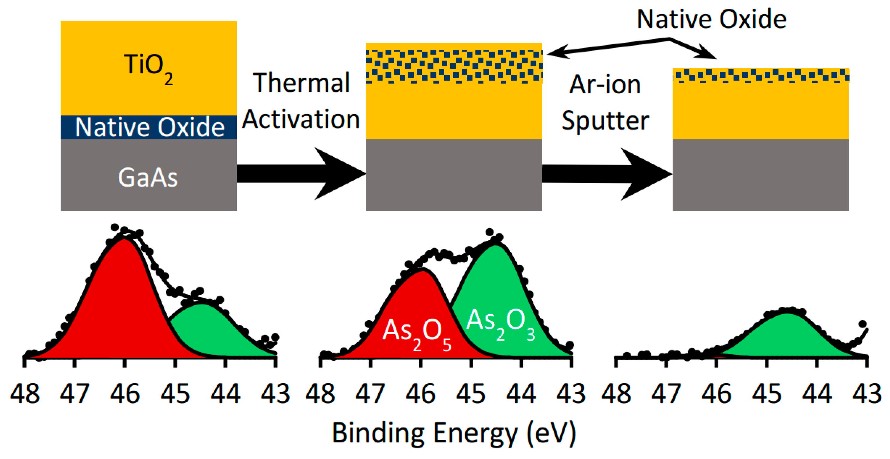
Henegar et al. reported a novel method to transport the native oxides away from the GaAs surface by ALD TiO2 film [38]. In his study, a 4 nm TiO2 film were deposited on native oxide GaAs at 100 °C firstly. The low temperature were used to limit the native oxide mobility and “clean-up” reactions. This layer protected the interfacial layer from precursor and air exposure and created a native oxide concentration gradient in the sample. Secondly, select films were heated for hours at 250 °C in the ALD reactor under N2; this thermal activation step was aimed at promoting native oxide migration into the film. Lastly, a 3 nm TiO2 were deposited at a higher temperature to remove any native oxide that may have reached the surface. The XPS confirmed the removal of the arsenic (as shown in Figure 9) and gallium oxides during the second layer of 3 nm TiO2 deposition at 150–250 °C when a large enough thermal budget was applied before and/or during the deposition. They also found that the gallium oxides were less mobile and harder to remove than arsenic oxides.
It turns out that passivation film depositing by ALD technology provides a quick and reliable way to obtain low oxygen-contaminate III-V surfaces making these cleaning methods preferable for device processing.
2.3. Plasma Treatment and Nitridation
Plasma treatment is the removal of surface oxide through the impact of highly energetic ions (e.g., Ar+, N+ [39,40,41]) or chemical reaction (e.g., NH3+, H+, HS+), then the dangling bonds are further saturated. This led to a great reduction of the surface state density. Among various plasma treatments, N-plasma passivation has gained the most extensive research and been considered a very effective way to get clean GaAs surface by terminating GaAs bonds with GaN [42,43,44].
In the report of H. H. Lu et al. [45,46], they treated GaAs MOS Capacitor with N2 and NH3 respectively at the gas flow of 4 sccm, 350 °C and power of 120 W in PECVD chamber. Both of the two plasma-passivated MOSCAP exhibited improved interfacial and electrical properties compared to the untreated one, and NH3-plasma passivated sample had the better effect than N2-plasma, which showed the lower leakage current density and interface-state density. That may be for the NH3-plasma passivation can provide additional reactive species, such as H atoms and NH radicals, than N2-plasma passivation which provided nitrogen atoms only, so leading to better removal of the elemental As, Ga–O and As–O bonds.
Seung-Hwan Kim et al. applied the novel SF6 plasma passivation technique with inserting a ultrathin ZnO IPL for the metal interlayer semiconductor (MIS) structure to alleviate the interface trap states [47]. The optimized plasma conditions had a process time of 10 s, gas flow of 10 sccm, pressure of 5 mTorr, source power of 50 W, and the ALD-ZnO thickness of 1.3 nm. The source/drain contact resistance testing in Figure 10 showed that the current density of the SF6-treated MIS contact were about 4 times and 15 times larger than that of the (NH4)2S-passivated MIS contact and non-passivated MIS contact. The result proposed a promising non-alloyed S/D ohmic contact for III-V MOS.
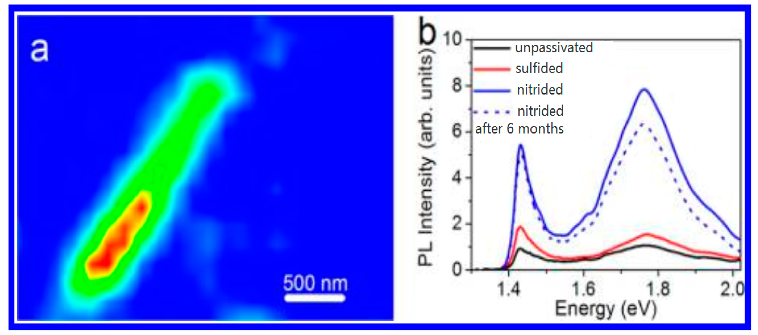
In the research of Alekseev et al. [48], surface nitridation by hydrazine-sulfide solution were used for GaAs nanowires because of the high stability of Ga–N bonds. To avoid micro-etching and prevent possible damage to the NW surface morphology, they used a low alkaline (pH ~8.5) hydrazine sulfide solution by adding anhydrous hydrazine dihydrochloride (N2H4 × 2HCl) into hydrazine hydrate and then introducing Na2S into the solution up to a concentration of 0.01 M. Figure 11 shows typical μ-PL spectra measured from unpassivated, sulfided, and nitrided NWs. They found nitridation producing an essential increase in the NW conductivity and the μ-PL intensity as well as evidence of surface passivation. Estimations showed that the nitride passivation reduced the surface state density by a factor of 6, the effects of the nitride passivation were also stable under atmospheric ambient conditions for six months.
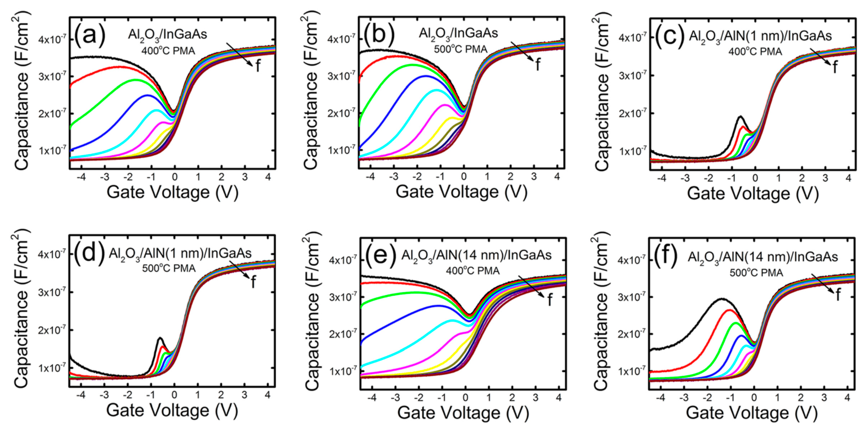
Krylov et al. [49] used oxygen-free AlN dielectric to reduce the interface state density and systematically studied the interface properties of Al2O3/AlN/InGaAs structures with different AlN thicknesses. AlN and Al2O3 films were deposited by plasma enhanced (2800 W) and thermal activated ALD techniques respectively. Frequency-dependent capacitance voltage measurements shown in Figure 12 demonstrated that the insertion of the AlN layer significantly reduced the midgap interface states density, and the indium out-diffusion phenomenon observed for Al2O3/InGaAs structures was prevented with the insertion of AlN on the top of InGaAs. High temperature annealing of 500 °C was required for interface quality improvement when thick AlN layers were used; however, stacks with ultrathin AlN layers (~1 nm) can achieve the same interface quality while using only a mild anneal of 400 °C. AlN film deposited by ALD [50], sputtering [51] or MOCVD [52] all produced the effective passivation effect.
Mary Edmonds et al. [53] reported a saturated Si–Hx capping layer deposited on InGaAs(001) surface in HV-ALD chamber by using a single Si3H8 ALD precursor at 250 °C or cyclically dosing Si2Cl6 and atomic hydrogen at 350 °C. They proved that a Si–Hx monolayer can remove all the dangling bonds and leave a charge balanced InGaAs surface.
Ultrathin passivation film especially nitride film deposition with plasma pretreatment can provide excellent contamination removal efficiency and a stable protection, but the plasma energy and film thickness should be carefully optimized to gain less roughness and a less stressed surface.
Previous technology focused on III-V semiconductor surface passivation and the testing methods are listed in Table 1.
3. Conclusions
This paper reviewed the present status of surface passivation technology for III-V semiconductors, which mainly focused on sulfur passivation by long-chain alkylthiol SAM, passivation film deposition by ALD technology, plasma treatment and nitridation. The passivation methods discussed in this paper were primarily about the microelectronics field, but these methods were also used in optoelectronic devices, which led to a low contamination III-V surface.
Long-chain alkylthiol SAM was the simplest and least expensive method, but had the drawback of being time-consuming which limit its piratical application in device processing. Plasma treatment and nitridation need to optimize the plasma energy and film thickness carefully to gain less roughness and a less stressed surface. By contrast, ALD passivation technology was efficient and easier to use, possibly making the integration of ALD passivation into the device processing easier. Many of these passivation techniques worked in the laboratory, and to improve the repeatability in the field will be the major problem.
Acknowledgments
This research was funded by the Jilin Province Science and Technology Development Plan (No. 20170520169JH, 20160204069GX and 20170101111JC), National Natural Science Foundation of China (No. 51672103 and 61774024) and National Key R&D Project (No. 2016YFB0401103 and 2017YFB0405100). Thank Selma Xin for editing this manuscript.
Conflicts of Interest
The authors declare no conflict of interest.
References
- Tajik, N.; Peng, Z.; Kuyanov, P.; LaPierre, R.R. Sulfur passivation and contact methods for GaAs nanowire solar cells. Nanotechnology 2011, 22, 225402. [Google Scholar] [CrossRef] [PubMed]
- Zhou, L.; Gao, X.; Wang, Y.; Xu, L.; Jia, B.; Bai, D.; Bo, B. Facet passivation of GaAs based LDs by plasma pretreatment and RF sputtered AlN film coating. J. Light Wave Technol. 2013, 31, 2279–2283. [Google Scholar]
- Cao, M.; Lin, Z.; Wang, S.; Li, Q.; Xiao, G.; Gao, X.; Liu, H.; Li, H. Property improvement of Al2O3-InP metal oxide semicondcutor capacitors by surface nitridation. Chin. J. Vac. Sci. Technol. 2016, 36, 7. [Google Scholar]
- Robertson, J.; Guo, Y.; Lin, L. Defect state passivation at III-V oxide interfaces for complementary metal–oxide–semiconductor devices. J. Appl. Phys. 2015, 117, 112806. [Google Scholar] [CrossRef]
- Lee, M.-K.; Yen, C.-F. Characteristics of liquid phase deposited SiO2 on (NH4)2S-treated GaAs with an ultrathin Si interface passivation layer. Jpn. J. Appl. Phys. 2014, 53, 056502. [Google Scholar] [CrossRef]
- Ghita, R.V.; Negrila, C.C.; Cotirlan, C.; Logofatu, C. On the passivation of GaAs surface by sulfide compounds. Dig. J. Nanomater. Biostruct. 2013, 8, 1335–1344. [Google Scholar]
- Jiang, S.S.; He, G.; Liang, S.; Zhu, L.; Li, W.D.; Zheng, C.Y.; Lv, J.G.; Liu, M. Modulation of interfacial and electrical properties of HfGdO/GaAs gate stacks by ammonium sulfide passivation and rapid thermal annealing. J. Alloys Compd. 2017, 704, 322–328. [Google Scholar] [CrossRef]
- Mukherjee, C.; Das, T.; Mahata, C.; Maiti, C.K.; Chia, C.K.; Chiam, S.Y.; Chi, D.Z.; Dalapati, G.K. Interface properties of atomic layer deposited TiO2/Al2O3 films on In(0.53)Ga(0.47)As/InP substrates. ACS Appl. Mater. Interfaces 2014, 6, 3263–3274. [Google Scholar] [CrossRef] [PubMed]
- Gougousi, T. Atomic layer deposition of high-k dielectrics on III–V semiconductor surface. Prog. Cryst. Growth Charact. Mater. 2016, 62, 1–21. [Google Scholar] [CrossRef]
- Hasegawa, H.; Akazawa, M. Surface passivation technology for III–V semiconductor nanoelectronics. Appl. Surf. Sci. 2008, 255, 628–632. [Google Scholar] [CrossRef]
- Hasegawa, H.; Akazawa, M.; Domanowska, A.; Adamowicz, B. Surface passivation of III–V semiconductors for future CMOS devices—Past research, present status and key issues for future. Appl. Surf. Sci. 2010, 256, 5698–5707. [Google Scholar] [CrossRef]
- Fu, Y.-C.; Peralagu, U.; Millar, D.A.J.; Lin, J.; Povey, I.; Li, X.; Monaghan, S.; Droopad, R.; Hurley, P.K.; Thayne, I.G. The impact of forming gas annealing on the electrical characteristics of sulfur passivated Al2O3/In0.53Ga0.47As (110)metal-oxide-semiconductor capacitors. Appl. Phys. Lett. 2017, 110, 142905. [Google Scholar] [CrossRef]
- Zhernokletov, D.M.; Dong, H.; Brennan, B.; Kim, J.; Wallace, R.M. Optimization of the ammonium sulfide (NH4)2S passivation process on InSb(111)A. J. Vac. Sci. Technol. B Nanotechnol. Microelectron. Mater. Process. Meas. Phenom. 2012, 30, 04E103. [Google Scholar] [CrossRef]
- Lebedev, M.V.; Kunitsyna, E.V.; Calvet, W.; Mayer, T.; Jaegermann, W. Sulfur Passivation of GaSb(100) Surfaces: Comparison of Aqueous and Alcoholic Sulfide Solutions Using Synchrotron Radiation Photoemission Spectroscopy. J. Phys. Chem. C 2013, 117, 15996–16004. [Google Scholar] [CrossRef]
- Lim, H.; Carraro, C.; Maboudian, R.; Pruessner, M.W.; Ghodssi, R. Chemical and Thermal Stability of Alkanethiol and Sulfur Passivated InP(100). Langmuir 2004, 20, 743–747. [Google Scholar] [CrossRef] [PubMed]
- McGuiness, C.L.; Shaporenko, A.; Mars, C.K.; Uppili, S.; Zharnikov, M.; Allara, D.L. Molecular self-assembly at bare semiconductor surfaces: Preparation and characterization of highly organized octadecanethiolate monolayers on GaAs(001). J. Am. Chem. Soc. 2006, 128, 5231–5243. [Google Scholar] [CrossRef] [PubMed]
- Budz, H.A.; Biesinger, M.C.; LaPierre, R.R. Passivation of GaAs by octadecanethiol self-assembled monolayers deposited from liquid and vapor phases. J. Vac. Sci. Technol. B Microelectron. Nanometer Struct. Process. Meas. Phenom. 2009, 27, 637. [Google Scholar] [CrossRef]
- Ding, X.; Moumanis, K.; Dubowski, J.J.; Tay, L.; Rowell, N.L. Fourier-transform infrared and photoluminescence spectroscopies of self-assembled monolayers of long-chain thiols on (001) GaAs. J. Appl. Phys. 2006, 99, 054701. [Google Scholar] [CrossRef]
- Ye, S.; Li, G.; Noda, H.; Uosaki, K.; Osawa, M. Characterization of self-assembled monolayers of alkanethiol on GaAs surface by contact angle and angle-resolved XPS measurements. Surf. Sci. 2003, 529, 163–170. [Google Scholar] [CrossRef]
- Cuypers, D.; Fleischmann, C.; van Dorp, D.H.; Brizzi, S.; Tallarida, M.; Müller, M.; Hönicke, P.; Billen, A.; Chintala, R.; Conard, T.; et al. Sacrificial Self-Assembled Monolayers for the Passivation of GaAs (100) Surfaces and Interfaces. Chem. Mater. 2016, 28, 5689–5701. [Google Scholar] [CrossRef]
- Mancheno-Posso, P.; Muscat, A.J. Self-assembly of alkanethiolates directs sulfur bonding with GaAs(100). Appl. Surf. Sci. 2017, 397, 1–12. [Google Scholar] [CrossRef]
- Preda, L.; Anastasescu, M.; Dobrescu, G.; Negrila, C.; Lazarescu, V. Role of the dithiolate backbone on the passivation of p-GaAs(111)B surface. J. Electroanal. Chem. 2016, 771, 56–63. [Google Scholar] [CrossRef]
- Ponath, P.; Posadas, A.B.; Demkov, A.A. Ge(001) surface cleaning methods for device integration. Appl. Phys. Rev. 2017, 4, 021308. [Google Scholar] [CrossRef]
- Milojevic, M.; Aguirre-Tostado, F.S.; Hinkle, C.L.; Kim, H.C.; Vogel, E.M.; Kim, J.; Wallace, R.M. Half-cycle atomic layer deposition reaction studies of Al2O3 on In0.2Ga0.8As (100) surfaces. Appl. Phys. Lett. 2008, 93, 202902. [Google Scholar] [CrossRef]
- Luo, X.; Rahbarihagh, Y.; Hwang, J.C.M.; Liu, H.; Du, Y.; Ye, P.D. Temporal and Thermal Stability of Al2O3-Passivated Phosphorene MOSFETs. IEEE Electron Device Lett. 2014, 35, 1314–1316. [Google Scholar] [CrossRef]
- Xuan, M.Y.; Lin, Hu.; Ye, P.D. Simplified Surface Preparation for GaAs Passivation Using Atomic Layer-Deposited High-κ Dielectrics. IEEE Trans. Electron Devices 2007, 54, 1811–1817. [Google Scholar] [CrossRef]
- Yen, C.-F.; Lee, M.-K.; Lee, J.-C. Electrical characteristics of Al2O3/TiO2/Al2O3 prepared by atomic layer deposition on (NH4)2S-treated GaAs. Solid-State Electron. 2014, 92, 1–4. [Google Scholar] [CrossRef]
- Hsueh, W.-J.; Chen, C.-Y.; Chang, C.-M.; Chyi, J.-I.; Huang, M.-L. Effects of GaSb surface preparation on the characteristics of HfO2/Al2O3/GaSb metal-oxide-semiconductor capacitors prepared by atomic layer deposition. J. Vac. Sci. Technol. A Vac. Surf. Films 2017, 35, 01B106. [Google Scholar] [CrossRef]
- Huang, M.L.; Chang, Y.C.; Chang, C.H.; Lee, Y.J.; Chang, P.; Kwo, J.; Wu, T.B.; Hong, M. Surface passivation of III-V compound semiconductors using atomic-layer-deposition-grown Al2O3. Appl. Phys. Lett. 2005, 87, 252104. [Google Scholar] [CrossRef]
- Kent, T.J.; Edmonds, M.; Chagarov, E.; Droopad, R.; Kummel, A.C. Dual passivation of GaAs (110) surfaces using O2/H2O and trimethylaluminum. J. Chem. Phys. 2013, 139, 244706. [Google Scholar] [CrossRef] [PubMed]
- He, G.; Gao, J.; Chen, H.; Cui, J.; Sun, Z.; Chen, X. Modulating the Interface Quality and Electrical Properties of HfTiO/InGaAs Gate Stack by Atomic-Layer-Deposition-Derived Al2O3 Passivation Layer. ACS Appl. Mater. Interfaces 2014, 6, 22013–22025. [Google Scholar] [CrossRef] [PubMed]
- Hinkle, C.L.; Milojevic, M.; Vogel, E.M.; Wallace, R.M. Surface passivation and implications on high mobility channel performance (Invited Paper). Microelectron. Eng. 2009, 86, 1544–1549. [Google Scholar] [CrossRef]
- Kundu, S.; Shripathi, T.; Banerji, P. Interface engineering with an MOCVD grown ZnO interface passivation layer for ZrO2–GaAs metal–oxide–semiconductor devices. Solid State Commun. 2011, 151, 1881–1884. [Google Scholar] [CrossRef]
- Byun, Y.C.; Choi, S.; An, Y.; McIntyre, P.C.; Kim, H. Tailoring the interface quality between HfO2 and GaAs via in situ ZnO passivation using atomic layer deposition. ACS Appl. Mater. Interfaces 2014, 6, 10482–10488. [Google Scholar] [CrossRef] [PubMed]
- Liu, C.; Zhang, Y.-M.; Zhang, Y.-M.; Lü, H.-L. Interfacial characteristics of Al/Al2O3/ZnO/n-GaAs MOS capacitor. Chin. Phys. B 2013, 22, 076701. [Google Scholar] [CrossRef]
- Kim, S.H.; Joo, S.Y.; Jin, H.S.; Kim, W.B.; Park, T.J. Ultrathin ZnS and ZnO Interfacial Passivation Layers for Atomic-Layer-Deposited HfO2 Films on InP Substrates. ACS Appl. Mater. Interfaces 2016, 8, 20880–20884. [Google Scholar] [CrossRef] [PubMed]
- Lucero, A.T.; Byun, Y.-C.; Qin, X.; Cheng, L.; Kim, H.; Wallace, R.M.; Kim, J. Formation of a ZnO/ZnS interface passivation layer on (NH4)2S treated In0.53Ga0.47As: Electrical and in-situ X-ray photoelectron spectroscopy characterization. Jpn. J. Appl. Phys. 2016, 55, 08PC02. [Google Scholar] [CrossRef]
- Henegar, A.J.; Cook, A.J.; Dang, P.; Gougousi, T. Native Oxide Transport and Removal During Atomic Layer Deposition of TiO2 Films on GaAs(100) Surfaces. ACS Appl. Mater. Interfaces 2016, 8, 1667–1675. [Google Scholar] [CrossRef] [PubMed]
- Losurdo, M.; Capezzuto, P.; Bruno, G.; Perna, G.; Capozzi, V. N2–H2 remote plasma nitridation for GaAs surface passivation. Appl. Phys. Lett. 2002, 81, 16–18. [Google Scholar] [CrossRef]
- Naritsuka, S.; Mori, M.; Takeuchi, Y.; Maruyama, T. X-ray Photoemission Spectroscopy Study of GaAs(111)B Substrate Nitridation using an RF-Radical Source. Jpn. J. Appl. Phys. 2012, 51, 048004. [Google Scholar] [CrossRef]
- Guo, Y.; Lin, L.; Robertson, J. Nitrogen passivation at GaAs:Al2O3 interfaces. Appl. Phys. Lett. 2013, 102, 091606. [Google Scholar] [CrossRef]
- Anantathanasarn, S.; Ootomo, S.-y.; Hashizume, T.; Hasegawa, H. Surface passivation of GaAs by ultra-thin cubic GaN layer. Appl. Surf. Sci. 2000, 159–160, 456–461. [Google Scholar] [CrossRef]
- Monier, G.; Bideux, L.; Robert-Goumet, C.; Gruzza, B.; Petit, M.; Lábár, J.L.; Menyhárd, M. Passivation of GaAs(001) surface by the growth of high quality c-GaN ultra-thin film using low power glow discharge nitrogen plasma source. Surf. Sci. 2012, 606, 1093–1099. [Google Scholar] [CrossRef]
- Losurdo, M. Study of the mechanisms of GaN film growth on GaAs surfaces by thermal and plasma nitridation. J. Vac. Sci. Technol. B Microelectron. Nanometer Struct. Process. Meas. Phenom. 1998, 16, 2665. [Google Scholar] [CrossRef]
- Lu, H.H.; Xu, J.P.; Liu, L.; Wang, L.S.; Lai, P.T.; Tang, W.M. Improved interfacial quality of GaAs metal-oxide-semiconductor device with NH3-plasma treated yittrium-oxynitride as interfacial passivation layer. Microelectron. Reliab. 2015, 56, 17–21. [Google Scholar] [CrossRef]
- Liu, C.-W.; Xu, J.-P.; Liu, L.; Lu, H.-H. High-k gate dielectric GaAs MOS device with LaON as interlayer and NH3-plasma surface pretreatment. Chin. Phys. B 2015, 24, 127304. [Google Scholar] [CrossRef]
- Kim, S.-H.; Kim, G.-S.; Kim, S.-W.; Kim, J.-K.; Choi, C.; Park, J.-H.; Choi, R.; Yu, H.-Y. Non-Alloyed Ohmic Contacts on GaAs Using Metal-Interlayer-Semiconductor Structure With SF6 Plasma Treatment. IEEE Electron Device Lett. 2016, 37, 373–376. [Google Scholar] [CrossRef]
- Alekseev, P.A.; Dunaevskiy, M.S.; Ulin, V.P.; Lvova, T.V.; Filatov, D.O.; Nezhdanov, A.V.; Mashin, A.I.; Berkovits, V.L. Nitride Surface Passivation of GaAs Nanowires: Impact on Surface State Density. Nano Lett. 2014, 15, 63–68. [Google Scholar] [CrossRef] [PubMed]
- Krylov, I.; Pokroy, B.; Ritter, D.; Eizenberg, M. Passivation of InGaAs interface states by thin AlN interface layers for metal-insulator-semiconductor applications. J. Vac. Sci. Technol. B Nanotechnol. Microelectron. Mater. Process. Meas. Phenom. 2017, 35, 011205. [Google Scholar] [CrossRef]
- Weiland, C.; Rumaiz, A.K.; Price, J.; Lysaght, P.; Woick, J.C. Passivation of In0.53Ga0.47As/ZrO2 interfaces by AlN atomic layer deposition process. J. Appl. Phys. 2013, 114, 034107. [Google Scholar] [CrossRef]
- Gao, F.; Lee, S.J.; Kwong, D.L. Enhancement mode GaAs metal-oxide-semiconductor field-effect-transistor integrated with thin AlN surface passivation layer and silicon/phosphorus coimplanted source/drain. J. Vac. Sci. Technol. B Microelectron. Nanometer Struct. Process. Meas. Phenom. 2009, 27, 214. [Google Scholar] [CrossRef]
- Aoki, T.; Fukuhara, N.; Osada, T.; Sazawa, H.; Hata, M.; Inoue, T. Nitride passivation reduces interfacial traps in atomic-layer-deposited Al2O3/GaAs (001) metal-oxide-semiconductor capacitors using atmospheric metal-organic chemical vapor deposition. Appl. Phys. Lett. 2014, 105, 033513. [Google Scholar] [CrossRef]
- Edmonds, M.; Kent, T.; Chagarov, E.; Sardashti, K.; Droopad, R.; Chang, M.; Kachian, J.; Park, J.H.; Kummel, A. Passivation of InGaAs(001)-(2 × 4) by Self-Limiting Chemical Vapor Deposition of a Silicon Hydride Control Layer. J. Am. Chem. Soc. 2015, 137, 8526–8533. [Google Scholar] [CrossRef] [PubMed]
Figure 1.
GaAs surface after thermal desorption of the sacrificial SAM. (a) The overview SRPES spectrum indicates low O and C surface contamination. The (b) As 3d and (c) Ga 3d spectra also demonstrate the absence of surface oxides above the detection limit. (d) The valence band spectrum indicates the absence of strong band bending near the surface. Reproduced with permission from [20], copyright American Chemical Society (2016).

Figure 2.
The Ga-2p and As-2p X-ray photoelectron spectroscopy (XPS) spectra for GaAs passivated by six alkanethiols after (a) 3 min and (b) 30 min of ambient exposure. Reproduced with permission from [21], copyright Elsevier B. V. (2016).
Figure 2.
The Ga-2p and As-2p X-ray photoelectron spectroscopy (XPS) spectra for GaAs passivated by six alkanethiols after (a) 3 min and (b) 30 min of ambient exposure. Reproduced with permission from [21], copyright Elsevier B. V. (2016).

Figure 3.
XPS spectra of Ga-2p and As-2p for p-GaAs substrate exposed to ambient after etching (a,d), BPDT passivation (b,e) and ODT passivation (c,f). Reproduced with permission from [22], copyright Elsevier B. V. (2016).
Figure 3.
XPS spectra of Ga-2p and As-2p for p-GaAs substrate exposed to ambient after etching (a,d), BPDT passivation (b,e) and ODT passivation (c,f). Reproduced with permission from [22], copyright Elsevier B. V. (2016).

Figure 4.
XPS spectra of As 3d (a), Ga 2p (b), In 3d (c) and O 1s (d) with the influence of ALD-Al2O3 growth cycles. Reproduced with permission from [31], copyright American Chemical Society (2016).
Figure 4.
XPS spectra of As 3d (a), Ga 2p (b), In 3d (c) and O 1s (d) with the influence of ALD-Al2O3 growth cycles. Reproduced with permission from [31], copyright American Chemical Society (2016).

Figure 5.
XPS spectra of Ga 3d (a,b) and As 3d (c,d) from TiO2/Al2O3/In0.53Ga0.47As structure without and with vacuum annealing (VA). Reproduced with permission from [8], copyright American Chemical Society (2016).
Figure 5.
XPS spectra of Ga 3d (a,b) and As 3d (c,d) from TiO2/Al2O3/In0.53Ga0.47As structure without and with vacuum annealing (VA). Reproduced with permission from [8], copyright American Chemical Society (2016).

Figure 6.
(a) Ex situ XPS analysis after HF-last GaAs with overlying 1.0 nm Al2O3 layer by ALD, (b) C-V characteristics of (a) after an additional 9.0 nm Al2O3 deposition, (c) ex situ XPS analysis after HF-last GaAs with overlying 1.2 nm Si by PECVD and 1.0 nm Al2O3 layer by ALD, and (d) C-V characteristics of (c) after an additional 9.0 nm Al2O3 deposition. Reproduced with permission from [32], copyright Elsevier B. V. (2009).


Figure 7.
The C-V characteristics of HF+ (NH4)2S cleaned HfO2/p-GaAs MOSCAP with and without 10 cycle ALD–ZnO passivation layer. Reproduced with permission from [34], copyright American Chemical Society (2014).
Figure 7.
The C-V characteristics of HF+ (NH4)2S cleaned HfO2/p-GaAs MOSCAP with and without 10 cycle ALD–ZnO passivation layer. Reproduced with permission from [34], copyright American Chemical Society (2014).

Figure 8.
C-V characteristics of (NH4)2S cleaned HfO2/p-InGaAs MOSCAP with (a) and without (b) ZnO/ZnS IPL. Reproduced with permission from [37], copyright The Japan Society of Applied Physics (2016).
Figure 8.
C-V characteristics of (NH4)2S cleaned HfO2/p-InGaAs MOSCAP with (a) and without (b) ZnO/ZnS IPL. Reproduced with permission from [37], copyright The Japan Society of Applied Physics (2016).

Figure 9.
Schematic illustrating the experimental steps used to decouple the native oxide transport and removal processes. Reproduced with permission from [38], copyright American Chemical Society (2016).
Figure 9.
Schematic illustrating the experimental steps used to decouple the native oxide transport and removal processes. Reproduced with permission from [38], copyright American Chemical Society (2016).

Figure 10.
(a) I-V characteristics and (b) specific contact resistivity for metal semiconductor (MS) contact and MIS contacts. The ZnO is used as interlayer and 1.3 nm ZnO is considered the optimal thickness in both MIS contacts. Insets in (a) show a band diagram of the MIS contact (left) and a schematic of the electrical measurements of the MIS contact (right). Reproduced with permission from [47], copyright IEEE (2016).

Figure 11.
(a) μ-PL intensity distribution over the surface of nitrided n-GaAs NW; (b) μ-PL spectra taken from the middle section of the nitrided, sulfided, and unpassivated NWs. A μ-PL spectrum from a nitrided NW measured after six months of storage in ambient air is also presented. Reproduced with permission from [48], copyright American Chemical Society (2015).

Figure 12.
Typical capacitance-voltage characteristics at 400 Hz–1 MHz frequency range of (a,b) Au/Cr/Al2O3 (18 nm)/InGaAs; (c,d) Au/Cr/Al2O3 (17 nm)/AlN (1 nm)/InGaAs and (e,f) Au/Cr/Al2O3 (4 nm)/AlN (14 nm)/InGaAs gate stacks measured after annealing at 400 °C (a,c,e) and at 500 °C (b,d,e) in N2 for 5 min. Reproduced with permission from [49], copyright AIP (2017).


Table 1.
Summary of all reviewed passivation methods. (×: does not apply).
| Material | Passivation Method | Testing | Advantages | Disadvantages | Reference | |
|---|---|---|---|---|---|---|
| GaAs | ODT | XPS, AFM | Clean and smooth surfaces; Simple | Long processing time | [16,22] | |
| XPS, PL | [17,20] | |||||
| HDT | ATR-FTIR, PL | [18] | ||||
| ODT+(NH4)2S | SEM, XPS | [6] | ||||
| CnH2n+1, n ≥ 12 | XPS | [19,21] | ||||
| ALD-Al2O3 | C-V, AFM | In situ processing | Possible suboxides residues | [26,27] | ||
| Drain Current | [25] | |||||
| AlN | Sputter | C-V | Environmental friendly | × | [51] | |
| MOCVD | SIMS, C-V | Well Reliability | Complex equipment | [52] | ||
| ZnO | MOCVD | C-V, XPS, FIRTEM | [33] | |||
| ALD | XPS, SIMS, C-V | In situ processing | × | [34] | ||
| +ZnS/ZnO | C-V, XPS | Clean surfaces | [37] | |||
| +Annealing | C-V, XPS | Simple | AsOx residues | [7] | ||
| NH3 Plasma | +LaON | C-V, I-V, XPS | Well removal of Ga/As oxides. | × | [46] | |
| +YON | [45] | |||||
| N2-H2 plasma | XPS | Lower As traps | Need to be carefully optimized | [39] | ||
| N2 plasma | XPS | Well stability | [40,41,42,43,44] | |||
| SF6+ZnO | XPS, C-V | Well thermal stability | Possible GaF3 residues | [47] | ||
| ALD-TiO2+Anneal | FTIR, XRD | Extremely clean | Complex | [38] | ||
| N2H4+Na2S | μ-PL | Stable effects | × | [48] | ||
| InGaAs | (NH4)2S+Annealing | C-V | Simple | Inefficient passivate the states close to VBM | [12] | |
| ALD | -AlN | TEM, C-V, XPS | In situ processing | High temperature annealing is required | [49,50] | |
| -SiHx, Si | XPS STM | High surface uniformity | × | [32,53] | ||
| -Al2O3 | C-V, XPS | In situ processing | Possible suboxides residues | [24,29,31] | ||
| -TiO2/Al2O3 | XPS, C-V, SIMS | [8] | ||||
| GaSb | ALD-Al2O3 | AFM, XPS, C-V | [28] | |||
| (NH4)2S+2-propanol | XPS, PL | Low C signal | Possible oxide residues | [14] | ||
| InP | ALD-ZnS | XPS, TEM, C-V | In situ processing | × | [36] | |
| N2 Plasma | C-V | [3] | ||||
| ODT | XPS, AFM | Simple | Long processing time | [15] | ||
| InSb | (NH4)2S | XPS, AFM | [13] | |||
© 2018 by the authors. Licensee MDPI, Basel, Switzerland. This article is an open access article distributed under the terms and conditions of the Creative Commons Attribution (CC BY) license (http://creativecommons.org/licenses/by/4.0/).
Share and Cite
MDPI and ACS Style
Zhou, L.; Bo, B.; Yan, X.; Wang, C.; Chi, Y.; Yang, X. Brief Review of Surface Passivation on III-V Semiconductor. Crystals 2018, 8, 226. https://doi.org/10.3390/cryst8050226
AMA Style
Zhou L, Bo B, Yan X, Wang C, Chi Y, Yang X. Brief Review of Surface Passivation on III-V Semiconductor. Crystals. 2018; 8(5):226. https://doi.org/10.3390/cryst8050226
Chicago/Turabian StyleZhou, Lu, Baoxue Bo, Xingzhen Yan, Chao Wang, Yaodan Chi, and Xiaotian Yang. 2018. "Brief Review of Surface Passivation on III-V Semiconductor" Crystals 8, no. 5: 226. https://doi.org/10.3390/cryst8050226
Note that from the first issue of 2016, this journal uses article numbers instead of page numbers. See further details here.