Article

Effect of Lithium Doping on Microstructural and Optical Properties of ZnO Nanocrystalline Films Prepared by the Sol-Gel Method

1
Department of Electronic Engineering, Ming Chi University of Technology, No. 84 Gongzhuan Road, New Taipei City 24301, Taiwan
2
Department of Electronic Engineering, National Changhua University of Education, No. 2, Shi-Da Road, Changhua 50074, Taiwan
3
Department of Electronic Engineering, Hsiuping University of Science and Technology, No.11 Gongye Road, Taichung 41280, Taiwan
*
Author to whom correspondence should be addressed.
Crystals 2018, 8(5), 228; https://doi.org/10.3390/cryst8050228
Submission received: 28 April 2018 / Revised: 16 May 2018 / Accepted: 16 May 2018 / Published: 19 May 2018
(This article belongs to the Special Issue Functional Oxide Based Thin-Film Materials)

Abstract

:
The Zn1−xLixO (x = 0, 0.01, 0.03, and 0.05) nanocrystalline films were synthesized on silicon (Si) substrates by using the sol-gel method. The crystal structure and surface morphology of these films were investigated by X-ray diffraction (XRD) and field emission scanning electron microscopy (FE-SEM). We observed that the average grain size was gradually reduced with increasing doping Li content. Photoluminescence (PL) spectra show that increasing the Li content will deteriorate the crystalline quality and result in the decrease of ultraviolet emission from the excitonic recombination and the enhancement of visible emission from the recombination between the intrinsic defects. The current-voltage properties of Zn1−xLixO nanocrystalline films were also studied under dark and photo-illumination for photo-detection applications. The normalized photo-to-dark-current ratio (Iphoto − Idark)/Idark has been enhanced from 315 to 4161 by increasing the Li content of the Zn1−xLixO nanocrystalline films from zero to 0.05.

1. Introduction

Wide band gap materials with transparent properties are important for photovoltaic and optoelectronic devices. Zinc oxide (ZnO) is one of the attractive transparent compound semiconductor materials with wide band gap (3.3 eV) and a large exciton binding energy (60 meV) at room temperature [1,2]. Due to its specific properties, ZnO-based optoelectronic devices are believed to be promising candidates for transparent electronics applications [3], such as in thin film transistors [4,5,6], solar cells [7,8], photodetectors, [9] and light emitting devices [10]. Furthermore, due to its high electromechanical coupling coefficients, ZnO can be used in surface acoustic wave devices and chemical biosensors [11]. ZnO crystals or films have been successfully prepared by various kinds of fabrication methods, such as Radio Frequency (RF) magnetic sputtering, chemical vapor deposition, pulsed laser deposition, and sol-gel methods. Those fabricating systems require high vacuum and complicated temperature control processes, while the sol-gel process offers more merits due to ease of control of the chemical composition and a much simpler method for large-area coating at a low cost [12]. To realize an electronic device consisting of p- and/or n-type characteristics, the doping technique is an important issue. Until now, several studies on ZnO doped with group III elements [13,14,15], transition metals [16,17], and other elements [18,19] have been explored. The dopants may not only change the dominant crystal orientation, but also play an important role in the enhancement of the photo-to-dark-current ratio via the doping-induced defect states [20]. However, it is difficult to achieve good and reproducible p-type ZnO due to low solubility of the dopant and high self-compensation [21]. The p-type ZnO was reported by doping Li since the solubility of Li in ZnO can be up to 30% [22]. The interest in using Li as the dopant in ZnO is based on its potential ability to act as a p-type dopant and ferroelectricity behavior as reported in II–VI semiconductors [23]. Due to its specific and interesting properties, further study of the microstructural and optical properties of lithium doping on of ZnO is not only thought-provoking, but also important.
In this paper, we report a study of the doping effect of Li atoms on the optical and structural properties of Zn1−xLixO (x = 0, 0.01, 0.03, and 0.05) nanocrystalline films. The X-ray diffraction (XRD) and field emission scanning electron microscopy (FESEM) were used to characterize the crystal structure and surface morphology of Zn1−xLixO nanocrystalline films. The emission behaviors were probed by the photoluminescence (PL) technique. In addition, we also carried out the current-voltage (I–V) measurements under dark and UV illumination to investigate their optical detection properties.

2. Experimental

The source solutions for the growth of Zn1−xLixO nanocrystalline films were prepared with the precursors of zinc acetate dihydrate (CH3COO)2 Zn·2H2O and lithium acetate dehydrate C2H3LiO2·2H2O which were dissolved in stoichiometric proportions in deionized water. The concentration of metal ions was kept at 0.5 M with lithium mole ratios of 0%, 1%, 2%, 3%, and 5%, respectively. We added ethanolamine into the solutions to obtain stable precursor solutions. After stirring at 150 °C for 1 h on a hotplate, we can obtain transparent solutions for crystal growth. A standard substrate cleaning process using ethanol (95% purity), acetone (99.87% purity), isopropyl alcohol (99.9% purity), hydrochloric acid (36% purity) and deionized water was done before crystal growth. Then, the Si substrates were rinsed in deionized water and dried by flowing nitrogen gas. Each layer was grown on the Si substrate by a spin coater with three steps: the first step with spinning rate = 100 rpm for 10 s, then the second step with a spinning rate of 3000 rpm for 30 s, then setting the preheating temperature at 300 °C for 2 mins. Ten layers were stacked on Si substrates. Then, the samples were annealed at 600 °C for 2 min by rapid thermal annealing (RTA) treatment with a heating rate of 600 °C/min.
The XRD patterns were studied by using Rigaku D/max-2200 X-ray diffractometer with Cu-Kα radiation. The surface morphology and cross-sectional views of Zn1−xLixO nanocrystalline films were investigated by field emission scanning electron microscopy (FE-SEM, HITACHI S-4800) at 3.0 kV. For PL measurements, room temperature photoluminescence (RTPL) spectroscopy was used to measure optical emissions by an He-Cd laser with a wavelength of 325 nm. In I–V characteristics, the samples were measured under dark and UV lamp illumination (365 nm) by an HP 4145 semiconductor parameter analyzer in an applied voltage from −5 to +5 V.

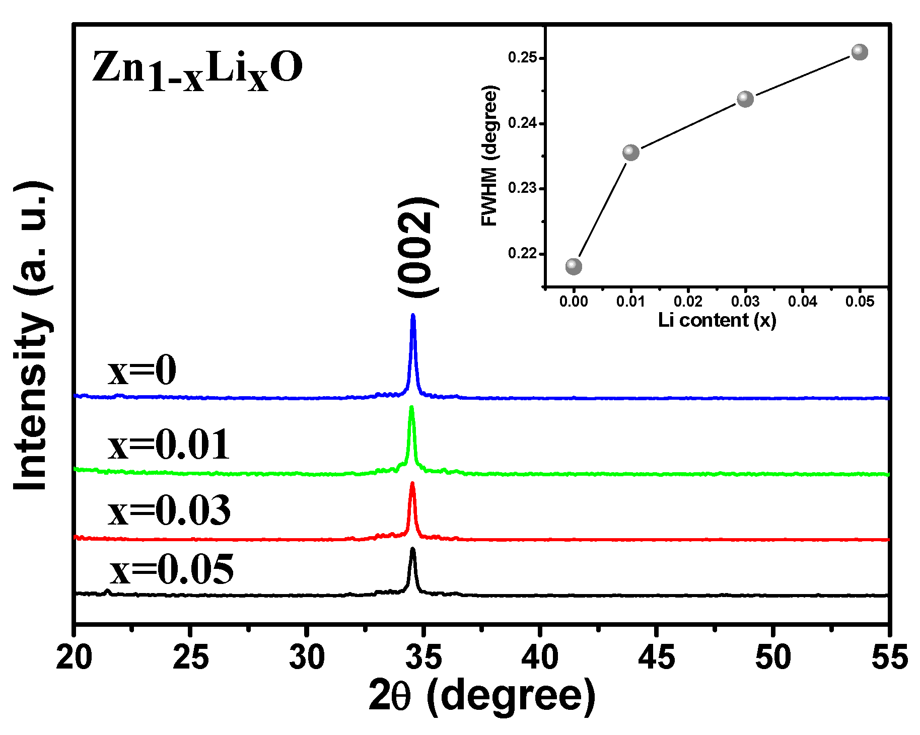
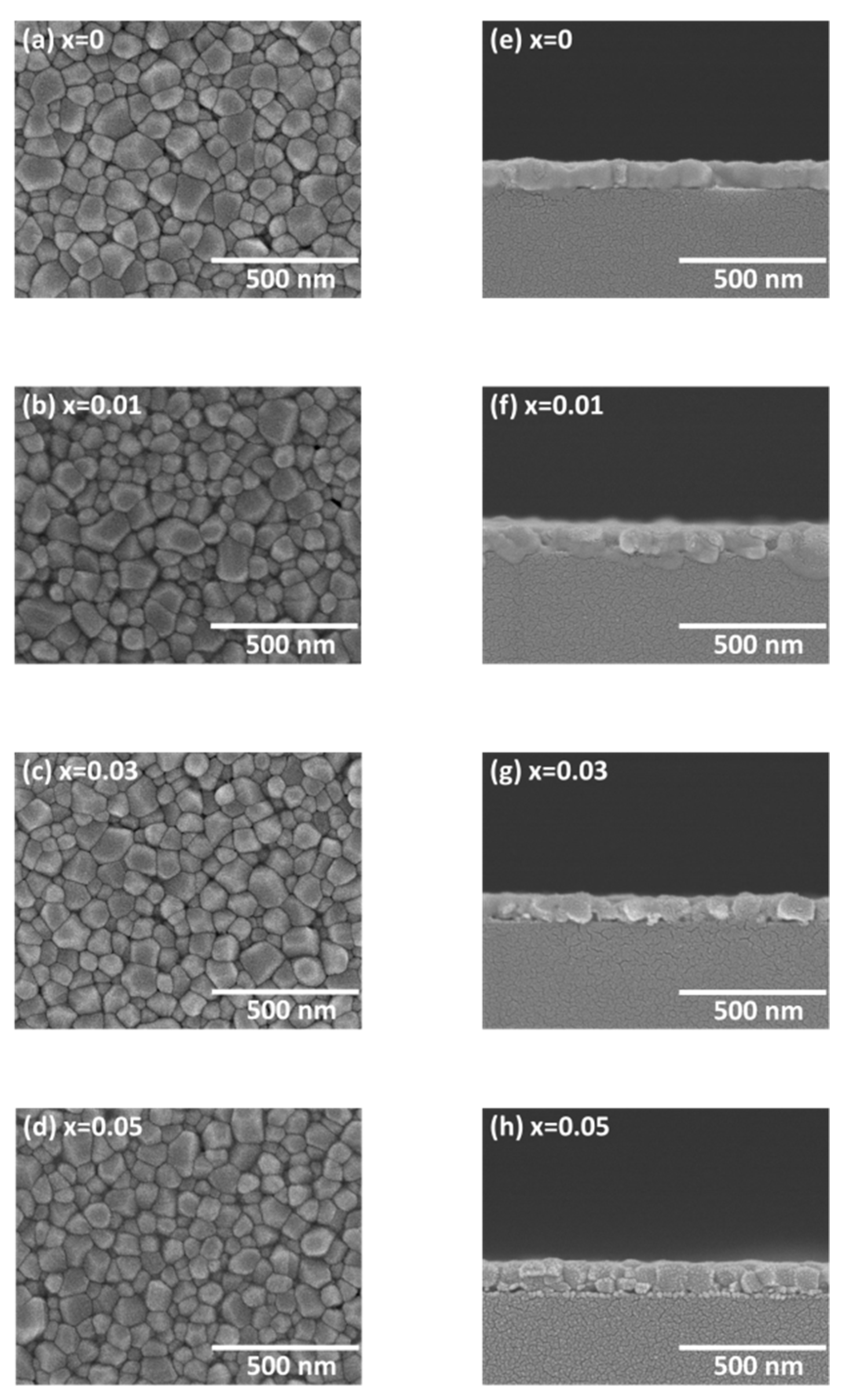
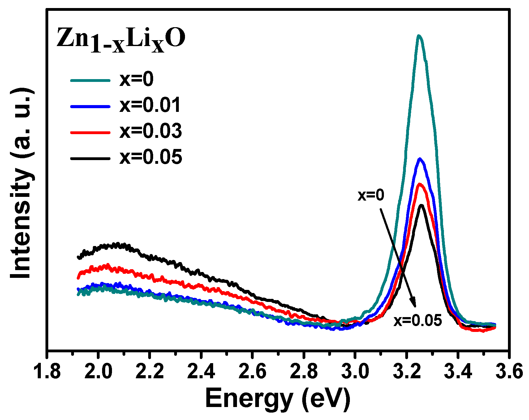
3. Results and Discussion

Figure 1 depicts the XRD patterns of Zn1−xLixO nanocrystalline films with different Li contents from x = 0 to 0.05. It is clear from observations that only one main peak located at 2θ = 34.56 degree, which demonstrates that all the Zn1−xLixO nanocrystalline films consisted of a unique phase. The Zn1−xLixO nanocrystalline film is well crystallized in a wurtzite structure with a (002) preferred orientation in the direction parallel to the c-axis. The lattice constant of c-axis can be extracted to be 5.2069 Å. E. Nurfani et al. have reported that Ti dopants change the dominant crystal orientation from (002) to (103), and also slightly extend the c-axis of the ZnO lattice parameter [20]. The results obtained in this work show that the doping of Li atoms does not cause obvious structure changes or lattice extensions. This might be due to the fact that the radii of Ti2+ or Ti4+ ions are larger than those of Li+ ions, because the atomic number of Ti is 22 while that of Li is only 3. The inset presents the full width at half maximum (FWHM) values of the XRD peaks in a function of Li content. It is noticed that the intensity of the (002) peaks gradually decreases with increasing Li content, at the same time, the FWHM are constantly broadened. We also deduced the crystallite size of Zn1−xLixO nanocrystalline films from the Debye–Scherrer’s equation [24,25] D = k λ / β cos θ , where k is the Scherer constant (k = 0.9), λ is the wavelength of the X-ray radiation (0.154 nm), β is the FWHM in radians, and θ is the Bragg diffraction angle. The results are 39.8, 36.9, 35.6, and 34.6 nm for x = 0, 0.01, 0.03, 0.05, respectively. The crystallite size is decreasing, which is due to the crystalline quality deteriorating by increasing the doping concentration of the Li atoms.
The grain size of Zn1−xLixO nanocrystalline films can also be observed by FE-SEM. Figure 2 shows both the surface morphology and cross-sectional views of Zn1−xLixO nanocrystalline films. From the top view of Zn1−xLixO nanocrystalline surface morphology, the average grain size is determined to be 88.02 to 71.16 nm for x = 0 to 0.05, respectively, and it is observed that the average grain size is gradually reduced with increasing Li doping concentration. The tendency of grain change further confirms the observation in the XRD patterns. It is noted that the crystallite size is supposed to be the size of a coherently diffracting domain and is not exactly to be the same as the particle size [26] Furthermore, it has been found that the XRD peak can be widened by defects or internal stress, so the mean crystallite size calculated by the Debye–Scherrer’s equation is smaller than the actual value [27]. In the side views, we can observe that the films are quite uniform with thicknesses of about 100 nm for all samples, and the pictures further confirm the c-axis orientation with columnar grains running perpendicular to the substrate.
Figure 3 presents the PL spectra of Zn1−xLixO nanocrystalline films for x = 0 to 0.05 taken at room temperature. The PL spectra consist of an ultraviolet (UV) emission peak and a weak green yellow visible (VIS) emission band. The sharp UV emission peaks resulted from the exciton recombination [28,29]. It is obvious that the PL intensity decreases with increasing Li doping concentration, which indicates that the doping Li atoms will deteriorate the crystalline quality. All the UV emission peaks seem located around 3.24 eV, and in careful observation we can find a slight blue shift with increasing Li doping concentration. The broader VIS emission below 2.4 eV with a peak around 2.1 eV reflects the characteristic luminescence associated with singly ionized defects, such as oxygen vacancy or doping-induced defects [30,31] Comparing the intensity of the UV emission to the VIS emission, we observe the ratio of IUV/IVIS is 8.68, 4.21, 2.52, and 1.54 for various Li doping concentrations (x = 0, 0.01, 0.03, and 0.05, respectively). We believe that the doping Li atoms are responsible for the decreasing ratio of IUV/IVIS.
Furthermore, we study the optical properties of these thin films by means of I–V curves under dark and UV illumination. The photocurrent was measured by a 30-W Xe lamp with the incident wavelength of 365 nm as the irradiation source. In Figure 4, the I–V curves of Zn1−xLixO nanocrystalline films were measured under dark and UV illumination in the voltage range from −5 to +5 V. For optical detection applications, the relative optical response can be defined by the normalized photo-to-dark-current ratio (Iphoto − Idark)/Idark. The results at +5 V are calculated and listed in Table 1. This shows that the doping Li atoms are helpful to enhance the ratio of (Iphoto − Idark)/Idark, which has been raised more than ten times from 315 to 4161.

4. Conclusions

The ZnO doped with Li (0–5%) was successfully synthesized by the sol-gel method. XRD patterns showed a single crystalline phase of Zn1−xLixO. The composition-dependent crystallite size was deduced by Debye–Scherrer’s equation, and further confirmed by the surface morphology from FE-SEM images. The PL spectra show a slight blue shift with an increase in Li content. The intensity of UV emission from exciton recombination decreases with increasing Li content, which is due to crystalline deterioration. The higher ratio of the normalized photo-to-dark-current ratio resulting from the doping of Li atoms demonstrates their potential in photodetector applications.

Author Contributions

H.P.H. and D.Y.L. conceived and designed the experiments. C.Y.L. and H.Z.C. prepared the materials. C.Y.L. and T.S.K. performed the experiments. H.P.H., D.Y.L., and T.S.K. analyzed data. H.P.H., D.Y.L., and H.Z.C. wrote the manuscript.

Acknowledgments

This work was financial supported by Ministry of Science and Technology of Taiwan under grant no. MOST 105-2112-M-018-006.

Conflicts of Interest

The authors declare no conflict of interest.

References

  1. Özgür, Ü.; Alivov, Y.I.; Liu, C.; Teke, A.; Reshchikov, M.A.; Dogan, S.; Avrutin, V.; Cho, S.J.; Morkoç, H. A comprehensive review of ZnO materials and devices. J. Appl. Phys. 2008, 98, 041301. [Google Scholar] [CrossRef]
  2. Özgür, Ü.; Hofstetter, D.; Morkoç, H. ZnO devices and applications: A review of current status and future prospects. Proc. IEEE 2010, 98, 1255–1268. [Google Scholar] [CrossRef]
  3. Wager, J.F. Transparent electronics. Science 2003, 300, 1245–1246. [Google Scholar] [CrossRef] [PubMed]
  4. Oh, B.; Kim, Y.; Lee, H.; Kim, B.; Park, H.; Han, J.; Heo, G.; Kim, T.; Kim, K.; Seo, D. High-performance ZnO thin-film transistor fabricated by atomic layer deposition. Semicond. Sci. Technol. 2011, 26, 085007. [Google Scholar] [CrossRef]
  5. Hirao, T.; Furuta, M.; Hiramatsu, T.; Matsuda, T.; Li, C.; Furuta, H.; Hokari, H.; Yoshida, M.; Ishii, H.; Kakegawa, M. Bottom-Gate Zinc Oxide Thin-Film Transistors (ZnO TFTs) for AM-LCDs. IEEE Trans. Electron Devices 2008, 55, 3136–3142. [Google Scholar] [CrossRef]
  6. Fortunato, E.M.C.; Barquinha, P.M.C.; Pimentel, A.C.M.B.G.; Gonçalves, A.M.F.; Marques, A.J.S.; Martins, R.F.P.; Pereira, L.M.N. Wide-bandgap high-mobility ZnO thin-film transistors produced at room temperature. Appl. Phys. Lett. 2004, 85, 2541–2543. [Google Scholar] [CrossRef]
  7. Pietruszka, R.; Witkowski, B.S.; Gieraltowska, S.; Caban, P.; Wachnicki, L.; Zielony, E.; Gwozdz, K.; Bieganski, P.; Placzek-Popko, E.; et al. New efficient solar cell structures based on zinc oxide nanorods. Sol. Energy Mater. Sol. Cells 2015, 143, 99–104. [Google Scholar] [CrossRef]
  8. Vittal, R.; Ho, K.C. Zinc oxide based dye-sensitized solar cells: A review. Renew. Sustain. Energy Rev. 2017, 70, 920–935. [Google Scholar] [CrossRef]
  9. Kind, H.; Yan, H.; Messer, B.; Law, M.; Yang, P. Nanowire ultraviolet photodetectors and optical switches. Adv. Mater. 2002, 14, 158–160. [Google Scholar] [CrossRef]
  10. Liu, C.H.; Zapien, J.A.; Yao, Y.; Meng, X.M.; Lee, C.S.; Fan, S.S.; Lifshitz, Y.; Lee, S.T. High-Density, ordered ultraviolet light-emitting ZnO nanowire arrays. Adv. Mater. 2003, 15, 838–841. [Google Scholar] [CrossRef]
  11. Du, X.Y.; Fu, Y.Q.; Tan, S.C.; Luo, J.K.; Flewitt, A.J.; Maeng, S.; Kim, S.H.; Choi, Y.J.; Lee, D.S.; Park, N.M.; et al. ZnO film for application in surface acoustic wave device. J. Phys. Conf. Ser. 2007, 76, 012035. [Google Scholar] [CrossRef]
  12. Znaidi, L. Sol-gel-deposited ZnO thin films: A review. Mater. Sci. Eng. B 2010, 174, 18–30. [Google Scholar] [CrossRef]
  13. Huang, Q.; Wang, Y.; Wang, S.; Zhang, D.; Zhao, Y.; Zhang, X. Transparent conductive ZnO:B films deposited by magnetron sputtering. Thin Solid Films 2012, 520, 5960–5964. [Google Scholar] [CrossRef]
  14. Geng, Y.; Guo, L.; Xu, S.S.; Sun, Q.Q.; Ding, S.J.; Lu, H.L.; Zhang, D.W. Influence of Al doping on the properties of ZnO thin films grown by atomic layer deposition. J. Phys. Chem. C 2011, 115, 12317–12321. [Google Scholar] [CrossRef]
  15. Zhao, J.L.; Sun, X.W.; Ryu, H.; Moon, Y.B. Thermally stable transparent conducting and highly infrared reflective Ga-doped ZnO thin films by metal organic chemical vapor deposition. Opt. Mater. 2011, 33, 768–772. [Google Scholar] [CrossRef]
  16. Tsay, C.Y.; Cheng, H.C.; Tung, Y.T.; Tuan, W.H.; Lin, C.K. Effect of Sn-doped on microstructural and optical properties of ZnO thin films deposited by sol-gel method. Thin Solid Films 2008, 517, 1032–1036. [Google Scholar] [CrossRef]
  17. Lin, C.C.; Young, S.L.; Kung, C.Y.; Jhang, M.C.; Lin, C.H.; Kao, M.C.; Chen, H.Z.; Ou, C.R.; Cheng, C.C.; Lin, H.H. Effect of Fe doping on the microstructure and electrical properties of transparent ZnO nanocrystalline films. Thin Solid Films 2013, 529, 479–482. [Google Scholar] [CrossRef]
  18. Bhachu, D.S.; Sankar, G.; Parkin, I.P. Aerosol assisted chemical vapor deposition of transparent conductive zinc oxide films. Chem. Mater. 2012, 24, 4704–4710. [Google Scholar] [CrossRef]
  19. Young, S.L.; Kao, M.C.; Chen, H.Z.; Shih, N.F.; Kung, C.Y.; Chen, C.H. Mg doping effect on the microstructural and optical properties of ZnO nanocrystalline films. J. Nanomater. 2015, 2015, 627650. [Google Scholar] [CrossRef]
  20. Nurfani, E.; Zuhairah, N.; Kurniawan, R.; Muhammady, S.; Sutjahja, I.M.; Winata, T.; Darma, Y. Infulence of Ti doping on the performance of a ZnO-based photodetector. Mater. Res. Express 2017, 4, 024001. [Google Scholar] [CrossRef]
  21. Chand, P.; Gaur, A.; Kumar, A.; Gaur, U.K. Structural, morphological and optical study of Li doped ZnO thin films on Si (100) substrate deposited by pulsed laser deposion. Ceram. Int. 2014, 40, 11915–11923. [Google Scholar] [CrossRef]
  22. Lu, J.G.; Zhang, Y.Z.; Ye, Z.Z.; Zeng, Y.J.; He, H.P.; Zhu, L.P.; Huang, J.Y.; Wang, L.; Yuan, J.; Zhao, B.H.; et al. Control of p- and n-type conductivities in Li-doped ZnO thin films. Appl. Phys. Lett. 2006, 89, 112113. [Google Scholar] [CrossRef]
  23. Fu, D.J.; Lee, J.C.; Choi, S.W.; Park, C.S.; Panin, G.N.; Kang, T.W. Ferroelectricity in Mn-implanted CdTe. Appl. Phys. Lett. 2003, 83, 2214–2216. [Google Scholar] [CrossRef]
  24. Singh, A.K.; Viswanath, V.; Janu, V.C. Synthesis, effect of capping agents, structural, optical and photoluminescence properties of ZnO nanoparticles. J. Lumin. 2009, 129, 874–878. [Google Scholar] [CrossRef]
  25. Rattana, T.; Suwanboon, S.; Amornpitoksuk, P.; Haidoux, A.; Limsuwan, P. Improvement of optical properties of nanocrystalline Fe-doped ZnO powders through precipitation method from citrate-modified zinc nitrate solution. J. Alloys Compd. 2009, 480, 603–607. [Google Scholar] [CrossRef]
  26. Klug, H.P.; Alexander, L.E. X-ray diffraction procedures for polycrystalline and amorphous materials. J. Appl. Crystallogr. 1975, 8, 573–574. [Google Scholar]
  27. Ashour, A.; Kaid, M.A.; El-Sayed, N.Z.; Ibrahim, A.A. Physical properties of ZnO thin films deposited by spray pyrolysis technique. Appl. Surf. Sci. 2006, 252, 7844–7848. [Google Scholar] [CrossRef]
  28. Kenanakis, G.; Androulidaki, M.; Vernardou, D.; Katsarakis, N.; Koudoumas, E. Photoluminescence study of ZnO structures grown by aqueous chemical growth. Thin Solid Films 2011, 520, 1353–1357. [Google Scholar] [CrossRef]
  29. Banerjee, D.; Lao, J.Y.; Wang, D.Z.; Huang, J.Y.; Steeves, D.; Kimball, B.; Ren, Z.F. Synthesis and photoluminescence studies on ZnO nanowires. Nanotechnology 2004, 15, 404–409. [Google Scholar] [CrossRef]
  30. McCluskey, M.D.; Jokela, S.J. Defects in ZnO. J. Appl. Phys. 2009, 106, 071101. [Google Scholar] [CrossRef]
  31. Lin, B.; Fu, Z.; Jia, Y. Green luminescent center in undoped zinc oxide films deposited on silicon substrates. Appl. Phys. Lett. 2001, 79, 943–945. [Google Scholar] [CrossRef]
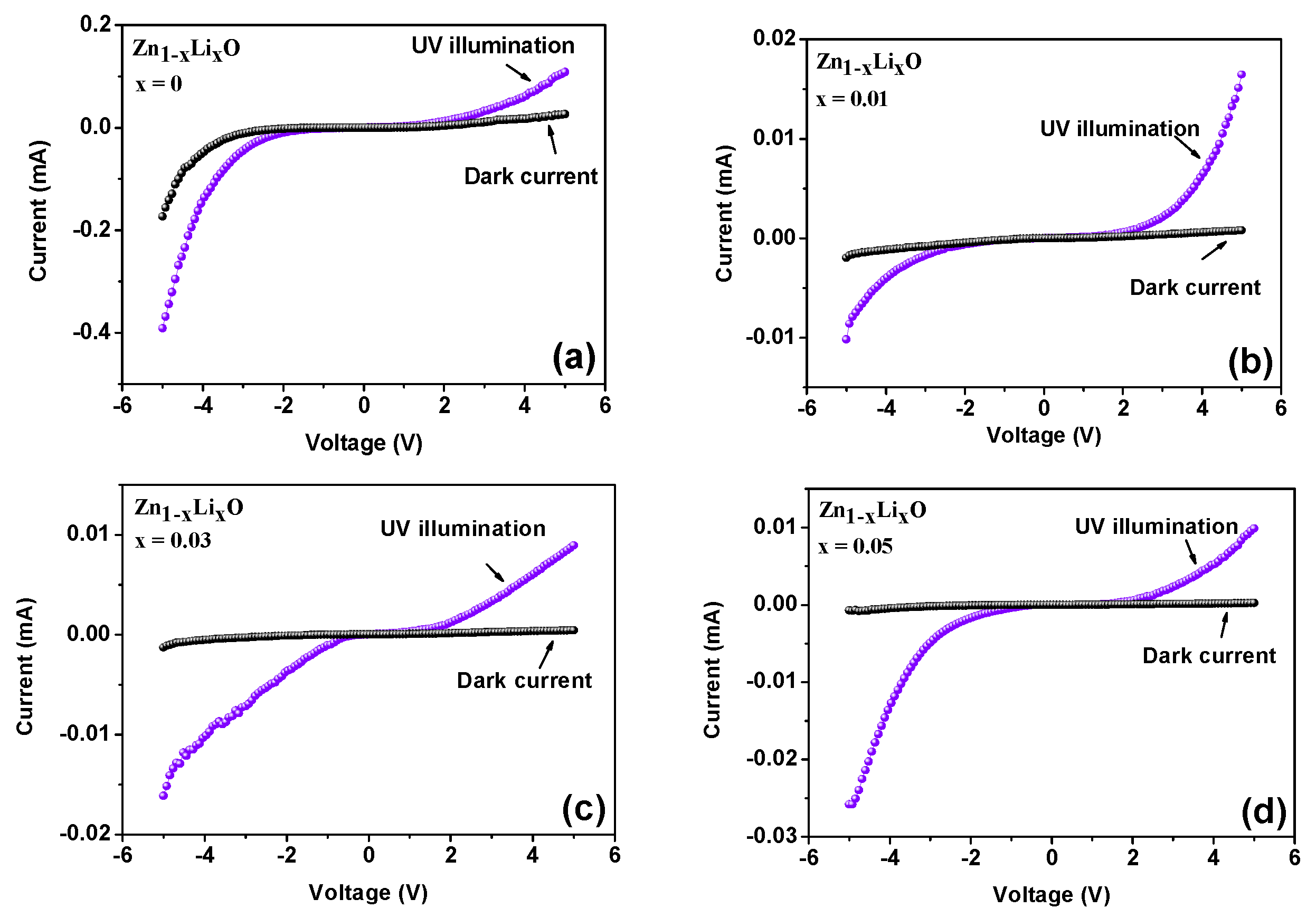
Figure 1. XRD patterns of Zn1−xLixO nanocrystalline films. The inset shows that FWHM broadens with various Li content.
Crystals 08 00228 g001
Figure 2. FE-SEM surface morphology (ad) and cross sectional view images (eh) of Zn1−xLixO nanocrystalline films with x = 0 to 0.05. The average grain size is determined to be 88.02 to 71.16 nm for x = 0 to 0.05.
Crystals 08 00228 g002
Figure 3. PL spectra of Zn1−xLixO nanocrystalline films with x = 0 to 0.05.
Crystals 08 00228 g003
Figure 4. I–V characteristics of Zn1−xLixO nanocrystalline films [(a) x = 0, (b) x= 0.01, (c) x=0.03, (d) x= 0.05] measured under dark and photo-illumination in the voltage from −5 V to +5 V.
Crystals 08 00228 g004
Table 1. Values of Iphoto, Idark, and (Iphoto − Idark)/Idark at +5 V of Zn1−xLixO nanocrystalline films.
Zn1−xLixO (x)Iphoto (mA)Idark (μA)(Iphoto − Idark)/Idark (%)
00.108426.12315
0.010.01640.791975
0.030.00890.412071
0.050.00980.234161

