Large-Scale Assembly and Mask-Free Fabrication of Graphene Transistors via Optically Induced Electrodeposition

1
Department of Computer Science and Technology, Changchun Normal University, Changchun 130032, China
2
State Key Laboratory of Robotics, Shenyang Institute of Automation Chinese Academy of Sciences, Shenyang 110016, China
3
School of Mechatronics Engineering and Automation, Shanghai University, Shanghai 200444, China
*
Authors to whom correspondence should be addressed.
Crystals 2018, 8(6), 239; https://doi.org/10.3390/cryst8060239
Submission received: 19 May 2018
/
Revised: 31 May 2018
/
Accepted: 5 June 2018
/
Published: 7 June 2018
(This article belongs to the Special Issue Graphene Mechanics)
Abstract
:Graphene, known as an alternative for silicon, has significant potential in microelectronic applications. The assembly of graphene on well-defined metal electrodes is a critical step in the fabrication of microelectronic devices. Herein, we present a convenient, rapid, and large-scale assembly method for deposition of Ag electrodes, namely optically induced electrodeposition (OIED). This technique enables us to achieve custom-designed and mask-free fabrication of graphene transistors. The entire assembly process can be completed within a few tens of seconds. Our results show that graphene-based transistors fabricated with Ag electrodes function as a p-type semiconductor. Transfer curves of different samples reveal similar trends of slightly p-type characteristics, which shows that this method is reliable and repeatable.
1. Introduction
Graphene transistors show extraordinary performance because of the unique electronic, physical, and mechanical properties of graphene [1,2,3,4]. To date, the common methods used to assemble and fabricate graphene transistors are e-beam lithography induced deposition [5,6], chemical self-assembly [7] and dielectrophoresis (DEP) [8,9,10,11,12]. Although e-beam lithography induced deposition is compatible with existing micro-fabrication processes, this expensive and complicated manufacturing process is not suitable for low-cost large-scale assembly of graphene. The chemical self-assembly method uses electrostatic interactions to self-assemble graphene sheets onto patterned electrodes via a low-efficiency and uncontrollable process. However, only 10% to 20% of graphene is connected to the electrodes. Owing to its convenient and flexible operating characteristics, many micro/nano-scale materials, such as nanoparticles [13], carbon nanotubes [14], DNA [15] and cells [16], have been assembled onto patterned electrodes via the DEP technique. This method can achieve 100% assembly of graphene; but, the layers of graphene, the position and the direction between graphene and electrodes, and the photomask-induced patterned electrodes are limited to achieve a low-cost, controllable and large-scale graphene device assembly. Optically induced electrodedeposition (OIED), developed from the conventional DEP method, has become a viable technology for assembling micro/nanodevices [17,18]. Utilizing this method, arbitrary configurations of metal electrodes can be directly produced on a computer avoiding conventional mask fabrication. Furthermore, the relative position of graphene and electrodes can be precisely controlled.
This work reports large-scale graphene device assembly via OIED. Chemical vapor deposition (CVD) grown graphene was transferred onto a a-Si:H-based substrate. Because of a poor contrast of graphene on the substrate, “development” electrode arrays were rapidly constructed (within 1 s) to distinguish the position of graphene. Subsequently, Ag electrodes with customized configurations were grown on graphene within 30 s via OIED. The current and voltage measurements were conducted at room temperature under ambient conditions. We observed that graphene-based transistors (FETs) with Ag electrodes exhibit p-type characteristics. The transfer curves of three graphene-based FETs showed that the Dirac points slightly shift to Vg = 0.1, 0.05 and 0.25 V.
2. Materials and Methods
2.1. Materials
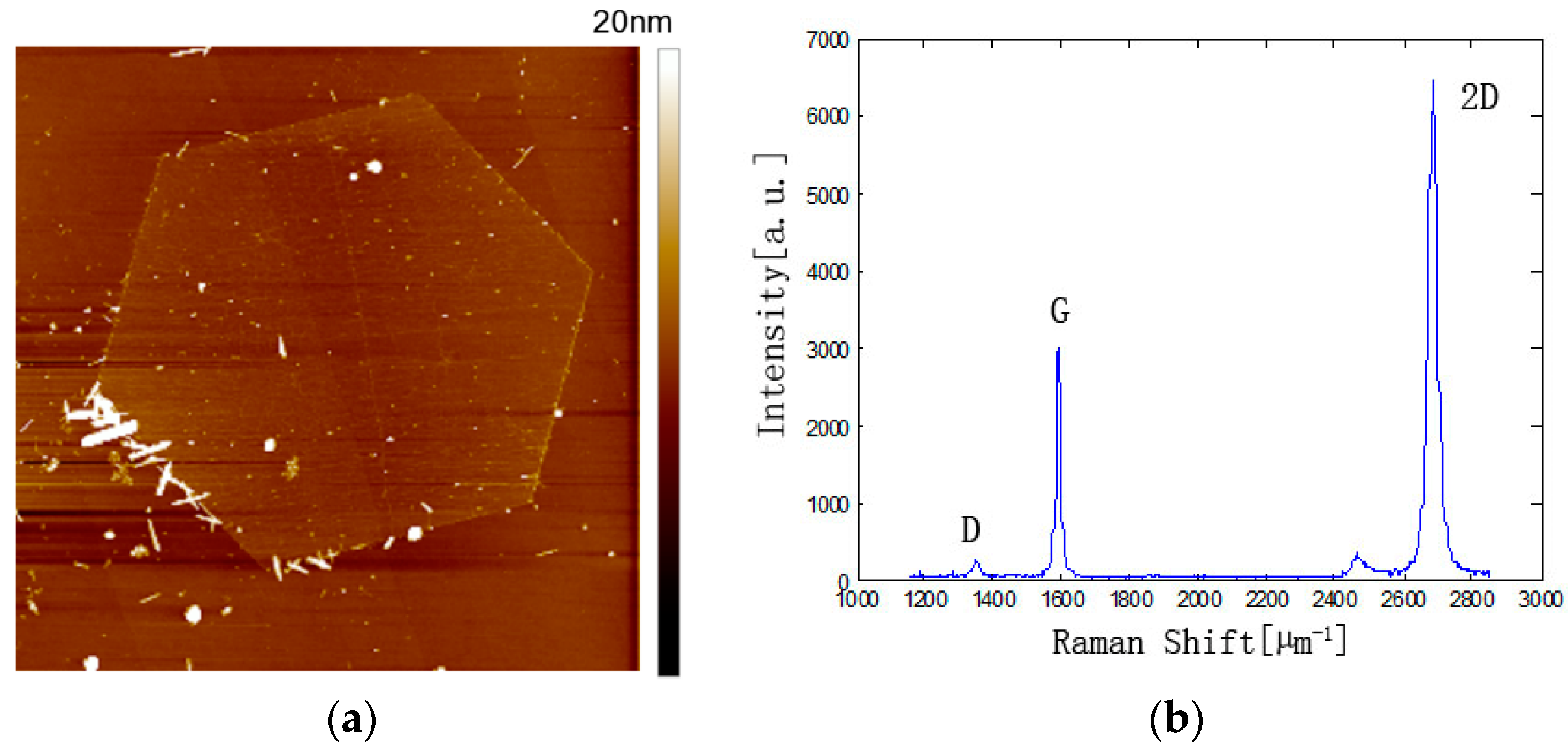
Graphene was prepared by the Institute of Metal Research (IMR), Chinese Academy of Sciences using CVD growth method, as depicted in Reference [19]. A solution with a concentration of 100 mM of ions was prepared by dissolving silver nitrate (≥99.8% purity) in deionized water. This solution provides the raw materials for both determination of the position graphene and fabrication of the Ag electrodes. Graphene was characterized by atomic force microscopy (AFM) in the tapping mode, and the AFM images is shown in Figure 1a. To confirm the number and quality of the graphene, the Raman spectra has been performed, as shown in Figure 1b. The intensity ratio of the 2D and G peak is above 2, which shows the typical features of monolayer graphene. The intensity of D peak, which is associated with disordered carbon atoms and defects, is nearly invisible, indicating the high quality of the graphene.
2.2. Apparatus
The home-made OIED experimental system for fabricating electrodes via the introduction of microfluidic control technology into a conventional optically induced DEP (ODEP) experimental system is shown in Figure 2. The system consists of five functional modules, including a virtual electrode generation module (Flash 11, Adobe, CA, USA), OIED chip (discussed later), projection module (LCD projector, Sony VPL-F400X, Tokyo, Japan; condenser objective, Nikon 50X/0.55, Tokyo, Japan), operation control module (3D Mobile Platform; signal generator, Agilent 33522A, CA, USA), and real-time visual feedback module (CCD, Zoom 160, OPTEM, Alberta, Canada).
2.3. Methods
An Ag electrode was constructed on graphene by oxidation-reduction reaction process:
According to the above reaction, operation will stop, because water in the solution will decompose and eventually dry out during the operating process. In traditional ODEP chips, the solution needs to be injected manually through the inlet (Inlet) with a micro-shifter, as shown in Figure 3a. This issue can be overcome using the OIED system. An OIED chip consists mainly of three components: a photoconductive lower electrode, microfluidic chamber for containing and transporting the electrolyte, and a patterned indium tin oxide (ITO) upper electrode, as shown in Figure 3b. The photoconductive lower electrode substrate consists of predeposited 120 nm-thick ITO and 1 μm-thick a-Si:H fabricated through plasma-enhanced CVD. The upper electrode is a patterned ITO glass. Figure 3c,d show the structure of the patterned ITO glass. First, the inlet, inlet channel, operating area, outlet channel, and outlet have been carved on a double-sided adhesive tape, as shown in Figure 3c. The carved double-sided adhesive tape was then transferred onto an ITO glass, and the inlet and the outlet were drilled for inserting pipes as shown in Figure 3d.
Before electrode deposition, graphene was transferred onto a photoconductive lower electrode by the bubbling transfer method [21]. Pipes were inserted into the inlet and the outlet after the patterned ITO upper electrode and the photoconductive electrode coating with graphene were packaged. A signal generator (Agilent 33522A) that generated a sinusoidal voltage was applied between the top and the bottom ITO electrodes. The flow velocity of the solution in the chamber was controlled by a micro pump (HARVARD PHD 2000). The deposition of the Ag electrode was carried out at an amplitude of 20 Vpp (peak-to-peak voltage) and a frequency of 50 kHz.
After the deposition process, the samples were characterized using a digital microscope (KH-7700 Hirox, Japan), AFM (D3100, Veeco, NY, US), and scanning electron microscope (SEM; Zeiss EVO MA, Oberkochen, Germany). The conductivity of the electrodes and graphene was measured using two tungsten probes with diameters of 5 µm on an analytical probe station. A semiconductor analyzer (Agilent, 4155C) was used to measure the electrical properties at room temperature under ambient conditions.
3. Results and Discussion
3.1. Growth of Ag Electrodes by OIED
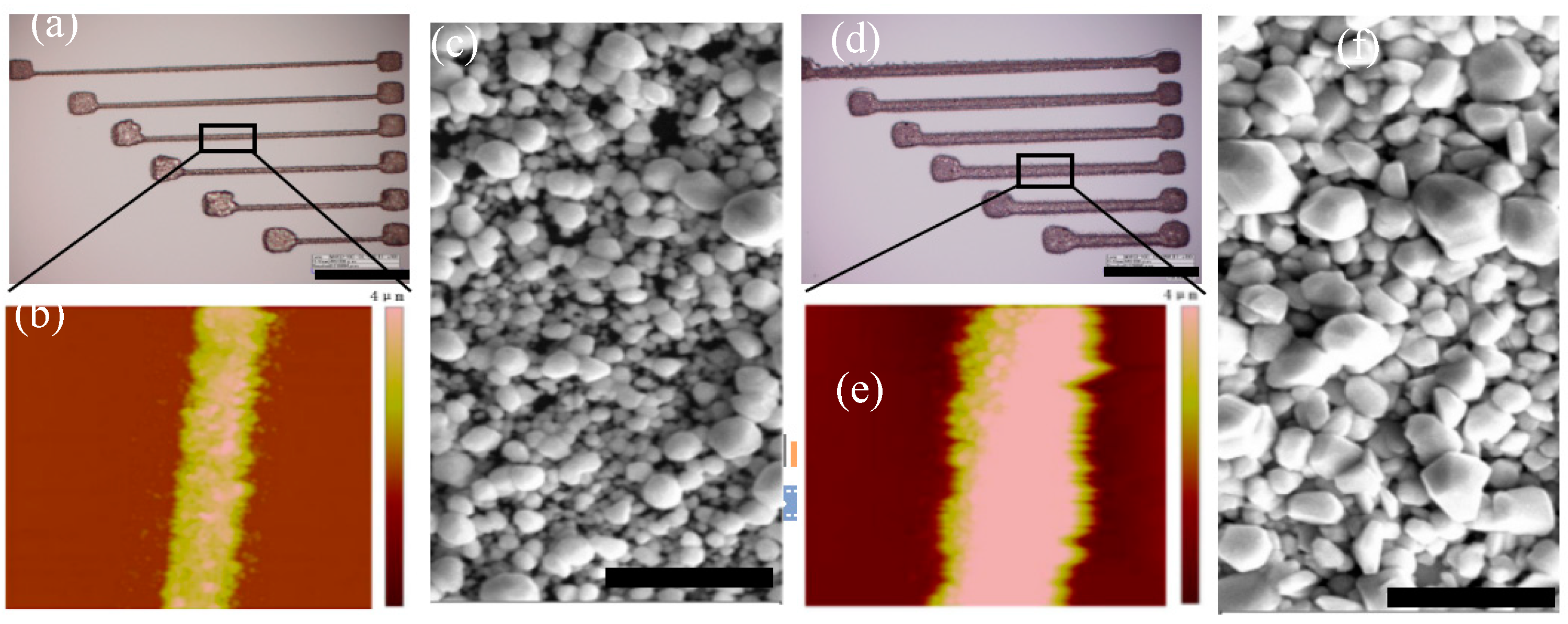
Figure 4 shows the topographic images of Ag electrodes deposited at different time intervals. Figure 4a–f are the characterization results after 10 and 20 s deposition, respectively obtained by optical microscopy, AFM and SEM. The scale bars are 100, 30 and 3 μm, respectively for optical, AFM, and SEM images. The AFM images reveal that the thickness of the Ag electrodes increases with increase in the deposition time. The SEM images show that Ag particles become larger and denser with increase in the deposition time, as shown in Figure 4c,f.
3.2. Large-Scale Assembly of Graphene by OIED
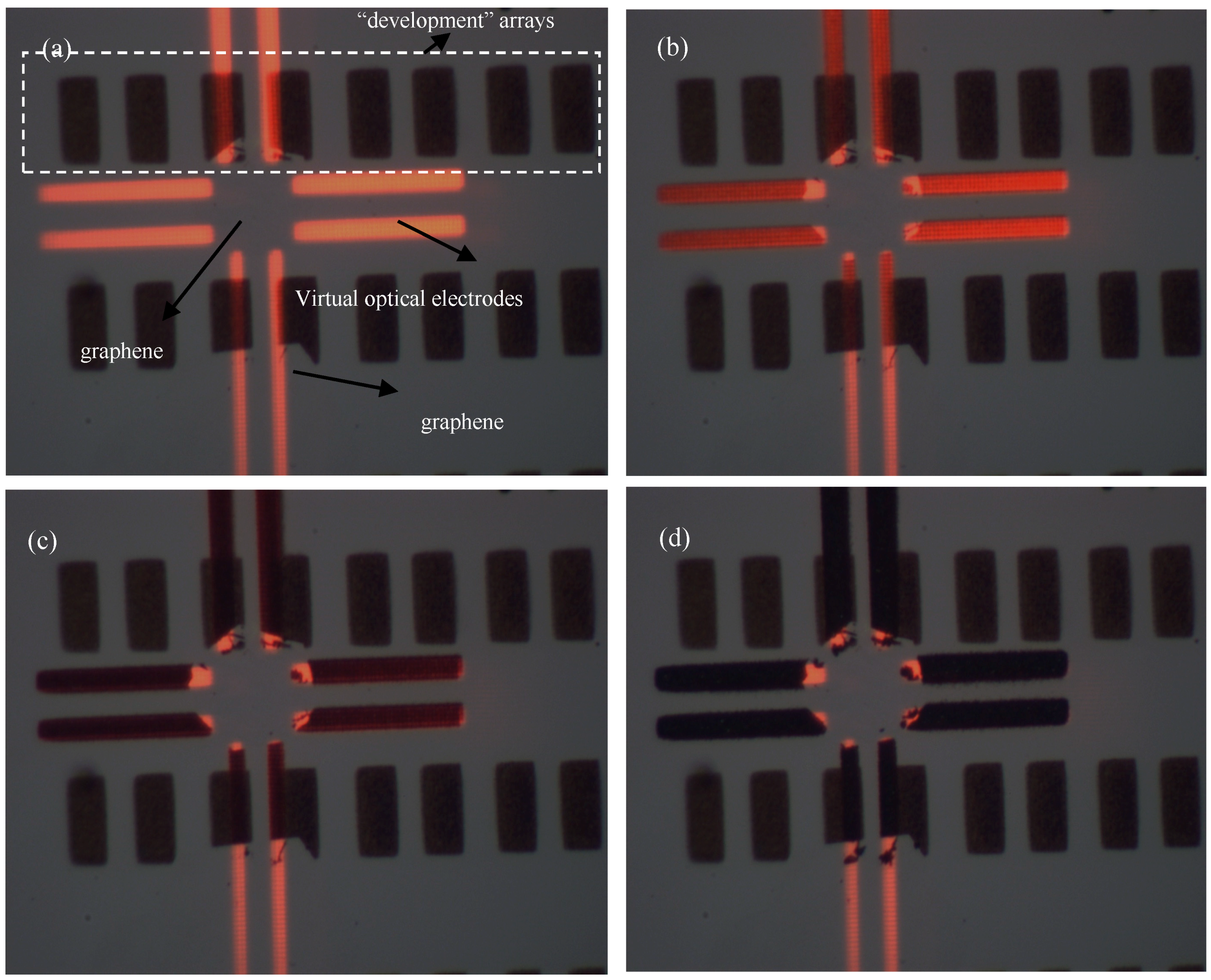
Graphene on an OIED chip cannot be directly observed through a digital microscope; therefore, the position of graphene on the OIED chip needs to be determined before the deposition of the electrodes. Owing to the hydrophobic property of graphene, the electrochemical reaction of the solution on graphene is much slower than that on the a-Si:H substrate. Therefore, the position of graphene can be distinguished by rapidly depositing electrode arrays. These arrays are called “development” arrays; they allow graphene to appear on the substrate like in a photographic film development process. The deposition time of the “development” arrays is very short, usually within 1 s; hence, these electrode arrays are not electrically connected. Figure 5 shows the Ag electrodes deposition process on graphene using the OIED system. The “development” results of graphene on the a-Si:H substrate are as shown in Figure 5a. The white dotted lines indicate the “development” electrode arrays. The edges of graphene are visible in these electrode arrays. After the position of graphene is identified, the patterns of electrodes are dynamically constructed on the computer based on the shape and the position of graphene. The projected patterns are visible as red lighted areas. As shown in Figure 5b–d, the thickness of the deposited Ag electrodes increases with an increase in the deposition time. The deposition time was approximately 30 s.
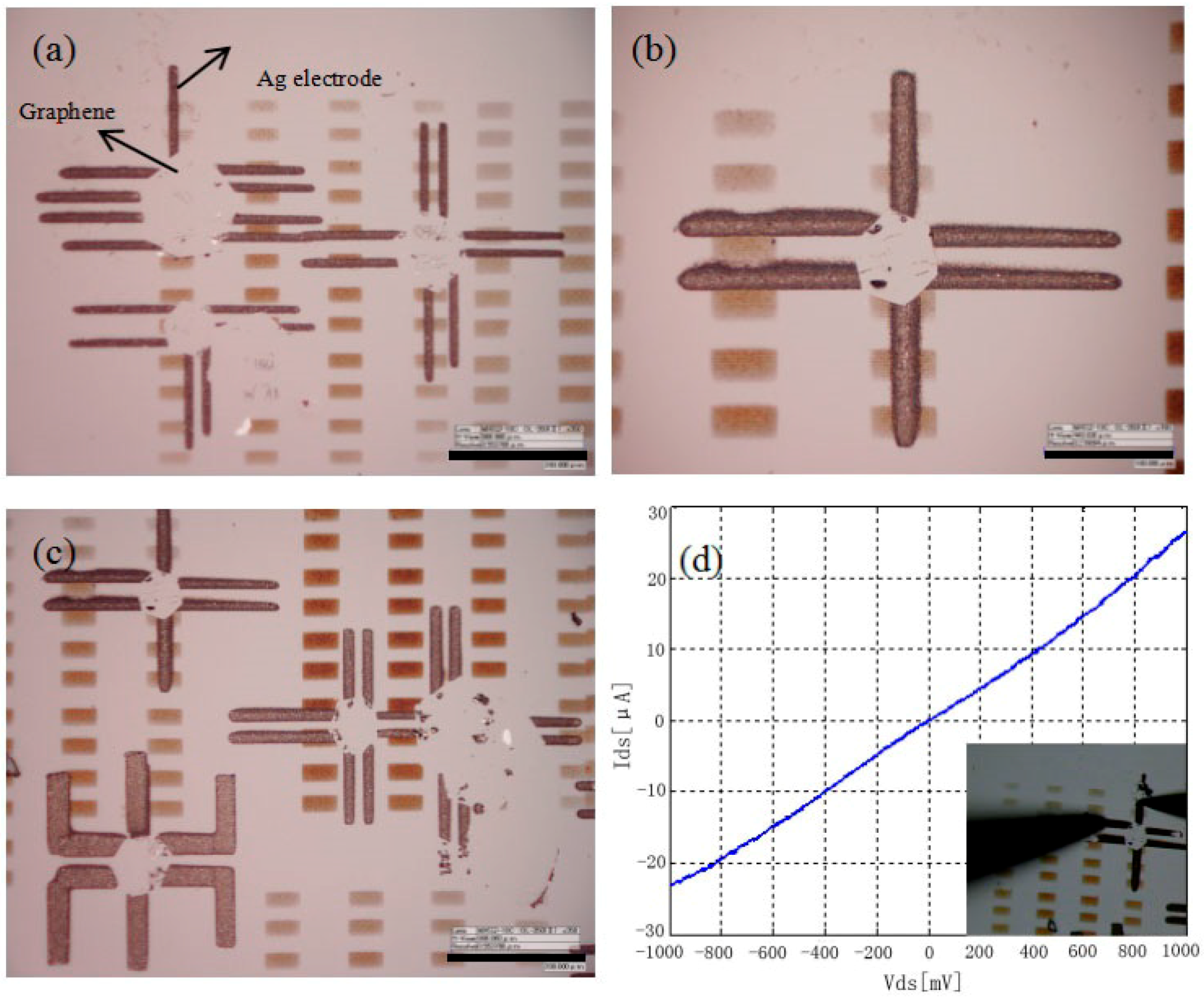
Figure 6a–c show the optical images of large-scale graphene device assembly; the black bars represent 200, 100, and 200 μm, respectively. Different shapes and sizes of Ag electrodes were deposited at the hexagonal edge of graphene with width in the range of 15–30 μm, and Ag deposition occurs at the ripples and defects in graphene. Figure 6d shows the current-voltage characteristics measured using a semiconductor parameter analyzer. The Ag electrode is electrically connected to graphene though an Ohmic connection. The inset in Figure 6d is the optical image of two tungsten probes connecting the electrodes on an analytical probe station for the measurement of current-voltage characteristics.
3.3. The Structure and Electrical Characteristics of Assembled Graphene-Based FETs
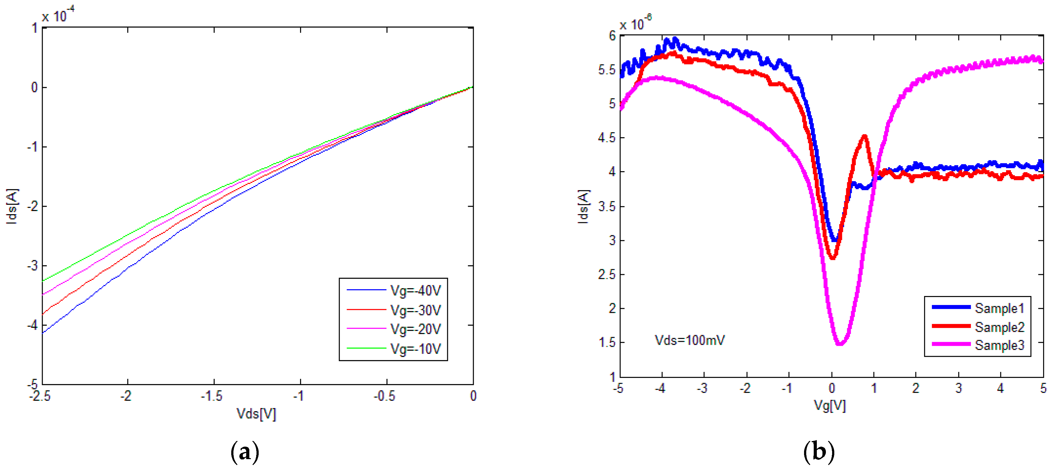
The electrical characteristics of the assembled graphene-based FETs with Ag electrodes were measured at room temperature under ambient conditions using a semiconductor parameter analyzer (Agilent 4155C). As shown in Figure 7a, the output curves were measured with a fixed gate voltage (Vg) from −40 to −10 V in steps of −10 V. The output curves indicate that the graphene-based FET exhibits p-type characteristics. The main charge carriers are holes, and as the concentration of the holes increase when the Vg is negative, the graphene resistance decreases. The transfer curves were measured at a fixed drain voltage of 100 mV for three samples, as shown in Figure 7b. The Dirac points are at Vg = 0.1, 0.05, and 0.25. The G and 2D bands upshift to ~1590 and ~2685 cm−1, which shows typical features of p-doping. The slight shift in the Dirac point reveals that this method is reliable and repeatable.
4. Conclusions
In summary, a large-scale assembly of graphene has been successfully realized using OIED. Both the electrode shapes and sizes could be dynamically controlled in real-time without using any conventional lithography procedures during the entire assembly process. Silver electrodes could be fabricated rapidly within a few tens of seconds and were electrically connected to graphene though an Ohmic connection. Furthermore, current and voltage measurements of the graphene-based FETs with Ag electrodes show p-type characteristics. The Dirac points are slightly shifted to Vg = 0.1, 0.05, and 0.25 V, respectively. Our future work will investigate the contact resistance of devices with different metal contacts and deposition intervals. Unlike the conventional technique, the presented method could achieve a bottom-up, high-efficiency and low-cost assembly of graphene at precise locations, demonstrating the potential as a robust and highly efficient method for the fabrication of nanoelectronic devices using other emerging two-dimensional materials.
Author Contributions
Y.Z. designed and performed experiments and measurements, carried on data analysis and drafted the manuscript. N.L. and Y.Z. performed Ag electrode deposition and discussed the results. Y.Y., F.Y., H.Y. and N.J. participated in the monitoring the experimental work and revision of the manuscript.
Acknowledgments
This work supported by National Natural Science Foundation of China (Grant No. 61604019, 61703265), Natural Science Foundation of Jilin Province, China (Grant No. 20160520098JH), and Talent introduction scientific research project of Changchun Normal University, China (RC2016009).
Conflicts of Interest
The authors declare no conflicts of interest.
References
- Novoselov, K.S.; Falko, V.I.; Colombo, L.; Gellert, P.R.; Schwab, M.G.; Kim, K. A roadmap for graphene. Nature 2012, 490, 192–200. [Google Scholar] [CrossRef] [PubMed]
- Zhang, Y.; Yu, F.H.; Li, G.Y.; Liu, L.Q.; Liu, G.J.; Zhang, Z.Y.; Wang, Y.C.; Weijnya, U.C.; Xi, N. Online Determination of Graphene Lattice Orientation Through Lateral Forces. Nanoscale Res. Lett. 2016, 11, 353. [Google Scholar] [CrossRef] [PubMed]
- Wang, Y.; Yang, T.; Lao, J.; Zhang, R.; Zhang, Y.; Zhu, M. Ultra-sensitive graphene strain sensor for sound signal acquisition and recognition. Nano Res. 2015, 8, 1627–1636. [Google Scholar] [CrossRef]
- Ghadiry, M.; Ismail, R.; Saeidmanesh, M.; Khaledian, M.; Manaf, A. Graphene nanoribbon field-effect transistor at high bias. Nanoscale Res. Lett. 2014, 9, 604. [Google Scholar] [CrossRef] [PubMed] [Green Version]
- Lemme, M.C.; Bell, D.C.; Williams, J.R. Etching of Graphene Devices with a Helium Ion Beam. ACS Nano 2009, 3, 2674–2676. [Google Scholar] [CrossRef] [PubMed] [Green Version]
- Yang, W.; Berthou, S.; Lu, X.; Wilmart, Q.; Denis, A.; Rosticher, M.; Taniguchi, T.; Watanabe, K.; Fève, G.; Berroir, J.; et al. A graphene Zener–Klein transistor cooled by a hyperbolic substrate. Nat. Nanotechnol. 2018, 13, 47–52. [Google Scholar] [CrossRef] [PubMed]
- Wang, H.; Wang, X.; Li, X.; Dai, H. Chemical self-assembly of graphene sheets. Nano Res. 2009, 2, 336–342. [Google Scholar] [CrossRef] [Green Version]
- Kang, H.; Kulkarni, A.; Stankovich, S.; Ruoff, R.S.; Baik, S. Restoring electrical conductivity of dielectrophoretically assembled graphite oxide sheets by thermal and chemical reduction techniques. Carbon 2009, 47, 1520–1525. [Google Scholar] [CrossRef]
- Burg, B.R.; Lutolf, F.; Schneider, J.; Schirmer, N.C.; Schwamb, T.; Poulikakos, D. High-yield dielectrophoretic assembly of two-dimensional graphene nanostructures. Appl. Phys. Lett. 2009, 94, 053110. [Google Scholar] [CrossRef]
- Joung, D.; Chunder, A.; Zhai, L.; Khondaker, S.I. High Yield Fabrication of Chemically Reduced Graphene Oxide Field Effect Transistors by Dielectrophoresis. Nanotechnology 2010, 21, 165202. [Google Scholar] [CrossRef] [PubMed]
- Burg, B.R.; Schneider, J.; Maurer, S.; Schimer, N.C.; Poulikakos, D. Dielectrophoretic integration of single and few layer graphenes. J. Appl. Phys. 2010, 107, 034302. [Google Scholar] [CrossRef]
- Zhang, Y.; Liu, L.; Xi, N.; Wang, Y.; Dong, Z.; Wejinya, U.C. Dielectrophoretic Assembly and AFM Modification of Reduced Graphene Oxide. J. Appl. Phys. 2011, 110, 114545. [Google Scholar] [CrossRef]
- Leiterer, C.; Deckert-Gaudig, T.; Singh, P.; Wirth, J.; Deckert, V.; Fritzsche, W. Dielectrophoretic positioning of single oparticles on atomnanic force microscope tips for tip-enhanced Raman spectroscopy. Electrophoresis 2015, 36, 1142–1148. [Google Scholar] [CrossRef] [PubMed]
- Shekhar, S.; Stokes, P.; Khondaker, S. Ultrahigh density alignment of carbon nanotube arrays by dielectrophoresis. ACS Nano 2011, 5, 1739–1746. [Google Scholar] [CrossRef] [PubMed]
- Viefhues, M.; Eichhorn, R. DNA dielectrophoresis theory and applications a review. Eelectrophoresis 2017, 38, 1483–1506. [Google Scholar] [CrossRef] [PubMed]
- Song, H.; Rosano, J.M.; Wang, Y.; Garson, C.J.; Prabhakarpandian, B.; Pant, K.; Klarmann, G.J.; Perantoni, A.; Alvarez, L.M.; Lai, E. Continuous-flow sorting of stem cells and differentiation products based on dielectrophoresis. Lab Chip 2015, 15, 1320–1328. [Google Scholar] [CrossRef] [PubMed]
- Liu, N.; Wei, F.N.; Liu, L.Q.; Lai, H.S.S.; Yu, H.B.; Wang, Y.C.; Lee, G.; Li, W.J. Optically-controlled digital electrodeposition of thin-film metals for fabrication of nano-devices. Opt. Mater. Express 2015, 5, 838–848. [Google Scholar] [CrossRef]
- Liu, N.; Wang, F.F.; Liu, L.Q.; Yu, H.B.; Xie, S.; Wang, J.; Wang, Y.C.; Lee, G.; Li, W.J. Rapidly patterning micro/nano devices by directly assembling ions and nanomaterials. Sci. Rep. 2016, 6, 32106. [Google Scholar] [CrossRef] [PubMed] [Green Version]
- Ma, T.; Ren, W.C.; Liu, Z.B.; Huang, L.; Ma, L.P.; Ma, X.L.; Zhang, Z.Y.; Peng, L.M.; Cheng, H.M. Repeated Growth-Etching-Regrowth for Large-Area Defect-Free Single-Crystal Graphene by Chemical Vapor Deposition. ACS Nano 2014, 8, 12806–12813. [Google Scholar] [CrossRef] [PubMed]
- Wang, S. Theoretical Analysis and Experimental Method of Optically Induced Dielectrophoresis for Micro/Nano Manipulation; Shenyang Institute of Automation, Chinese Academy of Sciences: Shenyang, China, 2011. [Google Scholar]
- Gao, L.B.; Ren, W.C.; Xu, H.L.; Jin, L.; Wang, Z.; Ma, T.; Ma, L.P.; Zhang, Z.; Fu, Q.; Peng, L.M.; et al. Repeated Growth and Bubbling Transfer of Graphene with Millimetre-size Single-crystal Grains Using Platinum. Nat. Commun. 2012, 3, 699. [Google Scholar] [CrossRef] [PubMed]
Figure 1.
(a) Height image of the graphene in AFM tapping mode. Scan size: 30.0 µm × 30.0 µm; (b) Raman spectroscopy measurement of the intensity of the D and G peaks on the graphene layer in (a). The D, G and 2D Raman peaks for the graphene are labeled.
Figure 1.
(a) Height image of the graphene in AFM tapping mode. Scan size: 30.0 µm × 30.0 µm; (b) Raman spectroscopy measurement of the intensity of the D and G peaks on the graphene layer in (a). The D, G and 2D Raman peaks for the graphene are labeled.

Figure 2.
(a) Experimental setup of optically induced electrodeposition (OIED); (b) the OIED chip where electrochemical reactions occur.
Figure 2.
(a) Experimental setup of optically induced electrodeposition (OIED); (b) the OIED chip where electrochemical reactions occur.
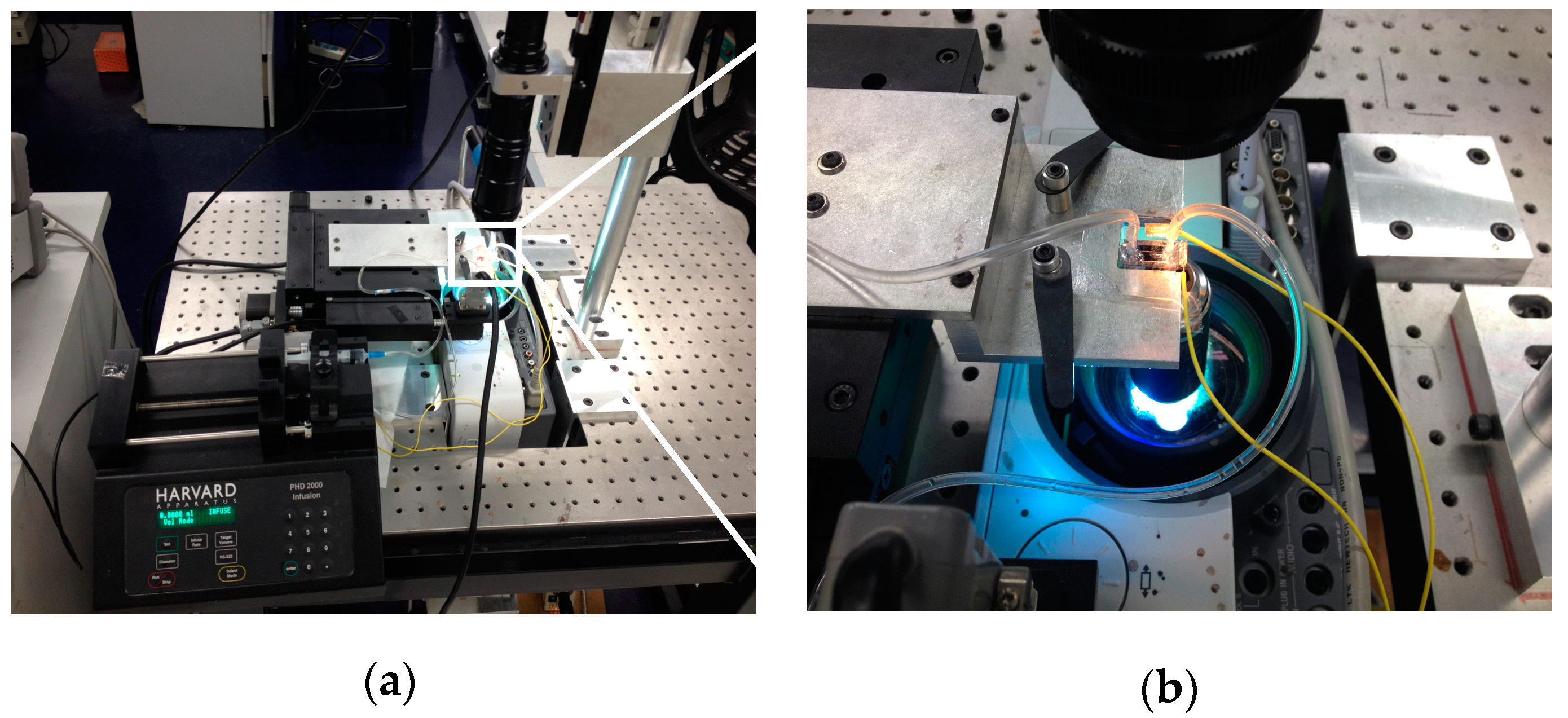
Figure 3.
(a) Conventional ODEP chip [20]; (b) schematic illustration of the structure of the OIED chip; (c) pattern to be fabricated on double-sided adhesive tape; (d) patterned ITO glass.
Figure 3.
(a) Conventional ODEP chip [20]; (b) schematic illustration of the structure of the OIED chip; (c) pattern to be fabricated on double-sided adhesive tape; (d) patterned ITO glass.
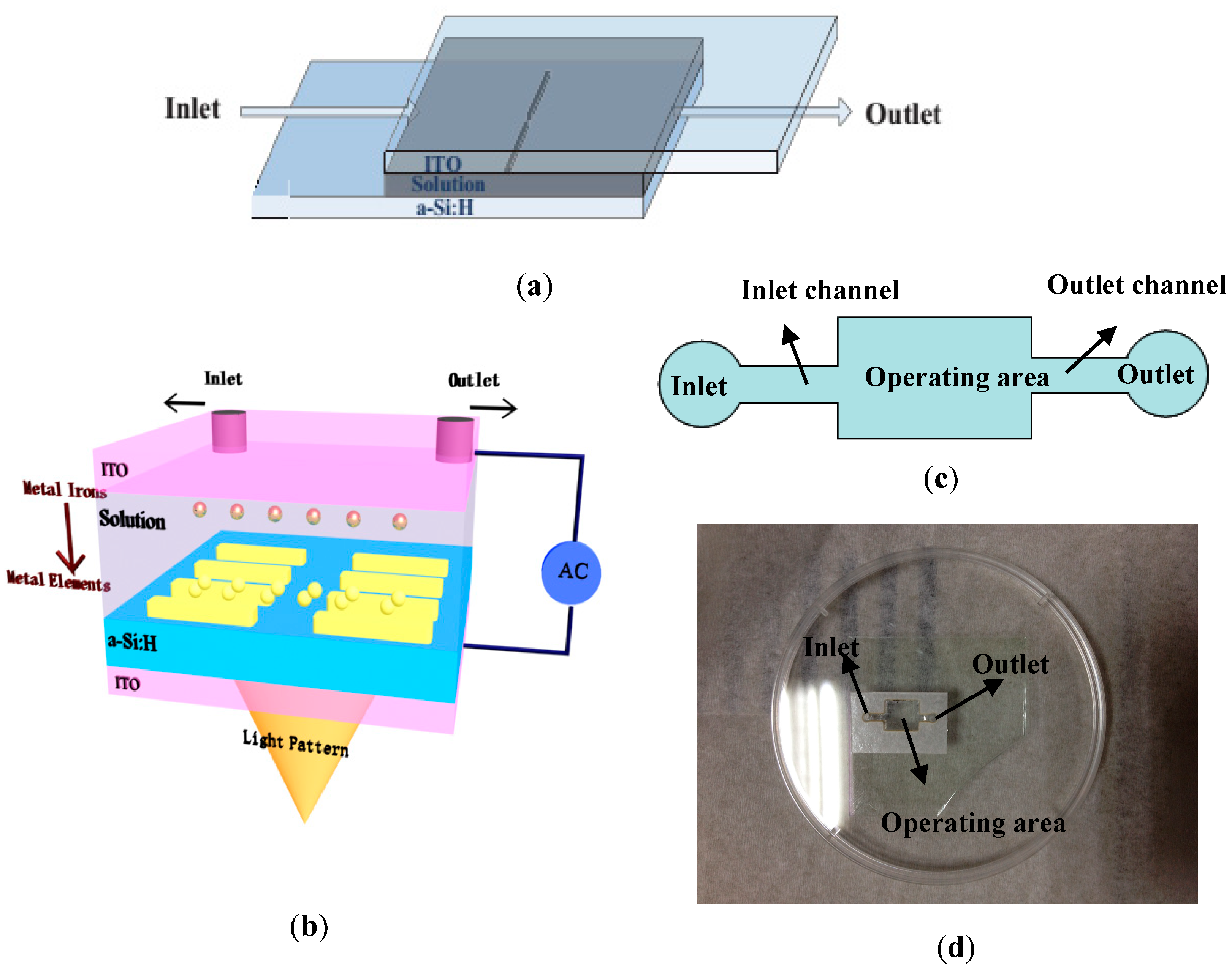
Figure 4.
Optical, AFM, and SEM images of the Ag electrodes deposited at different time intervals. (a,d) Optical images of Ag electrodes deposited with in 10 and 20 s, respectively. Both the bars represent 100 μm; (b,e) magnified AFM images of the black square-enclosed regions in panels a and d, respectively. Both the scale bars represent 4 μm. Scan size: 30 μm × 30 μm; (c,f) topographic images of the surfaces of the Ag electrodes obtained via SEM. Both the bars represent 3 μm.

Figure 5.
Optical images of the Ag electrodes deposition process using the OIED system. (a) Images of graphene appearing on the substrate though “development” arrays indicated by white dotted lines. The red rectangles are virtual optical electrodes designed by using a commercial personal computer software (Flash 11, Adobe); (b–d) Ag electrode deposition process. The shape of graphene becomes visible and the thickness of the electrodes increases during the process.

Figure 6.
Large-scale graphene device assembly and current-voltage characteristics. (a–c) Optical images of different configurations of Ag electrodes connected at the edges of graphene. The hexagonal shapes correspond to single-crystal graphene. The black bars are 200, 100, and 200 μm, respectively in (a–c); (d) current–voltage characteristics. The inset shows the optical image of two tungsten probes connecting the electrodes on an analytical probe station.

Figure 7.
Electrical characteristics of the graphene-based FETs. (a) Output curves of the graphene-based FET for Vds = 0–2.5 V, with Vg ranging from −40 to −10 V; (b) transfer curves of the graphene-based FETs at Vg = −5–5 V and a fixed Vds of 100 mV.
Figure 7.
Electrical characteristics of the graphene-based FETs. (a) Output curves of the graphene-based FET for Vds = 0–2.5 V, with Vg ranging from −40 to −10 V; (b) transfer curves of the graphene-based FETs at Vg = −5–5 V and a fixed Vds of 100 mV.
© 2018 by the authors. Licensee MDPI, Basel, Switzerland. This article is an open access article distributed under the terms and conditions of the Creative Commons Attribution (CC BY) license (http://creativecommons.org/licenses/by/4.0/).
Share and Cite
MDPI and ACS Style
Zhang, Y.; Yang, Y.; Liu, N.; Yu, F.; Yu, H.; Jiao, N. Large-Scale Assembly and Mask-Free Fabrication of Graphene Transistors via Optically Induced Electrodeposition. Crystals 2018, 8, 239. https://doi.org/10.3390/cryst8060239
AMA Style
Zhang Y, Yang Y, Liu N, Yu F, Yu H, Jiao N. Large-Scale Assembly and Mask-Free Fabrication of Graphene Transistors via Optically Induced Electrodeposition. Crystals. 2018; 8(6):239. https://doi.org/10.3390/cryst8060239
Chicago/Turabian StyleZhang, Yu, Yong Yang, Na Liu, Fanhua Yu, Haibo Yu, and Niandong Jiao. 2018. "Large-Scale Assembly and Mask-Free Fabrication of Graphene Transistors via Optically Induced Electrodeposition" Crystals 8, no. 6: 239. https://doi.org/10.3390/cryst8060239
Note that from the first issue of 2016, this journal uses article numbers instead of page numbers. See further details here.