Review

Influence of Dislocations in Transition Metal Oxides on Selected Physical and Chemical Properties

1
Peter Grünberg Institute (PGI-7) Forschungszentrum Jülich, 52425 Jülich, Germany
2
JARA-FIT, Forschungszentrum Jülich, 52425 Jülich, Germany
3
Institute of Physics, University of Silesia, 40-007 Katowice, Poland
4
Peter Grünberg Institute (PGI-1) Forschungszentrum Jülich, 52425 Jülich, Germany
5
Institute of Engineering Innovation, School of Engineering, The University of Tokyo, Tokyo 113-8656, Japan
*
Author to whom correspondence should be addressed.
Crystals 2018, 8(6), 241; https://doi.org/10.3390/cryst8060241
Submission received: 6 March 2018 / Revised: 23 May 2018 / Accepted: 27 May 2018 / Published: 4 June 2018
(This article belongs to the Special Issue Crystal Dislocations: Their Impact on Physical Properties of Crystals)

Abstract

:
Studies on dislocations in prototypic binary and ternary oxides (here TiO2 and SrTiO3) using modern TEM and scanning probe microscopy (SPM) techniques, combined with classical etch pits methods, are reviewed. Our review focuses on the important role of dislocations in the insulator-to-metal transition and for redox processes, which can be preferentially induced along dislocations using chemical and electrical gradients. It is surprising that, independently of the growth techniques, the density of dislocations in the surface layers of both prototypical oxides is high (109/cm2 for epipolished surfaces and up to 1012/cm2 for the rough surface). The TEM and locally-conducting atomic force microscopy (LCAFM) measurements show that the dislocations create a network with the character of a hierarchical tree. The distribution of the dislocations in the plane of the surface is, in principle, inhomogeneous, namely a strong tendency for the bundling and creation of arrays or bands in the crystallographic <100> and <110> directions can be observed. The analysis of the core of dislocations using scanning transmission electron microscopy (STEM) techniques (such as EDX with atomic resolution, electron-energy loss spectroscopy (EELS)) shows unequivocally that the core of dislocations possesses a different crystallographic structure, electronic structure and chemical composition relative to the matrix. Because the Burgers vector of dislocations is per se invariant, the network of dislocations (with additional d1 electrons) causes an electrical short-circuit of the matrix. This behavior is confirmed by LCAFM measurements for the stoichiometric crystals, moreover a similar dominant role of dislocations in channeling of the current after thermal reduction of the crystals or during resistive switching can be observed. In our opinion, the easy transformation of the chemical composition of the surface layers of both model oxides should be associated with the high concentration of extended defects in this region. Another important insight for the analysis of the physical properties in real oxide crystals (matrix + dislocations) comes from the studies of the nucleation of dislocations via in situ STEM indentation, namely that the dislocations can be simply nucleated under mechanical stimulus and can be easily moved at room temperature.

1. Introduction

The challenge of an extensive treatise about the influence of dislocations in oxides on the physical and chemical properties in form of a short review is, without doubt, demanding. For instance, the analysis of the modification of the mechanical properties (especially plasticity) in multinary oxides as an effect of the existence of a high density of dislocations in crystalline or polycrystalline oxides can be found in many articles (see, e.g., [1,2,3,4,5,6,7,8,9,10,11,12,13,14,15,16,17,18,19,20,21,22,23,24,25,26,27,28,29,30,31,32,33,34,35,36,37,38,39,40,41,42,43,44,45,46] and references therein). Similarly, the literature about the role of filaments and their possible relation to dislocations in the resistive switching phenomena in oxides is continuously growing (e.g., [30,31,32,33,47,48,49,50,51,52,53,54,55,56,57,58,59] and their references). Therefore, it is necessary to select a group of oxides and a list of properties which could be presented in such a review, by taking into account the actual state-of-the-art in this subject. In our paper, we will focus on two prototypical oxide materials as representative model systems for the binary and ternary oxides with early transition metals, here TiO2 and SrTiO3. For our study of the physical and chemical properties we will furthermore concentrate the attention on those properties which can only be understood on the basis of a comprehensive knowledge of the electronic, chemical, and crystallographic structure of the core of dislocations as derived from modern microscopic techniques such as high-resolution transmission electron microscopy (HRTEM, with spherical aberration correction), electron-energy loss spectroscopy (EELS), scanning transmission electron microscopy with chemical resolution (ChemiSTEM) studies and scanning probe microscopy (SPM) analysis, such as atomic force microscopy (AFM), Kelvin-probe force microscopy (KPFM), piezo force microscopy (PFM), or locally-conducting AFM (LCAFM). However, that this does not mean that we will neglect the other more classical techniques as, for example, etch pits technique or X-ray topography in our presentation. The microscopic analysis, which has become available during recent years, especially by HRTEM (e.g., [4,5,6,7,8,9,10,11,12,13,29,33,46,60,61,62,63,64,65]) and SPM analysis (e.g., [53,55,66,67,68]), allows for us to underpin our hypothesis that the dislocations in band-insulating transition metal oxides take the role of semi-conducting or metallic nano-wires (e.g., [3,13,32,40,50,51,55,68]). We place special emphasis on this problem, namely that the properties of the local stoichiometry and specifically the valence of the transition metal cations close to the core of dislocations is responsible for the kind of specific electric properties of the dislocations encountered in these materials and that allows for considering the dislocation lines as a kind of nano-wire extending throughout the crystal. In fact, it is the specific electronic structure of the core of dislocations in connection with the invariance of the Burges vector of dislocations which generates a kind of macroscopically relevant “entity” in the real oxide crystals, here the perfect matrix with a network of short-circuit dislocations. We will also show that the dislocations can be electrically addressed and individually modified by external means as well as macroscopically aligned in these materials. A further important topic of our paper is connected with existence of an enhanced concentration of dislocations in the surface layer of TiO2 and SrTiO3 oxides which gives rise to the ability of chemical and physical transformations of the surface layer at high temperature for different oxygen partial pressures ([68] and references therein). Finally, we also briefly discuss the plastic properties of the oxides in presence of dislocations. Of course, it is self-evident that the variety of properties of both model oxides, which can be potentially modified by dislocations, is clearly broader than the mentioned points of our list.

2. Edge Dislocations in TiO2 and SrTiO3

From a topological point of view, edge dislocations, screw dislocations and dislocation loops belong to the class of “1”-dimensional extended defects. In the classical presentation of edge dislocations (see Figure 1) they should be imagined as the end of an extra half plane which is shifted into the perfect matrix [1,21,25,26,27,32,34,37]. The end of the half plane defines, in fact, the position of the dislocation line. This representation can be used without modification for a schematic visualization of the distribution of atoms along the dislocations in TiO2. In contrast to the classical presentation of dislocation lines in TiO2, dislocation lines in case of a ternary oxide, such as SrTiO3, should be represented by the end of two half planes (namely TiO2 and SrO), which have been shifted into the matrix of SrTiO3 (Figure 2) [39,69]. In the other situation with a shift of only one half plane (i.e., TiO2 or SrO), the configuration corresponds to the generation of a stacking fault, and the dislocation in its character will be partial [65,68].
For rutile crystals, which at room temperature possess a tetragonal structure, the orientation of the edge dislocation can be realized in different directions. Because each of the edge dislocations with defined Burgers vector can lie in different planes (so-called slip system) we can observe different combinations between the mentioned crystallographic directions of the dislocations and the plane, e.g., {101}<101>, {110}<001> [70,71], (101){010}, (111){101}, and (100){101} [37].
For the SrTiO3 crystal, which has a cubic structure (Pm3m) above 110 K, it has been observed that the edge dislocations can, in principle, be arranged with Burgers vector in direction <100>, <110>, and <111>. Those directions, in combination with the appropriate plane, give the following possibilities of slip systems for SrTiO3: <100>{110}, <001>{110}, <011>{100}, and <010>{100} [73].
The mentioned set of the dislocation directions does not describe all of the possibilities concerning the crystallographic orientation of dislocation lines and assignment of the slip system. It is possible that in SrTiO3 crystals, dislocations can be generated with higher index, for example [012] [74]. In this case, the dislocation core is more complicated than for dislocations with a low index, that is, the structure should be analyzed as an overlap of many partial dislocations (with lower indexes) and other non-invariant extended defects such as stacking faults (see Figure 3).

3. Arrangement of Dislocations

Dislocations do not only exist as individual objects which extend throughout the crystalline material, but the dislocations in real systems can accumulate in bundles, line arrays, bands as well as in three-dimensional networks [75]. One aspect of the arrangement of dislocations is the dislocation-dislocation interaction and, in the oxide materials considered here, the issue of the electrostatics of dislocations and their surroundings comes into play. In the sense of Kröger–Vink defect chemistry, charged defects should interact with other charged defects because the crystal as a whole has to fulfill the electroneutrality condition demanding that the sum of all charged defects such as electrons, holes, and vacancies has to be zero in steady state [70,76,77,78,79,80,81,82,83,84,85,86,87,88,89]. Because some of the d0 Ti states along the dislocations in TiO2 and SrTiO3 are transformed into d1 configuration, such dislocations with a surplus of d electrons cannot be electrically neutral (e.g., [31]). Hence, a screening of the electrical charge which has accumulated along the core of the dislocations is needed. Therefore, such screening leads to the creation of a space charge zone, the extension of which depends (in the first approximation) on the concentration of the charge (the mentioned concentration of d1 electrons) in the core of the dislocations, the concentration of the charged defects in the matrix and its dielectric properties. [31,32,90,91,92,93,94,95]. This screening, in fact, induces a kind of electrostatic repulsion forces between similarly charged dislocations. Such Coulomb repulsion can hinder a potential accumulation, for instance, a bundling of dislocations. Of course, it is possible that in case of oppositely charged cores of dislocations the interaction can be attractive and an annihilation of dislocations takes place [96,97]. Notice: for the analyses of the relaxed configuration of the dislocations in the matrix (that means with a fixed position) of ionic or ionic covalent oxides one should not only take into account the minimum of the electrostatic energy but also the minimization of the total free energy of the crystal, which in this case means the minimization of the mechanical energy (here the stress). Therefore, when the density of generated and annihilated dislocations does not change (at constant temperature and constant internal or external stress), ρ ˙ + = ρ ˙ (ρ is the density of dislocations with opposite sign), the total density of dislocations is given by:
ρ ( ε ) = ρ 0 + 0 ϵ ( ρ ˙ + ρ ˙ ) ε ˙ 1 d ε
and the deformation rate ε ˙ should be constant. This classical description for the generation of the edge dislocations in metal or single oxides (binary oxides) cannot be one-to-one transferred on the situation in SrTiO3, where the dislocations can possess a different chemical core (see e.g., [39]) which per se induces different local stress fields, and the interaction of edge dislocations with the same Burgers vector, cannot be simply interpreted [98].
Despite this electrostatic “inadequacy”, one can clearly see, based on empirical findings by different techniques, that the edge dislocations in case of SrTiO3 and TiO2 are often found to be accumulated in bundles, line arrays, bands and in three dimensional networks of dislocations (see, e.g., [10,42,99,100,101,102,103,104]). All processes which can lead to new arrangements of dislocations in the matrix are connected with two basic possibilities to move the dislocations in the matrix. The first one is a conservative moving (gliding) of dislocations, which occurs when, by a change of the position of the dislocations in the crystalline structure, its Burgers vector and the dislocations line belong to the same plane. The other possibility for the moving of dislocations (so-called non-conservative motion or climbing) occurs when the mentioned condition for gliding is not fulfilled. This standard description of the conservative and non-conservative motion of dislocations is, in fact, valid for metals and nonmetals, but for ionic oxides there is an additional “hidden dimension” of the motion, especially for climbing, namely a complicated non-synchronous evolution (on the time scale) of the positions of ions or charged vacancies (see Figure 4). Because the diffusion of oxygen vacancies is easier than that of cation vacancies, this process cannot be realized in only one step. The detailed scenario of all steps of the climbing of the dislocations in this electrical complicated surrounding has been described by Hirel et al. [105].
The motion of dislocations in oxide crystals cannot only be analyzed under electrical (electrostatic) aspects, but also gliding or climbing mechanisms should be discussed in terms of strain and temperature. This set of thermodynamic parameters can, for example, radically change the character of the gliding of dislocations in SrTiO3 crystals. At room temperature (RT) easy gliding of dislocations in SrTiO3 allows for dramatic plastic deformation (in fact, the crystal can be bent by bare hands [107]). For this temperature, it should be accepted that the coordinated gliding of dislocations (as an origin of the significant plastic deformation) occurs without a change of the core structure (see Figure 5A). In contrast, at higher temperature the ductility of the crystal is lower and the crystal will become brittle [16,33,108,109]. This is connected with the transformation of segments of dislocations into climb-dissociated configuration, which is responsible for pinning and eventually for slowing down the motion of these linear defects (see Figure 5B). For high temperatures, which allow an interaction between atoms (ions) from the core of dislocations with point defects in the matrix, the moving (here the gliding) cannot per se be conservative (without change of the atomic structure of dislocations), and in this temperature range a non-conservative climbing will dominate (see Figure 5C). Notice that, for SrTiO3 and TiO2 it was shown that the oxygen occupancy in the core of dislocations at high temperatures under reducing conditions can be decreased (see, e.g., [110,111]).

4. Annihilations or Multiplications of Dislocations

The simplest configuration for the annihilation of two dislocations is given by the dipole configuration with the opposite sign. In the case of annihilation of the dipoles from two neighboring half planes, which are aligned close together in the matrix, a perfect plane in the matrix will be created. Mechanical or thermal stress can induce such annihilation processes [27,112,113,114]. In fact, for rutile crystals (as grown) a reduction of the density of dislocations from 4 × 10⁵ per cm2 to about 1 × 10⁵ per cm2 was observed after thermal treatment at 1375 °C for 45 min [112]. Similar influence on the density of dislocations, namely the small lowering of their density [44,110], is known for a thermal treatment for SrTiO3 crystals. In principle, the reduction of the density of the edge dislocations in the matrix of the crystal can be realized by gliding or climbing of dislocations to the free surface. This process causes a shifting of the half plane to the surface and thus generates an additional step on the surface. Therefore, for the verification of the often-postulated extremal annihilation of the dislocations (that means a high reduction of the density of dislocations) in TiO2 or SrTiO3 (via thermal treatment at high temperature around 1000 °C [105,112,113,115]), the difference in the morphology of the surface before and after the thermal treatment should be checked. Only in the case of the unequivocal increase of the step concentration in the plane of the surface one would be able to postulate that the reduction of dislocations density via thermal treatment has actually occurred. However, such an increase of the step density is generally not observed, if the chemical composition of the surface layer stays unchanged. At this point it should be noted that, under reducing and oxidizing conditions at high temperatures, changes of the crystal geometry of the surface layer can be induced, due to modifications of the stoichiometry. This has been found by X-ray and TEM investigations showing the evolution of Magnéli phases or low Ti oxides of reduced TiO2 [53,116,117] and reduced SrTiO3 or BaTiO3 [118,119,120,121] or the creation of Ruddlesden Popper phases under oxidizing/reducing conditions, or after electrical polarization at room temperature [118,119,122]. Those effects can dramatically modify the height of the steps on the surface (see. e.g., [120,123]).
Thermal treatment does not significantly change the density of dislocations, if the stoichiometric of the surface layers of TiO2 or SrTiO3 is maintained. At first sight, this information seems to be in conflict with the statement in the literature and experimental confirmation (using TEM technique) that the density of dislocations can be significantly reduced (by about two orders of magnitude) via thermal treatment. In the part of our review which is dedicated to the identification of the exit of dislocations with the etch pits technique, we provide an answer to the origin of this discrepancy, namely that the distribution of the dislocations in the crystal after thermal treatment relative to the statistical distribution of the dislocations after polishing can be changed due to the reduction of the free energy of the crystal. The total elastic strain energy of the same number of dislocations in the random configuration in the matrix give a higher contribution to the total energy of the crystal than the same amount of dislocations agglomerated in bundles, lines or bands (of course, in this case one should bear in mind that the other opposite reaction can occur, e.g., electrostatic repulsion for the potential approach of dislocations with the same sign). Therefore, the density of dislocations for the thermally treated crystal cannot be checked using only a simple TEM inspection of one lamella, but for a representative (statistically correct) study of the potential reduction of the density of dislocations via TEM measurements foils for many dozen positions in the plane of the investigated surface layer need to be prepared.
On the other hand, the density of dislocations in the TiO2 and SrTiO3 crystals can be increased (multiplied). Although the native concentration of dislocations in the bulk after growth can vary from 105/cm2 (for crystals which have been grown using Czochralski method) to 107/cm2 (for crystals which have been produced with Verneuil technique, see, e.g., [68]) the real concentration of dislocations using different treatment can be extremely multiplied, nearly to the rendering amorphous limit, that means to about 1013/cm2. This increase of the density of dislocations can be generated via mechanical polishing, cleaving, scraping, axial or hydrostatic pressure, electrostatic pressure (e.g., which accompanies electrodegradation or breakdown processes), thermal gradient, or redox processes at high temperature (see, e.g., [68,101] and references therein). This last formulation about potential multiplication of dislocations at high temperature during reduction concerns the creation of so-called hairpin dislocations, which eventually allows for the transformation of TiO2−x into Magnéli phases [124].

5. Experimental Techniques for the Investigation of Dislocations in Real Oxides Crystals

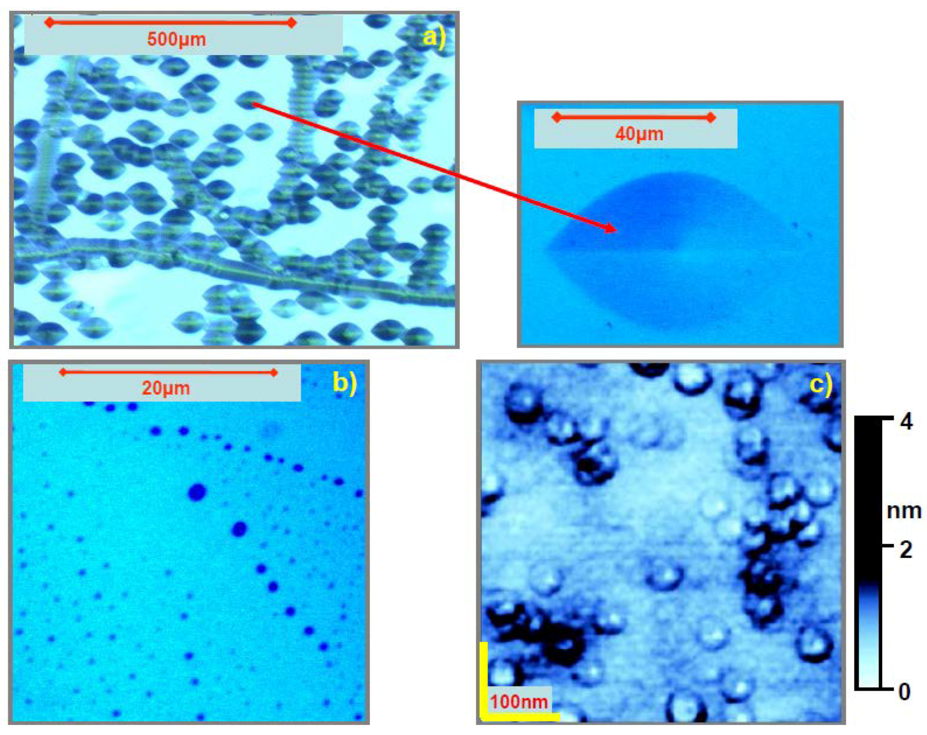
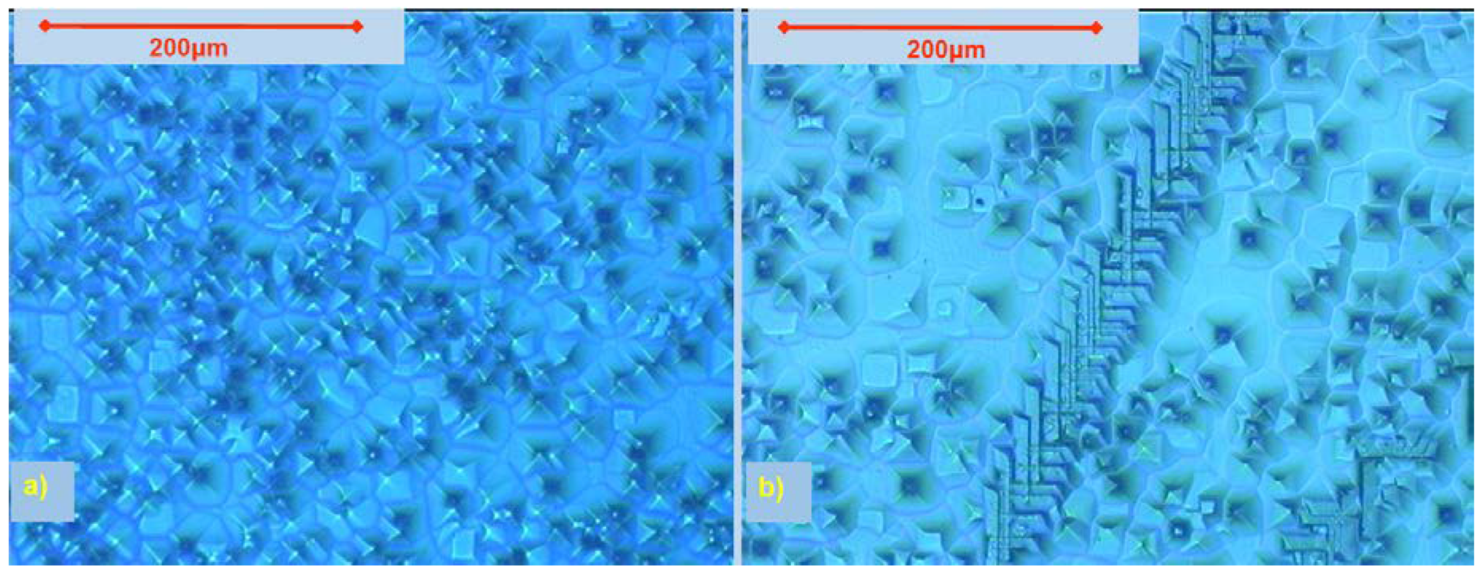
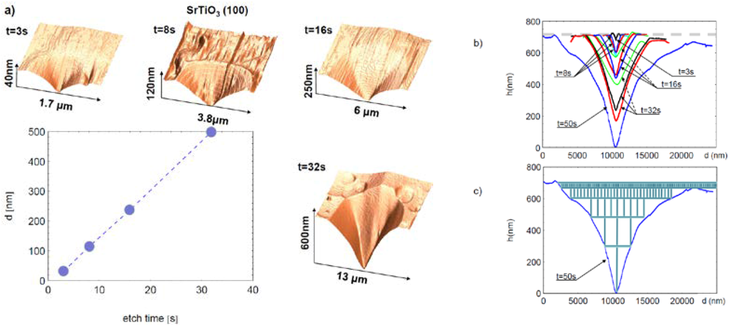
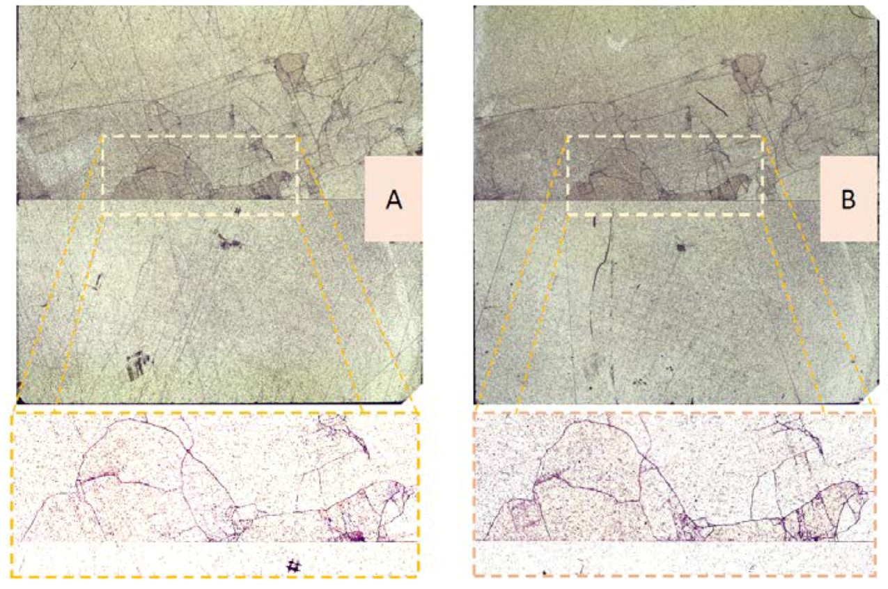
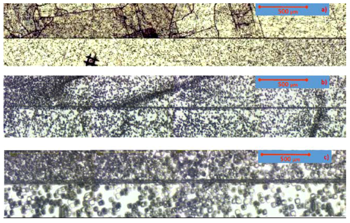
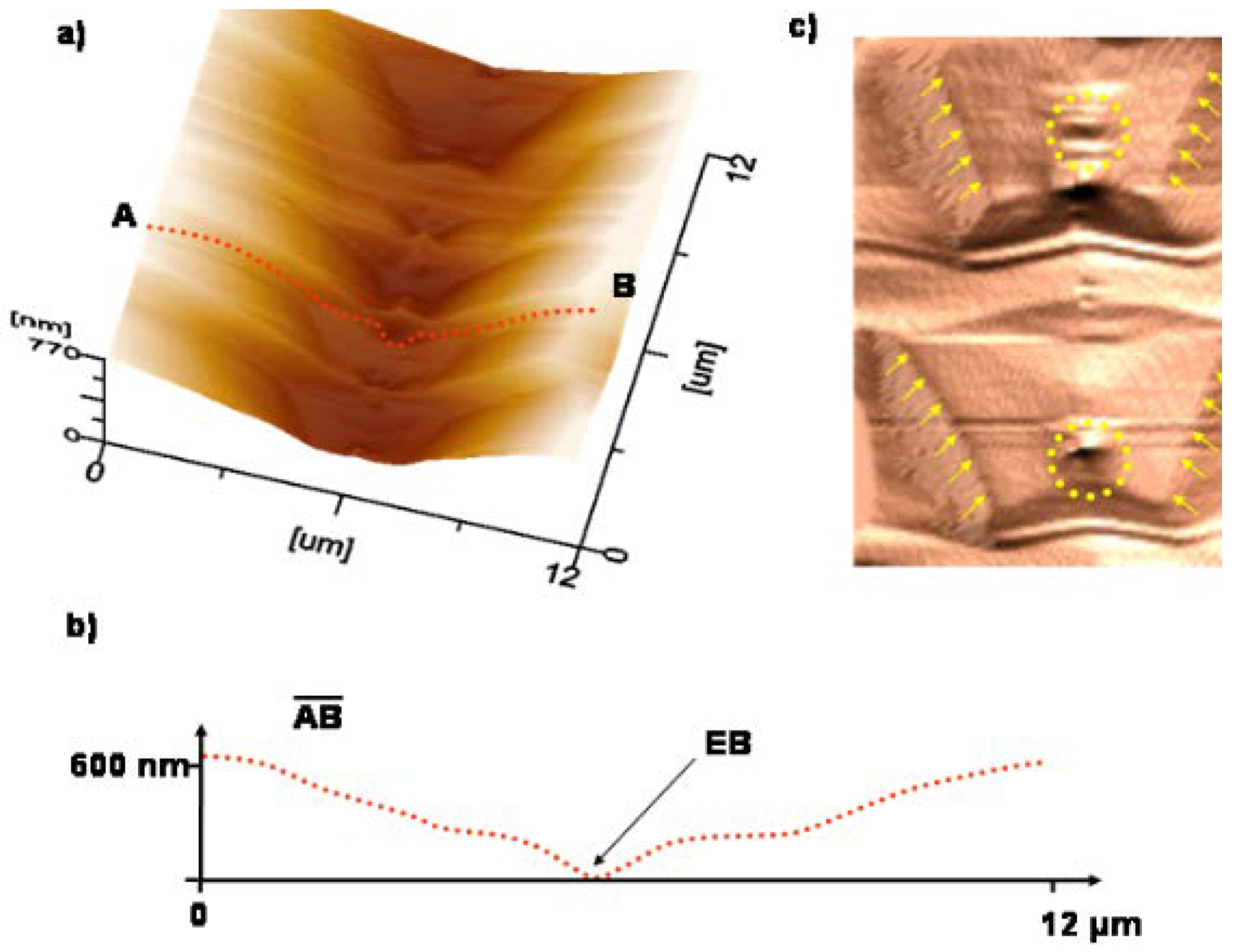
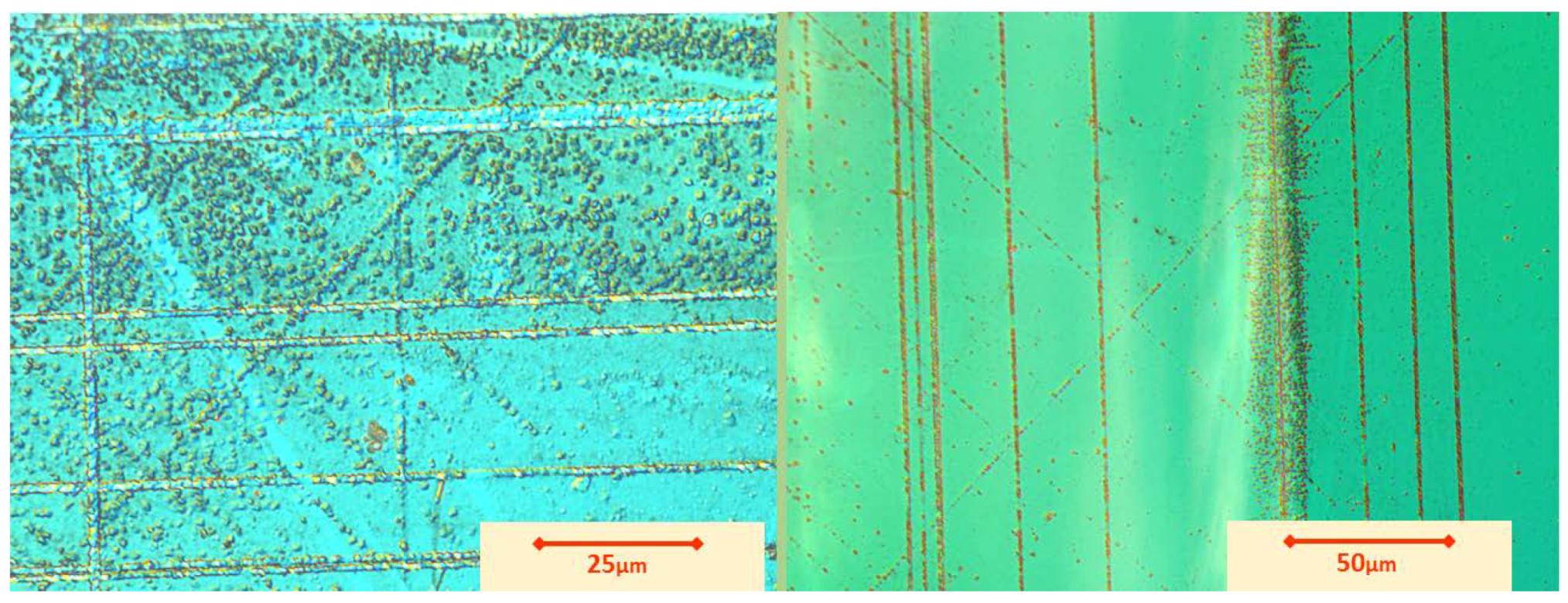
5.1. Etch Pits Technique (Optical, SEM and AFM Investigation)

Inspection of the exit of the edge dislocations in the plane of the free surface of the crystal can be obtained using an appropriate etchant. Although the connotation “appropriate” does not imply a negative meaning, it should be noted that the search for appropriate etchant has been classified as “a black art” of science. In fact, it is very difficult to define the chemical composition of the etchant for the selective decoration of the dislocations solely on the basis of theoretical considerations. Since 1953, when F. J. Vogel et al. [125] presented for the first time an unequivocal correlation between the position of dislocations and the position of the etch pits, the etch techniques has been established as a simple and popular method for the investigation of the density of dislocations, for their character (e.g., edge or spiral dislocations), crystallographic orientation and their arrangement (see, e.g., [126]). The most complicated problem which is connected with creation of etch pits concerns the nature of the selective dissolution of the surface region close to the core of dislocations. The best introduction in this problem of etch pits formation can be found in the book by Sangwal [127] who analyzed different models such as: kinematic theories, thermodynamic theories, diffusion theories, and topochemical absorption theories. Our short review cannot concentrate on a detailed analysis of each step of the etchant interaction with the core of dislocations and their surroundings. Therefore, we will only mention here that there is no plausible theory for TiO2 or SrTiO3 available which tries to correlate the creation of the nuclei (by dissolutions in etchant) caused by the preferential etching of dislocations with the available data from HRTEM techniques about of the local electronic and crystallographic structure. The important statement for this part of our review is however that etching of both model oxides does actually work!
Etching of TiO2 crystals can be realized using different etchants: HF, H3PO4, KOH, KHSO4, NaOH in a temperature regime between RT and 400 °C [28,128,129,130,131,132]. The typical wet etching with HF acid leads to the following chemical reaction, which in its character allows for preferentially decorating the exits of the dislocations on the surface of TiO2 [(100) or (110)] [132]:
Reaction:
TiO2(s) + 6HF(sol) → TiF2−6(sol) + 2H+(sol) + 2H2O(sol)
The dissolution of TiO2 in molten KOH can be described in terms of a Lux–Flood transformation (TiO2 in contact with OH ions can be fragmented into simple titanate ions) and soluble acid titanate, here K2mTinO2n+m will be formed after intercalation with K+ cations, being known as stable crystal phases in the K2O-TiO2 system [133,134].
Reaction:
TiO2 + 2 KOH → K2TiO3 + H2O
However, a simple optical inspection underestimates the density of dislocations in the surface layer of TiO2 crystal (Figure 6). In contrast, the topographic measurement using AFM shows that the real concentration of etch pits is two orders of magnitude higher than for the macroscopic (here, optical) measurement. A macroscopic inspection of the etched surface reveals different distribution of dislocations such as statistical distribution (Figure 7a) or linear distributed bundles along scratches (Figure 7b). The nano-investigation (using AFM) of the etched surface indicates that the shape of the etch pits can be round and ellipsoidal [68,128]. Notice that the AFM data show a clear tendency towards bundling of dislocations.
TiO2 + 4 KOH → K4TiO4 + 2H2O
The best results of a selective decoration of the end of dislocation lines for SrTiO3 crystals can be reached using HCl, HF or HNO3 etchants for short etching at 80–90 °C [44,45,68,135,136,137]:
SrTiO3 + 2HCl → SrCl2 + H2TiO3 → SrCl2↓ + TiO2↓ + H2O
SrTiO3 + 2HCl → H2TiO3 + SrCl2 → H2O + TiO2 + SrCl2 → TiO2 + H2O·SrCl2
2SrTiO3 + 8HF → SrF2 + H2TiO3 + SrTiF6 + 3H2O → SrF2↓ + TiO2↓ + 3H2O + SrF2 + TiF4
In the last step of this chemical treatment the crystal should be flushed with deionized water and for stopping the leaching the water should be bonded with, e.g., methanol. It should be realized that for the etching of SrTiO3 using HCl the chemical attack is in principle limited to the dislocation lines which contain a surplus of SrO. Therefore, the shape of the etch pits is round for short etching time and in fact will create a kind of pipe (see Figure 8); this shape can be easily identified by topographic investigation of the etched surface using AFM. The etching using HF produces etch pits with typical shapes of inverted pyramids (see Figure 9). The density of dislocations (for the first stage of etching), which can be calculated on the basis AFM measurements, is about 6 × 10⁹/cm2. An important conclusion which can be derived from an AFM study concerns the distribution of dislocations in-plane and out-of-plane, namely the fact that the dislocations can bundle and accumulate in <100> or <010> directions. The dramatic change of the length of segments of dislocations (analysis of the depth of the etch pits, see Figure 8) suggests that the dislocations out-of-plane are connected in a network which has a similar character than a hierarchical tree or hierarchical structure of dislocations [10,45,68]. This hierarchical structure is characterized by a high concentration of dislocations in the upper part of the surface layer and a decrease of the density towards the bulk. Further evidence of such an arrangement in a network with hierarchical structure (or alternatively hierarchical tree) is given by TEM studies out-of-plane (see Section 5.3.3), the analysis of the density of etch pits and their shapes as a function of etching time (Figure 10) and the observation of the electrical conductivity (out-of-plane) of the reduced TiO2 and SrTiO3 crystal (see below, Section 7). In the upper part of the surface layer the density of dislocations determined by TEM measurement (see e.g., [10]) is similar to the concentration of etch pits after short etching (see e.g., [45,68]). Because for both model oxides (TiO2 and SrTiO3) we were able to correlate the position of the etch pits and the position of the conducting filaments (see, e.g., [51,68]) we are convinced that the character of the change of the density of dislocations in surface region (as a function of the distance from the actual surface) corresponds with the hierarchical structure in the network. Of course, such networks have to follow the condition that in all nodes the sum of the Burgers vector should be zero. Finally, also notice that the distribution of the etch pits on the nanoscale shows a very high inhomogeneity, especially along dislocation bands (Figure 9). In such a region, the density of dislocations can even be one or two orders of magnitude higher than for the rest of the surface.
In a similar way as noted for the TiO2 investigation, an optical inspection of the etch pits density of SrTiO3 underestimates the concentration of etch pits, which is not only an effect of the resolution of an optical microscope but is connected again with the bundling of dislocations since this gives only one etch pit for a group of dislocations (Figure 10) or is caused by the hierarchical construction of the network [48]. In this case, after a short etching time, the etchant reaches a node of two or three short dislocation segments, and a prolonged etching leads to the creation of only a single etch pit. Despite the disadvantage of a microscopic investigation of etch pits in the plane of the etched surface of the SrTiO3 crystals, this technique is clearly extremely useful for a fast analysis of the distribution (homogenous, see Figure 7, or inhomogeneous as illustrated, e.g., in Figure 11) of etch pit for large areas of an etched surface.
The most impressive application of the etch technique for SrTiO3 crystals can be visualized by the distribution of the etch pits for bicrystals (see Figure 12, Figure 13, Figure 14, Figure 15 and Figure 16). Bicrystals of SrTiO3 are typically prepared by a hot-joining technique. Before joining the contact planes of the both crystals are epi-polished. The kind of temperatures used are 1400 °C and joining may last as long as 10 h, for details see [138]. For the ideal case of the distribution of dislocations along the boundary, one should only observe (after etching of the bicrystal) a kind of overlap of etch pits along a line with a distance of a few nm. Nota bene, such a configuration of the regular distribution on the nanoscale can be directly derived from the HRTEM measurement (see, e.g., [65]). Therefore, for such a position of etch pits one can expect the creation of a continuous canyon with triangular shape (considering the resolution given by an optical microscope) (see Figure 14 and Figure 15). A collection of photographs of etch pits for a bicrystal shows instead the real distributions of etch pits along the boundary and in its surroundings. For a representative presentation of etched surface, we have decided to use bicrystals of SrTiO3 with the same boundary (36.4°) originating from three different suppliers (here: Shinkosha, MaTeck and CrysTec). In our opinion, this collection demonstrates how imperfect real bicrystals can be on macroscopic dimensions. From Figure 12 one can immediately see that the densities of dislocations of both parts of the crystals are not the same (which means, that during the synthesis of both tilted parts of the crystals the dislocations in one part were more easily generated than in the other). For a simple check that the inhomogeneity has its origin in the synthesis and not by polishing one can compare the “averse” and “reverse” of the etched bicrystal (see Figure 11). Since the position of the etch pits on the top and the bottom of the crystal is the same or at least very similar, the array of dislocations seems to go through the whole thickness of the crystal. In fact, the distribution of etch pits represents a position of low and high angle boundary of the mosaic structure which has been created during synthesis (see Figure 12 and Figure 14). Such an analysis of the etch pattern is obviously helpful to extract information on the quality of real bicrystalline boundaries, revealing in the present cases the unpleasant fact that new dislocations can be created during bicrystal production (besides the boundary), dislocations also show a tendency to bundle (see Figure 13, Figure 14 and Figure 15), and, moreover, dislocations along the bicrystalline boundary and close to the boundary of the mosaic structure can agglomerate in bands. We presented these data to remind the readers that great care and experience is required to generate high-quality crystals with bicrystalline boundaries.
The classical etch technique can be successfully used for TiO2 and SrTiO3 crystals for an analysis of the change of the distribution of dislocations in-plane caused by thermal treatment (Figure 17) or mechanical stress (see below, Figure 17, right).

5.2. X-ray Topography

X-ray topography using either labor X-ray sources or synchrotron irradiation is a powerful X-ray diffraction technique for the non-destructive study of the nature and the distribution of extended defects (especially dislocations) in the plane of the surface layer and in the bulk of real crystals [139,140]. In this method, a collimated X-ray (with a shape of a ribbon) irradiates single crystals for different (selected) Bragg angles. The diffracted beam (in fact, a diffraction spot is called an X-ray topography) is analyzed via a classical X-ray sensitive photo-film or using X-ray sensitive position detectors. The influence on the local diffraction power coming from the imperfect (distorted) regions generates a variation of the intensity relatively to the perfect matrix. The manipulation of the Bragg conditions can for example be useful for the analysis of the Burgers vector of the dislocations etc. The nature of the contrast on the X-ray topography is described by the kinematical and dynamical theories of X-ray diffraction [141].
This very sensitive method for the analysis of the extended defects and strained regions has often been used for SrTiO3 crystals, especially for studies of the mosaicity and the density of dislocations which are generated during growth of the crystals with different methods [99,100,101,102,103,104,142,143]. It should be noted that the X-ray topography studies for SrTiO3 crystals have revealed that these crystals cannot be (in the regular phase) classified as a monocrystals, because the low- and high-angle boundary are typical for the mosaic-like structure, which in turn means that such crystals can be defined as single crystals.
In contrast to the detailed study using X-ray topography of SrTiO3 crystals there is no literature about this topic for TiO2 crystals.

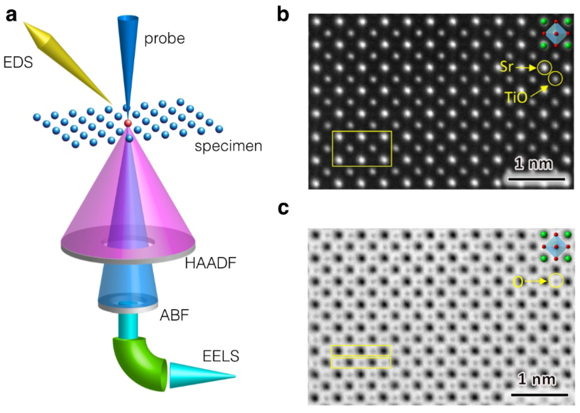
5.3. Imaging and Spectroscopy by Atomic-Resolution STEM

In order to investigate the structure and chemistry of dislocation cores, it is necessary to employ a new tool to directly observe the local atomic configurations, chemical types and their electronic structures. One of the most versatile experimental systems for this purpose is an electron microscope and we briefly describe in this section the concepts and the ability of modern electron microscopy. Following the successful implementation of 3rd or 5th order aberration correctors in electron microscopy [144,145], the spatial resolution has dramatically improved and the current attainable lateral resolution is 40.5 pm—less than half an Ångström [146]. In addition to the progress on electron optics, the mechanics and electronics and detectors have been significantly improved which allows us to perform electron energy-loss spectroscopy (EELS) [147,148,149] and energy dispersive X-ray spectroscopy (EDS) [150,151] at atomic dimensions. There is a wide variety of microscopy, and two major systems in atomic-resolution are well known: transmission electron microscopy (TEM) and scanning transmission electron microscopy (STEM). In the nature of great flexibility of detectors, we here introduce the currently widespread imaging and spectroscopy of modern STEM.
In history, STEM was invented and designed by M. von Ardenne in 1937, which is only several years behind the development of TEM by M. Knoll and E. Ruska in 1932 (detailed can be found in this book [152]). However, there were many technical difficulties (mostly limited by noise) of STEM and then most of efforts were dedicated on the development of TEM. In the late 1960s, A. Crewe newly designed and constructed STEM with a field emission gun, annular detector and spectrometer for EELS, where the transmitted electrons through the center hole of annular detector were collected by the EELS spectrometer [153]. The basic design of modern STEM is referred to Crewe’s microscope. In 1970s, Crewe firstly achieved the visualization of single Uranium atoms on thin amorphous carbon films [154]. In late 1980s, STEM technique was applied to the crystal viewed along the low index crystal orientation and firstly realized the chemical sensitive imaging in the crystal, where the annular dark field (ADF) detector was set at high-angle to efficiently remove elastic scattering contrast [155]. This imaging mode is known as high-angle annular dark-field (HAADF), where the contrast is sensitive to the constituent atomic number (Z) and therefore the mode is also known as Z-contrast imaging.
Hardware of the modern STEM. Figure 18 shows the schematic view of STEM configuration and detector geometry. The imaging electrons are generated by a field emission gun, and the electrons are very finely focused by the aberration correctors and probe forming objective lens. Then, the sub-ångström electron probe is scanning over the specimen and the atomically resolved images are formed by collecting the transmitted electrons at each probe position with detectors beneath the sample.
Typical description for each component is given as follows. Incident electrons are typically accelerated at 60–300 keV and relatively higher accelerate voltages such as 200–300 keV are typically selected for oxide materials because of higher spatial resolution. Lower accelerate voltages of 60–80 keV are also commercially available and used for the observation of two-dimensional materials, i.e., graphene or transition metal dichalcogenides [156]. The energy spread of the incident electrons are typically ΔE ~ 0.4 eV with a cold field emission gun, which is enough to perform core-loss EELS measurements. Recent progress on the monochromator of an electron source, the energy resolution is greatly improved up to 10–30 meV (10 times better than that of a cold field emission gun), which makes it possible to measure the local bandgap and phonon excitation (vibrational spectroscopy) [157,158]. The most limiting factor for atomic-resolution imaging was 3rd order spherical aberration but at the end of last century the combination of multi-pole lens system (quadra-octa poles or hexapole lens system) solved the problem, the invention of aberration correctors. Using an aberration corrector, the illumination angle in STEM is typically increased 20–30 mrad (semi-angle), providing sub-ångström probe. For detection of transmitted electrons, scintillators (Ce-doped YAP) combined with photomultiplier tubes are mostly adapted for the imaging detectors because short life time (~30 ns) at room temperature and moreover it is sensitive to single electron levels [159]. Recently, the shape of detectors is reconsidered, and segmented-type [160,161] and pixelated-type detectors [162] are now used for electromagnetic field imaging and ptychographic imaging. In this section, we will briefly describe the imaging and spectroscopy of HAADF, ABF (annular bright-field), EDS and EELS, respectively.
High-Angle Annular Dark-Field: HAADF. Using an aberration corrector and objective lens, the image of a gun tip or probe is formed on the specimen surface or preferable location. The wave function of the probe at the position r p in real space (r) is given by the illumination angle ( α m a x = λ k m a x ) and the aberration wave function exp [ i χ ( k ) ] in reciprocal space (k) [163]:
Ψ ( r , r p ) = A 0 k m a x exp [ i χ ( k ) 2 π i k ( r r p ) ] d k .
The aberration correctors are operated to maximize the aberration wave function in a wide range of k-frequency and the probe size becomes smaller than 0.1 nm. The probe is then scanned across the sample and the transmitted electrons are used to form atomic-resolution images. The image intensity and accessible information depend on the location of the detector in reciprocal space:
I ( r p ) = | Ψ t ( k ,   r p ) | 2 D ( k ) d k ,
where Ψ t ( k , r p ) . is a Fourier transformation of the transmitted wave function, and D ( k ) is detector function (1: on the detector and 0: otherwise). The detector shape is usually radially symmetric such as circular or annular detectors. The inner angle of the HAADF detector is typically twice higher than the illumination angle, e.g., the integration range is 60–200 mrad for the illumination angle of 30 mrad. In such high-angle condition, the amount of elastically scattered electrons is progressively reduced and incoherently scattered electrons are the dominant contribution of the image: the thermal diffuse scattering related to Debye-Waller factor rather than coherent Bragg scattering [164,165]. The electrons at high-angles were scattered nearly from the nuclei and the contrast in HAADF shows the Z2-dependence of unscreened Rutherford scattering and the HAADF STEM is called Z-contrast imaging. In this sense, the intensity of HAADF image may be simply described by the straightforward convolution of point spread function P(rp) and objective function O(rp):
I H A A D F ( r p ) = P ( r p ) O ( r p ) .
Figure 18b shows the HAADF STEM image of SrTiO3 viewed along the [001] direction, and one can clearly recognize the locations of Sr and Ti-O atomic columns, as respective bright contrasts [166]. Owing to the Z-contrast nature, the heavier Sr atomic column is brighter than Ti-O atomic column, and therefore Z-contrast imaging can be considered as a chemical sensitive imaging. The other advantage of HAADF image is non-reversal contrast, i.e., the atom position appears as a bright dot contrast even with relatively thick specimen of 50–100 nm, providing a simple interpretation of the image. Although it requires full dynamical image simulation, it is now possible to quantify the intensity of HAADF image or even count the number of atoms in projection [167,168,169,170].
Annular Bright-Field: ABF. HAADF STEM is quite powerful and solves a number of materials’ problems [152]. It is however hard to recognize light atom positions in HAADF STEM because of the low scattering power of the light elements into high-angles. In oxide materials community, the identification of oxygen atom position has long been desired to understand the origin of physical properties such as ionic conductivity, superconducting, ferroelectricity and ferromagnetism. After the implementation of aberration corrector, the bright field region (the smaller scattering angle than the illumination angle) has been reconsidered and a new method of annular bright-field imaging was proposed with the aid of comprehensive theoretical investigations [171,172]. As shown in Figure 18a, ABF detector is placed at the bright-field region but the half of central regime is not used for imaging, i.e., detection angle is 15–30 mrad with the illumination angle of 30 mrad. Figure 18c shows the ABF STEM image of SrTiO3 viewed along the [100] orientation, simultaneously recorded with HAADF STEM. In ABF image, the atomic column can be seen as dark contrast that is opposite contrast of HAADF image, but the atom positions in ABF image are exactly the same as HAADF image. In addition to Sr and Ti–O atomic column, new dark contrasts appear in ABF image, corresponding to the oxygen atom positions. In bright-field region, there appears electron scattering interference between transmitted and scattered waves, which may produce the artefact contrast eventually at the oxygen atom positions. To establish the robustness of ABF STEM imaging, deliberate theoretical investigations have been performed, including various crystal systems, defocus-thickness dependence, specimen tilt, detector misalignment and non-uniformity of the detector response [172,173]. Although the image formation mechanism of ABF STEM is not as simple as HAADF STEM, it realized that the dark contrasts can universally be observed at the light element atomic positions. It is noteworthy that, under the in-focus condition, the atom positions of both heavy and light elements can be seen as non-reversal dark contrasts, and therefore ABF STEM imaging is directly interpretable and as robust as HAADF STEM imaging.
Here we describe the image formation mechanism of ABF STEM in a simplified manner [174]. When the probe is traveling through the heavy atomic column, the electrons are channeling along the column and most of electrons are scattered into dark-field regime, visualizing the heavy atomic column as a strong dark contrast. While at the light atomic column, the electrons are weakly channeling along the column and a part of electrons are scattered forward and go through the central hole, and therefore the light atomic column becomes faint dark contrast.
Although we explain the robustness of ABF STEM imaging but the remaining intriguing question is whether the lighter atoms than oxygen is possible to detect in ABF imaging. As an example, Figure 19 shows the simultaneously recorded HAADF and ABF STEM images of LiCoO2 viewed along the [100] crystallographic orientation [174]. In HAADF image, one can see only the Co atoms as a bright contrast and the other atoms of oxygen and Li are difficult to recognize. However, in ABF image, all the chemical types of atoms are visible as dark contrast including Li atoms. ABF imaging has been used to lithium ion battery and hydrogen storage materials and successfully achieved the visualization of lithium [175] and even the lightest element of hydrogen atomic column [176,177]. Therefore, it is possible to visualize all the chemical type of elements at atomic dimension.
Electron Energy-Loss Spectroscopy: EELS. In metal oxides, transition metals possess a wide variety of valence states that directly dictate the physical and chemical properties. However, the intensity of HAADF and ABF images is insensitive to the valence state of transition metals and another approach is required to identify the local electronic structures. When high-energy incident electrons pass through the specimen, the incident electron may interact with atomic electrons surrounding a nucleus, which process is known as inelastic scattering. The core electrons of the constituent atom will then be excited to the outer shell and the incident electrons conversely lose the corresponding energy. EELS can typically measure the loss-energy of the incident electron in the range of less than 3000 eV, which allows us to determine the valence state (>200 eV), plasma excitation (10–30 eV), band gap (<10 eV), and phonon vibration (10~100 meV). The cross-section of inelastic scattering may be written as a dynamic form factor S(q, E) [178]:
2 σ E Ω S ( q , E ) = i , f | ϕ f | e i q r | ϕ i | δ ( ε f ε i E ) ,
where | ϕ i > is the initial core state of energy and momentum ( ε i ,   k 0 ) , | ϕ f > is the final conduction state of energy and momentum ( ε f ,   k ) for the electron of the constituent atom, the transferred momentum is q =k0k. It is noteworthy that, as illustrated in Figure 18a, EELS measurement in STEM is compatible with HAADF STEM imaging because the most of inelastic (forward) scattering electrons can go through the central hole of HAADF detector.
Figure 20 shows an example of the line scan of Ti-L2,3 edges (STEM-EELS) obtained from the photocatalytic materials of LaTiO2N from the surface to the bulk (1 nm step) [179]. In the bulk, two peaks split into four peaks (t2g and eg states) and the valence state of Ti is identified to be 4+. While in the near surface (<2 nm), two peaks are not split and therefore the valence state of Ti is 3+ only at the surface and this region is active in photocatalytic reaction.
In STEM mode, the EELS data acquisition is not limited to line scan profile but is possible to perform in 2D scan. Although the acquisition time is at least three orders of magnitudes slower than ADF imaging, the higher mechanical stability of modern STEM makes it possible to acquire spatially resolved 3D data cube at atomic-scale, where EEL spectrum is obtained at 2D probe position. On the basis of post data analysis, atomically resolved chemical mapping and moreover valence mapping are possible, although the channeling condition is carefully considered for the interpretation of data set [147,148,149]. In this section, we have discussed the valence state of transition metal, but the EELS has more capability: measurement of the specimen thickness (log-ratio method), estimation of local concentration of vacancy, valence EELS, vibrational EELS [178].
Energy Dispersive X-ray Spectroscopy: EDS. When the constituent atom of a specimen is excited by the high energy electron beam, an electron hole is created in the inner shell. The excited electron then refills the hole and the specific energy (difference between inner and outer shells) is then released in the form of an X-ray. Generated specific-energy X-ray is directly related to the chemical type and therefore it is useful to determine the chemical composition of a specimen. The cross-section in EDS is typically three orders of magnitudes smaller than that of EELS and moreover a collection solid angle of EDS detector was ~0.1 sr (a sphere is 4 π sr), which has long been the technical difficulty to perform atomic-resolution EDS mapping. Recently, a considerably large size of silicon drift detector (>100 mm2) has been introduced and the solid angle is significantly increased to 1.0 sr. Furthermore, using multiple silicon drift detectors, the total solid angle is now larger than 2.0 sr. To understand the measurement system, we here compare the methodology of EDS to EELS. The measurable energy range in EELS is less than 2 or 3 keV, whereas EDS can perform in much wider range from 0.1 eV to 30 keV, and therefore EDS can detect all the chemical types, except for the lighter elements like lithium. While in the energy resolution, EELS has much high energy resolution than that of EDS, and EELS is suitable to investigate fine electronic structure of materials. In EDS, silicon drift detector is connected to a pulse processer (incoming voltages convert into counts) and processing is very fast. The EDS detector can wait for eventual X-rays, and therefore multiple-frame scanning can easily perform as used in STEM imaging to enhance signal-to-noise ratio. While in EELS, the read-out time is considerably slow in charged-couple devise and moreover a reading-out noise is introduced for each time and therefore one-time measurement is suitable. Considering the beam damage issue, EDS with fast multiple scanning would be suitable for the compositional mapping at atomic-scale.
Figure 21 shows atomic-resolution HAADF and EDS images of a single dislocation core at the low-angle tilt grain boundary of Mn-doped SrTiO3, where the crystallographic orientation is (100)/[001] with a 5° mistilt angle [180]. After the acquisition of EDS spectra at each probe position, Mn-L, Sr-L, Ti-K edges were integrated and the then EDS maps were obtained. It can be clearly seen the Sr and Ti columns are spatially resolved in EDS maps. At the dislocation core, Sr becomes slightly depleted and it is then realized that Mn dopants substituted Sr combining with EELS analysis.

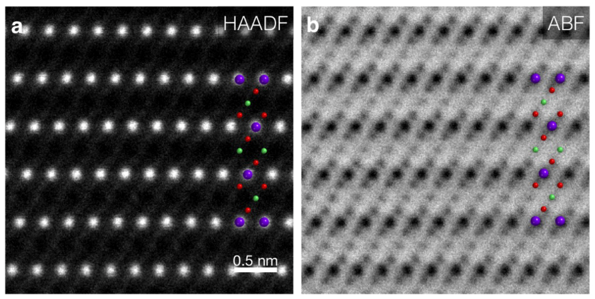
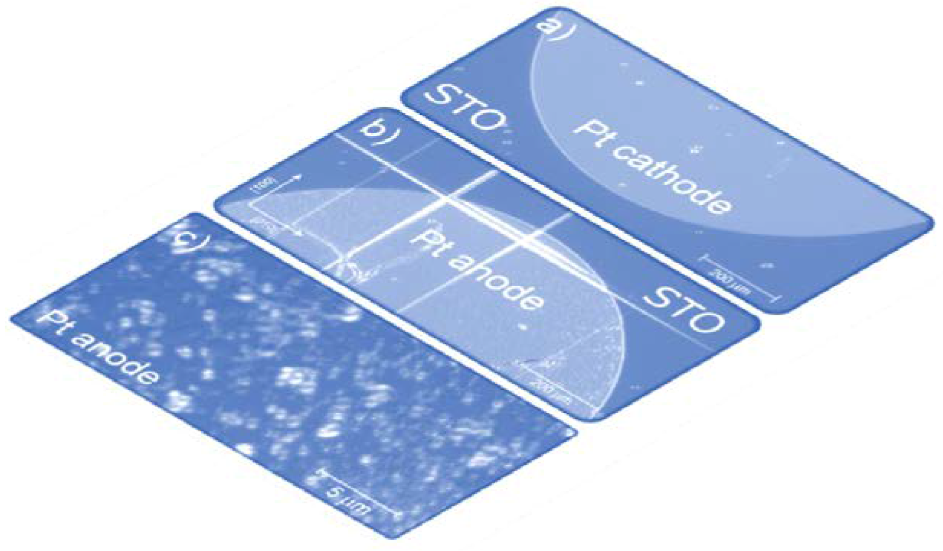
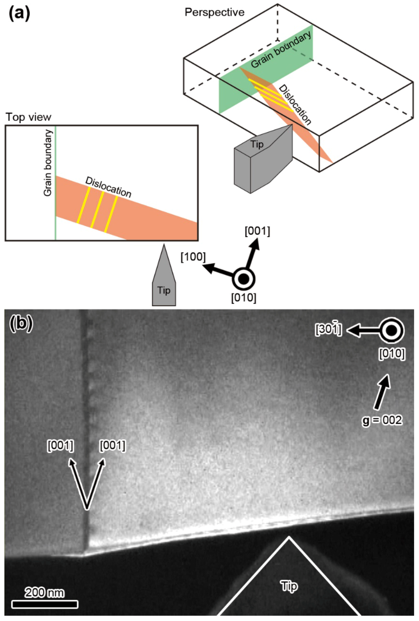
5.3.1. Dislocation Structure and Chemistry in the Grain Boundary of SrTiO3

A dislocation is a one-dimensional crystal defect and has so far been investigated to understand the mechanism of deformation or mechanical properties in metals. In semiconductor and insulator materials, however, we may have an opportunity to embed a new functionality in dislocations, especially electric [3], magnetic [180,181] and optoelectronic properties. For further development of functional dislocations, it is a prerequisite to identify the chemistry and atomic/electronic structures of dislocation cores. To perform comprehensive investigations on a dislocation, it is desirable to fabricate well-defined dislocations. One appreciable approach is the bicrystal method, where two single crystals are thermally bonded in a specific crystal orientation. In a low-angle tilt grain boundary, dislocations are periodically introduced along the grain boundary to compensate the mis-tilt. In this section, we will discuss a specific example of SrTiO3 dislocation core structure, especially on the dislocation core structure in the grain boundary rather than the dislocations in the bulk, by using modern atomic-resolution STEM [95].
The SrTiO3 bicrystal with a [001]/(100) 10° tilt grain boundary was prepared by a thermal diffusion bonding of two single crystals, where the bicrystal was finally annealed at 1000 °C for 80 h after the pre-annealing at 700 °C for 20 h. The electron transparent TEM sample was prepared by conventional mechanical polishing and subsequent Ar ion milling with lower voltage of 0.2 kV. Figure 22a shows HAADF STEM image obtained from the bicrystal viewed along the [001] crystal orientation. There are two types of dislocation cores are alternatively arrayed along the grain boundary, and we will denote these dislocation core structures as core-A (SrO-termination) and core-B (TiO2 termination), respectively. The distance between these cores are about 6 unit cells which is consistent with Frank’s formula calculated from the mistilt of 10°. The Burgers vector of these cores are the same as a [100], but the observed Z-contrast has much difference: the contrast of the core-B is much darker than that of the core-A. Figure 22b–e shows simultaneously recorded enlarged HAADF and ABF STEM images of core-A and core-B, respectively, where oxygen atomic columns in ABF images are also visible as a dark faint contrast even at the dislocation cores. The corners at the dashed white lines are TiO and Sr atomic columns for core-A and core-B, respectively. Some oxygen atomic columns have low occupations and moreover at the center of core-A, the oxygen atomic column is completely missing. At the cation site in these cores, some atomic columns exhibit the contrast elongation or split, suggesting local structure inhomogeneity. To precisely identify the dislocation cores, it is necessary to determine the elemental distribution at the dislocation cores.
Figure 23a shows atomic-resolution EDS maps at the dislocation cores (red: Sr, green: Ti), where 10 pair of dislocations core maps were averaged to minimize the spatial variety and improve signal-to-noise ratio. The enlarged EDS maps of core-A, -B are shown in Figure 23b,c, respectively, where the dashed lines correspond to the location in Figure 22. As expected from the HAADF and ABF images, the atomic structure of core-A seems to be simple: no mixture of Sr and Ti and the three Sr columns at the core-A have slightly small occupation. While in the core-B, Sr occupation seems to be poor and Ti signals are widespread at the dislocation core region (not sharp contrast). Combining Ti EDS map with ABF image, it is realized that the reconstruction is related to a transition of TiO6 octahedrons from corner sharing in perovskite to edge sharing: the local formation of rocksalt-like structure. Since the probe channeling effects along the atomic column always disturb the quantification of EDS signals, we here use a linear approximation of EDS signals [182], which provides a rough estimation of the local composition. The elemental occupations of the dislocation cores are estimated to be (Sr, Ti) ≃ (0.82, 085) for the core-A and (Sr, Ti) ≃ (0.63, 0.90) for the core-B, respectively. On the basis of these analysis, we identify the local composition of at each atomic column for both dislocation cores, and the results are given in Figure 23b,c, as overlaid structure models, where the numbers are indices for atomic columns and the color corresponds to the occupation of elements (red: Sr, green: Ti, yellow: O, while: unoccupied). At the core-A, the oxygen columns of #11 and #12 have very low occupations. At the core-B, most of Sr columns of #13, #14, #18, #19, #21 are partially occupied by Ti atoms and some oxygen atomic columns, expected from the bulk extrapolation, are also occupied by Ti, which gives an impression of very green-colored EDS map at the core-B.
In addition to the composition, the electrical activity of dislocation core is also strongly affected by the local electronic structure of Ti, which can be measured in EELS. Figure 24a shows EEL spectra obtained from the core-A, core-B, gap between A and B (continuously connected two single crystals at the grain boundary), and the bulk region, respectively. In SrTiO3, the two peaks of the Ti-L edge for Ti4+ are well splitting into four peaks, corresponding to the eg and t2g states respectively. At both the dislocation core regions, Ti-L edges show slight energy shift towards lower energy and less pronounced peak splitting, suggesting the mixture of Ti3+ and Ti4+. Using multiple linear least squares fitting, the spatial distribution of Ti valence states are determined and given in Figure 24b,c for Ti3+ and Ti4+, respectively. The slightly reduced Ti3+ regions are concentrated at the dislocation core regions, while the bulk and gap regions maintain the valence state of Ti4+. Combining atomic-resolution HAADF, ABF imaging and EDS, EELS spectroscopy, the dislocation core-A and core-B is estimated to be Sr0.82Ti0.85O3−x (Ti3.67+; 0.48 < x < 0.91), and Sr0.63Ti0.90O3−y (Ti3.6+, 0.57 < y < 1), respectively. To possess the charge neutrality at the dislocation cores, the amount of the oxygen vacancies is estimated to be x = 0.63, and y = 0.75.
In general, the oxygen vacancy formation energy is significantly reduced at the dislocation core, which is true in this case of core-A and core-B. For the dislocation core-A, the occupation of the oxygen columns of #11, #12 is considerably small because of strong Coulomb repulsive interaction between these two neighboring oxygen columns. For the core-B, oxygen columns are replaced by Ti, which is originated to the TiO2 plane termination at this core. The observed oxygen deficiency results in the reduction of Ti valence, which is also confirmed by EELS. Compared with bulk SrTiO3, the reduced Ti ion may contribute to the local electrical conductivity along the dislocation cores. Oxygen vacancies also introduce some spaces and therefore oxygen ion conductivity may be enhanced along the dislocation cores. The composition of dislocation core can be expressed as αSrO·βTiO2·γTi2O3 (Ti3+ for Ti2O3, Ti4+ for TiO2), where α and β + γ can be measured from the EDS mapping of Sr and Ti and the ratio of β to γ can be estimated from the EELS. From the experimental results, the respective components for the core-A and core-B are determined to be (α, β, γ)A = (0.82, 0.57, 0.14), (α, β, γ)B = (0.63, 0.54, 0.18). Since the dislocation cores are different from the bulk in the sense of crystallography and chemistry, the dislocation cores should be probably considered as foreign objects when we discuss the local properties of electric or ionic conductivity. Therefore, a simple space charge model without consideration of the presence of these foreign objects is no longer sufficient to precisely interpret the local properties at the dislocation cores.

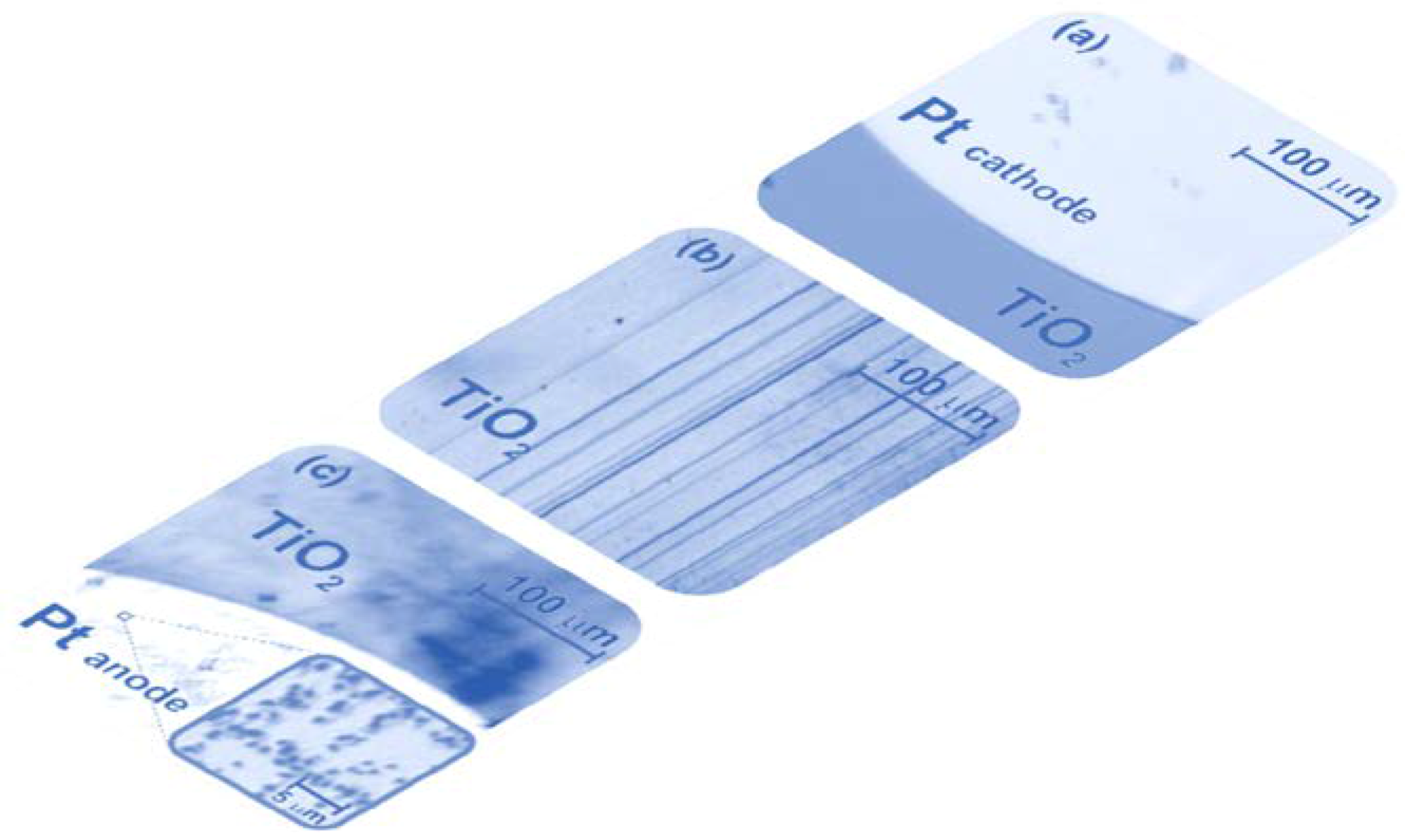
5.3.2. Dislocation Structure and Chemistry of Titanium Dioxide (TiO2)

TiO2 has been intensively investigated for long time because it shows potential applications in a wide range of industrial fields, including catalysis, photocatalysis, sensors, solar cells [183,184,185,186]. It also shows the properties as a wide-band-gap (3 eV) semiconductor, but many of its applications can be enhanced by additional electrons that originate from the defect states in the forbidden band gap [187,188]. Different explanations of these states are possible, e.g., such in-gap states have been observed in DFT calculations originating from edge dislocations or extended defects [32,48]. An understanding of their origin is therefore critical to improve the functional properties of TiO2 because dislocations are implicated in many applications [189,190]. It has been reported that dislocations are existent on the {101}, {110} and {100} planes in rutile TiO2 [22,27,191,192]. The plastic deformation in rutile TiO2 was also found to take place by activating {101}<10 1 ¯ > and {100}<0 1 ¯ 0> slip systems [192]. The dislocations have been confirmed to affect the electrical properties of TiO2 single crystals [19] and the ionic conductivity of polycrystalline TiO2 [20]. However, the relationship between the dislocation core structures and properties is still unclear because the general knowledge on the atomic-structures of dislocations has not been well characterized. In this chapter, atom-resolved imaging is demonstrated for the core structure of <001> dislocation in TiO2 bicrystals [32] by Cs-corrected STEM.
It has been known that the <001> and <101> dislocations can be introduced into TiO2 crystals [37]. However, the naturally or plastically introduced dislocations are usually wavy and it is not so straight to directly resolve their core structures at the edge-on condition by TEM. In this study, by using bicrystal technique, the low angle tilt grain boundaries, which contain periodic array of straight edge dislocations, were fabricated to directly observe the core structure of TiO2 [32,193,194]. In this case, all atomic columns can be identified from the [1 1 ¯ 0] direction. For these reasons, the <001> edge dislocation was selected as a model system. The TiO2 bicrystals with a small tilt angle of about 5 degree were fabricated by precisely joining two pristine single-crystal blocks of high purity rutile TiO2 from the orientation relationships (110)[001]//(110)[001] [32]. To prepare the bicrystals with an array of periodic dislocations, two single crystals were cut by 2.5 degree from the (110) plane of the TiO2 single crystal, followed by the mechanical grinding and polishing of the contact planes to a mirror finish. The two surfaces were bonded with the [001] direction of one crystal almost parallel to [001] direction of the other by a small tilt angle of 5 degree (2.5 degree + 2.5 degree) under hot pressing at 1773 K for 10 h in air. TEM and STEM specimens were prepared by cutting, grinding, dimpling and argon ion-beam thinning. HAADF and ABF images were taken using the Cs-corrected ARM-200FC (JEOL, Ltd., Tokyo, Japan) STEM operated at 200 kV, which provides a small probe size less than 0.1 nm. The ABF STEM images were observed with a detector of 12–24 mrad, and EELS spectra were recorded using the Gatan Enfina system equipped on the STEM with an energy resolution, at full-width of half-maximum, of about 0.5 eV.
To confirm the orientation relationship of the bicrystal and clarify whether dislocations are introduced into the boundary area, the selected-area diffraction pattern (SADP) was taken (Figure 25a) together with STEM image (Figure 25b) of the boundary area in the 5 degrees [001] bicrystal, in which the incident electron beam is parallel the [110] direction. An overall symmetry is clearly seen in the pattern, and a slight visible splitting is revealed for some diffraction spots (Figure 25a). In light of the splitting spots in the SADP, the tilt angle (θ) of the bicrystal is estimated to be 5.1 degree, indicating a successful joining of the bicrystal with the prescribed orientation relationships. As seen in Figure 25b, the periodic image contrast exactly on the mirror plane of the (110)[001] boundary, suggesting the formation of an array of dislocations at the boundary. The dislocation core structures are expected to be observed at edge-on condition. It can be thus said that the two crystals are well bonded with no secondary-phase layers, amorphous layers, contaminants, or transitional areas at the boundary region.
Figure 26a shows HAADF STEM image of a typical dislocation projected along the [110] direction. Considering the contrast and the crystal structure, the brightest spots represent Ti–O mixed columns, which unravel an almost symmetric core geometry for the edge dislocation of TiO2. It was found that all of the dislocations showed the identical core configuration. The core region is slightly darkened owing to the strain associated with the dislocation. In addition, the considerably lighter O atoms are not scattered strongly enough to be visualized. As mentioned in the previous section, ABF STEM imaging technique has an advantage to directly observe light atoms. Figure 26b shows ABF STEM image of the same area of Figure 26a, where only the Ti–O mixed column and the pure Ti column are observed from this projective direction.
In order to evaluate the electronic structures of a single dislocation, atomic resolution EELS analyses were conducted for the Ti-L2,3 edge for the dislocation core region together with that of the bulk as a reference (figure 27). It is clearly shown that Ti-L2,3 EELS spectrum in the region away from the dislocation core (close to the bulk) mainly consists of four peaks (i.e., two doublets), where one doublet at lower energy loss comprises the Ti-L3 edge, whereas the other at the higher energy loss Ti-L2 edge shows the characteristic of having a valence state of +4 for the Ti atoms away from the core [195]. In contrast, the Ti-L2,3 EELS spectrum taken at the core area exhibits a broader profile (marked by arrows in Figure 27), suggesting that they are of a mixed valence state of +3/+4 because the main difference in the Ti-L2,3 EELS spectrum between Ti4+ and Ti3+ rests with the broadening of the t2g peaks in each doublet. We further conducted EELS measurements over a broad energy span and found that only the signatures of Ti-L2,3 and O-K edges are detected both at the core and in bulk, providing evidence that a substantial segregation of impurity to the core can be ruled out, i.e., the dislocation core is impurity free. Such a shift in electronic states indicates the formation of a conducting channel at an individual dislocation and points to the existence of novel impacts associated with the impurity-free dislocations of TiO2 [32].

5.3.3. Hierarchical Distribution of Dislocations in the Surface Layer of SrTiO3

The TEM investigations on the distribution of the dislocations in the surface region of SrTiO3 crystal (as received) show a progressive lowering of the dislocations density (Figure 28) going from the surface towards the interior [10]. Depending on the polishing procedure the density can vary from 4 × 10⁹ – 6 × 10⁹ (for the epi-ready polished surface [10,68]) to 1012 for the rough surface [42]. Such tendency in the distribution of the dislocations in the surface region (thickness of about few dozen μm) allows to analyze this system in terms of a hierarchical network, which fulfills the criterion that the sum of the Burgers vector of the dislocations in each of the nodes is zero. On the basis of the depth dependence of the density of dislocations a schematic view of the mentioned network has been created [68]. Strong reduction of the density of dislocations in the upper part of the network forces that the dislocations near the surface should be very short (only a few nm) while the length of the dislocations line between deeper nodes becomes successively longer. Jin et al. [42] showed that the dislocations in surface region exist not only as individual dislocations, but that these dislocations have a tendency to create a pair or agglomerate in form of bundles.

5.4. Electron Channeling Contrast Imaging (ECCI)

Electron channeling contrast imaging (ECCI) combines the classical scanning electron microscopy (SEM) with the simultaneous analysis of backscattered electrons. This technique can be used for the investigation of extended defects such as dislocations or stacking faults, in crystalline samples or in polycrystalline materials (only for single grains). In principle, the penetration depth of this method is limited by the escape depth of backscattered electrons. The interaction of the electron beam can be described in terms of the standing electron-density waves which are formed in the matrix of the electron-irradiated crystal. The intensity of the backscattered electrons is influenced by the position of the nuclei in the lattice and the orientation of the lattice relatively to the primary beam. The minimum of the backscattering can be observed for the orientation between beam and lattice plane when the Bragg conditions are fulfilled. That means that similar than for TEM techniques for the identification of the dislocations the classical invisibility criterion namely (g·b = 0) can be used [196,197,198,199]. In other cases, the electron can be channeled in deeper parts of the crystal without strong interaction with the matrix. For extended defects the channeling of electrons into the interior of the crystal is strongly reduced; therefore, the backscattered electrons are carriers of information about the position of the defects and their type (Figure 29).

5.5. Electron Holography

In electron holography, the complex wave function (that means the amplitude and the phase) of fast electrons which are transmitted through a thin foil during TEM investigation is analyzed [92]. Because it is impossible to detect the phase of the electron wave function directly, since it can be modified by local electrostatic and magnetic fields, two indirect techniques for the reconstruction of the phase modulation are used namely the off-axis and the inline method. In the off-axis method, the electron beam is split by an electron bi-prism into one part traveling through the specimen and one part passing through vacuum which are then brought to interference. In inline holography, the specimen is placed in the divergent electron beam such that only one part of the beam interacts with the object and an interference with the undistorted part of the same beam occurs. In both cases, the phase then can be calculated from the recorded interference pattern [201].
Because this technique has a very high lateral resolution, it can be used for the study of the local potential distribution especially in the interface [90,91,92,93]. The prime example for the application of this technique is the analysis of the potential change close to the small boundary in SrTiO3 crystals with and without doping. It is surprising that the thickness of the barrier is only 1–2 nm (without influence of the doping) (Figure 30). The potential drop is about 0.45 V for the barrier in the Nb doped bicrystal and −0.6 V for the barrier in the undoped crystal [92]. This barrier can be annihilated using appropriate polarization (perpendicular to the barrier) probably via local breakdown. Notice, such a change of the potential (+0.45 V or −0.6 V) on the small distances of just 2 nm actually creates a local electrical field of the order of 106 V/cm, high enough for a cold emission of electronic carriers according to literature.

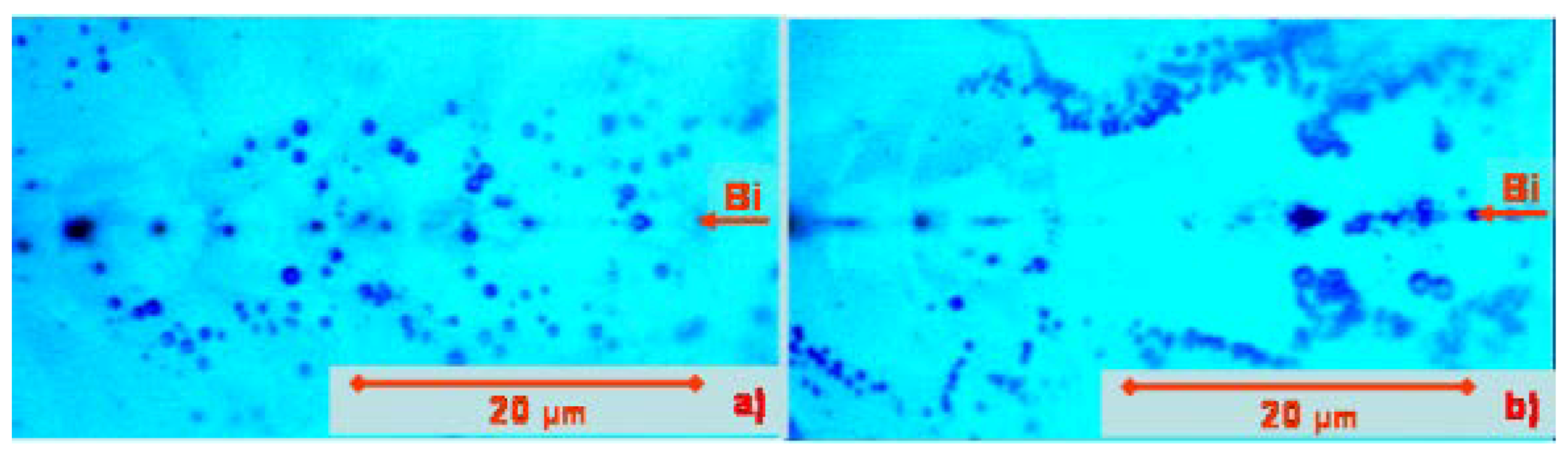
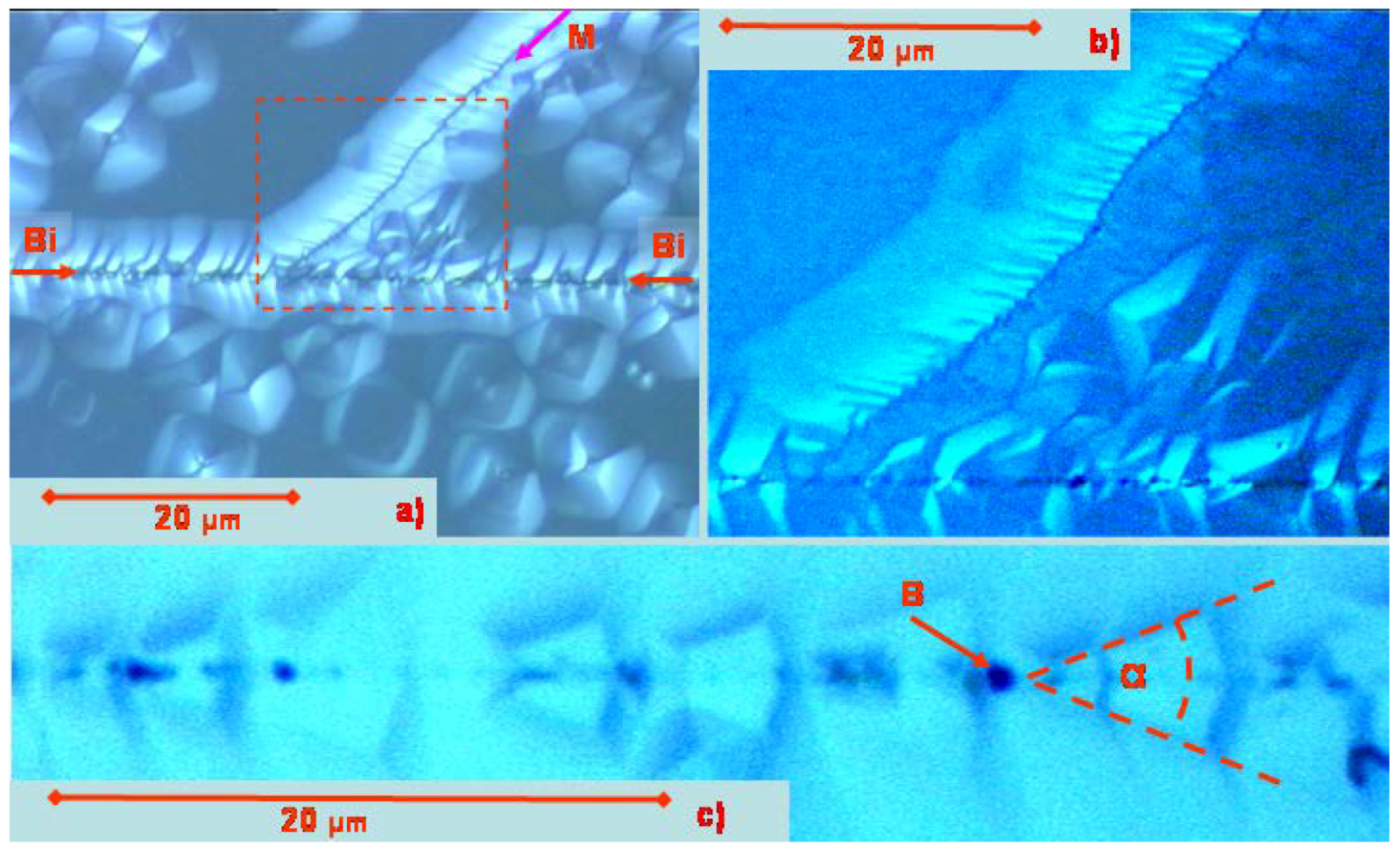
5.6. AFM STM Study on Dislocations in TiO2 and SrTiO3 Crystals with Atomic Resolution

SPM techniques allow studying the surface with atomic resolution [66,67]. These very sensitive techniques can be used for a precise analysis of the ordering of atoms close to the exit of dislocations in the plane of the surface. The lion’s share of AFM or STM studies with atomic resolution was obtained on surfaces which have been prepared via sputtering and subsequent thermal treatment. The STM or AFM pictures from such surfaces show a perfect reconstruction of the surface on the nanoscale and only a few numbers of point defects. Here it is worth emphasizing that there only very few AFM or STM measurements of dislocations exist in the literature with the highest resolution available [68,120].
Figure 31 presents the distributions of the atoms close to the cores of two partial dislocations.

6. Calculations of the Electronic Structure and Molecular Atomic Modelling of the Cores of Dislocations in TiO2 or SrTiO3 Crystals

6.1. DFT Calculation and Atomic Simulations

We have discussed above that in edge dislocations planes or half-planes terminate inside the perfect crystal lattice. In metallic systems, where the valence electron density is free-electron like, such extended defect will not drastically modify the electronic properties of the system while, of course, the mechanical properties will be affected. In the insulating oxide, where covalent or ionic bonding dominates, a terminated plane will necessarily exhibit dangling bonds or, if possible, a local reconstruction of the lattice with modified electronic properties.
To understand the basic mechanisms that appear when a defect is introduced in a crystal like SrTiO3 or TiO2, it is useful to look at point defects first. Density functional theory (DFT) [202] is a widely-used tool to study the electronic rearrangements in these materials, but care has to be taken when dealing with defects in oxides. Early calculations by Shanthi and Sarma [203] indicated that oxygen deficient SrTiO3 is in a metallic state as the defect levels overlap with the bottom of the conduction band of the oxide. This is caused by the underestimation of the band gap of most materials in DFT and later calculations using hybrid functionals found that these defect states are narrow and about 0.8 eV below the conduction band, as expected [204]. The situation is similar in TiO2 where oxygen vacancies (VO) create defect levels at an energy of 0.5 to 0.9 eV below the conduction band edge [205].
Using DFT it is also possible to calculate formation energies of single defects and these studies have been performed on different levels of the theory [206,207]. One has to keep in mind that the creation of a VO by removing ½ O2 leaves behind two electrons that localize on neighboring Ti atoms. In SrTiO3 these electrons occupy dz2-type orbitals oriented in the Ti-VO-Ti axis. It is well known that in 3d atoms in d1 configuration strong Coulomb interaction plays an important role and the occupancy of the levels (and their conducting properties) are determined by correlation effects [208]. Therefore, often the so-called DFT + U method is used, that incorporates additional correlation effects in an approximate scheme [209]. The dominance of localized, directed orbitals also affects the vacancy-vacancy interaction in these oxides. It is, therefore, not surprising that in some of these calculations a tendency of clustering of defects has been observed, both for SrTiO3 [210] and for TiO2 [211]. If a Ti atom is surrounded by two oxygen vacancies, e.g., in a Ti-VO-Ti-VO-Ti configuration, the middle atom is in d2 configuration and the second electron can occupy the conduction band of the oxide [210]. This induces a complex interplay between defect arrangement, charge state, and electronic properties.
In an extended defect, e.g., when a full plane of SrO is removed from SrTiO3, the resulting structure resembles an interface between two TiO2-terminated surfaces. At this interface, it is energetically favorable to displace the two sides by an ½ [010] translation. Such arrangements have been found in HAADF-STEM images of in low-angle tilt grain boundaries [74] discussed above.
In the same manner it is possible to remove a full TiO2 plane from the perovskite lattice and displace by an ½ [110] translation to arrange the SrO layers in a rocksalt like structure. Such SrO-SrO arrangements form under Sr rich conditions in a periodic arrangement giving rise to Ruddlesden-Popper (RP) phases. DFT calculations predict that these extra SrO layers are energetically easy to incorporate and do not affect the electronic properties of SrTiO3 significantly [212].
The situation is more complex if a half-plane (or, as in some calculations a one-dimensional ribbon) of SrO is removed from SrTiO3. In general, the electronic structure will depend on the boundary conditions of the removed part: if a ribbon is removed that is on one side oxygen- on the other strontium-terminated (Figure 32) the charge neutrality is retained; no defect states are created and only a reduction of the band-gap due to “internal surface-states” at the defect site is obtained. Due to the non-vanishing dipole moment of the removed part of the crystal, strong local distortions of the lattice accompany the defect. If the removed ribbon is Sr-terminated at both edges, defect states appear in the gap, again d electrons localized on the Ti atoms at the edges, that can form conduction channels [55]. In a more realistic model of the dislocation core [39] there will be more effects to consider, e.g., an off-stoichiometry around the defect and long-range relaxations that are difficult to model in general.
It was already mentioned that in TiO2 oxygen vacancies have a tendency to form linear arrangements [211]. In this arrangement, the Fermi level cuts the conduction band formed by Ti d states. Calculations show that the associated charge density decays exponentially with distance from the linear defect and is reduced by four orders of magnitude within a nanometer [48]. This behavior is in line with LC-AFM measurements of electrically active channels on a TiO2 surface. Also, other larger one-dimensional defect arrangements that show oxygen deficiencies have conductive states confined within a few nanometers.
Although several DFT studies were concerned with the structure and defect energetics of grain boundaries and dislocation cores, not much is reported on the electronic structure in these defects. Recent work on bicrystalline boundaries in SrTiO3 and TiO2 confirmed good agreement between the structures obtained in DFT calculations and observed in HAADF-STEM measurements. Calculations of the dislocation core as shown in Figure 1 show that the local inherent non-stoichiometry gives rise to spin-polarized states at the Fermi level that lead to a mixed +3/+4 valence state of the Ti atoms in the core [32]. Again, these states are rather confined (see Figure 33) and can serve as localized conduction channel.
Although the exact structure and electronic configuration at these extended defects is hard to capture (and probably in reality quite diverse) there are certain features that can be predicted by DFT calculations: Whenever electrons are localized in defect levels at the edges of dislocations or they will form states that are confined within a few nm around the defect. This behavior is very similar to the one observed in charged domain walls in perovskites, e.g., Pb(Ti,Zr)O3, where the structural distortions around the longitudinal domain wall are limited to a few unit cells [213]. Also in this case DFT + U calculations have shown that correlation effects have the tendency to localize Ti d electrons ensuring a rather sharp domain wall [214]. At least when 3d transition metal states are involved in the formation of the conduction band, this localization seems to be a general trend in oxides. Also at the (001) interface of LaAlO3 with SrTiO3 it was reported that the two-dimensional electron gas formed there is confined within a few nanometers [215].

6.2. Molecular Atomic Simulation

In recent years, atomistic simulations have become a versatile tool for the investigation of dislocations in SrTiO3 thanks to the enhanced computational power and the availability of supercomputers to the research community and a variety of simulations of the influence of dislocations on the structural behavior as well as on the ionic transport has been performed. In molecular dynamics simulations, the forces between the atoms within the simulation cell are calculated and the resulting positions of the atoms are determined in an iterative process. Using indentation in combination with etch-pit analysis the structure and evolution of dislocations under external loads were investigated and corresponding molecular dynamics simulations were conducted showing that the evolution of dislocations as consequence of a mechanical stress is strongly influenced by preexisting dislocations [113]. When a (001) oriented SrTiO3 crystal is plastically deformed by indentation, at first dislocation pile-ups are aligned in <100> directions while at higher loads an orientation in <110> directions is preferred revealing that the evolution and arrangement of the network of dislocations is related to a glide plane mechanism determined by the crystal structure. The simulations indicate that within the glide plane the dislocations tend to dissociate in two partial dislocations with distances of 4-5 nm separated by a strongly distorted antiphase boundary stacking fault [216]. The gliding of dislocations is also strongly temperature-dependent since it was calculated that at high temperatures the dislocations lose their mobility leading to brittle behavior of the crystal [105]. By employing a concurrent atomistic continuum simulation Yang et al. [95] also confirmed the importance of easy glide planes in SrTiO3 resulting in a preference of the <110> directions for dislocation nucleation and revealed that the presence of an agglomeration of dislocations in form of bicrystalline boundaries in SrTiO3 has a significant effect on the mechanical properties and the crack evolution [97]. Bicrystals have also been widely investigated in order to determine whether dislocations have an impact on the ionic transport of oxygen [45] or not [17]. By molecular dynamics simulations of dislocations it was found that the formation enthalpy of oxygen vacancies is significantly lower compared to the bulk [31]. Hence, in a non-equilibrium situation as is typically present during vacuum annealing, the dislocations will be reduced at first, accompanied by a local insulator-metal-transition resulting in the evolution of a network of conducting nanowires within a less-conductive matrix. On the other hand, it was calculated that in thermodynamic equilibrium the self-diffusion (tracer diffusion) of vacancies along the dislocation is suppressed [30] and Marrocchelli et al. [31] concluded that dislocations are “easy to reduce but not so fast for oxygen transport”.

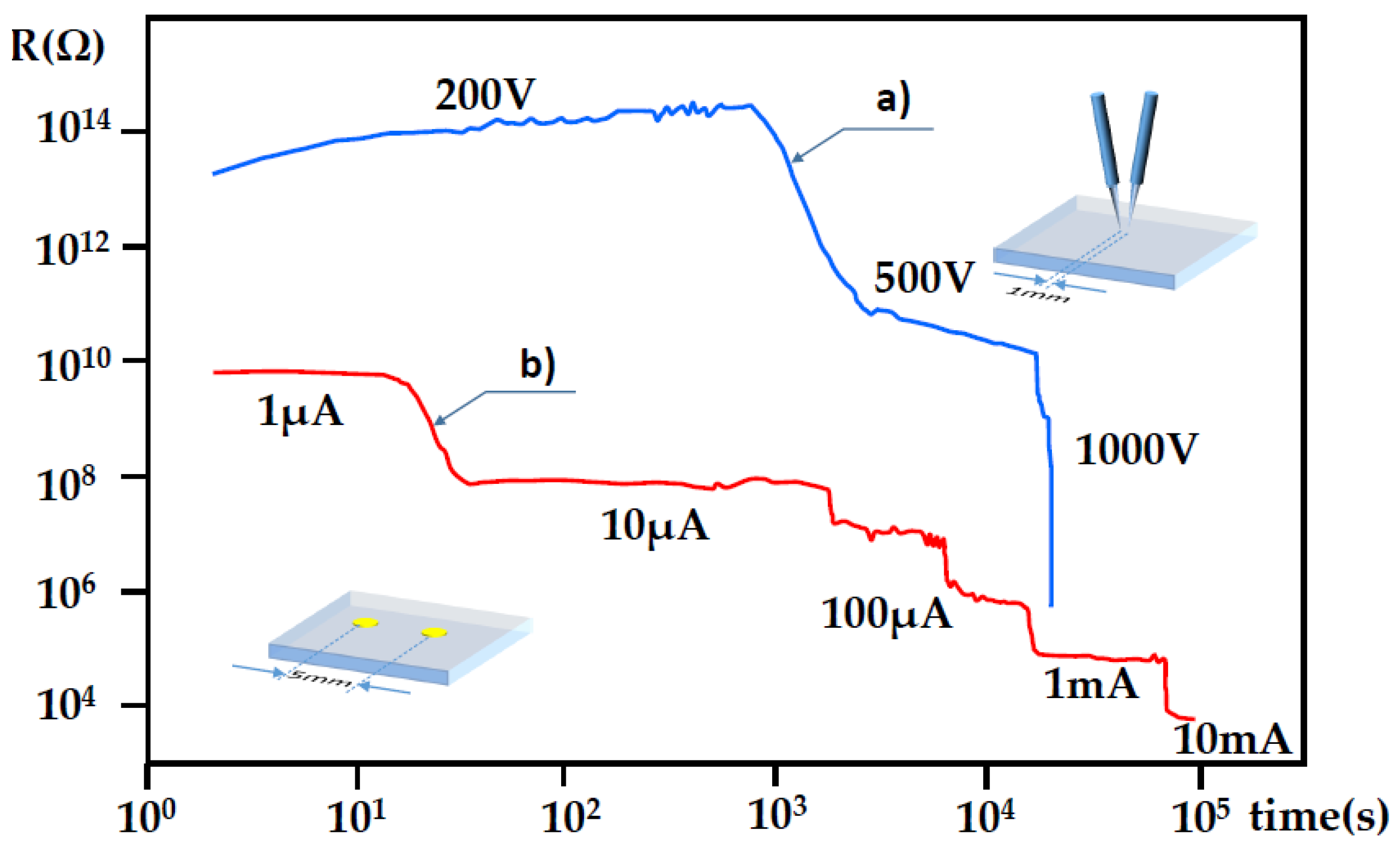
7. Electrical Properties of the Dislocations in TiO2 and SrTiO3

The crystallographic and electronic structure as well as the chemical composition of the core of dislocations in SrTiO3 and TiO2, as presented in subchapters 5.3.1 and 5.3.2, disclose the fundamentally different physical properties of these objects in the matrix of the two band insulators of our review. In contrast to dislocations in a metal, which show only small modifications in the electronic structure and can be regarded as neutral relative to the rest of the matrix from the electrical point of view (in the matrix we have a free electron gas), the electrical neutrality of non-metallic ionic or ionic-covalent oxides is not given. Before detailed microscopic data with atomic resolution were available, models about the electrical properties of the crystals with dislocations and especially the screening along dislocations (e.g., polycrystalline boundary) were proposed, for instance on the basis of impedance spectroscopy measurements or the analysis of electrical transport phenomena [30,217,218,219]. Already back in 1978, it was reported that the dislocations in the paraelectric phase of BaTiO3 single crystals are responsible for “an increased mobility of charge carriers” [220]. The high potential of ceramics on the basis of the transition metal oxides, such as BTO, PZT, BST, for applications in microelectronics has aroused great interest in the understanding of the influence of the polycrystalline boundary (especially the small angle boundary, which was associated in the literature with an array of dislocations with distribution in equidistance along the boundary line) on the global dielectric answer of the ceramic capacitor. Early models about the special role of the boundary in the ceramic materials or artificial bicrystalline boundaries, which have been obtained on the basis of the dielectric spectroscopic studies, have put in the foreground the screening phenomena close to the boundary (with dislocations). In their spirit, these models were a kind of direct adaptation of the space charge model known from semiconductor physics. It should be accepted that, on the basis of the data from impedance spectroscopy measurements of crystals with dislocations and ceramic grain boundaries, these models were a plausible and valuable approach for the description of the neutralization process of the surplus charge in the core of dislocations which can, e.g., agglomerate along a small angle and high angle crystalline boundary. Thanks to the knowledge from EELS spectroscopy about the local valence of the transition metal ions along the core of edge dislocations in TiO2 and SrTiO3 (see above), the existence of a high concentration of Ti3+ or Ti2+ ions in the core of edge dislocations became evident in both materials, and new data from the electron-holographic investigations, considering the charging of the core of dislocations (e.g.,: [11,12,30,40]), started a broad discussion about how the “impedance spectroscopic” description and the “atomic” models (which are directly extracted from TEM-based techniques) could be correlated. The best illustration of the discrepancies encountered for these two perspectives was presented in the paper by Alfthan et al. [92]. The authors proofed, on the one hand, the validity of the classical space charge model by impedance spectroscopy measurements but demonstrated, on the other hand, by use of electron holographic measurements that the core of dislocations has an opposite polarity (here a negative charging of the core of the dislocations) relatively to the mentioned impedance models. However, the discrepancy in this work was connected with an estimation of the spreading of the potential profile (from impedance studies) of about 30 nm (at the grain boundary; here the bicrystalline boundary) with respect to a direct measurement of the dimension of the potential profile of the negatively charged core of single dislocation (by electron holography) resulting in ~2 nm. Note: such holographic results could be considered as a direct projection of the potential distribution in the core of dislocations (~2 nm) [221]. The difference in the extension of the space charge zone presented by Alfthan et al. [91] is here just 2 nm to 30 nm, but measurements of the surface potential distribution, which have been obtained for a similar system (here bicrystalline SrTiO3) using non-contact KPM by Kalinin et al. [94], even indicated that the dimension of the space charge region may be as large as 1.5 μm.
Instead of discussing how the electrical properties of isolated dislocations and their contribution can be “extracted” from the global electric or “dielectric answer” in a real crystal, we should focus our attention at this point of our review on the possibility of investigating individual dislocations under different electrical or mechanical stress.
If we accept that the core of dislocations possesses the typical characteristics of low titanium oxides (including a high concentration of d1 or d2 delocalized electrons) and that the Burgers vector of dislocations is invariant (i.e., dislocations cannot simply end within the crystal but only on the outer or an inner surface or by crossing another dislocation) we should observe an inhomogeneity in the distribution of the electrical conductivity in plane of the surface using modern LCAFM studies. The advantage of the LCAFM technique is connected with the very small contact area between the apex of the conducting tip of the cantilever and the investigated surface, which in fact determines 90% of the potential drop and thereby contributes in similar scale to the spreading resistance. The real mechanical contact area of the tip and the galvanic contact area are not the same, which can be simply proofed using Fowler-Nordheim tunneling through very thin SiO2 films [222]. It is surprising that for the tip with typical radius 10 nm the electrical contact can be reduced to only ~1 nm2. Therefore, it is possible to analyze using LCAFM the map of the electrical conductivity with atomic resolution. Notice: for the correctly prepared surface (after removal of the physisorbates and chemisorbates) of a homogenously conducting material the uniformity of the electrical conductivity is indeed measureable by LCAFM in the plane of the scanned surface (e.g., Au thin films [223]). Other test measurements, here of highly oriented pyrolytic graphite HOPG, reveal small but regular modulations of conductivity on an atomic scale related to its crystallographic structure. Turning to the analysis of the electrical conductivity of the oxides (here band insulators) on the nano-scale poses a further challenge, in that measurements have to be conducted at extremal low values of currents down to 10−12–10−15 A. Facilitating such measurements at ultra-low conductivity does require a very sensitive LCAFM current-to-voltage converter (with reduced parasitic capacity in feedback of the I/V converter [224]), see Figure 34).
Spatial variations of the electrical conductivity of stoichiometric crystalline oxides have been observed by LCAFM on the surface of a number of binary and ternary band insulators. This includes our oxides of choice in this review: TiO2 [48,53], SrTiO3 crystals [50,51,55,68,225,226], and doped SrTiO3 such as Nb:SrTiO3 [227], La:SrTiO3 [228], Fe:SrTiO3 [58], as well as related oxides such as BaTiO3 [229,230], PbZrO3 [231], KTaO3 [232], NaNbO3 [233,234], and BiFeO3 [235]. Similar effects have also been observed for thin films, see, e.g., TiO2 [236], SrTiO3, Fe:SrTiO3 [225,237,238,239], BaTiO3 [230,240], HfO2 [241,242,243,244], and NiO [245]. Here, examples of the current (resistance) mapping of SrTiO3 and TiO2 are given in Figure 35 and Figure 36, respectively. It should also be noticed that TEM images of SrTiO3:Nb give a rather homogeneous picture of the samples [246], while LCAFM measurements indicate spatial fluctuations of the conductivity at the surface [227].
Of course, the observation of a local variation of the current by LCAFM studies in the surface plane of the stoichiometric crystals does not necessarily imply that the dislocations play an important role in the electrical transport. Although the measurements were obtained under vacuum condition and after thermal desorption of water (at 250 °C), one should take into account that the rest of the physisorbates or chemisorbates can still exert an influence on the local potential distribution and may automatically modify the local conductivity [230]. A clear evidence for the role of dislocations stems from LCAFM analysis of regions with high concentration of dislocations which have been artificially induced, for example, along steps in a plastically deformed crystal (Figure 37) or at a bicrystalline boundary (Figure 38). Here, the current (or resistance) maps show unequivocally a correlation between the position of conducting filaments and the locations of dislocations. From these data, one can extract that the electrical conductivity of the dislocations for stoichiometric SrTiO3 and TiO2 is at least of 2–3 order of magnitude higher than the conductivity of the matrix. However, it is not possible to precisely determine the actual electrical resistance of the matrix due to the finite current sensitivity of the I/V converter in use (see Figure 35, Figure 37 and Figure 38). Therefore, one can only state at this point that the local resistance is higher than 1 PΩ (Peta Ohm).
An additional thermal reduction of the crystal enhances the concentration of the oxygen vacancies [48,50,51,53,55,68,222,225,226] along the dislocations, which in turn leads to a further local increase of the electrical conductivity (with dominance of the electronic conductivity). In contrast to the electrical conductivity of dislocations in stoichiometric crystals, LCAFM studies of reduced crystal do indeed show an enhancement of the conductivity of the core of dislocations relative to the surrounding matrix, leading now to values higher than 3–6 orders of magnitude with respect to the background (here notice also from an experimental point of view that the dynamic of the LCAFM measurements can be increased by a parallel investigation of the regions between dislocations using a higher sensitivity of the I/V converter). This gives an added opportunity to correlate the position of the conducting filaments and the core of dislocations by LCAFM investigations for reduced SrTiO3 [51], reduced bi-crystalline SrTiO3 and TiO2 crystals [48]. For this, pre-etched crystals were investigated after thermal reduction under vacuum conditions, showing that the position of filaments is localized at the center of etch pits which mark the position where the dislocation line crosses the surface (Figure 39, Figure 40 and Figure 41).
So far, LCAFM was only used to map the electrical conductivity of the surface. In order to analyze the electrical conductivity below the surface in an out-of-plane direction, one can additionally cleave the crystals to obtain cross-sectional LCAFM maps.
The fold-up maps of the conductivity in-plane and out-of-plane indicate that a 3D network of filaments exists whose structure is a hierarchical network with high density of the extended defects very close to the surface and a declining concentration of defects in deeper parts of the surface region. A prominent example of such a hierarchical structure with locally enhanced conductivity is presented for a TiO2 single crystal (see Figure 42) which was subjected to a thermal reduction strong enough to establish a pronounced, well-structured network of filaments (here, probably due to a chemical restructuring of the dislocation cores) [48]. We have found a similar density distribution of filaments in the surface region of reduced SrTiO3 crystals (see Figure 43) with a high concentration of well-conducting filaments near the surface and a decline of the density towards the interior of the reduced crystal. Notice: to avoid the interaction with rest gases cleaving of the crystals was undertaken in situ under very low oxygen partial pressure (here 10 mbar of H2).
All our results indicate that the hierarchical structure of conducting filaments (Figure 42 and Figure 43) shows similarities to the distribution of the density of dislocations as obtained from electron microscopy (see [10,42]). We are aware that we have generated new populations of dislocations during cleaving our samples for the LCAFM studies of the out-of-plane distribution of conducting filaments in reduced SrTiO3 or TiO2. However, their conductivity is equivalent to the very low conductivity of dislocations in the crystals without additional reduction. This in turn implies that the “electrical traces” of such mechanically created, new dislocations are invisible for the typical dynamical range of LCAFM measurements for reduced crystals (with current resolution of 4 orders of magnitude). It is important to emphasize that the “electrical trace” of the hierarchical structure in the surface region does not show a noticeable influence of the cleaving conditions for both reduced materials (in situ under vacuum or in H2, as well as ex situ). The most important effect is the preferential reduction of the core of dislocations [31], and “cylindrical distribution of oxygen vacancies around dislocation lines in the crystal” [247]. For a such cylindrical Cottrell atmosphere (with a typical radius between 1 to 10 nm) we can estimate (after determination of the total concentration of the removed oxygen during reduction; see Figure 44) the local concentration of d1 electrons of strongly reduced SrTiO3 and TiO2 crystals be in the order of 1020–1022 /cm3 (see, e.g., [45]). Notice: the EELS measurement of the core of dislocations for stoichiometric crystal shows that the original concentration of d electrons is a few percent, which is in fact very high close to the metallic limit [39,40,94]. Thus, the enormous additional doping by reduction (or preferential self-doping induced by removing of oxygen from the core of dislocations) is in our opinion connected with a delocalization of the high concentration of d1 electrons along such extended defects in a pre-existing network (caused by the invariance of the Burgers vectors) and could be made responsible for the insulator-to-metal transition in reduced SrTiO3 [55] and TiO2 crystals [53]. Notice: we have already mentioned above that Buban et al. [40] have clearly presented, using EELS measurement, that the dislocations in SrTiO3 can be associated with TiO nanowires and R. Sun et al. [32] have made a similar statement about the role of the core of dislocations in TiO2 as conducting nano-wires. The insulator-to-metal transition is a long-standing problem in the literature and is often associated with the famous Mott criterion [248] which connects the stability of the metallic state with the carrier concentration (n) and the effective Bohr radius (aH) of an electron-hole pair, where a H = ε m e 2 (Equation (1)). The critical concentration of the carriers can be calculated from the formula n 1 / 3 × a H = 0.2   ( 0.254 ) (Equation (2)). The Mott criterion is not only valid for doped semiconductors but also for transition metal oxides. Cox in his book [203] has pointed out that the critical concentration of the electrons for the insulator-to-metal transition in SrTiO3 crystal should be of order of 4.1 × 1018 cm3 (the calculations were obtained using Equation (1), for ɛ = 300 (at RT), and m* = 10 m0 (see, e.g., [249]) as well as the collection of data in [250]). In the meantime, an upper bound of the critical concentration was even estimated to be as low as 1016/cm3 based on electrical measurements [251]. If we neglect for the time being the idea that the d1 electrons are selectively agglomerated along dislocation lines and are responsible for the local insulator-to-metal transition and postulate instead that the oxygen vacancies are distributed statistically in the reduced crystal we can calculate an effective Bohr radius aH for the electron carriers. Using in our case 1015/cm3 as obtained from the above-mentioned effusion measurements, we can determine the Bohr radius according to Equation (2) to be around 26 nm. Since the Bohr radius is connected with the dielectric constant and the effective mass via Equation (1), we can then estimate using these numbers that the dielectric constant has to be ε = 4000 when the effective mass, as specified in literature, is ~10 m0 (a maximal value). However, this overestimates the dielectric constant of SrTiO3 at RT by one order of magnitude. On the other hand, Spinelli et al. [251] estimated values for aH of 200 nm at RT and as large as 10 μm for low temperatures, where ɛ is enhanced by two orders of magnitude. To cope with the very low value of the carrier concentration limit in the case of the classical interpretation of the insulator-to-metal transition for SrTiO3 other authors have suggested resolving the contradiction by applying, e.g., the Mott–Ioffe–Regel (MIR) limit [252]. This model can be used when the mean-free-path of a carrier falls below its Fermi wavelength or the length is smaller than the lattice constant (interatomic distance). Thus, in the literature values of aH ranging from 1 nm [253] to several micrometers can be found.
This brings us back to the dislocations and their role for an understanding of the nanoscopic nature of insulator-to-metal transition. Maybe a simple experiment provides convincing arguments for the important role of the dislocations by considering two pieces from the same substrate with different density of dislocations and exposing them simultaneously to the same reduction conditions. For this, we used one piece with a high concentration of dislocations, here around 1012/cm2 in the surface region, which was generated by mechanical polishing, and another piece with the original epi-polished surface (here the concentration of dislocations is of order 1010/cm2). These two samples were simultaneously reduced to the minimum of the resistance of the bathtub curve (see, e.g., [45,226]) and subsequently cooled down to room temperature. Under these conditions, the electrical measurements revealed that the temperature dependence of the resistance for the crystal with high concentration of dislocations is typical for a metallic behavior while it exhibits only semiconducting behavior in the case of the epi-polished crystal (see Figure 45). This does not necessarily imply that individual dislocations in the latter (semiconducting) case may not turn metallic in character but their contribution is simply not sufficient to produce an overall (macroscopic) metallic behavior. It should be noted that the probability of a bundling of dislocations is higher for crystals with high density than for the crystal with low density of dislocations (see, e.g., above in the case of bicrystalline boundaries in Figure 37, Figure 38 and Figure 41). As an effect, such bundles may result in a higher degree of oxygen nonstoichiometry and may, therefore, be more easily transformed to become metallic in character. The simple experiment is also a fine illustration that further systematic and quantitative studies are necessary to compare nanoscopic and macroscopic measurements and to take the inhomogeneity of the crystalline material and the surface region into account.
A further support for the notion of the inhomogeneity of the electrical conductivity in SrTiO3 crystals and the important contribution from the core of dislocations stems from Electron Beam Induced Current (EBIC) studies on reduced SrTiO3 crystals. Using appropriate Schottky contacts (in this case, a thin Pt electrode becomes deposited on the surface of reduced SrTiO3 crystal [241,242]) the contributions of different locations in the surface region (i.e., below the contact) for recombination processes of the incident electron beam can be analyzed. Measurement of the current at the bottom electrode synchronously to the scanning position of the incident electron (SEM) beam gives then the planar distribution of electronically active defects in the form of a current contrast. The EBIC maps for a reduced SrTiO3 crystal with a Pt/Schottky contact reveals an orthogonal arrangement of dislocations and two kinds of reactions to the electron irradiation (Figure 46). On the one hand, linear objects with reduced contrast (it corresponds probably to the electron interaction with dislocations with lower conductivity than the rest of the matrix) can be observed. On the other hand, dislocations with higher conductivity than the rest of the crystal can be identified by a higher EBIC contrast. This result is not surprising considering that two types of dislocations (Sr-rich and Ti-rich) exist in stoichiometric and reduced SrTiO3. The local electronic and crystallographic structure of these types of dislocation does indeed show dramatic differences. Similar EBIC investigation of the contact Pt/Nb:SrTiO3 (with Nb concentration of 0.01 weight percent) demonstrates that, even in a system with metallic conductivity, one can identify the bright contrast of a relatively high population of dislocations in the interface at an appropriate voltage, here V < 5 kV [13]. This implies that dislocations in such a system may even show an enhancement of the electrical activity though the surrounding crystalline structure is expected to be metallic in character.
The open question for LCAFM and EBIC investigations, here especially for donator doped crystals, is the influence of the surface layer. On the one hand, we know that the bulk of the Nb:SrTiO3 crystals possess a homogenous distribution of aliovalent Nb ions and, without doubt, the dislocations play only a minor role for the global metallic conductivity of the matrix induced by such chemical doping, as presented by Rodenbücher et al. [246]. On the other hand, in situ and in operando investigations using surface sensitive techniques of the surface layer of Nb:SrTiO3 [227] give evidence that the stoichiometry of Ti and Sr can dramatically change and the typical so-called metallic pick at the bottom of the conducting band actually disappears, which in turn “switches” the electrical properties of the surface region to become semiconducting in character. Therefore, a higher electrical activity of the dislocations can be observed in the surface region.
In essence, studies of the local conductivity of oxide surfaces, here summarized for the surface layer of SrTiO3 and TiO2, show that the presence of dislocations can lead to modifications of the electrical transport on the nano- and micro-scale. This effect could be connected with the frequently observed inhomogeneity of the electrical surface properties of oxide materials.

8. Role of Dislocations in Resistive Switching of TiO2 and SrTiO3 Crystals

Easy and preferential reduction of the dislocations cores in oxides cannot only be induced by thermal reduction at high temperatures and low oxygen partial pressures [45,51,55]. Another way to switch dislocations in both materials from being semiconducting (corresponding with their original state in the stoichiometric crystal) to become metallic filaments is possible using electrical polarization with appropriate voltage and current. Although it was already presented in 1962 that under external electrical stimuli the resistance of polycrystalline BaTiO3 can be reduced [254], only as recently as 1992 it was observed for KNbO3 that the resistance of single crystals can be easily increased by many orders of magnitude up to metallic behavior by the application of a constant voltage or constant current polarization [59]. As an effect, a dense set of filaments are being created between the position of the geometrical position of the cathode and a progressing virtual cathode. As a result of the electrical stimulus, the electrical conductivity of the whole crystal gets “switched” from insulating to metallic or even superconducting behavior [4] (see Figure 47 and Figure 48). Such transformation, i.e., switching, of the macroscopic crystal into an object with metallic conductivity (see the typical dependence of the resistance as a temperature function, Figure 47 or Figure 49), has been observed for many crystals with perovskite structure (SrTiO3 [45,51,55,68,225,226,255], see also Figure 49), Nb:SrTiO3 [227], Fe:SrTiO3 [58] (see also Figure 50 and Figure 51), La:SrTiO3 [228,256], BaTiO3 [257], KTaO3 [232], NaNbO3 [233,234], PbZrO3 [231], BiFeO3 [235], and binary crystals such as TiO2 [48,53] (see also Figure 52 and Figure 53). The electrically induced insulator-to-metal transformation is in its character very similar to the above described thermal reduction process (see previous chapter). The dynamics of the electrically induced change of the resistance for these ternary and binary crystals, relatively to the resistance of the stoichiometric crystal at room temperature, is highly effective and can be as large as 6 to 11 orders of magnitude.
The electrodegradation process is accompanied by two visual effects: on the one hand, one observes a modification of the color due to a network of bands with better electrical conductivity compared to the rest of the crystal (often the bands possess an orthogonal orientation, see Figure 54 and Figure 55). On the other hand, bubbles develop on the metal film of the anode in the course of the electrical stimulus. Even more, the bubbles do not disappear after switching “off” of the electrical polarization. The bubbles decorate the positions on the anode at which oxygen ions or molecules leave the crystal (see Figure 56). Because the electrodes are in principle obtained from a hermetic material (here, thin uniform deposited metallic films, e.g., Pt or Au) the effusion of the oxygen into the surroundings is hindered. After having reached a critical pressure, this causes a local plastic deformation of the electrode [48,51,53,55,58] (see Figure 54, Figure 55 and Figure 56). A similar electrodegradation process undertaken for the system Pt/SrTiO3/Pt with porous electrodes shows that the system is in fact open and effusion of oxygen becomes detectable. The effusion of oxygen from the crystals can be monitored by mass spectroscopy in the course of the electrodegradation processes. The thus measured, electrically induced increase of the oxygen nonstoichiometry in the SrTiO3 crystal is of the order of 1015/cm3 (for 1 mA) or 1016/cm3 (for 10 mA) (see Figure 57) and is thus one or two orders of magnitude higher than for thermal reduction, respectively (see Figure 44). Therefore, it should not be surprising that the system for this electrically enforced oxygen nonstoichiometry has been switched into the metallic state (Figure 49). At this point it is interesting to raise the question whether the nature of the electrical insulator-to-metal transition is similar to the processes involved in thermal treatment; here in particular considering the aspect whether the electrically induced removal of oxygen is limited to the core of dislocations in the surface layer of SrTiO3 or TiO2. The first indicator that this assertion may be true is the fact that there exists a correlation between the arrangement of the bubbles and the crystallographic direction of the material, which can easily be checked using simple optical microscopic inspection (see, e.g., Figure 54, Figure 55 and Figure 56). Another convincing argument for this hypothesis is the observation of bubbles evolving along the bicrystalline boundary (see Figure 56).
A further, though indirect, effect which suggests the important role of dislocations in the electrodegradation phenomena is related to the easy chemical transformations of the cathode region of, e.g., TiO2 crystal into Magnéli phases, as confirmed by X-ray and electrical measurement [53]. The argument is, that, following Landuyt, and Amelickx [124,258], dislocations (so-called hairpin dislocations) are a necessary requisite for this kind of solid state reaction to occur.
A participation of an array of dislocations or their bundles (agglomerated along a bicrystalline boundary) can not only be identified for electro-migration processes, but the self-diffusion of oxygen in bicrystalline SrTiO3 at high temperatures is similar in character. An illustration of a selective incorporation of 18O isotope (under equilibrium condition) is given in Figure 58, where the exchange of isotopes takes place preferentially along the boundary as well as in regions with a high concentration of dislocations originating from local mechanical damage [259].
The insulator-to-metal transition induced by electrodegradation cannot only be studied on the macroscopic scale using two or four-point electrical measurement or optical inspection, but also the nanoscopic dimension of this transformation can again be investigated using LCAFM techniques. As illustrated in Figure 59, Figure 60 and Figure 61, one can clearly discern a fine structure of conducting filaments along bands between the cathode and the anode on the surface of electro-reduced crystals (here SrTiO3, Fe SrTiO3, TiO2) with a planar geometry of the electrodes. This linear arrangement indicates a correlation between the position of the filaments and the position of dislocations or dislocations bands. Moreover, etch pits investigation on such electrodegraded crystals support this notion in that the etch pits accumulate in just the same way along the bands with high concentration of filaments. It should be mentioned that the local enhancement of the conductivity of filaments with respect to the matrix amounts to three to four orders of magnitude.
Additional supporting argument about the important role of dislocations in the electric activity of the surface layer of SrTiO3 can be obtained from the analysis of the already above mentioned EBIC measurements for stoichiometric [242] (see also Figure 46) and as well as for doped SrTiO3 crystals [241]. One can see that the brightness of the EBIC contrast in the vicinity of the straight lines which marking the segments of dislocations can be changed by applying a bias voltage in the case of undoped SrTiO3 crystals (here −10 V, Figure 62) and Nb-doped SrTiO3 (0.01%) (−2 V, Figure 63), respectively.
An important aspect of the foregoing analysis is the possibility to locate and electrically address individual dislocations crossing the surface, as demonstrated in the case of SrTiO3 [51,55,68,225,260] and TiO2 [48,53]. In fact, LCAFM has proved to be an invaluable tool for this, as it allows us to address single dislocations crossing the surface with adequate spatial resolution, and use, at the same time, the conducting cantilever as a nanoelectrode through galvanic point contact. Some preparatory procedures by brief thermal pre-treatment allowed to easily locate single dislocations with radius of about 2 nm and then influence and modulate the electrical state with currents smaller than 1 μA [68] (Figure 64). Due to the low current necessary, the process cannot be classified as only a thermally stimulated process (e.g., [261]). In our scenario of the resistive switching of individual dislocations in SrTiO3 via the conducting tip of the LCAFM cantilever the following parameters play an important role:
  • the polarization (negative or positive) of the tip,
  • the voltage, i.e., local strength of the electrical field, and
  • the low oxygen partial pressure available in the AFM microscope.
For the negatively polarized tip of the cantilever it is possible to reduce the concentration of oxygen in the last segment of the dislocations crossing the surface by a cathode attack of hot electrons which will be emitted via field emission from the tip [55,68]. This way, the dislocations can be reduced successively on the full length by the movement of the “virtual cathode”. This electrical state can be defined as a low resistance state (LRS) (Figure 64a–c). DFT analysis demonstrates that an increase of the oxygen non-stoichiometry along a dislocation core induces a metallic state close to the bottom of the conductions band. For the opposite polarization of the LCAFM tip (here positive), oxygen ions can be pulled from the inner network of dislocations and moved to those parts of the dislocations which contain a high concentration of oxygen vacancies. This then resembles an oxidation process of the core of dislocations which leads to an “annihilation” of the metallic state in the band gap. (This oxidation process restores the original semiconducting properties of the core of dislocations, the so-called high resistance state (HRS)). Also, on the TiO2 surface, highly localized regions such as conducting grains with diameters of several tens of nanometers can be switched between states of different conductivity [53] (see Figure 65).
This effect of a “preferential addressing” of dislocations during electrical polarization can be highlighted by inspecting the case of a bicrystalline boundary which is macroscopically electrodegraded employing a planar geometry of the electrodes (Figure 66a). After the electrodegradation, the local conductivity between the electrodes was measured by LCAFM under ultra-high vacuum (UHV) conditions. Although a broad area of the crystal was electrically polarized, a dramatic change of the electrical properties was only identifiable (on the micro- and nano-scale) along the bicrystalline boundary (Figure 66c). The nature of electroformation and switching along nano-filaments in single crystals is still under discussion [29,47,48,49,50,51,52,53,54,55,262,263]. One issue, which has not been dealt with in this chapter, is related to the possibility of a local transformation of the model binary and ternary oxides (here TiO2 and SrTiO3 crystal or thin films) into new chemical phases [e.g., Ti4O7, Ti5O9, Ti2O3, TiO, SrO·SrTiO3, or Sr2Ti6O13 or Sr1Ti11O20, [57,121,182,264,265,266,267]) under electrical stimuli. Such solid-state transformations are most likely connected with extended defects. This holds particularly true for dislocation cores which can be considered as foreign objects in the matrix (see above and [94]) due to their different crystallographic structure and chemical properties with respect to the surrounding matrix. They could thus play an important role as a “seed” for the thermally or electrically induced transformation. In fact, thermodynamic arguments show [268] that if the resistive switching would only be induced by a change of the center of gravity of the population of point defects in the crystal the induced, new resistance state would not be stable on a long time scale. We therefore argue that the chemical and crystallographic transformation of the core of dislocations seems to be a plausible alternative to models which solely rely on a Schottky-type disorder [267,269,270].

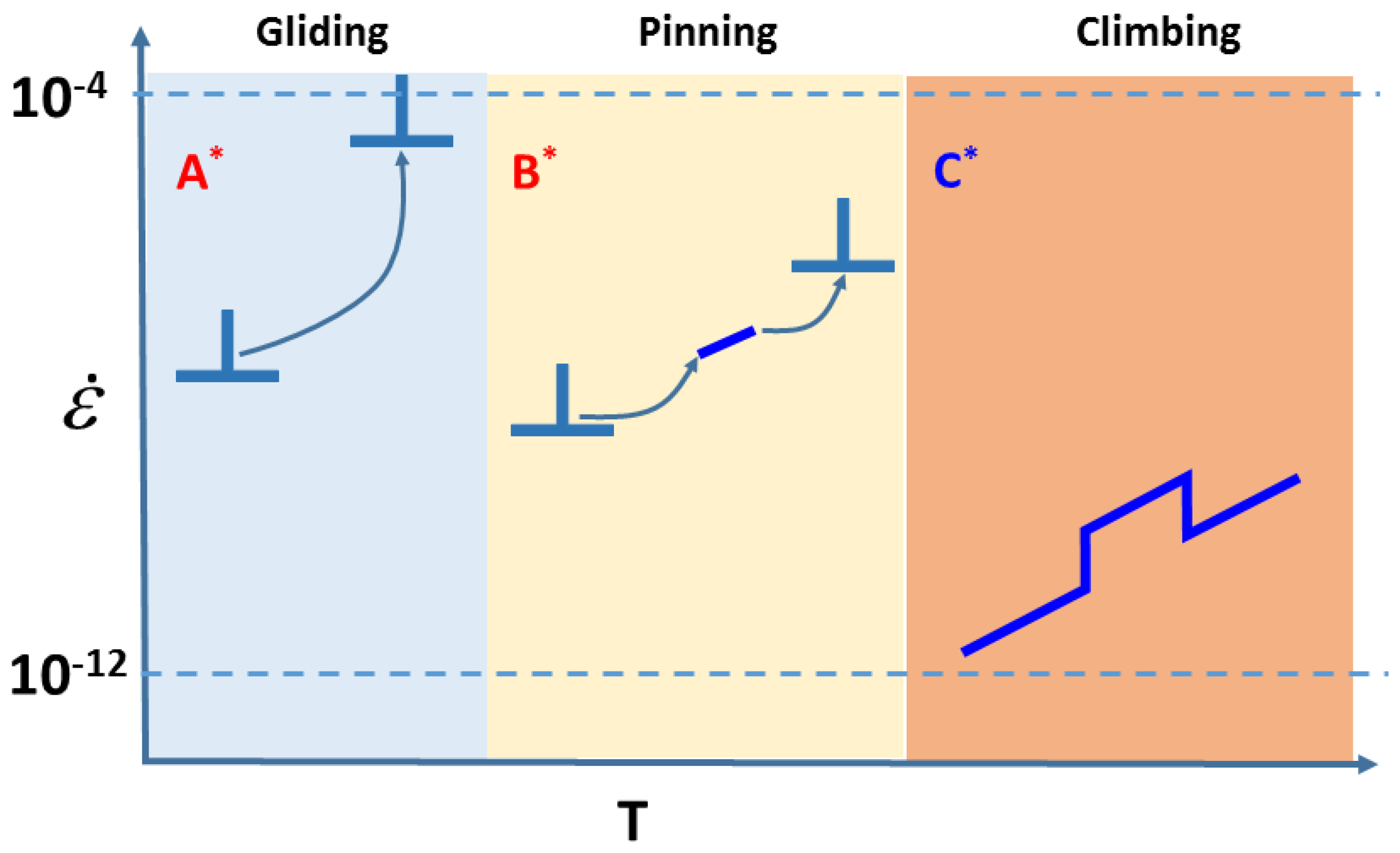
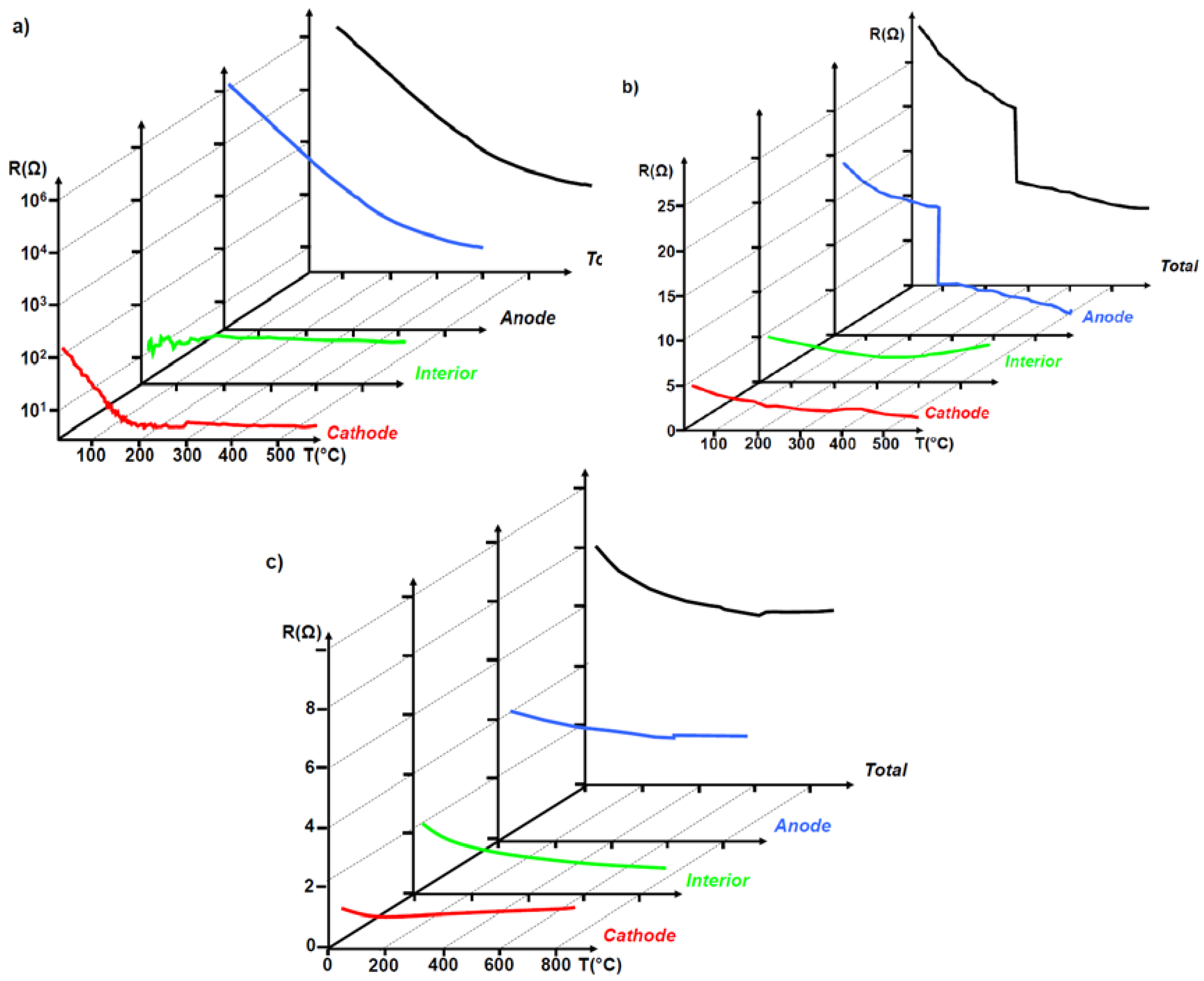
9. Mechanical Properties versus Dislocations

It may sound unrealistic if someone says that he can plastically deform a single SrTiO3 crystal with bare hands, but, as already mentioned above, this statement is indeed true. In fact, the ductility of the SrTiO3 crystal at room temperature is just about 10% [68,107]. Using the device which is illustrated in Figure 67 it is possible to deform (plastically) a SrTiO3 crystal in a controlled manner [68,104,132]. Depending on the radius of the prism and external forces F1 and F2, the density of the steps and their height close to the contact lines (bands) can be manipulated (see Figure 67). This effect of an extraordinary shift of whole blocks of the crystal is connected with the polygonization of the edge dislocations in the plane {100} and {110}. An impressive confirmation that the ductility of the mechanically deformed SrTiO3 crystal is connected with the linear arrangement of dislocations is given by the perfect ordering of the etch pits observed along the steps (Figure 68d–f). It should be mentioned that by mechanical deformation two different mechanism for the new ordering of dislocations become activated. The first one is connected with a shifting of the dislocations (via gliding) which exist in original crystal to new positions and their grouping in the appropriate gliding plane. The second mechanism has two steps. During the first step the new population of dislocations will be nucleated and subsequently, in the next step, the dislocations will be polygonized. The possibility to generate new dislocations is in fact an effect of the increase of the local pressure along the contact line (Figure 67) to values which allow their multiplication. Therefore, the density of the dislocations along the contact bands is much higher than the density of dislocations in the original crystal.
The plastic deformation of SrTiO3 crystals seems to takes place in principle along the <110>directions [15,16,33]. In our investigation with the mentioned configuration of the acting forces as presented in Figure 67, we found that the dislocations occasionally assemble in an arrangement along <110> while numerous groups of dislocations were observed with orientation in the direction <100> (see Figure 69a). At the same time, a crossing of these different directional arrangements can be observed and seems to be “independent”, that means without mutual interaction of both planes with accumulated dislocations (Figure 69b,c).

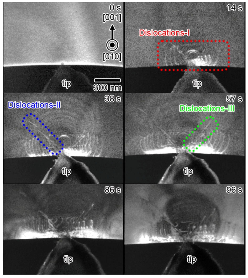
10. Dynamic Behavior of Dislocations in SrTiO3 by In Situ Nanoindentation Experiments inside TEM

In recent years, in situ observation techniques for transmission electron microscopy (TEM) have been developed for directly observing dynamic dislocation motions in crystals under stresses [271,272,273]. Especially, in situ TEM nanoindentation techniques [108,273,274,275,276] now allow us to dynamically observe dislocation behavior at an arbitrary local area in a TEM specimen even at nanometer dimensions. Moreover, if we use well-controlled bicrystals for TEM specimens, it should be possible to directly observe the interaction processes of dislocations with a well-defined grain boundary during deformation. In the present study, we use the in situ TEM nanoindentation technique to directly and dynamically observe the nanoscale deformation processes of SrTiO3 at room temperature. By using the suitable dark-field imaging conditions, we clearly highlight the dynamic behaviors of individual dislocations such as nucleation, propagation and interactions with other defects during the nanoindentation experiments [108,276].
First, we show the results of in situ TEM nanoindentation experiments of single crystalline SrTiO3 [108]. Figure 70a gives an overview of the in situ TEM nanoindentation system. We used a TEM-NanoIndenter holder (Nanofactory Instrument AB.) with a double-tilt capability as schematically shown in Figure 70b. The specimen motions can be precisely controlled by a piezo actuator and the specimen is gradually moved toward the fixed indenter tip as the nanoindentation proceeds. Here, a wedge-shaped diamond indenter tip was selected. Figure 70c shows the dark-field TEM image (using g = 002) of the specimen edge and the indenter tip just before the nanoindentation experiments. Then, the indenter tip was manually inserted along the [001] direction. Figure 71 shows the sequential dark-field TEM images captured from the movie recorded during the nanoindentation experiment. The complete movie is available elsewhere [108]. In the figure, 0 s corresponds to the moment when the indenter tip has just contacted with the SrTiO3 specimen edge. The indenter tip was gradually inserted into the specimen during 0 s to 65 s, and then extracted from the specimen during 65 s to 97 s. Here, we inserted the tip into a relatively thick specimen region in order to minimize the thin TEM specimen effects. It is noted that dislocations were generated from the specimen edge where the indenter tip contacted. The introduced dislocations may be classified into three different types, type-I, -II and -III dislocations. The type-I dislocations initially propagated in a semicircle shape, and then the dislocations split into two segments. This indicates that a part of the dislocation line reached to the specimen surface, leaving two dislocation segments. Then, each dislocation segment moved toward the ±[100] directions. The type-II and type-III dislocations were also nucleated near the indented area, but they moved toward the [101] and [ 1 ¯ 01] directions, respectively. In order to characterize the slip systems of the introduced dislocations, the static TEM analyses after the TEM nanoindentation experiment were carried out. The Burgers vectors were determined by the conventional g∙b = 0 invisibility criterion [277], and the slip planes were determined by the observations from the different crystallographic orientations. After the careful image contrast analyses, we found that there are two types of dislocation characters in the type-I dislocations: one is near-screw type dislocation with the slip system of [011](0 1 ¯ 1) type, while the other is also near-screw type dislocation but with the slip system of [0 1 ¯ 1](011) type. The type-II and type-III dislocations belong to the different slip systems of [101]( 1 ¯ 01) and [ 1 ¯ 01](101), respectively. These four slip systems belong to the same family of the <110>{1 1 ¯ 0} slip system. The present results are consistent with the previous reports of Vickers indentations or compression tests of bulk SrTiO3 crystals at room temperature [33,61,278,279]. Thus, the microscopic plastic deformation processes of SrTiO3 single crystals can be now directly observed by the in situ TEM nanoindentation technique.
Second, we focus on the dynamic observations of the interaction processes of individual lattice dislocations with well-defined grain boundaries of SrTiO3 by using the above-mentioned techniques. We start the in situ TEM nanoindentation experiments with the symmetric tilt [010](30 1 ¯ ) Σ5 grain boundary [280,281] as a model case for high-angle grain boundaries. Figure 72a shows the geometric set-up of the in situ TEM nanoindentation experiments. In this experiment, we also use the diamond indenter tip with wedge-type shape. Figure 72b shows a dark-field TEM image observed from the [010] direction just before nanoindentation. Here, the indentation direction is chosen to be parallel to the grain boundary plane. We inserted the indenter tip near the grain boundary and the emitted lattice dislocations were interacted with the grain boundary. The sequential dark-field TEM images captured from the movie during the nanoindentation are shown in Figure 73. Here, 0 s corresponds to the moment when the indenter tip has just contacted with the SrTiO3 specimen edge, and each time shown in the respective images corresponds to the passing time from the start. The complete movie is available elsewhere [276]. It is clearly seen that the dislocations were emitted from the specimen edge and propagated along the [100] direction one by one. From the detailed g·b dislocation contrast analyses (g·b = 0 analysis for determining Burgers vectors of dislocations) after the nanoindentation experiment, it was confirmed that the introduced dislocations belong to the glide system of the [0 1 ¯ 1](011), consistent with the case of single crystals discussed above. With the continuous insertion of the indenter tip, the leading dislocation (termed the 1st dislocation in the image) propagated and impinged to the grain boundary. It was found that the 1st dislocation was completely attached to the grain boundary plane after 19 s. Then, the 2nd dislocation was also attached to the grain boundary plane as seen in the 26 s image, and even the lower part of the 3rd dislocation started to attach to the grain boundary after 27 s. Other lattice dislocations followed behind the 3rd dislocation appear to pile up within the bulk crystal regions. Finally, the specimen edge was fractured due to the stress concentration at the indenting point. After releasing the concentrated stress due to the fracture, the intervals of dislocations were extended. This may be due to the relaxation of the repulsive forces [41] exerted between the dislocations with the same Burgers vector. In addition, the dislocations attached on the grain boundaries during the nanoindentation experiment remain trapped even after the external stress was released. This indicates that the grain boundary core can be energetically stable site for lattice dislocations. Thus, the Σ5 grain boundary can act as a barrier for the lattice dislocation glide across it. To understand the mechanisms of the impediment process, we first consider the effect of geometric discontinuity across the grain boundary geometry. When the lattice dislocations are to cross the grain boundary, the Burgers vector has to be rotated. Since Burgers vectors should be conserved in crystals, the rotation of the Burgers vector inevitably leaves a residual dislocation on the grain boundary plane [282], whose Burgers vector is equal to the difference vector of the lattice Burgers vectors within the respective crystals. The formation of the residual dislocation on the grain boundary should increase the total energy by the self-energy of it. This should be one of the reasons why the grain boundary behaves as the barrier for the lattice dislocations. Secondly, we consider the effect of the dislocation stabilization at the grain boundary core. According to the previous reports, this effect may be caused by several possible reasons, such as dislocation dissociation on the boundary plane [283], elastic discontinuity (attractive image stress) and core structural stabilization. In any scenario, dislocations can be trapped by the grain boundary core, adding another component for the dislocation barrier across the grain boundary.
In order to minimize the above-mentioned geometric discontinuity effects, we further performed in situ nanoindentation experiments for a low-angle grain boundary. In low-angle grain boundaries, grain boundary structures can be described by the periodic array of dislocations [284]. Here, (100) low-angle tilt grain boundary with the rotation angle of 1.2° around the [010] axis was selected. The actual structure of the low-angle tilt grain boundary is shown in Figure 74a. The grain boundary structure consists of the periodic array of edge dislocations with the Burgers vector of the [100] [11,40]. The interval of the edge dislocations is estimated to be about 19 nm. Figure 74b shows the geometric set-up of the in situ TEM nanoindentation experiments. Considering the Burgers vector of the introduced lattice dislocations, the moving dislocations interacting with the low-angle grain boundary should be screw dislocations because the Burgers vector is parallel to the grain boundary plane. Figure 74c shows a dark-field TEM image observed from the [010] direction just before the nanoindentation experiment. We then dynamically observe the interaction processes between the individual lattice dislocations and the low-angle tilt grain boundary. Figure 75 shows sequential TEM images captured from the movie of the nanoindentation experiment. The complete movie is available elsewhere [276]. The introduced lattice dislocations have the glide system of the [0 1 ¯ 1](011) by g·b contrast analyses after the nanoindentation experiment. By the continuous insertion of the indenter tip, the lattice dislocations were found to be able to traverse the grain boundary plane (see the 69 s image), contrary to the Σ5 grain boundary case. In addition, the dislocation motion was seen to be slightly impeded by the grain boundary core region. During the extraction of the indenter tip, the lattice dislocations moved backwards due to the stress relaxation, and some dislocations crossed the grain boundary again to go back into the right-hand side crystal. In this unloading process, we again observed the grain boundary impediment effect on the lattice dislocation. Finally, one dislocation indicated by the red arrow in Figure 75 appeared to be caught by the grain boundary plane.
Figure 76a shows a dark-field image of the grain boundary edge dislocations after the crossing of the lattice screw dislocations. The dislocation lines of the grain boundary edge dislocations are seen to be shifted toward the [0 1 ¯ 1] direction, and jogs are formed at the grain boundary dislocations. This indicates that the lattice screw dislocations intersected with the grain boundary edge dislocations during the crossing process [21]. A single intersection results in the formation of kinks on the lattice screw dislocations and jogs on the grain boundary edge dislocations (or making the jog length longer) as schematically shown in Figure 76b. Since the jog length estimated from the image is much longer than the unit cell of SrTiO3, these jogs can be classified into “superjog” [41]. The estimated superjog length well corresponds with the product of the Burgers vector and the number of the screw dislocations crossing the grain boundary on the same glide plane. Thus, the superjogs are formed by the multiple intersections with the lattice screw dislocations on the same glide plane. Considering the dislocation reaction between the lattice dislocation (Burgers vector of bLattice: b = [0 1 ¯ 1]) and the grain boundary dislocation (bG.B.: b = [100]), the Burgers vector of the superjog segments (bJog) should become as follows.
b Jog = b Lattice + b G . B . = [ 0 1 ¯ 1 ] + [ 100 ] = [ 1 1 ¯ 1 ]
The detailed image contrast analysis showed that the lattice screw dislocations partially become the mixed dislocations just on the grain boundary plane by the dislocation reaction shown above [276].
The low-angle tilt grain boundary slightly impeded the lattice screw dislocation motion not only when they crossed the grain boundary plane in the loading process, but also when they moved back into the initial crystal in the unloading process. In the loading process, the intersection of the lattice screw dislocation with the grain boundary edge dislocations forms the jogs or lengthens the superjogs. This process corresponds to the formation of residual grain boundary dislocation in the high-angle grain boundary case, although the residual dislocations in the low-angle grain boundary case is the discrete (super)jog row [285]. It means that the intersecting process during the loading process should lead to increase the self-energies of the grain boundary dislocations, consequently increasing the total energy. This may work as an effective energy barrier during the loading process to some extent. However, the impediment of the lattice screw dislocation motion was also observed in the unloading process, nevertheless the inverse intersection always shortens the length of the superjogs, and thus the total energy. Considering the fact that one screw dislocation was trapped on the grain boundary plane after removing the external stress, it can be concluded that the low-angle tilt grain boundary acts as a stable site for the lattice screw dislocations. As already mentioned, the screw dislocations partially become the mixed dislocations when they react with the grain boundary dislocations at the intermediate stage of the intersections. It should be noted that this reaction will not increase the total elastic energy of the system. Thus, the core relaxation induced by the dislocation reaction could be the main source of the stabilization at the grain boundary. This mechanism consistently explains the dislocation impediments in both loading and unloading processes.
In summary, recent in situ TEM nanoindentation experiments for microscopic plastic deformation processes of SrTiO3 at room temperatures are reviewed. We suggest that the origin of the lattice dislocation impediment by grain boundaries is not simply the geometric effects but also the local structural stabilization effects at their cores. The present findings indicate that both the geometric effects and the stabilization effects should be simultaneously considered to quantitatively understand the dislocation interaction processes at grain boundaries in SrTiO3. Combined with the well-controlled SrTiO3 samples and careful TEM contrast analysis, in situ TEM nanoindentation can be extremely powerful tool for fundamentally understanding the dynamic and microscopic mechanisms of defect-defect interactions in SrTiO3.

11. Conclusions

The idea of Shockley [286], who has written back in 1983 that the dislocations hold potential technological promise and may be used in microelectronics when it becomes possible to control and manipulate their electronic properties, has been fulfilled in the case of band insulating oxides. The impressive role of dislocations as metallic nano-wires (a kind of short-circuit) has been for the first time presented for Al2O3 by incorporations of Ti metal atoms into the matrix. A similar effect, namely the transition of the core of dislocations from semiconducting to metallic state can also be generated via self-doping in the case of TiO2 and SrTiO3. This process can easily be controlled by reduction under low oxygen partial pressure, electrodegradation or nanoscale electrical-addressing of individual dislocations; in all cases the dislocations or dislocations network can be switched from a semiconducting state into a metallic state. This nano-manipulation of the chemical composition and electronic structure opens in our opinion a new era in the nano-engineering of oxides on the basis of the multinary transition metal oxides. The challenge for the future applications of these line defects with invariance is connected with the control of the dislocations in terms of their density, their distribution and, most important, an appropriate pinning at defined locations.

Author Contributions

The manuscript was written through contributions of all authors. All authors have given approval to the final version of the manuscript.

Acknowledgments

We thank P. Gao, S. Kondou, R. Sun, B. Feng, A. Kumamoto, E. Tochigi of University of Tokyo for their collaboration in a part of this paper. A part of this study was supported by Grant-in-Aid for Specially promoted Research (Grant No. JP17H06094) from Japan Society for the Promotion of Science (JSPS), Grant-in-Aid for Scientific Research on Innovative Areas “Nano Informatics” from JSPS, “Nanotechnology Platform” (Project No. 12024046) of MEXT. This work was supported in parts by the Deutsche Forschungsgemeinschaft (SFB 917 “Nanoswitches”).

Conflicts of Interest

The authors declare no conflict of interest.

References

  1. Veyssiere, P. Dislocation-Structure in Non-Stoichiometric Oxides. Radiat. Eff. 1983, 74, 1–15. [Google Scholar] [CrossRef]
  2. Doukhan, N.; Doukhan, J.C. Dislocations in Perovskites BaTiO3 and CaTiO3. Phys. Chem. Miner. 1986, 13, 403–410. [Google Scholar]
  3. Nakamura, A.; Matsunaga, K.; Tohma, J.; Yamamoto, T.; Ikuhara, Y. Conducting nanowires in insulating ceramics. Nat. Mater. 2003, 2, 453–456. [Google Scholar] [CrossRef] [PubMed]
  4. Shibata, N.; Chisholm, M.F.; Nakamura, A.; Pennycook, S.J.; Yamamoto, T.; Ikuhara, Y. Nonstoichiometric dislocation cores in α-alumina. Science 2007, 316, 82–85. [Google Scholar] [CrossRef] [PubMed]
  5. Arredondo, M.; Ramasse, Q.M.; Weyland, M.; Mahjoub, R.; Vrejoiu, I.; Hesse, D.; Browning, N.D.; Alexe, M.; Munroe, P.; Nagarajan, V. Direct Evidence for Cation Non-Stoichiometry and Cottrell Atmospheres Around Dislocation Cores in Functional Oxide Interfaces. Adv. Mater. 2010, 22, 2430–2434. [Google Scholar] [CrossRef] [PubMed]
  6. Shimada, T.; Xu, T.; Araki, Y.; Wang, J.; Kitamura, T. Multiferroic Dislocations in Ferroelectric PbTiO3. Nano Lett. 2017, 17, 2674–2680. [Google Scholar] [CrossRef] [PubMed]
  7. Nagarajan, V.; Jia, C.L.; Kohlstedt, H.; Waser, R.; Misirlioglu, I.B.; Alpay, S.P.; Ramesh, R. Misfit dislocations in nanoscale ferroelectric heterostructures. Appl. Phys. Lett. 2005, 86, 192910. [Google Scholar] [CrossRef] [Green Version]
  8. De Souza, R.A.; Fleig, J.; Maier, J.; Kienzle, O.; Zhang, Z.L.; Sigle, W.; Rühle, M. Electrical and structural characterization of a low-angle tilt grain boundary in iron-doped strontium titanate. J. Am. Ceram. Soc. 2003, 86, 922–928. [Google Scholar] [CrossRef]
  9. Mao, Z.; Knowles, K.M. Dissociation of lattice dislocations in SrTiO3. Philos. Mag. A 1996, 73, 699–708. [Google Scholar] [CrossRef]
  10. Wang, R.H.; Zhu, Y.M.; Shapiro, S.M. Structural defects and the origin of the second length scale in SrTiO3. Phys. Rev. Lett. 1998, 80, 2370–2373. [Google Scholar] [CrossRef]
  11. Zhang, Z.L.; Sigle, W.; Kurtz, W.; Rühle, M. Electronic and atomic structure of a dissociated dislocation in SrTiO3. Phys. Rev. B 2002, 66, 214112. [Google Scholar] [CrossRef]
  12. Zhang, Z.L.; Sigle, W.; Rühle, M. Atomic and electronic characterization of the a[100] dislocation core in SrTiO3. Phys. Rev. B 2002, 66, 094108. [Google Scholar] [CrossRef]
  13. Chen, J.; Sekiguchi, T.; Li, J.Y.; Ito, S. Investigation of dislocations in Nb-doped (100) SrTiO3 single crystals and their impacts on resistive switching. Superlattices Microstruct. 2016, 99, 182–185. [Google Scholar] [CrossRef]
  14. Sun, H.P.; Tian, W.; Pan, X.Q.; Haeni, J.H.; Schlom, D.G. Evolution of dislocation arrays in epitaxial BaTiO3 thin films grown on (100) SrTiO3. Appl. Phys. Lett. 2004, 84, 3298–3300. [Google Scholar] [CrossRef]
  15. Brunner, D.; Taeri-Baghbadrani, S.; Sigle, W.; Rühle, M. Surprising results of a study on the plasticity in strontium titanate. J. Am. Ceram. Soc. 2001, 84, 1161–1163. [Google Scholar] [CrossRef]
  16. Gumbsch, P.; Taeri-Baghbadrani, S.; Brunner, D.; Sigle, W.; Rühle, A. Plasticity and an inverse brittle-to-ductile transition in strontium titanate. Phys. Rev. Lett. 2001, 87, 085505. [Google Scholar] [CrossRef] [PubMed]
  17. Metlenko, V.; Ramadan, A.H.H.; Gunkel, F.; Du, H.C.; Schraknepper, H.; Hoffmann-Eifert, S.; Dittmann, R.; Waser, R.; De Souza, R.A. Do dislocations act as atomic autobahns for oxygen in the perovskite oxide SrTiO3? Nanoscale 2014, 6, 12864–12876. [Google Scholar] [CrossRef] [PubMed]
  18. Wang, Z.C.; Karato, S.; Fujino, K. High-Temperature Creep of Single-Crystal Strontium-Titanate (SrTiO3)—A Contribution to Creep Systematics in Perovskites. Phys. Earth Planet. Inter. 1993, 79, 299–312. [Google Scholar] [CrossRef]
  19. Adepalli, K.K.; Kelsch, M.; Merkle, R.; Maier, J. Influence of Line Defects on the Electrical Properties of Single Crystal TiO2. Adv. Funct. Mater. 2013, 23, 1798–1806. [Google Scholar] [CrossRef]
  20. Adepalli, K.K.; Kelsch, M.; Merkle, R.; Maier, J. Enhanced ionic conductivity in polycrystalline TiO2 by “one-dimensional doping”. Phys. Chem. Chem. Phys. 2014, 16, 4942–4951. [Google Scholar] [CrossRef] [PubMed]
  21. Anderson, J.S.; Hyde, B.G. On Possible Role of Dislocations in Generating Ordered and Disordered Shear Structures. J. Phys. Chem. Solids 1967, 28, 1393–1408. [Google Scholar] [CrossRef]
  22. Ashbee, K.H.G.; Smallman, R.E. Plastic Deformation of Titanium Dioxide Single Crystals. Proc. R. Soc. Lond. Ser. A Math. Phys. Sci. 1963, 274, 195–205. [Google Scholar] [CrossRef]
  23. Ashbee, K.H.G.; Smallman, R.E. The Fracture of Titanium Dioxide Single Crystals with Particular Reference to Non-Stoichiometry. Phys. Status Solidi 1964, 4, 289–298. [Google Scholar] [CrossRef]
  24. Barber, D.J.; Wenk, H.-R.; Hirth, G.; Kohlstedt, H.L. Chapter 95 Dislocations in Minerals. Dislocat. Solids 2010, 16, 171–232. [Google Scholar]
  25. Blanchin, M.G.; Fontaine, G. Transmission Electron-Microscope Observations of Deformed Rutile (TiO2). Phys. Status Solidi A 1975, 29, 491–501. [Google Scholar] [CrossRef]
  26. Bursill, L.A.; Smith, D.J. Interaction of Small and Extended Defects in Nonstoichiometric Oxides. Nature 1984, 309, 319–321. [Google Scholar] [CrossRef]
  27. Hirthe, W.M.; Brittain, J.O. Dislocations in Rutile as Revealed by the Etch-Pit Technique. J. Am. Ceram. Soc. 1962, 45, 546–554. [Google Scholar] [CrossRef]
  28. Hirthe, W.M.; Brittain, J.O. High-Temperature Steady-State Creep in Rutile. J. Am. Ceram. Soc. 1963, 46, 411–417. [Google Scholar] [CrossRef]
  29. Lenser, C.; Connell, Z.; Kovacs, A.; Dunin-Borkowski, R.; Kohl, A.; Waser, R.; Dittmann, R. Identification of screw dislocations as fast-forming sites in Fe-doped SrTiO3. Appl. Phys. Lett. 2013, 102, 183504. [Google Scholar] [CrossRef]
  30. De Souza, R.A.; Fleig, J.; Maier, J.; Zhang, Z.L.; Sigle, W.; Rühle, M. Electrical resistance of low-angle tilt grain boundaries in acceptor-doped SrTiO3 as a function of misorientation angle. J. Appl. Phys. 2005, 97, 053502. [Google Scholar] [CrossRef]
  31. Marrocchelli, D.; Sun, L.X.; Yildiz, B. Dislocations in SrTiO3: Easy To Reduce but Not so Fast for Oxygen Transport. J. Am. Chem. Soc. 2015, 137, 4735–4748. [Google Scholar] [CrossRef] [PubMed]
  32. Sun, R.; Wang, Z.C.; Shibata, N.; Ikuhara, Y. A dislocation core in titanium dioxide and its electronic structure. RSC Adv. 2015, 5, 18506–18510. [Google Scholar] [CrossRef]
  33. Sigle, W.; Sarbu, C.; Brunner, D.; Rühle, M. Dislocations in plastically deformed SrTiO3. Philos. Mag. 2006, 86, 4809–4821. [Google Scholar] [CrossRef]
  34. Motohashi, Y.; Blanchin, M.G.; Vicario, E.; Fontaine, G.; Otake, S. Elastic Parameters, Elastic Energy, and Stress-Fields of Dislocations in TiO2 Rutile Crystals. Phys. Status Solidi A 1979, 54, 355–364. [Google Scholar] [CrossRef]
  35. Ohno, T.; Ii, S.; Shibata, N.; Matsunaga, K.; Ikuhara, Y.; Yamamoto, T. High resolution Microscopy study for [001] symmetric tilt boundary with a tilt angle of 66 degrees in rutile-type TiO2 bicrystal. Mater. Trans. 2004, 45, 2117–2121. [Google Scholar] [CrossRef]
  36. Stephens, D.L.; Alford, W.J. Dislocation Structures in Single-Crystal Al2O3. J. Am. Ceram. Soc. 1964, 47, 81–86. [Google Scholar] [CrossRef]
  37. Suzuki, K.; Ichihara, M.; Takeuchi, S. High-Resolution Electron-Microscopy of Lattice-Defects in TiO2 and SnO2. Philos. Mag. A 1991, 63, 657–665. [Google Scholar] [CrossRef]
  38. Wang, Z.C.; Tsukimoto, S.; Saito, M.; Ikuhara, Y. Individual charge-trapping dislocations in an ionic insulator. Appl. Phys. Lett. 2009, 95, 184101. [Google Scholar] [CrossRef]
  39. Jia, C.L.; Thust, A.; Urban, K. Atomic-scale analysis of the oxygen configuration at a SrTiO3 dislocation core. Phys. Rev. Lett. 2005, 95, 225506. [Google Scholar] [CrossRef] [PubMed]
  40. Buban, J.P.; Chi, M.F.; Masiel, D.J.; Bradley, J.P.; Jiang, B.; Stahlberg, H.; Browning, N.D. Structural variability of edge dislocations in a SrTiO3 low-angle [001] tilt grain boundary. J. Mater. Res. 2009, 24, 2191–2199. [Google Scholar] [CrossRef]
  41. Hirth, J.P.; Lothe, J. Theory of Dislocations; Krieger Publishing Company: Malabar, FL, USA, 1992. [Google Scholar]
  42. Jin, L.; Guo, X.; Jia, C.L. TEM study of -type 35.26 degrees dislocations specially induced by polishing of SrTiO3 single crystals. Ultramicroscopy 2013, 134, 77–85. [Google Scholar] [CrossRef] [PubMed]
  43. McGibbon, M.M.; Browning, N.D.; Chisholm, M.F.; Mcgibbon, A.J.; Pennycook, S.J.; Ravikumar, V.; Dravid, V.P. Direct Determination of Grain-Boundary Atomic-Structure in SrTiO3. Science 1994, 266, 102–104. [Google Scholar] [CrossRef] [PubMed]
  44. Paladino, A.E.; Rubin, L.G.; Waugh, J.S. Oxygen Ion Diffusion in Single Crystal SrTiO3. J. Phys. Chem. Solids 1965, 26, 391–397. [Google Scholar] [CrossRef]
  45. Szot, K.; Speier, W.; Carius, R.; Zastrow, U.; Beyer, W. Localized metallic conductivity and self-healing during thermal reduction of SrTiO3. Phys. Rev. Lett. 2002, 88, 075508. [Google Scholar] [CrossRef] [PubMed] [Green Version]
  46. Zhang, Z.L.; Sigle, W.; Kurtz, W. HRTEM and EELS study of screw dislocation cores in SrTiO3. Phys. Rev. B 2004, 69, 144103. [Google Scholar] [CrossRef]
  47. Kwon, J.; Sharma, A.A.; Bain, J.A.; Picard, Y.N.; Skowronski, M. Oxygen Vacancy Creation, Drift, and Aggregation in TiO2-Based Resistive Switches at Low Temperature and Voltage. Adv. Funct. Mater. 2015, 25, 2876–2883. [Google Scholar] [CrossRef]
  48. Rogala, M.; Bihlmayer, G.; Speier, W.; Klusek, Z.; Rodenbücher, C.; Szot, K. Resistive Switching of a Quasi-Homogeneous Distribution of Filaments Generated at Heat-Treated TiO2 (110)-Surfaces. Adv. Funct. Mater. 2015, 25, 6382–6389. [Google Scholar] [CrossRef]
  49. Strukov, D.B.; Snider, G.S.; Stewart, D.R.; Williams, R.S. The missing memristor found. Nature 2008, 453, 80–83. [Google Scholar] [CrossRef] [PubMed]
  50. Waser, R.; Aono, M. Nanoionics-based resistive switching memories. Nat. Mater. 2007, 6, 833–840. [Google Scholar] [CrossRef] [PubMed]
  51. Waser, R.; Dittmann, R.; Staikov, G.; Szot, K. Redox-Based Resistive Switching Memories—Nanoionic Mechanisms, Prospects, and Challenges. Adv. Mater. 2009, 21, 2632–2663. [Google Scholar] [CrossRef]
  52. Kim, K.M.; Jeong, D.S.; Hwang, C.S. Nanofilamentary resistive switching in binary oxide system; a review on the present status and outlook. Nanotechnology 2011, 22, 254002. [Google Scholar] [CrossRef] [PubMed]
  53. Szot, K.; Rogala, M.; Speier, W.; Klusek, Z.; Besmehn, A.; Waser, R. TiO2-a prototypical memristive material. Nanotechnology 2011, 22, 254001. [Google Scholar] [CrossRef] [PubMed]
  54. Jeong, D.S.; Thomas, R.; Katiyar, R.S.; Scott, J.F.; Kohlstedt, H.; Petraru, A.; Hwang, C.S. Emerging memories: Resistive switching mechanisms and current status. Rep. Prog. Phys. 2012, 75, 076502. [Google Scholar] [CrossRef] [PubMed]
  55. Szot, K.; Speier, W.; Bihlmayer, G.; Waser, R. Switching the electrical resistance of individual dislocations in single-crystalline SrTiO3. Nat. Mater. 2006, 5, 312–320. [Google Scholar] [CrossRef] [PubMed]
  56. Watanabe, Y.; Bednorz, J.G.; Bietsch, A.; Gerber, C.; Widmer, D.; Beck, A.; Wind, S.J. Current-driven insulator-conductor transition and nonvolatile memory in chromium-doped SrTiO3 single crystals. Appl. Phys. Lett. 2001, 78, 3738–3740. [Google Scholar] [CrossRef]
  57. Kwon, D.H.; Kim, K.M.; Jang, J.H.; Jeon, J.M.; Lee, M.H.; Kim, G.H.; Li, X.S.; Park, G.S.; Lee, B.; Han, S.; et al. Atomic structure of conducting nanofilaments in TiO2 resistive switching memory. Nat. Nanotechnol. 2010, 5, 148–153. [Google Scholar] [CrossRef] [PubMed]
  58. Wojtyniak, M.; Szot, K.; Wrzalik, R.; Rodenbücher, C.; Roth, G.; Waser, R. Electro-degradation and resistive switching of Fe-doped SrTiO3 single crystal. J. Appl. Phys. 2013, 113, 083713. [Google Scholar] [CrossRef] [Green Version]
  59. Szot, K.; Speier, W.; Eberhardt, W. Microscopic Nature of the Metal to Insulator Phase-Transition Induced through Electroreduction in Single-Crystal KNbO3. Appl. Phys. Lett. 1992, 60, 1190–1192. [Google Scholar] [CrossRef]
  60. Urban, K.W. Studying atomic structures by aberration-corrected transmission electron microscopy. Science 2008, 321, 506–510. [Google Scholar] [CrossRef] [PubMed]
  61. Matsunaga, T.; Saka, H. Transmission electron microscopy of dislocations in SrTiO3. Philos. Mag. Lett. 2000, 80, 597–604. [Google Scholar] [CrossRef]
  62. Jia, C.L.; Mi, S.B.; Urban, K.; Vrejoiu, I.; Alexe, M.; Hesse, D. Effect of a Single Dislocation in a Heterostructure Layer on the Local Polarization of a Ferroelectric Layer. Phys. Rev. Lett. 2009, 102, 117601. [Google Scholar] [CrossRef] [PubMed] [Green Version]
  63. Nishigaki, J.; Kuroda, K.; Saka, H. Electron-Microscopy of Dislocation-Structures in SrTiO3 Deformed at High-Temperatures. Phys. Status Solidi A 1991, 128, 319–336. [Google Scholar] [CrossRef]
  64. Yang, G.Y.; Finder, J.M.; Wang, J.; Wang, Z.L.; Yu, Z.; Ramdani, J.; Droopad, R.; Eisenbeiser, K.W.; Ramesh, R. Study of microstructure in SrTiO3/Si by high-resolution transmission electron microscopy. J. Mater. Res. 2002, 17, 204–213. [Google Scholar] [CrossRef]
  65. Du, H.C.; Jia, C.L.; Houben, L.; Metlenko, V.; De Souza, R.A.; Waser, R.; Mayer, J. Atomic structure and chemistry of dislocation cores at low-angle tilt grain boundary in SrTiO3 bicrystals. Acta Mater. 2015, 89, 344–351. [Google Scholar] [CrossRef]
  66. Diebold, U. The surface science of titanium dioxide. Surf. Sci. Rep. 2003, 48, 53–229. [Google Scholar] [CrossRef]
  67. Fukui, K.; Onishi, H.; Iwasawa, Y. Atom-resolved image of the TiO2(110) surface by noncontact atomic force microscopy. Phys. Rev. Lett. 1997, 79, 4202–4205. [Google Scholar] [CrossRef]
  68. Szot, K.; Bihlmayer, G.; Speier, W. Nature of the Resistive Switching Phenomena in TiO2 and SrTiO3: Origin of the Reversible Insulator-Metal Transition. Solid State Phys. 2014, 65, 353–559. [Google Scholar]
  69. Jia, C.L.; Lentzen, M.; Urban, K. Atomic-resolution imaging of oxygen in perovskite ceramics. Science 2003, 299, 870–873. [Google Scholar] [CrossRef] [PubMed]
  70. Bieger, T.; Maier, J.; Waser, R. Optical Investigation of Oxygen Incorporation in SrTiO3. Solid State Ion. 1992, 53, 578–582. [Google Scholar] [CrossRef]
  71. Bieger, T.; Maier, J.; Waser, R. Kinetics of Oxygen Incorporation in SrTiO3 (Fe-Doped)—An Optical Investigation. Sens. Actuators B Chem. 1992, 7, 763–768. [Google Scholar] [CrossRef]
  72. Ferre, D.; Carrez, P.; Cordier, P. Modeling dislocation cores in SrTiO3 using the Peierls-Nabarro model. Phys. Rev. B 2008, 77, 014106. [Google Scholar] [CrossRef]
  73. Clinard, F.W.; Hobbs, L.W. Radiation effects in non-metals. In Physics of Radiation Effects in Crystals; Johnson, R.A., Orlov, A.N., Eds.; North-Holland Physics Publishing: Amsterdam, The Nederlands, 1986. [Google Scholar]
  74. Furushima, Y.; Arakawa, Y.; Nakamura, A.; Tochigi, E.; Matsunaga, K. Nonstoichiometric [012] dislocation in strontium titanate. Acta Mater. 2017, 135, 103–111. [Google Scholar] [CrossRef]
  75. Weertman, J.; Weertman, J.R. Elementary Dislocation Theory; Oxford University Press Oxford: New York, NY, USA, 1992. [Google Scholar]
  76. Kofstad, P. Note on Defect Structure of Rutile (TiO2). J. Less Common Met. 1967, 13, 635–638. [Google Scholar] [CrossRef]
  77. Kofstad, P. Electrical Conductivity and Diffusion in Binary Metal Oxides; Wiley: New York, NY, USA, 1972. [Google Scholar]
  78. Marucco, J.F.; Gautron, J.; Lemasson, P. Thermogravimetric and Electrical Study of Nonstoichiometric Titanium-Dioxide TiO2−x between 800 and 1100 °C. J. Phys. Chem. Solids 1981, 42, 363–367. [Google Scholar] [CrossRef]
  79. Marucco, J.F.; Poumellec, B.; Gautron, J.; Lemasson, P. Thermodynamic Properties of Titanium-Dioxide, Niobium Dioxide and Their Solid-Solutions at High-Temperature. J. Phys. Chem. Solids 1985, 46, 709–717. [Google Scholar] [CrossRef]
  80. Millot, F.; Blanchin, M.G.; Tetot, R.; Marucco, J.F.; Poumellec, B.; Picard, C.; Touzelin, B. High-Temperature Nonstoichiometric Rutile TiO2−x. Prog. Solid State Chem. 1987, 17, 263–293. [Google Scholar] [CrossRef]
  81. Balachandran, U.; Eror, N.G. Electrical-Conductivity in Non-Stoichiometric Titanium-Dioxide at Elevated-Temperatures. J. Mater. Sci. 1988, 23, 2676–2682. [Google Scholar] [CrossRef]
  82. Bak, T.; Burg, T.; Kang, S.J.L.; Nowotny, J.; Rekas, M.; Sheppard, L.; Sorrell, C.C.; Vance, E.R.; Yoshida, Y.; Yamawaki, M. Charge transport in polycrystalline titanium dioxide. J. Phys. Chem. Solids 2003, 64, 1089–1095. [Google Scholar] [CrossRef]
  83. Bak, T.; Nowotny, J.; Rekas, M.; Sorrell, C.C. Defect chemistry and semiconducting properties of titanium dioxide: III. Mobility of electronic charge carriers. J. Phys. Chem. Solids 2003, 64, 1069–1087. [Google Scholar] [CrossRef]
  84. Yamada, H.; Miller, G.R. Point-Defects in Reduced Strontium-Titanate. J. Solid State Chem. 1973, 6, 169–177. [Google Scholar] [CrossRef]
  85. Chan, N.H.; Sharma, R.K.; Smyth, D.M. Non-Stoichiometry in SrTiO3. J. Electrochem. Soc. 1981, 128, 1762–1769. [Google Scholar] [CrossRef]
  86. Smyth, D.M. Defects and Order in Perovskite-Related Oxides. Annu. Rev. Mater. Sci. 1985, 15, 329–357. [Google Scholar] [CrossRef]
  87. Eror, N.G.; Balachandran, U. Electrical-Conductivity in Strontium-Titanate with Nonideal Cationic Ratio. J. Solid State Chem. 1982, 42, 227–241. [Google Scholar] [CrossRef]
  88. Waser, R. Bulk Conductivity and Defect Chemistry of Acceptor-Doped Strontium-Titanate in the Quenched State. J. Am. Ceram. Soc. 1991, 74, 1934–1940. [Google Scholar] [CrossRef]
  89. Smyth, D.M. Oxidative Nonstoichiometry in Perovskite Oxides. In Properties and Application of Perovskite-Type Oxides; Tejuca, L.G., Fierro, J.L.G., Eds.; CRC Press: New York, NY, USA, 1993; p. 63. [Google Scholar]
  90. Ravikumar, V.; Rodrigues, R.P.; Dravid, V.P. Direct Imaging of Spatially Varying Potential and Charge across Internal Interfaces in Solids. Phys. Rev. Lett. 1995, 75, 4063–4066. [Google Scholar] [CrossRef] [PubMed]
  91. Ravikumar, V.; Rodrigues, R.P.; Dravid, V.P. An investigation of acceptor-doped grain boundaries in SrTiO3. J. Phys. D Appl. Phys. 1996, 29, 1799–1806. [Google Scholar] [CrossRef]
  92. Von Alfthan, S.; Benedek, N.A.; Chen, L.; Chua, A.; Cockayne, D.; Dudeck, K.J.; Elsässer, C.; Finnis, M.W.; Koch, C.T.; Rahmati, B.; et al. The Structure of Grain Boundaries in Strontium Titanate: Theory, Simulation, and Electron Microscopy. Annu. Rev. Mater. Res. 2010, 40, 557–599. [Google Scholar] [CrossRef]
  93. Wang, Y.G.; Dravid, V.P. Determination of electrostatic characteristics at a 24 degrees, [001] tilt grain boundary in a SrTiO3 bicrystal by electron holography. Philos. Mag. Lett. 2002, 82, 425–432. [Google Scholar] [CrossRef]
  94. Kalinin, S.V.; Bonnell, D.A. Surface potential at surface-interface junctions in SrTiO3 bicrystals. Phys. Rev. B 2000, 62, 10419–10430. [Google Scholar] [CrossRef]
  95. Gao, P.; Ishikawa, R.; Feng, B.; Kumamoto, A.; Shibata, N.; Ikuhara, Y. Atomic-scale structure relaxation, chemistry and charge distribution of dislocation cores in SrTiO3. Ultramicroscopy 2018, 184, 217–224. [Google Scholar] [CrossRef] [PubMed]
  96. Yang, S.F.; Xiong, L.M.; Deng, Q.; Chen, Y.P. Concurrent atomistic and continuum simulation of strontium titanate. Acta Mater. 2013, 61, 89–102. [Google Scholar] [CrossRef]
  97. Yang, S.F.; Chen, Y.P. Concurrent atomistic and continuum simulation of bi-crystal strontium titanate with tilt grain boundary. Proc. R. Soc. A Math. Phys. Eng. Sci. 2015, 471, 20140758. [Google Scholar] [CrossRef] [PubMed]
  98. Seltzer, M.S.; Wilcox, B.A.; Clauer, A.H. The Influence of Stoichiometric Defects on the Creep of Oxides with the Fluorite Structure. In Defects and Transport in Oxides; Jaffee, R.I., Ed.; Springer: Berlin, Germany, 1973; pp. 443–457. [Google Scholar]
  99. Yamanaka, J.; Yoshimura, J.; Kimura, S. Characterization of lattice defects in strontium titanate single crystals by X-ray topography and transmission electron microscopy. J. Electron Microsc. 2000, 49, 89–92. [Google Scholar] [CrossRef]
  100. Yoshimura, J.; Sakamoto, T.; Yamanaka, J. X-ray double-crystal diffractometry of Verneuil-grown SrTiO3 crystals. Jpn. J. Appl. Phys. 2001, 40, 6536–6542. [Google Scholar] [CrossRef]
  101. Yoshimura, J.; Yamanaka, J.; Iwamoto, T.; Kimura, S. X-ray topographic observation of lattice defects in heat-treated SrTiO3 crystals. Mater. Trans. JIM 2000, 41, 559–562. [Google Scholar] [CrossRef]
  102. Yamanaka, J. High-resolution electron microscopy of a subgrain boundary in strontium titanate single crystal. Mater. Trans. 2001, 42, 1131–1134. [Google Scholar] [CrossRef]
  103. Yoshimura, J.; Sakamoto, T.; Usui, S.; Kimura, S. X-ray perfection study of Verneuil-grown SrTiO3 crystals. J. Cryst. Growth 1998, 191, 483–491. [Google Scholar] [CrossRef]
  104. Nabokin, P.I.; Souptel, D.; Balbashov, A.M. Floating zone growth of high-quality SrTiO3 single crystals. J. Cryst. Growth 2003, 250, 397–404. [Google Scholar] [CrossRef]
  105. Hirel, P.; Carrez, P.; Cordier, P. From glissile to sessile: Effect of temperature on <110> dislocations in perovskite materials. Scr. Mater. 2016, 120, 67–70. [Google Scholar] [CrossRef]
  106. Hirel, P.; Carrez, P.; Clouet, E.; Cordier, P. The electric charge and climb of edge dislocations in perovskite oxides: The case of high-pressure MgSiO3 bridgmanite. Acta Mater. 2016, 106, 313–321. [Google Scholar] [CrossRef]
  107. Szot, K.; Speier, W. Verfahren zur Herstellung eines ABO3 Substrates mit einer Stufe. Patent DE19808778 C2, 9 December 1999. [Google Scholar]
  108. Kondo, S.; Shibata, N.; Mitsuma, T.; Tochigi, E.; Ikuhara, Y. Dynamic observations of dislocation behavior in SrTiO3 by in situ nanoindentation in a transmission electron microscope. Appl. Phys. Lett. 2012, 100, 181906. [Google Scholar] [CrossRef]
  109. Yang, K.H.; Ho, N.J.; Lu, H.Y. Kink-Pair Mechanism in <001> SrTiO3 Single Crystal Compression-Deformed at Room Temperature. Jpn. J. Appl. Phys. 2011, 50, 105601. [Google Scholar]
  110. Prabhumirashi, P.; Dravid, V.P.; Lupini, A.R.; Chisholm, M.F.; Pennycook, S.J. Atomic-scale manipulation of potential barriers at SrTiO3 grain boundaries. Appl. Phys. Lett. 2005, 87, 121917. [Google Scholar] [CrossRef]
  111. Mizoguchi, T.; Sato, Y.; Buban, J.P.; Matsunaga, K.; Yamamoto, T.; Ikuhara, Y. Sr vacancy segregation by heat treatment at SrTiO3 grain boundary. Appl. Phys. Lett. 2005, 87, 241920. [Google Scholar] [CrossRef]
  112. Zhang, Z.; Yates, J.T. Defects on TiO2—Key Pathways to important surface processes. In Defects at Oxide Surfaces; Jupille, J., Thorton, G., Eds.; Springer: Berlin, Germany, 2015; p. 86. [Google Scholar]
  113. Javaid, F.; Stukowski, A.; Durst, K. 3D Dislocation structure evolution in strontium titanate: Spherical indentation experiments and MD simulations. J. Am. Ceram. Soc. 2017, 100, 1134–1145. [Google Scholar] [CrossRef]
  114. Hanzig, J.; Abendroth, B.; Hanzig, F.; Stocker, H.; Strohmeyer, R.; Meyer, D.C.; Lindner, S.; Grobosch, M.; Knupfer, M.; Himcinschi, C.; et al. Single crystal strontium titanate surface and bulk modifications due to vacuum annealing. J. Appl. Phys. 2011, 110, 064107. [Google Scholar] [CrossRef]
  115. Guo, X.; Zhang, Z.L.; Sigle, W.; Wachsman, E.; Waser, R. Schottky barrier formed by network of screw dislocations in SrTiO3. Appl. Phys. Lett. 2005, 87, 162105. [Google Scholar] [CrossRef] [Green Version]
  116. Anderson, S.; Jahnberg, L. Crystal structure studies on the homologous series TinO2n−1, VnO2n−1 and Tin−2Cr2O2n−1. Ark. Kemi 1963, 21, 413. [Google Scholar]
  117. Bursill, L.A.; Hyde, B.G. Crystallographic shear in the higher titanium oxides: Structure, texture, mechanisms and thermodynamics. Prog. Solid State Chem. 1972, 7, 177–253. [Google Scholar] [CrossRef]
  118. Bursill, L.A.; Peng, J.; Fan, X. Structure and reactivity of atomic surfaces of barium-titanate under electron-irradiation. Ferroelectrics 1989, 97, 71–84. [Google Scholar] [CrossRef]
  119. Szot, K.; Pawelczyk, M.; Herion, J.; Freiburg, C.; Albers, J.; Waser, R.; Hulliger, J.; Kwapulinski, J.; Dec, J. Nature of the surface layer in ABO3-type Perovskites at elevated temperatures. Appl. Phys. A 1996, 62, 335–343. [Google Scholar] [CrossRef]
  120. Szot, K.; Speier, W. Surfaces of reduced and oxidized SrTiO3 from atomic force microscopy. Phys. Rev. B 1999, 60, 5909–5926. [Google Scholar] [CrossRef]
  121. Lee, W.; Yoo, S.; Yoon, K.J.; Yeu, I.W.; Chang, H.J.; Choi, J.H.; Hoffmann-Eifert, S.; Waser, R.; Hwang, C.S. Resistance switching behavior of atomic layer deposited SrTiO3 film through possible formation of Sr2Ti6O13 or Sr1Ti11O20 phases. Sci. Rep. 2016, 6, 20550. [Google Scholar] [CrossRef] [PubMed]
  122. Meyer, D.C.; Levin, A.A.; Leisegang, T.; Gutmann, E.; Paufler, P.; Reibold, M.; Pompe, W. Reversible tuning of a series of intergrowth phases of the Ruddlesden-Popper type SrO(SrTiO3)n in an (001) SrTiO3 single-crystalline plate by an external electric field and its potential use for adaptive X-ray optics. Appl. Phys. A 2006, 84, 31–35. [Google Scholar] [CrossRef]
  123. Szot, K.; Speier, W.; Breuer, U.; Meyer, R.; Szade, J.; Waser, R. Formation of micro-crystals on the (100) surface of SrTiO3 at elevated temperatures. Surf. Sci. 2000, 460, 112–128. [Google Scholar] [CrossRef]
  124. Van Landuyt, J. Shear structures and crystallographic shear propagation. J. Phys. Colloq. 1974, 35, C7–C35. [Google Scholar] [CrossRef]
  125. Vogel, F.L.; Pfann, W.G.; Corey, H.E.; Thomas, E.E. Observations of Dislocations in Lineage Boundaries in Germanium. Phys. Rev. 1953, 90, 489–490. [Google Scholar] [CrossRef]
  126. Barber, D.J.; Tighe, N.J. Observations of Dislocations and Surface Features in Corundum Crystals by Electron Transmission Microscopy. J. Res. Natl. Bur. Stand. Sect. A Phys. Chem. 1965, A69, 271. [Google Scholar] [CrossRef]
  127. Sangwal, K. Etching of the Crystals; North-Holland: Amsterdam, The Netherlands, 1987. [Google Scholar]
  128. Ashbee, K.A.G.; Smallman, R.E.; Williamson, G.K. Stacking Faults and Dislocations in Titanium Dioxide, with Special Reference to Non-Stoichiometry. Proc. R. Soc. Lond. Ser. A Math. Phys. Sci. 1963, 276, 542–552. [Google Scholar] [CrossRef]
  129. Barber, D.J.; Farabaug, E.N. Dislocations and Stacking Faults in Rutile Crystals Grown by Flame-Fusion Methods. J. Appl. Phys. 1965, 36, 2803–2806. [Google Scholar] [CrossRef]
  130. Bell, H.; Jones, J.T.; Krishnam, V. Recovery of High-Temperature Creep-Resistant Substructure in Rutile. J. Am. Ceram. Soc. 1972, 55, 6–10. [Google Scholar] [CrossRef]
  131. Fleischauer, P.D.; Chase, A.B. Coordination Chemistry and Kinetics of Preferential Etching on Surfaces of TiO2 (Rutile). J. Phys. Chem. Solids 1974, 35, 1211–1219. [Google Scholar] [CrossRef]
  132. Bright, E.; Readey, D.W. Dissolution Kinetics of TiO2 in Hf-HCl Solutions. J. Am. Ceram. Soc. 1987, 70, 900–906. [Google Scholar] [CrossRef]
  133. Gorokhovsky, A.V.; Escalante-García, J.I.; Sánchez-Monjarás, T.; Gutiérrez-Chavarría, C.A. Synthesis of potassium polytitanate precursors by treatment of TiO2 with molten mixtures of KNO3 and KOH. J. Eur. Ceram. Soc. 2004, 24, 3541–3546. [Google Scholar] [CrossRef]
  134. Zaremba, T. Investigation on synthesis and microstructure of potassium tetratitanate. J. Therm. Anal. Calorim. 2008, 91, 911–913. [Google Scholar] [CrossRef]
  135. Waugh, J.S.; Paladino, A.E.; Dibenedetto, B.; Wantman, R. Effect of Dislocations on Oxidation and Reduction of Single-Crystal SrTiO3. J. Am. Ceram. Soc. 1963, 46, 60. [Google Scholar] [CrossRef]
  136. Rhodes, W.H. Etching and Chemical Polishing of Single-Crystal SrTiO3. J. Am. Ceram. Soc. 1966, 49, 110–112. [Google Scholar] [CrossRef]
  137. Spalding, G.; Murphy, W.I.; Davidsmeier, T.M.; Elenewski, J. Faceting of single-crystal SrTiO3 during wet chemical etching. In Substrate Engineering: Paving the Way to Epitaxy; Norton, D., Schlom, D.G., Newman, N., Matthiesen, D., Eds.; Materials Research Society: Warrendale, PA, USA, 1999. [Google Scholar]
  138. Yamamoto, T.; Oba, F.; Ikuhara, Y.; Sakuma, T. Current-voltage characteristics across small angle symmetric tilt boundaries in Nb-doped SrTiO3 bicrystals. Mater. Trans. 2002, 43, 1537–1541. [Google Scholar] [CrossRef]
  139. Raghothamachar, B.; Dhanaraj, G.; Bai, J.; Dudley, M. Defect analysis in crystals using X-ray topography. Microsc. Res. Tech. 2006, 69, 343–358. [Google Scholar] [CrossRef] [PubMed]
  140. Moore, M. White-beam X-ray topography. Crystallogr. Rev. 2012, 18, 205–233. [Google Scholar] [CrossRef]
  141. Tanner, B.K. Contrast of defects in X-ray diffraction topographs. X-Ray Neutron Dyn. Diffr. 1996, 357, 147–166. [Google Scholar]
  142. Rozhestrevenskaya, M.B.; Kazurov, K. The growth of SrTiO3 single crystals using the melt method in a flame and X-ray graphic studies of the degree of their perfection. In Kristallizatsiia i Fazovye Prevrashcheniia; Sirota, N.N., Ed.; Akademii Nauk SSSR Nauchnyi Sov. Pol., Nauka i tekhnika: Minsk, Russia, 1971; p. 267. [Google Scholar]
  143. Mochizuki, S.; Fujishiro, F.; Shibata, K.; Ogi, A.; Konya, T.; Inaba, K. Optical, electrical, and X-ray-structural studies on verneuil-grown SrTiO3 single crystal: Annealing study. Physica B 2007, 401, 433–436. [Google Scholar] [CrossRef]
  144. Haider, M.; Uhlemann, S.; Schwan, E.; Rose, H.; Kabius, B.; Urban, K. Electron microscopy image enhanced. Nature 1998, 392, 768–769. [Google Scholar] [CrossRef]
  145. Krivanek, O.L.; Dellby, N.; Lupini, A.R. Towards sub-angstrom electron beams. Ultramicroscopy 1999, 78, 1–11. [Google Scholar] [CrossRef]
  146. Morishita, S.; Ishikawa, R.; Kohno, Y.; Sawada, H.; Shibata, N.; Ikuhara, Y. Attainment of 40.5 pm spatial resolution using 300 kV scanning transmission electron microscope equipped with fifth-order aberration corrector. Microsopy 2017, in press. [Google Scholar]
  147. Kimoto, K.; Asaka, T.; Nagai, T.; Saito, M.; Matsui, Y.; Ishizuka, K. Element-selective imaging of atomic columns in a crystal using STEM and EELS. Nature 2007, 450, 702–704. [Google Scholar] [CrossRef] [PubMed]
  148. Bosman, M.; Keast, V.J.; Garcia-Munoz, J.L.; D’Alfonso, A.J.; Findlay, S.D.; Allen, L.J. Two-dimensional mapping of chemical information at atomic resolution. Phys. Rev. Lett. 2007, 99, 086102. [Google Scholar] [CrossRef] [PubMed]
  149. Muller, D.A.; Kourkoutis, L.F.; Murfitt, M.; Song, J.H.; Hwang, H.Y.; Silcox, J.; Dellby, N.; Krivanek, O.L. Atomic-scale chemical imaging of composition and bonding by aberration-corrected microscopy. Science 2008, 319, 1073–1076. [Google Scholar] [CrossRef] [PubMed]
  150. D’Alfonso, A.J.; Freitag, B.; Klenov, D.; Allen, L.J. Atomic-resolution chemical mapping using energy-dispersive X-ray spectroscopy. Phys. Rev. B 2010, 81, 100101. [Google Scholar] [CrossRef]
  151. Chu, M.W.; Liou, S.C.; Chang, C.P.; Choa, F.S.; Chen, C.H. Emergent Chemical Mapping at Atomic-Column Resolution by Energy-Dispersive X-Ray Spectroscopy in an Aberration-Corrected Electron Microscope. Phys. Rev. Lett. 2010, 104, 196101. [Google Scholar] [CrossRef] [PubMed]
  152. Pennycook, S.J.; Nellist, P.D. Scanning Transmission Electron Microscopy Imaging and Analysis; Springer: New York, NY, USA, Dordrecht, The Netherlands; Heidelberg, Germany; 2011. [Google Scholar]
  153. Crewe, A.V. Scanning Electron Microscopes—Is High Resolution Possible. Science 1966, 154, 729–738. [Google Scholar] [CrossRef] [PubMed]
  154. Crewe, A.V.; Wall, J.; Langmore, J. Visibility of Single Atoms. Science 1970, 168, 1338–1340. [Google Scholar] [CrossRef] [PubMed]
  155. Pennycook, S.J.; Boatner, L.A. Chemically Sensitive Structure-Imaging with a Scanning-Transmission Electron-Microscope. Nature 1988, 336, 565–567. [Google Scholar] [CrossRef]
  156. Krivanek, O.L.; Chisholm, M.F.; Nicolosi, V.; Pennycook, T.J.; Corbin, G.J.; Dellby, N.; Murfitt, M.F.; Own, C.S.; Szilagyi, Z.S.; Oxley, M.P.; et al. Atom-by-atom structural and chemical analysis by annular dark-field electron microscopy. Nature 2010, 464, 571–574. [Google Scholar] [CrossRef] [PubMed]
  157. Krivanek, O.L.; Lovejoy, T.C.; Dellby, N.; Aoki, T.; Carpenter, R.W.; Rez, P.; Soignard, E.; Zhu, J.T.; Batson, P.E.; Lagos, M.J.; et al. Vibrational spectroscopy in the electron microscope. Nature 2014, 514, 209. [Google Scholar] [CrossRef] [PubMed]
  158. Mukai, M.; Okunishi, E.; Ashino, M.; Omoto, K.; Fukuda, T.; Ikeda, A.; Somehara, K.; Kaneyama, T.; Saitoh, T.; Hirayama, T.; et al. Development of a monochromator for aberration-corrected scanning transmission electron microscopy. Microscopy 2015, 64, 151–158. [Google Scholar] [CrossRef] [PubMed]
  159. Ishikawa, R.; Lupini, A.R.; Findlay, S.D.; Pennycook, S.J. Quantitative Annular Dark Field Electron Microscopy Using Single Electron Signals. Microsc. Microanal. 2014, 20, 99–110. [Google Scholar] [CrossRef] [PubMed]
  160. Shibata, N.; Kohno, Y.; Findlay, S.D.; Sawada, H.; Kondo, Y.; Ikuhara, Y. New area detector for atomic-resolution scanning transmission electron microscopy. J. Electron Microsc. 2010, 59, 473–479. [Google Scholar] [CrossRef] [PubMed]
  161. Shibata, N.; Seki, T.; Sanchez-Santolino, G.; Findlay, S.D.; Kohno, Y.; Matsumoto, T.; Ishikawa, R.; Ikuhara, Y. Electric field imaging of single atoms. Nat. Commun. 2017, 8, 15631. [Google Scholar] [CrossRef] [PubMed] [Green Version]
  162. Yang, H.; Rutte, R.N.; Jones, L.; Simson, M.; Sagawa, R.; Ryll, H.; Huth, M.; Pennycook, T.J.; Green, M.L.H.; Soltau, H.; et al. Simultaneous atomic-resolution electron ptychography and Z-contrast imaging of light and heavy elements in complex nanostructures. Nat. Commun. 2016, 7, 12532. [Google Scholar] [CrossRef] [PubMed] [Green Version]
  163. Kirkland, E.J. Advanced Computing in Electron Microscopy; Springer: New York, NY, USA, 2010. [Google Scholar]
  164. Pennycook, S.J.; Jesson, D.E. High-Resolution Incoherent Imaging of Crystals. Phys. Rev. Lett. 1990, 64, 938–941. [Google Scholar] [CrossRef] [PubMed]
  165. Pennycook, S.J.; Jesson, D.E. High-Resolution Z-Contrast Imaging of Crystals. Ultramicroscopy 1991, 37, 14–38. [Google Scholar] [CrossRef]
  166. Gao, P.; Kumamoto, A.; Ishikawa, R.; Lugg, N.; Shibata, N.; Ikuhara, Y. Picometer-scale atom position analysis in annular bright-field STEM imaging. Ultramicroscopy 2018, 184, 177–187. [Google Scholar] [CrossRef] [PubMed] [Green Version]
  167. LeBeau, J.M.; Findlay, S.D.; Allen, L.J.; Stemmer, S. Standardless Atom Counting in Scanning Transmission Electron Microscopy. Nano Lett. 2010, 10, 4405–4408. [Google Scholar] [CrossRef] [PubMed]
  168. Van Aert, S.; De Backer, A.; Martinez, G.T.; Goris, B.; Bals, S.; Van Tendeloo, G.; Rosenauer, A. Procedure to count atoms with trustworthy single-atom sensitivity. Phys. Rev. B 2013, 87, 064107. [Google Scholar] [CrossRef]
  169. Jones, L.; MacArthur, K.E.; Fauske, V.T.; van Helvoort, A.T.J.; Nellist, P.D. Rapid Estimation of Catalyst Nanoparticle Morphology and Atomic-Coordination by High-Resolution Z-Contrast Electron Microscopy. Nano Lett. 2014, 14, 6336–6341. [Google Scholar] [CrossRef] [PubMed]
  170. Ishikawa, R.; Lupini, A.R.; Findlay, S.D.; Taniguchi, T.; Pennycook, S.J. Three-Dimensional Location of a Single Dopant with Atomic Precision by Aberration-Corrected Scanning Transmission Electron Microscopy. Nano Lett. 2014, 14, 1903–1908. [Google Scholar] [CrossRef] [PubMed]
  171. Findlay, S.D.; Shibata, N.; Sawada, H.; Okunishi, E.; Kondo, Y.; Yamamoto, T.; Ikuhara, Y. Robust atomic resolution imaging of light elements using scanning transmission electron microscopy. Appl. Phys. Lett. 2009, 95, 191913. [Google Scholar] [CrossRef]
  172. Findlay, S.D.; Shibata, N.; Sawada, H.; Okunishi, E.; Kondo, Y.; Ikuhara, Y. Dynamics of annular bright field imaging in scanning transmission electron microscopy. Ultramicroscopy 2010, 110, 903–923. [Google Scholar] [CrossRef] [PubMed]
  173. Findlay, S.D.; LeBeau, J.M. Detector non-uniformity in scanning transmission electron microscopy. Ultramicroscopy 2013, 124, 52–60. [Google Scholar] [CrossRef] [PubMed]
  174. Findlay, S.D.; Huang, R.; Ishikawa, R.; Shibata, N.; Ikuhara, Y. Direct visualization of lithium via annular bright field scanning transmission electron microscopy: A review. Microscopy 2017, 66, 3–14. [Google Scholar] [CrossRef] [PubMed]
  175. Huang, R.; Ikuhara, Y.H.; Mizoguchi, T.; Findlay, S.D.; Kuwabara, A.; Fisher, C.A.J.; Moriwake, H.; Oki, H.; Hirayama, T.; Ikuhara, Y. Oxygen-Vacancy Ordering at Surfaces of Lithium Manganese(III,IV) Oxide Spinel Nanoparticles. Angew. Chem. Int. Ed. 2011, 50, 3053–3057. [Google Scholar] [CrossRef] [PubMed]
  176. Findlay, S.D.; Saito, T.; Shibata, N.; Sato, Y.; Matsuda, J.; Asano, K.; Akiba, E.; Hirayama, T.; Ikuhara, Y. Direct Imaging of Hydrogen within a Crystalline Environment. Appl. Phys. Express 2010, 3, 116603. [Google Scholar] [CrossRef]
  177. Ishikawa, R.; Okunishi, E.; Sawada, H.; Kondo, Y.; Hosokawa, F.; Abe, E. Direct imaging of hydrogen-atom columns in a crystal by annular bright-field electron microscopy. Nat. Mater. 2011, 10, 278–281. [Google Scholar] [CrossRef] [PubMed]
  178. Egerton, R.F. Electron Energy-Loss Spectroscopy in the Electron Microscope; Springer: New York, NY, USA, 2011. [Google Scholar]
  179. Matsukawa, M.; Ishikawa, R.; Hisatomi, T.; Moriya, Y.; Shibata, N.; Kubota, J.; Ikuhara, Y.; Domen, K. Enhancing Photocatalytic Activity of LaTiO2N by Removal of Surface Reconstruction Layer. Nano Lett. 2014, 14, 1038–1041. [Google Scholar] [CrossRef] [PubMed]
  180. Ishikawa, R.; Shimbo, Y.; Sugiyama, I.; Lugg, N.R.; Shibata, N.; Ikuhara, Y. Room-temperature dilute ferromagnetic dislocations in Sr1−xMnxTiO3−δ. Phys. Rev. B 2017, 96, 024440. [Google Scholar] [CrossRef]
  181. Sugiyama, I.; Shibata, N.; Wang, Z.C.; Kobayashi, S.; Yamamoto, T.; Ikuhara, Y. Ferromagnetic dislocations in antiferromagnetic NiO. Nat. Nanotechnol. 2013, 8, 266–270. [Google Scholar] [CrossRef] [PubMed]
  182. Chen, Z.; Weyland, M.; Sang, X.; Xu, W.; Dycus, J.H.; LeBeau, J.M.; D’Alfonso, A.J.; Allen, L.J.; Findlay, S.D. Quantitative atomic resolution elemental mapping via absolute-scale energy dispersive X-ray spectroscopy. Ultramicroscopy 2016, 168, 7–16. [Google Scholar] [CrossRef] [PubMed]
  183. Chen, M.S.; Goodman, D.W. The structure of catalytically active gold on titania. Science 2004, 306, 252–255. [Google Scholar] [CrossRef] [PubMed]
  184. Chen, X.B.; Liu, L.; Yu, P.Y.; Mao, S.S. Increasing Solar Absorption for Photocatalysis with Black Hydrogenated Titanium Dioxide Nanocrystals. Science 2011, 331, 746–750. [Google Scholar] [CrossRef] [PubMed]
  185. Rodriguez, J.A.; Ma, S.; Liu, P.; Hrbek, J.; Evans, J.; Perez, M. Activity of CeOx and TiOx nanoparticles grown on Au(111) in the water-gas shift reaction. Science 2007, 318, 1757–1760. [Google Scholar] [CrossRef] [PubMed]
  186. Diguna, L.J.; Shen, Q.; Kobayashi, J.; Toyoda, T. High efficiency of CdSe quantum-dot-sensitized TiO2 inverse opal solar cells. Appl. Phys. Lett. 2007, 91, 023116. [Google Scholar] [CrossRef]
  187. Gai, Y.Q.; Li, J.B.; Li, S.S.; Xia, J.B.; Wei, S.H. Design of Narrow-Gap TiO2: A Passivated Codoping Approach for Enhanced Photoelectrochemical Activity. Phys. Rev. Lett. 2009, 102, 036402. [Google Scholar] [CrossRef] [PubMed]
  188. Wendt, S.; Sprunger, P.T.; Lira, E.; Madsen, G.K.H.; Li, Z.S.; Hansen, J.O.; Matthiesen, J.; Blekinge-Rasmussen, A.; Laegsgaard, E.; Hammer, B.; et al. The role of interstitial sites in the Ti3d defect state in the band gap of Titania. Science 2008, 320, 1755–1759. [Google Scholar] [CrossRef] [PubMed]
  189. Nakano, Y.; Morikawa, T.; Ohwaki, T.; Taga, Y. Electrical characterization of band gap states in C-doped TiO2 films. Appl. Phys. Lett. 2005, 87, 052111. [Google Scholar] [CrossRef]
  190. Ahn, H.S.; Han, S.; Hwang, C.S. Pairing of cation vacancies and gap-state creation in TiO2 and HfO2. Appl. Phys. Lett. 2007, 90, 252908. [Google Scholar] [CrossRef]
  191. Li, H.; Bradt, R.C. Knoop Microhardness Anisotropy of Single-Crystal Rutile. J. Am. Ceram. Soc. 1990, 73, 1360–1364. [Google Scholar] [CrossRef]
  192. Basu, S.; Elshrief, O.A.; Coward, R.; Anasori, B.; Barsoum, M.W. Microscale deformation of (001) and (100) rutile single crystals under spherical nanoindentation. J. Mater. Res. 2012, 27, 53–63. [Google Scholar] [CrossRef]
  193. Ikuhara, Y.; Nishimura, H.; Nakamura, A.; Matsunaga, K.; Yamamoto, T.; Lagerlof, K.P.D. Dislocation structures of low-angle and near-Σ3 grain boundaries in alumina bicrystals. J. Am. Ceram. Soc. 2003, 86, 595–602. [Google Scholar] [CrossRef]
  194. Tochigi, E.; Shibata, N.; Nakamura, A.; Mizoguchi, T.; Yamamoto, T.; Ikuhara, Y. Structures of dissociated <1 1 ¯ 0 0> dislocations and {1 1 ¯ 0 0} stacking faults of alumina (α-Al2O3). Acta Mater. 2010, 58, 208–215. [Google Scholar] [CrossRef]
  195. Stoyanov, E.; Langenhorst, F.; Steinle-Neumann, G. The effect of valence state and site geometry on Ti L-3,L-2 and O K electron energy-loss spectra of TixOy phases. Am. Mineral. 2007, 92, 577–586. [Google Scholar] [CrossRef]
  196. Morin, P.; Pitaval, M.; Besnard, D.; Fontaine, G. Electron-channelling imaging in scanning electron-microscopy. Philos. Mag. A 1979, 40, 511–524. [Google Scholar] [CrossRef]
  197. Czernuszka, J.T.; Long, N.J.; Boyes, E.D.; Hirsch, P.B. Imaging of dislocations using backscattered electrons in a scanning electron-microscope. Philos. Mag. Lett. 1990, 62, 227–232. [Google Scholar] [CrossRef]
  198. Kamaladasa, R.J.; Liu, F.; Porter, L.M.; Davis, R.F.; Koleske, D.D.; Mulholland, G.; Jones, K.A.; Picard, Y.N. Identifying threading dislocations in GaN films and substrates by electron channelling. J. Microsc. 2011, 244, 311–319. [Google Scholar] [CrossRef] [PubMed] [Green Version]
  199. Kuwano, N.; Itakura, M.; Nagatomo, Y.; Tachibana, S. Scanning electron microscope observation of dislocations in semiconductor and metal materials. J. Electron Microsc. 2010, 59, S175–S181. [Google Scholar] [CrossRef] [PubMed]
  200. Kamaladasa, R.J.; Jiang, W.K.; Picard, Y.N. Imaging Dislocations in Single-Crystal SrTiO3 Substrates by Electron Channeling. J. Electron. Mater. 2011, 40, 2222–2227. [Google Scholar] [CrossRef]
  201. Lichte, H.; Lehmann, M. Electron holography—Basics and applications. Rep. Prog. Phys. 2008, 71, 016102. [Google Scholar] [CrossRef]
  202. Jones, R.O. Density functional theory: Its origins, rise to prominence, and future. Rev. Mod. Phys. 2015, 87, 897–923. [Google Scholar] [CrossRef]
  203. Shanthi, N.; Sarma, D.D. Electronic structure of electron doped SrTiO3: SrTiO3−δ and Sr1−xLaxTiO3. Phys. Rev. B 1998, 57, 2153–2158. [Google Scholar] [CrossRef]
  204. Ricci, D.; Bano, G.; Pacchioni, G.; Illas, F. Electronic structure of a neutral oxygen vacancy in SrTiO3. Phys. Rev. B 2003, 68, 224105. [Google Scholar] [CrossRef]
  205. He, J.; Behera, R.K.; Finnis, M.W.; Li, X.; Dickey, E.C.; Phillpot, S.R.; Sinnott, S.B. Prediction of high-temperature point defect formation in TiO2 from combined ab initio and thermodynamic calculations. Acta Mater. 2007, 55, 4325–4337. [Google Scholar] [CrossRef]
  206. Carrasco, J.; Illas, F.; Lopez, N.; Kotomin, E.A.; Zhukovskii, Y.F.; Piskunov, S.; Maier, J.; Hermansson, K. First-principles calculations of the atomic and electronic structure of F centers in the bulk and on the (001) surface of SrTiO3. Phys. Status Solidi 2005, 2, 153–158. [Google Scholar] [CrossRef]
  207. Alexandrov, V.E.; Kotomin, E.A.; Maier, J.; Evarestov, R.A. First-principles study of bulk and surface oxygen vacancies in SrTiO3 crystal. Eur. Phys. J. B 2009, 72, 53–57. [Google Scholar] [CrossRef]
  208. Lin, C.; Demkov, A.A. Electron Correlation in Oxygen Vacancy in SrTiO3. Phys. Rev. Lett. 2013, 111, 217601. [Google Scholar] [CrossRef] [PubMed]
  209. Park, S.G.; Magyari-Köpe, B.; Nishi, Y. Electronic correlation effects in reduced rutile TiO2 within the LDA+U method. Phys. Rev. B 2010, 82, 115109. [Google Scholar] [CrossRef]
  210. Cuong, D.D.; Lee, B.; Choi, K.M.; Ahn, H.S.; Han, S.; Lee, J. Oxygen vacancy clustering and electron localization in oxygen-deficient SrTiO3: LDA+U study. Phys. Rev. Lett. 2007, 98, 115503. [Google Scholar] [CrossRef] [PubMed]
  211. Park, S.G.; Magyari-Köpe, B.; Nishi, Y. Impact of Oxygen Vacancy Ordering on the Formation of a Conductive Filament in TiO2 for Resistive Switching Memory. IEEE Electr. Device Lett. 2011, 32, 197–199. [Google Scholar] [CrossRef]
  212. Le Bacq, O.; Salinas, E.; Pisch, A.; Bernard, C.; Pasturel, A. First-principles structural stability in the strontium-titanium-oxygen system. Philos. Mag. 2005, 86, 2283. [Google Scholar] [CrossRef]
  213. Jia, C.L.; Mi, S.B.; Urban, K.; Vrejoiu, I.; Alexe, M.; Hesse, D. Atomic-scale study of electric dipoles near charged and uncharged domain walls in ferroelectric films. Nat. Mater. 2008, 7, 57–61. [Google Scholar] [CrossRef] [PubMed]
  214. Rahmanizadeh, K.; Wortmann, D.; Bihlmayer, G.; Blugel, S. Charge and orbital order at head-to-head domain walls in PbTiO3. Phys. Rev. B 2014, 90, 115104. [Google Scholar] [CrossRef]
  215. Basletic, M.; Maurice, J.L.; Carretero, C.; Herranz, G.; Copie, O.; Bibes, M.; Jacquet, E.; Bouzehouane, K.; Fusil, S.; Barthelemy, A. Mapping the spatial distribution of charge carriers in LaAlO3/SrTiO3 heterostructures. Nat. Mater. 2008, 7, 621–625. [Google Scholar] [CrossRef] [PubMed]
  216. Hirel, P.; Mrovec, M.; Elsässer, C. Atomistic simulation study of <1 1 0> dislocations in strontium titanate. Acta Mater. 2012, 60, 329–338. [Google Scholar] [CrossRef]
  217. Vollman, M.; Waser, R. Grain-Boundary Defect Chemistry of Acceptor-Doped Titanates—Space-Charge Layer Width. J. Am. Ceram. Soc. 1994, 77, 235–243. [Google Scholar] [CrossRef]
  218. Vollmann, M.; Hagenbeck, R.; Waser, R. Grain-boundary defect chemistry of acceptor-doped titanates: Inversion layer and low-field conduction. J. Am. Ceram. Soc. 1997, 80, 2301–2314. [Google Scholar] [CrossRef]
  219. Hagenbeck, R.; Waser, R. Influence of temperature and interface charge on the grain-boundary conductivity in acceptor-doped SrTiO3 ceramics. J. Appl. Phys. 1998, 83, 2083–2092. [Google Scholar] [CrossRef]
  220. Dudler, R.; Albers, J.; Muser, H.E. Dielectric Behavior of Pure BaTiO3 at Ultralow Frequencies. Ferroelectrics 1978, 21, 381–383. [Google Scholar] [CrossRef]
  221. Waser, R.; (Forschungszentrum Jülich, Jülich, Germany). Personal communication, 2018.
  222. Rodenbücher, C.; Bihlmayer, G.; Speier, W.; Kubacki, J.; Wojtyniak, M.; Rogala, M.; Wrana, D.; Krok, F.; Szot, K. Detection of confined paths on oxide surfaces by local-conductivity atomic force microscopy with atomic resolution. arXiv, 2016; arXiv:1611.07773. [Google Scholar]
  223. Psiuk, B.; Szade, J.; Schroeder, H.; Haselier, H.; Mlynarczyk, M.; Waser, R.; Szot, K. Photoemission study of SrTiO3 surface layers instability upon metal deposition. Appl. Phys. A Mater. 2007, 89, 451–455. [Google Scholar] [CrossRef]
  224. Szot, K.; Otto, R.; Herion, J. Strom-Spannungswandler zur Erfassung eines Tunnelstroms eines Rastertunnelmikroskops. Patent DE4438960, 31 October 1994. [Google Scholar]
  225. Szot, K.; Dittmann, R.; Speier, W.; Waser, R. Nanoscale resistive switching in SrTiO3 thin films. Phys. Status Solidi Rapid Res. Lett. 2007, 1, R86–R88. [Google Scholar] [CrossRef]
  226. Wrana, D.; Rodenbücher, C.; Belza, W.; Szot, K.; Krok, F. In situ study of redox processes on the surface of SrTiO3 single crystals. Appl. Surf. Sci. 2018, 432, 46–52. [Google Scholar] [CrossRef]
  227. Rodenbücher, C.; Speier, W.; Bihlmayer, G.; Breuer, U.; Waser, R.; Szot, K. Cluster-like resistive switching of SrTiO3: Nb surface layers. New J. Phys. 2013, 15, 103017. [Google Scholar] [CrossRef]
  228. Pilch, M. Role of the La Doping in SrTiO3 Crystals. Ph.D. Thesis, University of Silesia, Kattowice, Poland, 2010. [Google Scholar]
  229. Reichenberg, B.; Szot, K.; Schneller, T.; Breuer, U.; Tiedke, S.; Waser, R. Inhomogeneous local conductivity induced by thermal reduction in BaTiO3 thin films and single crystals. Integr. Ferroelectr. 2004, 61, 43–49. [Google Scholar] [CrossRef]
  230. Szot, K.; Reichenberg, B.; Peter, F.; Waser, R.; Tiedke, S. Electrical Characterization of Perovskite Nanostructures. In Scanning Probe Microscopy; Kalinin, S., Gruverman, A., Eds.; Springer: New York, NY, USA, 2007. [Google Scholar]
  231. Jankowska-Sumara, I.; Szot, K.; Majchrowski, A.; Roleder, K. Effect of resistive switching and electrically driven insulator-conductor transition in PbZrO3 single crystals. Phys. Status Solidi A Appl. Mater. Sci. 2013, 210, 507–512. [Google Scholar] [CrossRef]
  232. Kubacki, J.; Molak, A.; Rogala, M.; Rodenbücher, C.; Szot, K. Metal-insulator transition induced by non-stoichiometry of surface layer and molecular reactions on single crystal KTaO3. Surf. Sci. 2012, 606, 1252–1262. [Google Scholar] [CrossRef]
  233. Molak, A.; Szot, K.; Kania, A.; Friedrich, J.; Penkalla, H.J. Insulator-metal transition in Mn-doped NaNbO3 induced by chemical and thermal treatment. Phase Transit. 2008, 81, 977–986. [Google Scholar] [CrossRef]
  234. Molak, A.; Szot, K. Insulator-semiconductor-metallic state transition induced by electric fields in Mn-doped NaNbO3. Phys. Status Solidi Rapid Res. Lett. 2009, 3, 127–129. [Google Scholar] [CrossRef]
  235. Markiewicz, E.; Szot, K.; Hilczer, B.; Pietraszko, A.A. BiFeO3 single crystal as resistive switching element for application in microelectronic devices. Phase Transit. 2013, 86, 284–289. [Google Scholar] [CrossRef]
  236. Choi, B.J.; Jeong, D.S.; Kim, S.K.; Rohde, C.; Choi, S.; Oh, J.H.; Kim, H.J.; Hwang, C.S.; Szot, K.; Waser, R.; et al. Resistive switching mechanism of TiO2 thin films grown by atomic-layer deposition. J. Appl. Phys. 2005, 98, 033715. [Google Scholar] [CrossRef] [Green Version]
  237. Menke, T.; Meuffels, P.; Dittmann, R.; Szot, K.; Waser, R. Separation of bulk and interface contributions to electroforming and resistive switching behavior of epitaxial Fe-doped SrTiO3. J. Appl. Phys. 2009, 105, 066104. [Google Scholar] [CrossRef]
  238. Muenstermann, R.; Dittmann, R.; Szot, K.; Mi, S.B.; Jia, C.L.; Meuffels, P.; Waser, R. Realization of regular arrays of nanoscale resistive switching blocks in thin films of Nb-doped SrTiO3. Appl. Phys. Lett. 2008, 93, 023110. [Google Scholar] [CrossRef]
  239. Menke, T.; Dittmann, R.; Meuffels, P.; Szot, K.; Waser, R. Impact of the electroforming process on the device stability of epitaxial Fe-doped SrTiO3 resistive switching cells. J. Appl. Phys. 2009, 106, 114507. [Google Scholar] [CrossRef]
  240. Peter, F.; Rudiger, A.; Dittmann, R.; Waser, R.; Szot, K.; Reichenberg, B.; Prume, K. Analysis of shape effects on the piezoresponse in ferroelectric nanograins with and without adsorbates. Appl. Phys. Lett. 2005, 87, 082901. [Google Scholar] [CrossRef] [Green Version]
  241. Chen, J.; Sekiguchi, T.; Li, J.Y.; Ito, S.; Yi, W.; Ogura, A. Investigation of dislocations in Nb-doped SrTiO3 by electron-beam-induced current and transmission electron microscopy. Appl. Phys. Lett. 2015, 106, 102109. [Google Scholar] [CrossRef]
  242. Jiang, W.; Evans, D.; Bain, J.A.; Skowronski, M.; Salvador, P.A. Electron beam induced current investigations of interfaces exposed to chemical and electrical stresses. Appl. Phys. Lett. 2010, 96, 092102. [Google Scholar] [CrossRef]
  243. Kim, D.C.; Seo, S.; Ahn, S.E.; Suh, D.S.; Lee, M.J.; Park, B.H.; Yoo, I.K.; Baek, I.G.; Kim, H.J.; Yim, E.K.; et al. Electrical observations of filamentary conductions for the resistive memory switching in NiO films. Appl. Phys. Lett. 2006, 88, 202102. [Google Scholar] [CrossRef]
  244. Zhang, K.; Lanza, M.; Shen, Z.Y.; Fu, Q.; Hou, S.M.; Porti, M.; Nafria, M. Analysis of Factors in the Nanoscale Physical and Electrical Characterization of High-K Materials by Conductive Atomic Force Microscope. Integr. Ferroelectr. 2014, 153, 1–8. [Google Scholar] [CrossRef]
  245. Son, J.Y.; Shin, Y.H. Direct observation of conducting filaments on resistive switching of NiO thin films. Appl. Phys. Lett. 2008, 92, 222106. [Google Scholar] [CrossRef]
  246. Rodenbücher, C.; Luysberg, M.; Schwedt, A.; Havel, V.; Gunkel, F.; Mayer, J.; Waser, R. Homogeneity and variation of donor doping in Verneuil-grown SrTiO3:Nb single crystals. Sci. Rep. 2016, 6, 32250. [Google Scholar] [CrossRef] [PubMed]
  247. Kim, Y.; Disa, A.S.; Babakol, T.E.; Fang, X.Y.; Brock, J.D. Strain and oxygen vacancy ordering in SrTiO3: Diffuse X-ray scattering studies. Phys. Rev. B 2015, 92, 064105. [Google Scholar] [CrossRef]
  248. Mott, N.F. Metal-Insulator Transition. Rev. Mod. Phys. 1968, 40, 677. [Google Scholar] [CrossRef]
  249. Frederikse, H.P.R.; Thurber, W.R.; Hosler, W.R. Electronic Transport in Strontium Titanate. Phys. Rev. 1964, 134, A442. [Google Scholar] [CrossRef]
  250. Calvani, P.; Capizzi, M.; Donato, F.; Lupi, S.; Maselli, P.; Peschiaroli, D. Observation of a Midinfrared Band in SrTiO3−y. Phys. Rev. B 1993, 47, 8917–8922. [Google Scholar] [CrossRef]
  251. Spinelli, A.; Torija, M.A.; Liu, C.; Jan, C.; Leighton, C. Electronic transport in doped SrTiO3: Conduction mechanisms and potential applications. Phys. Rev. B 2010, 81, 155110. [Google Scholar] [CrossRef]
  252. Lin, X.; Rischau, C.W.; Buchauer, L.; Jaoui, A.; Fauque, B.; Behnia, K. Metallicity without quasi-particles in room-temperature strontium titanate. npj Quantum Mater. 2017, 2, 41. [Google Scholar] [CrossRef]
  253. Pergament, A.; Stefanovich, G.; Markova, N. The Mott criterion: So simple and yet so complex. arXiv, 2014; arXiv:1411.4372. [Google Scholar]
  254. Lehovec, K.; Shirn, G.A. Conductivity Injection and Extraction in Polycrystalline Barium Titanate. J. Appl. Phys. 1962, 33, 2036–2044. [Google Scholar] [CrossRef]
  255. Lin, Y.H.; Chen, Y.; Goldman, A.M. Indications of superconductivity at somewhat elevated temperatures in strontium titanate subjected to high electric fields. Phys. Rev. B 2010, 82, 172507. [Google Scholar] [CrossRef]
  256. Pilch, M.; Szot, K. Resistive switching in Sr1−0.05La0.05TiO3. In Proceedings of the 2012 International Symposium on Applications of Ferroelectrics Held Jointly with 11th IEEE ECAPD and IEEE PFM (ISAF/ECAPD/PFM), Aveiro, Portugal, 9–13 July 2012. [Google Scholar]
  257. Szot, K.; Rytz, D.; Lazar, I.; Kajewki, D.; Roleder, K. The macro- and nanoscale phenomena in BaTiO3 single crystals (inv. talk). In Proceedings of the International Meeting on Ferroelectricity (IFM), San Antonio, TX, USA, 4–8 September 2017. [Google Scholar]
  258. Van Landuyt, J.; Amelinckx, S. Generation Mechanism for Shear Planes in Shear Structures. J. Solid State Chem. 1973, 6, 222–229. [Google Scholar] [CrossRef]
  259. Sakaguchi, I.; Komastu, M.; Watanabe, A.; Haneda, H. Oxygen diffusion along the short-circuit paths in bicrystal SrTiO3. J. Mater. Res. 2000, 15, 2598–2601. [Google Scholar] [CrossRef]
  260. Szot, K.; Rodenbücher, C. Insulator-Metal Transition Associated with Resistive Switching in Real SrTiO3 and TiO2 Crystals. In Proceedings of the 2015 Joint IEEE International Symposium on the Applications of Ferroelectric, International Symposium on Integrated Functionalities and Piezoelectric Force Microscopy Workshop (ISAF/ISIF/PFM), Singapore, 24–27 May 2015; pp. 143–146. [Google Scholar]
  261. Menzel, S.; Waters, M.; Marchewka, A.; Bottger, U.; Dittmann, R.; Waser, R. Origin of the Ultra-nonlinear Switching Kinetics in Oxide-Based Resistive Switches. Adv. Funct. Mater. 2011, 21, 4487–4492. [Google Scholar] [CrossRef]
  262. Jiang, W.; Kamaladasa, R.J.; Lu, Y.M.; Vicari, A.; Berechman, R.; Salvador, P.A.; Bain, J.A.; Picard, Y.N.; Skowronski, M. Local heating-induced plastic deformation in resistive switching devices. J. Appl. Phys. 2011, 110, 054514. [Google Scholar] [CrossRef]
  263. Kamaladasa, R.J.; Noman, M.; Chen, W.; Salvador, P.A.; Bain, J.A.; Skowronski, M.; Picard, Y.N. Dislocation impact on resistive switching in single-crystal SrTiO3. J. Appl. Phys. 2013, 113, 234510. [Google Scholar] [CrossRef]
  264. Kim, G.H.; Lee, J.H.; Seok, J.Y.; Song, S.J.; Yoon, J.H.; Yoon, K.J.; Lee, M.H.; Kim, K.M.; Lee, H.D.; Ryu, S.W.; et al. Improved endurance of resistive switching TiO2 thin film by hourglass shaped Magneli filaments. Appl. Phys. Lett. 2011, 98, 262901. [Google Scholar]
  265. Bobeth, M.; Farag, N.; Levin, A.A.; Meyer, D.C.; Pompe, W.; Romanov, A.E. Reversible electric field-induced structure changes in the near-surface region of strontium titanate. J. Ceram. Soc. Jpn. 2006, 114, 1029–1037. [Google Scholar] [CrossRef]
  266. Kamaladasa, R.J.; Sharma, A.A.; Lai, Y.T.; Chen, W.H.; Salvador, P.A.; Bain, J.A.; Skowronski, M.; Picard, Y.N. In Situ TEM Imaging of Defect Dynamics under Electrical Bias in Resistive Switching Rutile-TiO2. Microsc. Microanal. 2015, 21, 140–153. [Google Scholar] [CrossRef] [PubMed]
  267. Cooper, D.; Baeumer, C.; Bernier, N.; Marchewka, A.; La Torre, C.; Dunin-Borkowski, R.E.; Menzel, S.; Waser, R.; Dittmann, R. Anomalous Resistance Hysteresis in Oxide ReRAM: Oxygen Evolution and Reincorporation Revealed by In Situ TEM. Adv. Mater. 2017, 29, 1700212. [Google Scholar] [CrossRef] [PubMed]
  268. Meuffels, P.; Soni, R. Fundamental Issues and Problems in the Realization of Memristors. arXiv, 2012; arXiv:1207.7319. [Google Scholar]
  269. Baeumer, C.; Schmitz, C.; Marchewka, A.; Mueller, D.N.; Valenta, R.; Hackl, J.; Raab, N.; Rogers, S.P.; Khan, M.I.; Nemsak, S.; et al. Quantifying redox-induced Schottky barrier variations in memristive devices via in operando spectromicroscopy with graphene electrodes. Nat. Commun. 2016, 7, 12398. [Google Scholar] [CrossRef] [PubMed]
  270. Menzel, S.; Bottger, U.; Wimmer, M.; Salinga, M. Physics of the Switching Kinetics in Resistive Memories. Adv. Funct. Mater. 2015, 25, 6306–6325. [Google Scholar] [CrossRef]
  271. Ikuhara, Y.; Suzuki, T.; Kubo, Y. Transmission Electron-Microscopy Insitu Observation of Crack-Propagation in Sintered Alumina. Philos. Mag. Lett. 1992, 66, 323–327. [Google Scholar] [CrossRef]
  272. Oh, S.H.; Legros, M.; Kiener, D.; Dehm, G. In situ observation of dislocation nucleation and escape in a submicrometre aluminium single crystal. Nat. Mater. 2009, 8, 95–100. [Google Scholar] [CrossRef] [PubMed]
  273. Kiener, D.; Hosemann, P.; Maloy, S.A.; Minor, A.M. In situ nanocompression testing of irradiated copper. Nat. Mater. 2011, 10, 608–613. [Google Scholar] [CrossRef] [PubMed] [Green Version]
  274. Minor, A.M.; Asif, S.A.S.; Shan, Z.W.; Stach, E.A.; Cyrankowski, E.; Wyrobek, T.J.; Warren, O.L. A new view of the onset of plasticity during the nanoindentation of aluminium. Nat. Mater. 2006, 5, 697–702. [Google Scholar] [CrossRef] [PubMed]
  275. De Hosson, J.T.M.; Soer, W.A.; Minor, A.M.; Shan, Z.W.; Stach, E.A.; Asif, S.A.S.; Warren, O.L. In situ TEM nanoindentation and dislocation-grain boundary interactions: A tribute to David Brandon. J. Mater. Sci. 2006, 41, 7704–7719. [Google Scholar] [CrossRef]
  276. Kondo, S.; Mitsuma, T.; Shibata, N.; Ikuhara, Y. Direct observation of individual dislocation interaction processes with grain boundaries. Sci. Adv. 2016, 2, e1501926. [Google Scholar] [CrossRef] [PubMed] [Green Version]
  277. Hirsch, P.B.; Howie, A.; Nicholson, R.B.; Pashley, D.W.; Whelan, M.J. Electron Microscopy of Thin Crystals, 2nd ed.; Krieger: New York, NY, USA, 1977. [Google Scholar]
  278. Yang, K.H.; Ho, N.J.; Lu, H.Y. Deformation Microstructure in (001) Single Crystal Strontium Titanate by Vickers Indentation. J. Am. Ceram. Soc. 2009, 92, 2345–2353. [Google Scholar] [CrossRef]
  279. Yang, K.H.; Ho, N.J.; Lu, H.Y. Plastic Deformation of <001> Single-Crystal SrTiO3 by Compression at Room Temperature. J. Am. Ceram. Soc. 2011, 94, 3104–3111. [Google Scholar] [CrossRef]
  280. Ravikumar, V.; Dravid, V.P. Atomic-Structure of Undoped Σ5 Symmetrical Tilt Grain-Boundary in Strontium-Titanate. Ultramicroscopy 1993, 52, 557–563. [Google Scholar] [CrossRef]
  281. Imaeda, M.; Mizoguchi, T.; Sato, Y.; Lee, H.S.; Findlay, S.D.; Shibata, N.; Yamamoto, T.; Ikuhara, Y. Atomic structure, electronic structure, and defect energetics in [001](310) Σ5 grain boundaries of SrTiO3 and BaTiO3. Phys. Rev. B 2008, 78, 245320. [Google Scholar] [CrossRef]
  282. Lim, L.C.; Raj, R. Continuity of Slip Screw and Mixed-Crystal Dislocations across Bicrystals of Nickel at 573-K. Acta Metall. 1985, 33, 1577–1583. [Google Scholar] [CrossRef]
  283. Priester, L. On the accommodation of extrinsic dislocations in grain boundaries. Interface Sci. 1997, 4, 2005–2219. [Google Scholar] [CrossRef]
  284. Sutton, A.P.; Balluffi, R.W. Interfaces in Crystalline Materials; Oxford University Press: New York, NY, USA, 1995. [Google Scholar]
  285. Hirth, J.P.; Pond, R.C.; Lothe, J. Spacing defects and disconnections in grain boundaries. Acta Mater. 2007, 55, 5428–5437. [Google Scholar] [CrossRef]
  286. Shockley, W. Do Dislocations Hold Technological Promise. Solid State Technol. 1983, 26, 75–78. [Google Scholar]
Figure 1. Relaxed atomic model of an edge dislocation in TiO2 with Burgers vector b = ¼ [001] viewed from the [1 1 ¯ 0] projection. The model is constructed based on experimental images. The larger balls are Ti atoms and the smaller ones are O atoms (Adapted from [32]).
Crystals 08 00241 g001
Figure 2. Atomistic models for edge dislocations in the SrTiO3 perovskite for the <100>{010} (left) and <100>{011} (right) slip systems. The indicated Burgers vector is b = <100>. Adapted from [72].
Crystals 08 00241 g002
Figure 3. Schematic illustration of the dissociation structure of the [012] dislocation in SrTiO3: configuration of the partial dislocations at the boundary. The dashed lines indicate stacking faults (SF). The color coding follows Figure 2. Adapted from [74].
Crystals 08 00241 g003
Figure 4. Illustration of dislocation climb in SrTiO3 crystal according to a scenario from Hirel et al. [106]. In this scenario, (a) the core of dislocation is originally in a neutral state, i.e., both points of gravity of the positively charged and negatively charged cloud of vacancies overlap. Because positively-charged oxygen vacancies migrate faster than cation vacancies (here VSr) towards the dislocation, the dislocation becomes charged; (b) After absorbing neighboring oxygen vacancies, this leads to a positive charging of the dislocation (red) and development of a oppositely charged space-charge region (dashed line), where only cation vacancies remain and form the so-called Debye–Hückel cloud. In this situation, cation vacancies do migrate slowly towards the dislocation core; (c) After absorbing cation vacancies, the dislocation then climbs and becomes again attractive to oxygen vacancies. Adapted from [106].
Crystals 08 00241 g004
Figure 5. Schematic illustration of the expected behavior of <110>pc dislocations in perovskite materials as a function of temperature, T, and strain rate ε ˙ . Thin blue lines represent the dislocation in its glide-dissociated configuration. Adapted from [105].
Crystals 08 00241 g005
Figure 6. Two examples of etch pits characterized with optical inspection: (a) of the surface of a TiO2 (110) etched in molten KOH (400 °C, 10 min), magnification shows a typical shape of individual etch pits; and (b) of a TiO2 (100) surface etched using buffered HF. In the latter case, a much higher density of dislocations is visible due to the fact that the HF-buffered etching is less effective than using KOH etchant, which gives an indication of different dislocation densities with respect to etching depth; (c) atomic force microscopy (AFM)-topographic picture of etch pits (with similar shapes) on TiO2 (110) surface (for the decoration of the exit of dislocation only a short etching using HF was applied, adapted from [68]). This gives to support to a tendency of agglomeration or so-called bundling of dislocations. The determined density of dislocation is here 1.5 × 10¹⁰ per cm2.
Crystals 08 00241 g006
Figure 7. SrTiO3 crystal, example of the distribution of the etch pits in the plane of (100) for the central region of the crystal (a). Photography (b) shows an agglomeration of dislocations along both orthogonal directions <100>.
Crystals 08 00241 g007
Figure 8. (a) AFM-topographic picture of etch pits on SrTiO3 (100) surface (for the decoration of the exit of dislocation only a short etching was applied). The determined density of dislocation is 1.5 × 10¹⁰ per cm2. (b) Cross-section (A–B) shows a variation of the depths of the etch pits. Inset (c) shows a possible 2D projection of a three-dimensional arrangement of the dislocations in a network of dislocations in surface layer of SrTiO3; red circles mark the nodes of dislocations network, which fulfill the criterion that in such nodes the sum of Burgers vectors has to vanish. This scheme illustrates a dramatic reduction of the density of dislocations from the outer surface to the deeper parts of the surface layer (region), which has been proved by TEM study [10,42] (for details see, e.g., [68] and sub-Section 5.3.3). Such a kind of network is typical for a so-called hierarchical tree of dislocation arrangement.
Crystals 08 00241 g008
Figure 9. Collection of the optical photographs which shows the evolution of the etch pits distribution on SrTiO3 (100) crystal for different etching time of 3s (a,e), 8s (b,f) 16s (c,g) and 32s (d,h) in low magnifications (ad) and high magnifications (eh). Note, that for short etching time only the region close to the edge of the crystal with dislocations (accumulated in bands) can be identified via optical (here microscopic) inspection. Note further, that time-dependent etching of the SrTiO3 crystals was obtained on different small pieces prepared from the same large crystal. This was necessary since the optical characterization requires clean surfaces (in a bath of hot deionized water and washed in ethanol) and could influence the kinetics of the etch pits creation in subsequent etching periods due to preferential leaching of SrO in hot water.
Crystals 08 00241 g009
Figure 10. AFM “3D” topography of the representative etch pits on the surface of SrTiO3 (100) for different interaction time between the crystal and etchant (here HF) (a). The diagram on the upper right (a) shows the linear increase of the average depths of the etch pits as a function of etching time. Cross sections of selected etch pits (for different etching time (b)) do not correspond with classical linear inclination (slope) of the facets, rather the cross-sections have a typical shape for a funnel (see insert on right). Only for two etch pits the mentioned linear inclination has been found (cross sections marked with green lines). The deviation from the planarity of the shape of etch pits facets is a consequence of the change of the etching yield for the hierarchical tree of dislocations (c), where the concentration of dislocations is dramatic reduced between surface layer and interior of the crystal (for details see [10,42,68]).
Crystals 08 00241 g010
Figure 11. Distribution of etch pits on both sides (A and B) of a SrTiO3 bicrystal (boundary 36.8°, dimension of the crystal 1 × 1 × 0.05 cm3). The magnifications from the same regions of the crystals (upper and lower sides) show a similar position of the etch pits close to the boundary of the mosaic structure, which has been created during sythesis of the bicrystal. Notice: the photography B was mirrored.
Crystals 08 00241 g011
Figure 12. Collections of the etch pits distributions, close to the bicrystalline boundary (36.8°), of SrTiO3 bicrystals from different suppliers: (a) Shinkosha; (b) CrysTec; (c) MaTecK.
Crystals 08 00241 g012
Figure 13. Example of the distribution of the bundles of dislocations along the bicrystalline boundary (36.8°) in SrTiO3 show a “dramaturgy of the imperfection on the microscale” of the real boundary (a). Photography of etch pits (after short etching in HF) was taken using maximal magnification (b) with Nikon Optiphot metallurgical microscope with ND 32 filter.
Crystals 08 00241 g013
Figure 14. Optical photographs of etched SrTiO3 bicrystal (boundary 36.8°). (a,b) (zoom) show the arrangement of etch pits along of the bicrystalline boundary (Bi) and a similar grouping of etch pits along of the boundary between mosaic structures (M). It should be noted that the distribution of etch pits along of the “native” boundary (M) is much more regular than for the “artificial” (Bi). Optical photography (c)) with maximal optical magnifications of etch pits along of the bicrystalline boundary present the variations of the shape of the pits and their irregular distribution. The local angle (α) which can be determined from the inclination of the etch pits along of the boundary is not the same and can vary for different etch pits from 32° to 38°. Using the adjustment of the focus of the microscope it can be clearly verified that the dark spots along of the boundary (B) lie deeper than the bottom of the etch pits. There are exits of the bundle of dislocations.
Crystals 08 00241 g014
Figure 15. AFM 3D topography of etch pits along of the boundary (36.8°) (a) shows complicated shapes of the individual etch pits, which are dependent on bundle of dislocations and irregular distribution of dislocations on both sides of the boundary (see Figure 11). EB: etch pits of the bundle (b), EG: etch pits of the band of dislocations (c).
Crystals 08 00241 g015
Figure 16. Distribution of etch pits for the 24.6° bicrystalline boundary in SrTiO3 crystal shows similar irregularity than for the boundary 36.8°, namely a broad band of etch pits along of the boundary and their bundling (see magnification of region A). The shape of the “canyon” (see contours 1 and 2) of etch pits accumulated along of the boundary (a,b) suggests the existence of a hierarchical network (see discussion about etch pits for SrTiO3 crystal given above in Figure 10). Probably the stress which accompanies the synthesis of the bicrystals is responsible for the increase of the mosaicity in both parts of the crystal and has generated a new boundary.
Crystals 08 00241 g016
Figure 17. Thermal annealing of SrTiO3 (100) crystals (oxidation at 1000 °C, 200 mbar O2, t = 45 h) (left); forced arrangement of dislocations along <100> and <110> directions (right).
Crystals 08 00241 g017
Figure 18. (a) Schematic view of ray-path of scanning transmission electron microscopy (STEM) mode and detector geometry of high-angle annular dark-field (HAADF), annular bright-field (ABF), electron-energy loss spectroscopy (EELS) and EDS. Simultaneously recorded (b) HAADF and (c) ABF STEM images of SrTiO3 viewed along the [001] orientation.
Crystals 08 00241 g018
Figure 19. Simultaneously recorded (a) HAADF and (b) ABF STEM images of LiCoO2 viewed along the [100] direction. The structure models are overlaid and the colors are: Li (green), O (red), Co (purple).
Crystals 08 00241 g019
Figure 20. HAADF STEM image and core-loss EELS of Ti-L edges from the surface to the bulk with 1 nm step, where the specimen is LaTiO2N and the orientation is [100] direction.
Crystals 08 00241 g020
Figure 21. (a) HAADF STEM image and EDS elemental maps of (b) Mn; (c) Ti; and (d) Sr obtained from the dislocation core formed at the low-angle tilt grain boundary of SrTiO3.
Crystals 08 00241 g021
Figure 22. (a) Atomic-resolution HAADF STEM image obtained from SrTiO3 bicrystal with a [001]/(100) 10° tilt grain boundary; (be) enlarged HAADF and ABF STEM images of core-A and core-B, respectively.
Crystals 08 00241 g022
Figure 23. (a) Atomic-resolution EDS mapping obtained from the SrTiO3 grain boundary. (b,c) Structure models of core-A and core-B are overlaid on the respective ABF STEM images.
Crystals 08 00241 g023
Figure 24. (a) EELS spectra obtained from the core-A, core-B, gap between cores along the boundary and the bulk. (b,c) show the fitted maps of Ti3+ and Ti4+ along the 10° grain boundary in a SrTiO3 bi-crystal, respectively. The valence mapping of Ti obtained by multiple linear least squares fitting.
Crystals 08 00241 g024
Figure 25. (a) Selected-area diffraction pattern (SADP) taken from the boundary area. An overall symmetry is seen in the pattern, indicating a perfect joining of the two single crystals; (b) Low-magnification ADF STEM image of the boundary in the bicrystal, suggesting the formation of a periodic array of dislocations at the boundary with 3.4 nm separation [32].
Crystals 08 00241 g025
Figure 26. (a) Atomic-resolution HAADF STEM image of the dislocation viewed from the [110] direction, and (b) the corresponding ABF STEM image obtained simultaneously with the HAADF STEM image [32].
Crystals 08 00241 g026
Figure 27. The Ti-L2,3 edge EELS profiles obtained from the dislocation core and in the bulk region (i.e., away from the core). The region used to represent the TiO2 bulk is 10 nm far from the exact dislocation core [32].
Crystals 08 00241 g027
Figure 28. Hierarchical distribution of dislocations in the surface region (thickness ~30 μm) of SrTiO3 crystal (a,b) (TEM photography). The density of dislocations has been reduced from 6 × 10⁹/cm2 (c) to ~108/cm2 in the deeper part of the surface region (c). Adapted from [10].
Crystals 08 00241 g028
Figure 29. Image of the dislocations of pre-etched SrTiO3 crystal (SEM photography (b)) using channeling contrast imaging (ECCI photography (a)) shows a correlation (marked by dashed line) between the position of the etch pits and the electronic contrast. Adapted from [200], for the details please see mentioned reference.
Crystals 08 00241 g029
Figure 30. Local map of the variations in the mean inner potential across the bicrystalline boundary ∑3(112) of SrTiO3 crystal (a). The colour scale: −0.7 V (black) and +0.4 V (white). The cross section (b) shows a spatial variation of the local potential profile extracted from the map (a). Adapted from [91].
Crystals 08 00241 g030
Figure 31. Scanning tunneling microscopy (STM) image (low pass filtering of the STM data from [120]) of a growth spiral observed on the surface of a SrTiO3 crystal after reduction (a). Topography of the surface of an oxidized SrTiO3 crystal, obtained using AFM, shows the two exits of the dislocations (b), adapted from [68].
Crystals 08 00241 g031
Figure 32. Ab initio calculations of the electronic structure of an extended SrO defect in SrTiO3. (a) The density of states (DOS) shows a reduction of the band gap due to states near the defect. Occupied O states are shown in blue, unoccupied Ti states in red isosurfaces. Yellow, green and purple spheres represent Ti, O, and Sr atoms, respectively; (b) An increase of the oxygen nonstoichiometry leads to the generation of metallic state on the bottom of the conducting band. Reverse oxidation can restore the electronic structure to the semiconducting situation (blue arrow).
Crystals 08 00241 g032
Figure 33. Charge density distribution at the edge dislocation in TiO2 with b = ¼ [001] viewed from the [1 1 ¯ 0] projection. From the (grey) isosurfaces it can be seen that the charge induced by the local non-stoichiometry remains rather localized around the core. Adapted from [32].
Crystals 08 00241 g033
Figure 34. Schematics of the LCAFM method for determining the resistance distribution in the surface layer. An important element of the electronical circuit is the voltage-to-current converter, whose sensibility for current detection of high-ohmic materials should be extremal high (~1–10 fA). Notice: for this ultra-low current the high-ohmic resistor (RFB) in the feedback of the operation amplifier (OPA) needs an additional compensation of the parasitic capacity (see [224]). Only for this compensated configuration the bandwidth of the system is broad enough (see inset) to scan in “finite time” a surface of crystal with resistance of many hundred teraohms.
Crystals 08 00241 g034
Figure 35. Topography (left) and resistance (right) measured on SrTiO3 (100) crystal using LCAFM. Adapted from [230].
Crystals 08 00241 g035
Figure 36. LCAFM image of 500 nm × 500 nm of a ‘pristine’ TiO2(110) surface recorded at 20 V. Adapted from [53].
Crystals 08 00241 g036
Figure 37. AFM and LCAFM measurements of plastically deformed single crystals of SrTiO3. (a) AFM topography after plastic deformation; (b) LCAFM conductivity maps at a deformed step. Adapted from [68].
Crystals 08 00241 g037
Figure 38. AFM topography (a) and LCAFM conducting map (b) of the region close to the bicrystalline boundary (36.8°) of stoichiometric SrTiO3 (100). Cross section (c) shows a drastic variation of the local conductivity in a broad region perpendicular to the bicrystalline boundary. Notice: Measurement was obtained under HV conditions and elevated temperature. These conditions provided desorption of water molecules.
Crystals 08 00241 g038
Figure 39. Topography of a slightly reduced TiO2 crystal with beforehand etched surface (left). The characteristic etch pits and the map of the electrical conductivity (right) show correlation between the position of the etch pits and the exits of the conducting filaments. Notice the contour of the etch pits is not sharply defined due to the smoothing effect induced via thermal segregations of materials in the plane of the surface, adapted from [48].
Crystals 08 00241 g039
Figure 40. The position of etch pits determined by AFM topography and the coinciding position of filaments with enhanced conductivity (by LCAFM) shown in the surface layer of the (100) face of a reduced SrTiO3 crystal. The SrTiO3 has been extensively etched and subsequently annealed at 1023 K for 30 min at pO2 = 10−9 mbar (adapted from [51]).
Crystals 08 00241 g040
Figure 41. AFM (a) and LCAFM (b) investigations of the reduced and pre-etched SrTiO3 bicrystal shows correlations between positions of the etch pits (along the boundary) and bands of the conducting filaments. This finding in fact confirms the hypothesis about easy reductions of the core of dislocations. Cross-section (c), obtained perpendicular to the boundary, presents that the broad conducting channels are accumulated along the boundary.
Crystals 08 00241 g041
Figure 42. LCAFM on a cross-section of a reduced TiO2 (110) crystal (adapted from [48]).
Crystals 08 00241 g042
Figure 43. Distribution of the conducting filaments in the surface region in the reduced SrTiO3 crystals revealed by LCAFM mapping (a) of the cleaved crystal. The distribution of the conducting filaments shows a similarity to the hierarchical distributions of dislocations, which have been analyzed using TEM technique (see Figure 18). The cleaving of the reduced crystal was obtained at RT in situ (in 4%H2 in Ar) (b).
Crystals 08 00241 g043
Figure 44. Measurement of the thermo-stimulated desorption of oxygen (obtained using mass spectrometry) during successive reduction of SrTiO3 crystal under UHV conditions (T = 600–1000 °C) shows that the total concentration of the oxygen molecules, which have left the crystal is smaller than 1015/cm3. Notice: the apparatus was calibrated using controlled pump out under isobaric conditions (pconst. = 10−6 mbar) of the vessel with exactly defined concentration of oxygen particles. The calibration procedure was the same as has been used for effusion measurement in our previous paper [45].
Crystals 08 00241 g044
Figure 45. The simultaneous reduction of two pieces (one with original epi-polished surface and one with higher roughness, at T = 550 °C and vacuum −10−7 mbar) from the same SrTiO3 (100) crystal under UHV conditions shows that the thermal dependence of electrical conductivity of the piece with original epi-polished surface gives semiconducting behavior while in contrast the electrical resistance of the piece of the crystal with the rough surfaces (generated via scratching) reveals the characteristics of metallic conductivity. Note 1: mentioned mechanical preparation of the original (epi-polished surface) leads to the increase of the concentration of dislocations from 4 × 10⁹/cm2 to higher than 1012/cm2. Note 2: the thermal reduction of both samples was obtained for an optimal reduction time, namely for the time which allowed reaching the minimum of the resistance curve (for more details please see reference [68]).
Crystals 08 00241 g045
Figure 46. Maps of the electronic beam induced contrast in the surface region between reduced SrTiO3−x and Pt thin films (~100 nm). Electron Beam Induced Current (EBIC) investigation was obtained with energy 10 keV. (a) was imaged immediately after fabrication; (b) after annealing the contact in air at 120 °C for 10 min. Adapted from [242].
Crystals 08 00241 g046
Figure 47. Electroreduction of KNbO3 single crystal (a), by electrical polarization using a constant current in the paraelectrical phase (T = 470 °C, vacuum)). Inset (b) shows the typical metallic temperature dependence of the resistivity for the completely reduced sample. Adapted from [59].
Crystals 08 00241 g047
Figure 48. Schematic illustration of the electroreduction process. Adapted from [59].
Crystals 08 00241 g048
Figure 49. Insulator-to-metal transition and resistance switching in undoped SrTiO3 single crystals. (a), Schematic of the reduction and electroreduction apparatus. (b), Measurements of the resistance versus temperature (1) crystal after thermal treatment at elevated temperatures under reducing conditions, indicating metallic behavior; (2) after re-oxidation under ambient conditions with an activation energy of 0.1 eV; and (3) after electroreduction at room temperatures under high-vacuum conditions in the constant-voltage mode (V-source set at ±100 V and the current flow, I var, limited to I = ±4 mA), restoring metallic conductance. (c), Evolution of current for the final electroreduction process (from step 2 to step 3) in a sandwich metal–insulator–metal structure. The current initially shows classical dielectric relaxation with non-regular fluctuations superimposed on it and suddenly jumps to a current above the set current limit Ilim, corresponding to the LRS with 800 Ω (adapted from [55]).
Crystals 08 00241 g049
Figure 50. Potential difference change for region close to the anode, cathode and for the bulk during electroreduction of Fe:SrTiO3 single crystal, by electrical polarization using constant voltage (a). Inset (b) shows the increase of the current flow through the crystal. Adapted from [58].
Crystals 08 00241 g050
Figure 51. Temperature dependence of the potential drop along the electrodegraded Fe:SrTiO3 crystal for constant current polarization. The measurements have been obtained for different electrodegradation (electro-coloration) times (a) t = 20 h; (b) t = 80 h. Adapted from [58].
Crystals 08 00241 g051
Figure 52. The resistivity of a TiO2 single crystal during electrodegradation experiment. The (a) curve presents a voltage-controlled course with the setup presented in the right inset (two platinum needles were in mechanical contact with the crystal surface). The (b) curve presents the current-controlled course obtained with the setup from the left inset (the current was applied to the two platinum electrodes applied on the TiO2 surface by sputtering). Adapted from [53].
Crystals 08 00241 g052
Figure 53. The thermal dependence of resistance for the cathode, interior and anode regions of the TiO2 sample after (a) ‘soft’; (b) ‘heavy’; and (c) ‘extra heavy’ electroforming. Adapted from [53].
Crystals 08 00241 g053
Figure 54. Images from the optical microscope (phase contrast) showing the sample after electrocoloration: (a) in the cathode region; (b) in the anode region; (c) magnification of the anode region with micro-bubbles. Adapted from [58].
Crystals 08 00241 g054
Figure 55. The optical microscope images of the TiO2 single crystal sample after the electrodegradation process carried out with the setup presented in the left inset in Figure 17. The images (ac) show the cathode region, the central region (between the electrodes) with visible parallel stripes (agglomeration of oxygen vacancies) and the anode region with bubble-like changes visible in the magnification in the inset in the (c) part. The average dimension of observed bubbles is close to 800 nm. Adapted from [53].
Crystals 08 00241 g055
Figure 56. Creation of bubbles on the anode (30 nm-Pt thin film) of a SrTiO3 (100) bicrystal during electrodegradation. It should be mentioned that along such a boundary a broad band of the dislocations and dislocation bundles has been found (see Figure 12, Figure 13, Figure 14, Figure 15 and Figure 16). Notice: a simple identification of the tilting angles of both parts of the bicrystal on the non-transparent Pt electrode is an effect of the plastic deformation of the electrode which leads to the interference contrast.
Crystals 08 00241 g056
Figure 57. Study of electro-degradation (I-const.) and effusion processes shows that the decrease of the resistance of a SrTiO3 crystal can even be observed for very low currents. A measurable effusion of oxygen from the crystal can be identified for currents as low as 0.1 mA. Yet notice, although electro-degradation with I ~0.1 mA already leads to a “switching” of the electrical properties of the crystal into metallic properties the total concentration of removed oxygen is still much lower than predicted from Mott criterion.
Crystals 08 00241 g057
Figure 58. 18O images at a depth of 1 μm in (a) (100) and (b) (110) bicrystals annealed at 1325 K for 1800 s. JI and MC indicate the joining interface and mechanical damage. The integration time of 18O is 300 s. The size of 18O images is 100 mm. Adapted from [259].
Crystals 08 00241 g058
Figure 59. Electroformation of SrTiO3 single crystals showing an orthogonal structure of filaments induced in the surface layer of SrTiO3 (100). (a) Optical image of the filaments network close to the cathode; (b) Conductivity distribution measurement (LCAFM) along the filaments which cross the surface of the SrTiO3 crystal. Adapted from [45].
Crystals 08 00241 g059
Figure 60. LCAFM measurements of a Fe:SrTiO3 (100) crystal after electro-reduction. The local topography and corresponding local conductivity maps for: (a) cathode; (b) interior; and (c) anode are presented. Optical image of the sample after electroreduction and reoxidation in ambient atmosphere (d). Adapted from [58].
Crystals 08 00241 g060
Figure 61. LCAFM measurements (in-plane) on electrodegraded TiO2 (110) crystals. Polarization ~100 mV temperature below 300 °C. Adapted from [53,68].
Crystals 08 00241 g061
Figure 62. EBIC images of a Pt/SrTiO3−x contact. All images are taken with a 10 kV beam acceleration. (a) was taken at 0 V applied bias to the Pt contact; (b) after stressing the air annealed contact at −10 V for 1 h.
Crystals 08 00241 g062
Figure 63. EBIC images of dislocations in SrTiO3 (0.01%Nb) at zero bias (a) and at −2 V (b). All the dislocations exhibited dark EBIC contrast at zero bias. When applying bias, bright contrast appeared in the vicinity of some straight lines with the directions along <112>. Adapted from [241].
Crystals 08 00241 g063
Figure 64. The electrical addressing of an individual dislocation in SrTiO3, using the tip of LCAFM, clearly demonstrated the possibility for a static manipulation of its resistance (ac). For the dynamical polarization, typical cyclic switching I/V curves with two branches can be observed. The branch with linear dependence between current and voltage represents the LRS state. For the second branch, the I/V characteristic has typical marks of a nonlinear behavior; it is a HRS state. The switching between the HRS and the LRS state occurs in the III. quadrant. Restauration of the high ohmic state takes place in the first quadrant. Adapted from [55].
Crystals 08 00241 g064
Figure 65. The I/V curve recorded during reversible switching inside of the electric-modified grain of the TiO2 surface. Adapted from [53].
Crystals 08 00241 g065
Figure 66. (a) Schematic view of an electrodegradation experiment with a bicrystalline boundary where planar electrodes have been mounted on both sides of the crystal and the contacting and electrodegradating the bicrystalline boundary (switcher in position “a”). For the switcher in position “b” (open), the mapping of the electrical conductivity on the nanoscale using LCAFM could be measured; (b) shows a slight change of the topography along the bicrystalline boundary, probably as an effect of an electrically induced migration. Conducting filaments have been preferentially created along the boundary (c)).
Crystals 08 00241 g066
Figure 67. Visualization of the device which has been used for the plastic deformation of the SrTiO3 crystals. The strength of the deformation can be controlled by external forces and curvature of the part of prism which is in a direct contact with the bottom of the crystal.
Crystals 08 00241 g067
Figure 68. Optical inspection (a) and AFM topography (b,c) of mechanical deformed SrTiO3 crystal (100) along [010] directions confirmed a discrete shift of the crystal blocks (on the whole width of the crystals) in the plastically deformed region. Relative shift of the blocks is about 8–40 nm (b,c) Using etch pits techniques it can be confirmed that a high concentration of edge dislocations and their bundle is present along the linear boundary between shifted blocks (d). Notice: because the density of etch pits outside of the region with plastic deformation is similar in comparison to the shifted blocks, it is possible that the dislocations array between the blocks are not only created via gliding of existing dislocations of the original crystal but a new population of dislocations could be nucleated under the influence of the external forces. AFM measurement of the topography of etched crystals shows linear arrangement of etch pits along the boundary between plastically deformed regions of the crystal (e,f).
Crystals 08 00241 g068
Figure 69. During plastical deformation of the SrTiO3 crystal the bands of dislocations along <100> and <110> are independently generated (a). Optical photograph of the etch pits distribution in the plastically deformed region shows a perfect crossing of both bands of dislocations. Optical magnifications (b) and AFM topography (c) suggest that the dislocations along the <110> direction have a stronger tendency for bundling than for the <100> direction.
Crystals 08 00241 g069
Figure 70. Schematic illustration of the in situ TEM nanoindentation system. (a) Overview of the in situ nanoindentation experiment inside TEM; (b) Schematic of the TEM nanoindentation holder used in this study; (c) Dark-field TEM image (g = 002) showing the specimen and the indenter tip before indentation. Adapted with permission from Ref. [108].
Crystals 08 00241 g070
Figure 71. Sequential dark-field TEM images captured from the movie recorded during the nanoindentation experiment. The image was taken using g  =  002. The broken lines indicate three different kinds of dislocations. Adapted with permission from Ref. [108].
Crystals 08 00241 g071
Figure 72. (a) Schematic illustration showing the geometric arrangement of the specimen, the [010](30 1 ¯ ) Σ5 grain boundary, the indenter tip, and the introduced lattice dislocation; (b) A dark-field TEM image just before the nanoindentation experiment. The weak triangular contrast at the lower right is the indenter tip and the vertical line contrast inside the specimen corresponds to the grain boundary. The sample thickness is estimated to be about 300 nm. Adapted with permission from Ref. [276].
Crystals 08 00241 g072
Figure 73. Sequential dark-field TEM images captured from the movie recorded during the nanoindentation experiment. The line contrasts indicated by the green arrows correspond to the Σ5 grain boundary. The positions of the leading three lattice dislocations are indicated by the triangles. The indenter tip was gradually inserted from 0 s to 42 s, and the specimen edge was fractured at 43 s. The dislocation motion was strongly impeded by the grain boundary, which resulted in the dislocation pile-up. In this experiment, the 1st and 2nd dislocations and the lower part of the 3rd dislocation were trapped on the grain boundary plane even after the external stress was removed. Adapted with permission from Ref. [276].
Crystals 08 00241 g073
Figure 74. (a) A dark-field TEM image of the initial low-angle tilt grain boundary. The specimen was tilted from the edge-on condition to observe the grain boundary plane; (b) Schematic illustration of the geometric arrangement of the specimen, the grain boundary, the grain boundary edge dislocations, the indenter tip, and the introduced lattice screw dislocation; (c) A dark-field TEM image just before the nanoindentation experiment. The thickness of the specimen is about 150 nm. Adapted with permission from Ref. [276].
Crystals 08 00241 g074
Figure 75. Sequential dark-field TEM images captured from the movie recorded during the nanoindentation experiment. The green arrows indicate the grain boundary position. The indenter tip was gradually inserted to the specimen edge from 0 s to 85 s and extracted from 86 s to 109 s. Adapted with permission from Ref. [276].
Crystals 08 00241 g075
Figure 76. (a) A dark-field TEM image of the grain boundary edge dislocations after the nanoindentation experiment. It is clear that the grain boundary edge dislocation lines are shifted and the superjogs were formed on them; (b) Schematic illustration of the crossing process of the lattice screw dislocations. The intersection of the screw dislocation with the grain boundary edge dislocations forms the jogs on the grain boundary dislocations and the kinks on the lattice dislocation. Adapted with permission from Ref. [276].
Crystals 08 00241 g076

