Dislocation-Free SiGe/Si Heterostructures
by
 , , , and
Francesco Montalenti
1,*, 
Fabrizio Rovaris
1,
Roberto Bergamaschini
1,
Leo Miglio
1,
Marco Salvalaglio
2,
Giovanni Isella
3,
Fabio Isa
4,5,† and
Hans Von Känel
4,5 1
L-NESS and Dipartimento di Scienza dei Materiali, Università di Milano-Bicocca, Via R. Cozzi 55, I-20125 Milano, Italy
2
Institute of Scientific Computing, Technische Universitat Dresden, 01062 Dresden, Germany
3
L-NESS and Dipartimento di Fisica, Politecnico di Milano, Via Anzani 42, I-22100 Como, Italy
4
Laboratory for Solid State Physics, ETH Zürich, Otto-Stern-Weg 1, CH-8093 Zürich, Switzerland
5
Electron Microscopy Center Empa, Swiss Federal Laboratories for Materials Science and Technology, Überlandstrasse 129, CH-8600 Dübendorf, Switzerland
*
Author to whom correspondence should be addressed.
†
Present address: CSIRO Manufacturing, 36 Bradfield Road, Lindfield, NSW 2070, Australia.
Crystals 2018, 8(6), 257; https://doi.org/10.3390/cryst8060257
Submission received: 5 June 2018
/
Revised: 14 June 2018
/
Accepted: 16 June 2018
/
Published: 19 June 2018
(This article belongs to the Special Issue Crystal Dislocations: Their Impact on Physical Properties of Crystals)
Abstract
:Ge vertical heterostructures grown on deeply-patterned Si(001) were first obtained in 2012 (C.V. Falub et al., Science 2012, 335, 1330–1334), immediately capturing attention due to the appealing possibility of growing micron-sized Ge crystals largely free of thermal stress and hosting dislocations only in a small fraction of their volume. Since then, considerable progress has been made in terms of extending the technique to several other systems, and of developing further strategies to lower the dislocation density. In this review, we shall mainly focus on the latter aspect, discussing in detail 100% dislocation-free, micron-sized vertical heterostructures obtained by exploiting compositional grading in the epitaxial crystals. Furthermore, we shall also analyze the role played by the shape of the pre-patterned substrate in directly influencing the dislocation distribution.
1. Introduction
Integration of materials with superior optical and/or electronic properties on Si [1] is extremely appealing as it leads to a wealth of new possible devices and applications while maintaining mainstream silicon technology. As both the lattice parameter and the elastic constants of the deposited material generally differ from the Si ones, some fundamental issues are encountered in terms of misfit- and thermal-stress fields unavoidably originated during growth and/or annealing. Misfit strain is typically relaxed via the introduction of a suitable network of dislocations which can thread through the whole film, deteriorating the performances of devices built on the heterostructure. Thermal stress, instead, can lead to cracking of thick films.
Reduction of the threading dislocation density (TDD) has been the subject of countless studies. A direct way for reducing the TDD is to grow thick films (see [2] and references therein), as this increases the probability that two opposite threading dislocations fall within their interaction cutoff, eventually annihilating each other [3]. The same effect can be obtained by extended annealing cycles, where thermal stress is exploited to promote dislocation motions. For Ge/Si systems, such strategies were demonstrated to lower the original TDD by several (depending on the film thickness) orders of magnitudes, saturating around the limit TDD ≈ 107/cm2. In order to lower the defect density by a further order of magnitude different approaches must be used. A key one was introduced by Fitzgerald and coworkers. They demonstrated [4,5] the possibility to lower typical TDDs in Ge/Si films down to only ≈106/cm2 by growing “graded layers”, i.e., by actually depositing Si1−xGex alloys with x gradually increasing during deposition. Grading allows for two main advantages with respect to constant-composition films: (a) threading arms are always subject to a nonzero gliding driving force [6] (b) the character of a dislocation can change during growth, threading segments bending and allowing for further strain relaxation without the need for nucleating new dislocations. While nowadays graded layers are still the main route to produce substrates with low dislocation densities, it is worth to emphasize that recent attempts have shown that 106/cm2 density values can be reached also by direct deposition at the desired final composition, provided that a suitable annealing and “etch back” procedure is exploited [7].
All the aforementioned techniques focused on deposition on unpatterned/unmasked wafers. In the last decade, considerable research has been instead devoted to defect control by suitable substrate design. These include “epitaxial necking” [8] and the similar “aspect ratio trapping” [9] techniques, in which the epitaxial material is selectively deposited in oxide mask windows and TDs are geometrically confined close to the heterointerface, “pendeoepitaxy” (leading to the formation of a suspended film starting from a suitable seed layer) [10], and 3D heteroepitaxy [11]. Here we shall focus on the latter, summarizing the main results obtained so far and focusing on last achievements and perspectives. In particular, in Section 2 we briefly review 3D heteroepitaxy obtained by depositing materials with constant composition, in Section 3 we discuss the key role played by grading, in Section 4 we analyze the influence of the shape of the pillar on the dislocation distribution. Finally, Section 5 is devoted to Conclusions and Perspectives.
2. Vertical Heterostructures with Constant Composition
2.1. Vertical Growth of Ge/Si by LEPECVD
3D heteroepitaxy [11] of constant-composition Ge/Si heterostructures was already reviewed in [12], so that here we shall only recall a few key results.
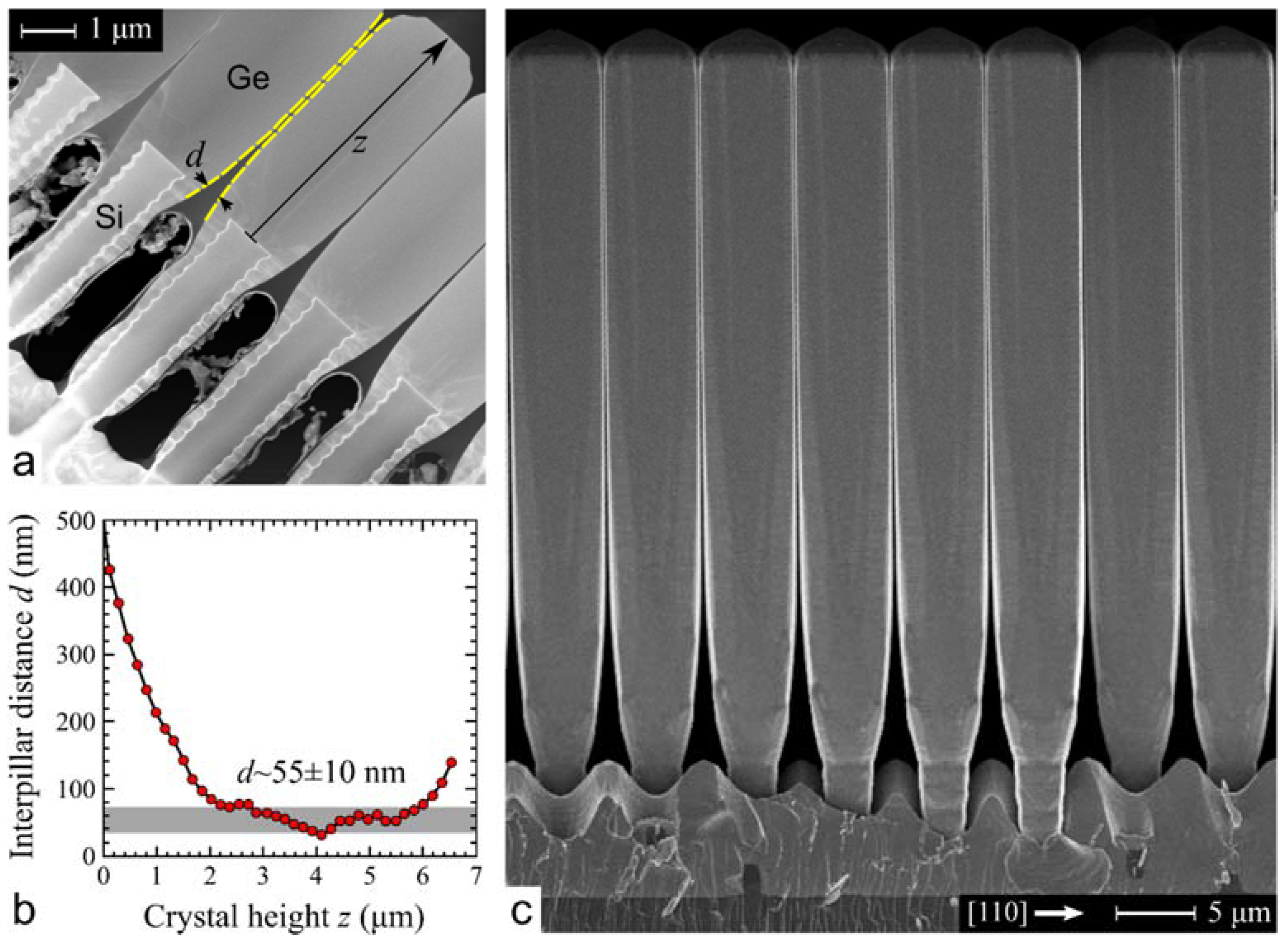
Two examples of Ge/Si heterostructures are reported in Figure 1a,c. In both cases, prior to deposition, a Si(001) substrate was deeply patterned, exploiting a Bosch process [13] resulting in ordered arrays of square-based 2 × 2 μm2 Si pillars, separated by 2 and 4 μm trenches. Ge was subsequently deposited by Low-Energy Plasma-Enhanced Chemical Vapour Deposition (LEPECVD). LEPECVD [14] allows for the grow of crystalline Ge under strong out-of-equilibrium conditions, determined by the high deposition rate (≈4 nm/s for both structures in Figure 1) and by the low deposition temperature (440 °C in Figure 1a; 490 °C in Figure 1c). Under such conditions, typical diffusion lengths are much smaller than the micrometric pillar sizes, so that the Ge crystal has a tendency to grow vertically [11] from the very beginning. Some lateral enlargement also takes place, leading to a progressive shrinking of the lateral distance between crystals growing on adjacent pillars. This causes a strong self-shielding effect ultimately leading to (almost) perfect vertical growth. Once vertical growth is established, the crystals can be grown for several dozens of microns without ever touching, separated by a very small gap (Figure 1b). The vertical morphology offers two key advantages with respect to common 2D layers. On one hand, the free surface surrounding the crystals allows for very efficient relaxation of the thermal-stress field [15,16,17,18], therefore avoiding cracking. On the other hand, 60° dislocations forming at the Ge/Si interface and laying on (111) planes, are confined to the bottom of the crystal only (no 60° defect can reach the region located at a height h >1.4 b, where b is the Si pillar base width). While 60° dislocations are the dominant linear defects in Ge/Si systems grown under typical conditions, the LEPECVD out-of-equilibrium conditions lead to the formation of perfectly vertical defects [19,20] which can thread through the whole pillar, reaching the topmost surface as shown in Figure 2a,b. However, also these dislocations can be expelled laterally, provided that the top facet of the pillar is not parallel to the (001) substrate during growth. This can be easily achieved by raising the growth temperature [12], as shown in Figure 2c. Fortunately, indeed, linear defects tend to follow the growth front, so that the problem of vertical dislocations can be easily solved by properly tuning the growth conditions eliminating the top (001) facet.
3D LEPECVD growth of vertical heterostructures is not limited to pure Ge: upon properly tuning the growth conditions, analogous crystals have been obtained for GexSi1−x alloys of various Ge-content x. Actually, growth at low x is even more convenient in terms of lateral expulsion of defects, as the aforementioned vertical dislocations are not formed [20]. This is explicitly shown in Figure 3, where the etch-pit distribution clearly shows the lateral expulsion of defects.
2.2. Other Deposition Techniques and Other Materials
The aim of this subsection is to show that (a) 3D heteroepitaxy is not achievable only by LEPECVD and that (b) a wide class of materials different from Ge/SiGe alloys can be grown in similar ways.
Let us first consider point (a). In Figure 4a a few representative snapshots of the morphology of a Ge crystal grown by Reduced-Pressure Chemical Vapour Deposition (RPVCD) on a 2 × 2 μm2 Si pillar are reported [21]. As the typical growth conditions in RPCVD are very different from LEPECVD in both terms of flux (lower) and temperature (higher), longer diffusion lengths make vertical growth more difficult. To limit horizontal growth and material diffusing from the top regions to the pillar bottom, growth was therefore performed on pillars whose lateral walls were oxidized.
In Figure 4b, results of a phase-field [22] growth simulation are displayed. Material deposition is modeled in terms of condensation from the gas phase, according to the local chemical potential , including anisotropies in the surface energy to induce spontaneous faceting [23]. The nice agreement between the model and the experiments of Figure 4a allowed for a detailed analysis, reported in Ref. [21], of both thermodynamic and kinetic factors influencing the crystal morphology, confirming that growth by RPCVD is closer to equilibrium with respect to LEPECVD.
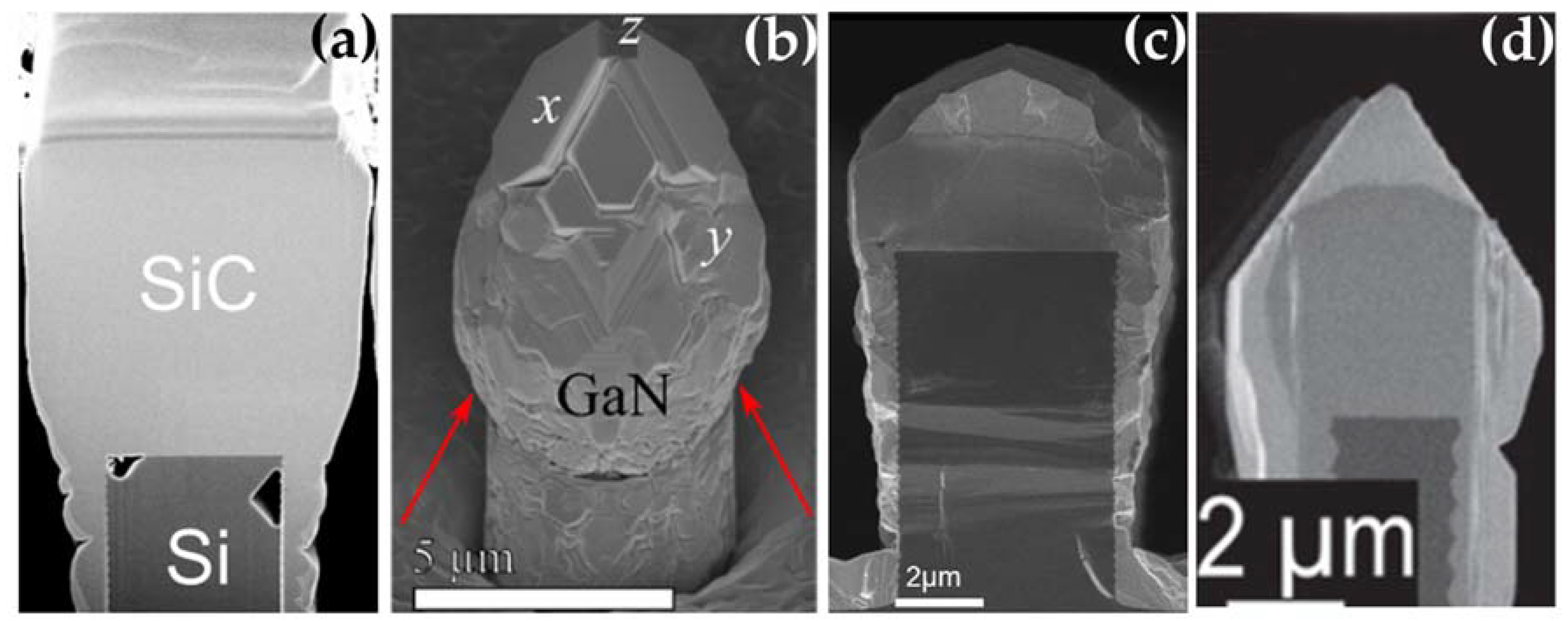
Let us now analyze the possibility to grow other materials. In Figure 5, the final morphology of SiC [24] (panel a), GaN [25] (panel b), GaAs [26,27] (panel c), and GaAs/Ge [28,29] (panel d) crystals grown on Si pillars is displayed. The various deposition techniques are listed in the caption. All such materials are extremely interesting for applications (in fields such as power electronics and optics), and the urge of lowering the typical defect density while attempting integration on Si is perhaps even more important than the already discussed Ge case.
Despite the successful growth of 3D crystals reported in Figure 5, it is important to emphasize that 3D heteroepitaxy of binary materials such as SiC or GaAs still demands for a significant effort in order to control the additional defects, such as stacking faults and/or anti-phase domains, which are typical of these systems while playing a lesser role in SiGe.
2.3. Suspended Films
We have pointed out that micron-size vertical crystals can be grown stress-free and without dislocations in the majority of their volume. These are surely appealing features from the point of view of applications. However, mainstream technology is mainly developed to handle planar 2D layers. With this in mind, researchers have also started to look at the possibility to form suspended films, formed by merging of adjacent vertical crystals. Note that if crystals are first vertically grown above the height needed to laterally expel dislocations (see Figure 3) and merging occurs only at the topmost regions, the suspended film would not inherit dislocations formed at the pillar/crystal interface.
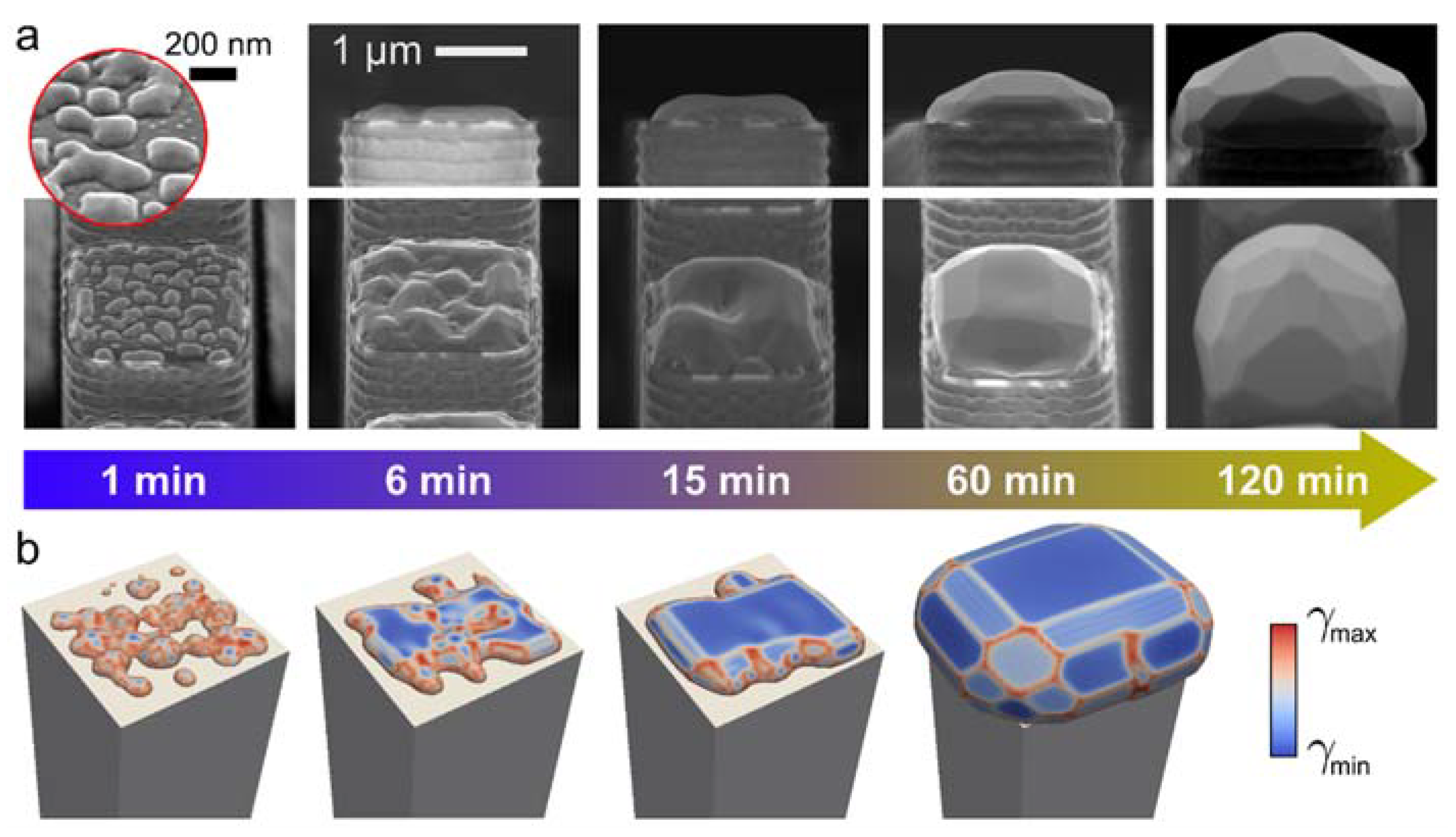
The suspended film displayed in Figure 6 was obtained [30] by prolongated high-temperature annealing of vertical Ge crystals on Si pillars. Temporal snapshots of the evolution are also displayed, together with a corresponding continuum simulation [31] (panel b). The latter was performed exploiting a diffusion-equation approach, implemented in a phase-field framework [22], where the only contribution to the chemical potential μ (determining material flow) was the Mullins [32] term , where is the local curvature and the surface-energy density. Therefore, the almost perfect agreement between experiments and theory signals that the whole material redistribution leading to the merging process is determined solely by surface-curvature. The evolution displayed in Figure 6 was subsequently simulated [33] by also taking into account surface-energy anisotropy [23], yielding results even closer to the experimental ones.
It has been further demonstrated that merging can also be obtained directly during growth (by raising the growth temperature) [21,31]. The suspended film is found [18] to still profit of the ability of the underlying pillars to release thermal strain by tilting. Despite displaying a good crystal quality, suspended films do display some defects, likely to be created during actual merging [21]. Present efforts are dedicated to minimizing such defects by adding further control on growth conditions and by exploiting fully dislocation-free micro-crystals using the technique described in the next Section.
3. Graded, Vertical Heterostructures
3.1. Elastic vs. Plastic Relaxation: Theory
Vertical heterostructures (VHEs) are characterized by the presence of free surfaces allowing for the partial elastic relaxation of in-plane strains/stresses. Indeed, at variance with heteroepitaxial films, these structures can expand/contract laterally to partially accommodate lattice misfits. This also leads to a significant compliance mechanism, i.e., a redistribution of the misfit strain between layers having a different lattice parameter. As a result, the tendency towards plastic relaxation is expected to be inhibited.
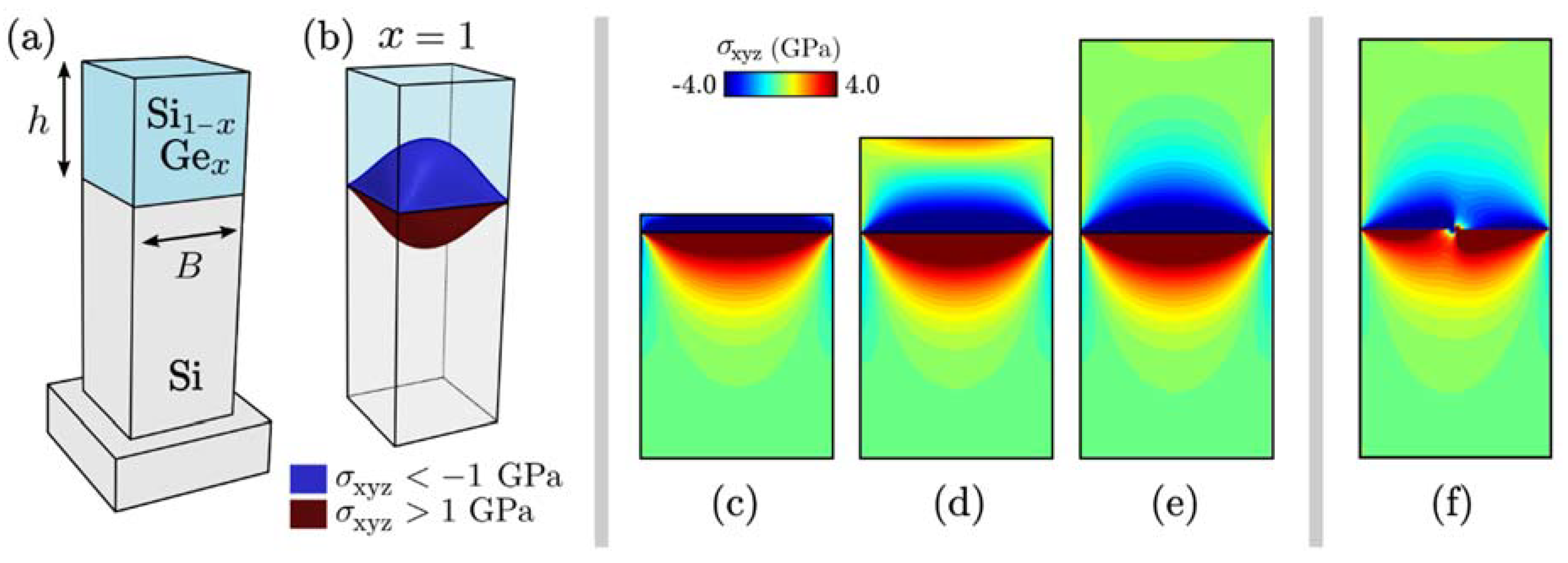
These properties of VHEs allow for dislocation-free structures, provided that the lateral size is smaller than critical values depending on the materials and on the misfit strain as discussed in [34]. In Ref. [35] these critical sizes were computed for the specific case of Si1−xGex/Si VHEs by means of a quasi-3D approach allowing for detailed estimation of thermodynamic plasticity onsets. This method exploits isotropic linear elasticity theory and Finite Element Method (FEM) calculations (see also [36]) while VHEs are modeled by simplified geometries as in Figure 7a. However, notice that it can be straightforwardly used to investigate realistic shapes as shown in Refs. [37,38,39].
Following the work in [35], the typical elastic field of VHEs as in Figure 7a can be computed by FEM calculations and it is illustrated in Figure 7b for a pure Ge epilayer by means of the hydrostatic stress . It consists of a compressive and a tensile region above and below the Si1−xGex/Si interface, respectively. The resulting elastic field is self-similar, i.e., its qualitative features depend on the height-to-base aspect-ratio and it can be adapted to any specific size upon proper rescaling. Figure 7c–e shows the different distributions of in the central slice of a VHE for , , and , respectively.
The tendency towards plastic relaxation can be quantified by the formation energy, , computed in the 2D central slice of the full 3D geometry representing the VHE. is the elastic energy of the coherent system, i.e., without dislocations. is the elastic energy accounting for the presence of a 60° dislocation at the interface, known to be always favored in Si1−xGex/Si systems with respect to other dislocation types [40]. In particular, the stress field of the coherent system is evaluated in the 3D structure, as in Figure 7b, and it is extracted in the central slice to compute . Then, the same elastic field is superimposed to the one of a straight (perpendicular to the 2D slice) 60° dislocation lying at the center of the Si1−xGex/Si interface, as in Figure 7f, to compute . When , plastic relaxation is energetically favored, and dislocations are expected. The central position for the dislocation is the minimum energy configuration for relatively small and large values of . For intermediate aspect-ratios, the minimum energy configuration may be shifted towards the sidewalls. However, the central position gives a very good approximation of the global energy minimum. Notice that computing in the central slice corresponds to evaluate an energy per unit length of the dislocation misfit segment. Therefore, this approach describes the tendency of a dislocation to elongate, resembling the classical method used to evaluate the critical thickness for the insertion of dislocation, , in planar structures [5,41]. Further details about the method, its assessment, and the simulation setup can be found in Refs. [35,36].
With the approach described above, can be calculated as a function of the Ge content in the Si1−xGex epilayer, , and the lateral size of the VHE, . Moreover, it is possible to determine the critical lateral size as a function of , namely . These quantities are shown in Figure 7: is illustrated by means of dashed black isolines, while corresponds to the solid red line. Above the red curve, for thicknesses smaller than , at which plasticity is expected to set in. Below the red curve, for any thickness of the epilayer, i.e., the corresponding VHE is predicted to be always coherent.
For a fixed Ge content value , we then expect a coherent structure when . VHEs with a larger are predicted to have dislocations with a critical thickness that is larger than the corresponding one in a planar configuration, achieved in the limit. Similar arguments apply for a targeted lateral size . A VHE with a Ge content x smaller than the critical one as a function of the base, (), is predicted to be coherent, while dislocations are expected for (). From the results reported in Figure 8, such critical curves can be fitted as follows:
with , , nm (the latter corresponding to the predicted critical base for a pure-Ge pillar epilayer) and
with , . Being these values based on a purely energetic balance, and due to the assumption of the model, they are expected to be quantitative lower bounds indicating the worst possible scenario to growth coherent VHEs.
From a technological point of view, and set the limits for the realization of fully-coherent VHE. Let us focus on the target of a Si1−xGex epilayer on Si with Ge content . With the configuration of VHEs as discussed so far, this can be achieved only up to a lateral size of that is less than nm for a pure-Ge epilayer. However, looking at the elastic field of the VHEs in Figure 7, one can easily notice that for a thickness , i.e., for an aspect ratio , the top of the epilayer is fully relaxed. Moreover, this is a purely geometric effect that is not dependent on or [34]. So that, even for basis larger than , one can think about growing a first coherent layer with up to . Then, as far as the top of the structure is relaxed, a second layer can be considered, and the vertical structure is predicted to be coherent provided that the increase in the Ge content with respect to the first layer is lower than , i.e., the second layer can have a Ge content such as . So that a coherent structure with a Ge content up to can be grown. If this Ge content is smaller then , further layers can be considered exploiting the same idea up to the desired target. The discrete number of layers required to reach for a given B is then given by the simple relation .
This concept has been explicitly verified in Ref. [35] by checking the formation energy at different interfaces and also investigating in the detail the elastic relaxation of layers with different thicknesses. In experiments aiming at the growth of SiGe structures, a continuous grading of the Ge content is often performed. From the aforementioned results, and under the assumption of ideal layer, the grading rate () to achieve a fully coherent structure up to a Ge content can be easily calculated as
where the second equal sign holds true when removing the ceiling function in as the constraint of a discrete number of buffer layers is not required when speaking about the continuous grading rate. Notice that, the resulting expression of the grading rate is a function of the size but it is independent of . The calculations reported in Figure 8 are limited to structures with nm. However, by assuming that the equation for and are still valid for larger basis, recipes to grow fully-coherent VHEs can be provided for any size. In Table 1 the prediction about and , as well as and the total thickness computed as to obtain pure Ge (), are reported for some representative values of (larger than nm for which ). It is worth mentioning that once a dislocation-free structure is obtained following the recipes in Table 1, any thickness of additional pure Ge can be deposited, still resulting in a dislocation-free structure. Indeed, the top of this structure is fully relaxed and made of pure Ge, so that further Ge deposition would result, de facto, in a homoepitaxial growth. However, notice that when approaching values of in the order of ten microns, become very large and it is practically unfeasible for applications.
3.2. Dislocation-Free Graded Heterostructures
The theoretical recipe for growing dislocation-free crystals (see Table 1) was experimentally demonstrated in Ref. [42] and further analyzed in Ref. [43]. The target Ge content was set to 40%, and a Ge grading rate GR = 1.5%/μm was employed. Two sets of samples were considered. In case 1 (2) the initial Si pillar was 2 μm (5 μm in case 2) wide, while the deposited SiGe crystal grew laterally reaching a final width of 5.5 μm (8.0 μm). According to the theoretical estimate reported in Table 1, case 1 should lead to dislocation-free crystals, at variance with case 2. This was exactly the case, as demonstrated in Figure 9.
The result displayed in Figure 9 is of particular importance as it directly demonstrates the possibility to grow micron-sized heterostructures completely free of dislocations, in spite of the large lattice mismatch. The misfit strain is only accommodated by lateral elastic relaxation. More recently, the same result was achieved also for higher lattice mismatches (up to 80% Ge content) [44]. In principle, there is no limitation in the maximum lattice mismatch that can be relaxed or in the width of the SiGe crystal. In practice, however, one is limited by the need to grow very tall crystals (Table 1). To overcome this problem, attempts were made to lower the tendency towards inserting dislocations by changing the shape of the Si pillars. This led to interesting and unexpected results, reported in the next Section.
4. Deposition on Under-Etched Pillars
4.1. Graded Heterostructures on Under-Etched Pillars: Experimental Results
As discussed in the previous section, vertical heterostructures can exploit lateral surfaces to relax the misfit strain also in the in-plane direction at variance with planar films. With the aim of increasing the compliance of the Si pillars, vertical Si structures (Figure 10a) were suitably under-etched (exploiting a two-step dry etching process [45]) prior to SiGe deposition, leading to the necked structures reported in Figure 10b. Graded vertical heterostructures where then grown on both “standard” (Figure 10d) and under-etched (Figure 10c) pillars of different width, using a grading rate GR = 1.5%Ge/μm and reaching a final 40% Ge content. The dislocation density was inferred by etch-pits counts, leading to the results displayed in Figure 11.
Measurements of the dislocation density (DD) and the dislocation-free probability (DFP) are reported in Figure 11, distinguishing between estimate relative to the actual SiGe crystal (panel a and b) and to the Si pillar (panel c and d). Results clearly show the key role played by morphology. In the presence of the “neck” (under-etched morphology), indeed, a large fraction of defects is transferred from the SiGe crystal to the underlying Si pillar, the effect being present also for large pillar widths. The effect is nicely evidences by the SEM image in panel (e), where etch pits are clearly distinguished. Notice that also for a base as large of 10 μm, a considerable fraction of the crystals grown on under-etched pillars is dislocation free, as evidenced by the value of the DFP reported in Figure 11b.
Summarizing the results discussed so far, by using a GR of 1.5%Ge/μm one can grow fully dislocation-free heterostructures, where “fully” means that defects are not present in the deposited crystal as well as in the pillar, up to to ~5 μm. If one is willing to grow larger vertical heterostructures, then suitable under-etching allows for enlarging the critical width to 10 μm. In this case, however, only the crystal is dislocation-free, while defects are introduced in the Si pillar. Still, this could be still very appealing for applications exploiting only the SiGe crystal as active region. In the following the theoretical justification of the effect produced by introducing substrate necking is discussed.
4.2. Graded Heterostructures on Under-Etched Pillars: Theoretical Interpretation
The role played by necking was theoretically investigated in Ref. [46]. Here we briefly summarize the main findings. In Figure 12 we report the hydrostatic stress maps computed by solving isotropic elasticity theory by finite element methods, simulating the same grading rate used in the experiments (GR = 1.5%Ge/μm).
In Figure 12a, a standard “vertical” pillar morphology is considered, while in all other panels the effect of under-etching was taken into account. As in Section 3.1, the pillar morphology is simplified: instead of considering the enlargement of the width (Figure 10c) caused by deposition, we fix it and repeat calculations for the lowest (Lm) and largest (LM) dimensions. Figure 12 shows that necking changes the local misfit relaxation both in Si and in SiGe, introducing a strongly compressed region (blue color in the maps) within Si. This has a profound influence on the nucleation and distribution of dislocations.
In SiGe/Si systems, misfit is typically relaxed by 60° dislocations. In the 2D model used to generate all results discussed in this Section, the dislocation line is assumed to run in the third direction (perpendicular to the Figure, in Figure 12), and there exist two possible glide planes (G.P. 1 and G.P. 2 in Figure 12e) and four Burgers vectors, called b1, b2, b3, and b4 in Figure 12e. Two of them (b1 and b2) provide expansion of the region above the core, the others have the opposite effect. These are the ones more often encountered in SiGe/Si planar films or in vertical pillars, as the tensile strain introduced by the dislocations reduces the lattice compression due to lattice-parameter misfit. The presence of the strong compressive stress in under-etched Si pillars (Figure 12b–d), instead, reverses the sign of the lowest-energy defects. This is shown in Figure 13: insertion of the same dislocations relaxing SiGe/Si films or SiGe on vertical pillars (“normal” case in Figure 13) raises the energy of the system for both explored sizes. On the contrary, the introduction of dislocations with opposite sign of the in-plane component of the Burgers vector (b3, or b4, helping to relax compression in the Si region) becomes energetically favored beyond a critical height. The difference in energy between the system with and without a dislocation located at its minimum-energy position (∆Emin), indeed, becomes negative. In Ref. [46] it was shown by dislocation dynamics simulations that accounting for the change in Burgers vector orientation is fundamental in order to explain the typical dislocation distributions experimentally observed in SiGe crystals grown on underetched Si pillars. The typical pile-up in the Si region, well evident in Figure 11e, is indeed compatible only with dislocations removing half atomic plane in the Si region (Burgers vector b3).
5. Conclusions and Perspectives
In this paper we reviewed a five-years-long investigation on the 3D growth of Ge, GeSi and Ge-graded crystals on deeply patterned substrates, where proper deposition conditions and patterning geometry allows for a dense array of vertical structures. This high aspect ratio strategy, in turn, exploits the termination of misfit dislocations on lateral sidewalls, the accommodation of the thermal strain, and even the elimination of plastic relaxation by fully elastic misfit-strain relaxation, in case of graded deposition. The important result is that, whenever a device application requires a dense array of Ge, or GeSi, individual crystals, such as the case of X-ray detectors, or infrared single-photon-avalanche-detectors (SPAD), this proof-of-concept is ready to be transferred to the stage of the industrial prototype. In fact, for both the applications mentioned above are currently the subject of projects devoted to increase the technology readiness level.
However, more widespread applications may arise if the concept is extended to other heteroepitaxial binary materials, such as the cubic SiC for power electronics, GaN and GaAs for optoelectronics. In Section 2.2 we have reviewed a set of promising, preliminary attempts to grow such materials. However, a convincing proof-of-concept is still missing, due to the fact that other extended defects, such as stacking faults and twins, or anti-phase domains may occur, and that the extended lateral sidewalls may act as a source of them. To this end, a merging of the individual crystals into a continuous suspended layer should be eventually obtained, taking the risk that in the merging process additional dislocations, or other extended defects, may originate, as it has been shown for the case of Ge, probably because of some crystal tilting. The efforts and the timescale required for such an improvement are probably much larger than the ones devoted in obtaining defect-free Ge crystals.
Still, a lot of new scientific knowledge is likely to be produced when exploring the features of 3D heteroepitaxy of binary materials on deeply patterned substrates, and vertical growth by selected area depositions. In our opinion, the morphologies arising from tuning the competitive growth of neighboring facets by suitable deposition conditions may result in exciting and, possibly, promising issue to extend this Ge-based technique to other materials.
6. Patents
H. von Känel and L. Miglio, Dislocation and stress management by mask-less processes using substrate patterning and methods for device fabrication, PCT/IB2011/000895”.
Funding
This research was funded by Regione Lombardia, under the TEINVEIN project, Call Accordi per la Ricerca e l’Innovazione, co-funded by POR FESR 2014-2020 (ID: 242092), by the European Union (Horizon-2020 FET “μ-Spire” project, ID: 766955 and CHALLENGE project, ID: 720827, NMBP-02-2016), by the Swiss National Science Foundation (Sinergia Project NOVIPIX CRSII2 147639), and by the Alexander von Humboldt Foundation (Postdoctoral Research Fellowship awarded to M.S.).
Conflicts of Interest
The authors declare no conflict of interest.
References
- Kazior, T.E. Beyond CMOS: Heterogeneous integration of III–V devices, RF MEMS and other dissimilar materials/devices with Si CMOS to create intelligent microsystems. Philos. Trans. R. Soc. A 2014, 372. [Google Scholar] [CrossRef] [PubMed]
- Wang, G.; Loo, R.; Simoen, G.; Souriau, L.; Caymax, M.; Heyns, M.M.; Blanpain, P. A model of threading dislocation density in strain-relaxed Ge and GaAs epitaxial films on Si(100). Appl. Phys. Lett. 2009, 94, 102115. [Google Scholar] [CrossRef]
- Speck, J.S.; Brewer, M.A.; Beltz, G. Scaling laws for the reduction of threading dislocation densities in homogeneous buffer layers. J. Appl. Phys. 1996, 80, 3808. [Google Scholar] [CrossRef]
- Fitzgerald, E.A.; Xie, Y.H.; Green, M.L.; Brasen, D.; Kortan, A.R.; Michel, J.; Mii, Y.J.; Weir, B.E. Totally relaxed GexSi1−x layers with low threading dislocation densities grown on Si substrates. Appl. Phys. Lett. 1991, 59, 811. [Google Scholar] [CrossRef]
- Fitzgerald, E.A. Dislocations in strained-layer epitaxy: Theory, experiment, and applications. Mater. Sci. Rep. 1991, 7, 87–142. [Google Scholar] [CrossRef]
- Tersoff, J. Dislocations and strain relief in compositionally graded layers. Appl. Phys. Lett. 1993, 62, 693. [Google Scholar] [CrossRef]
- Yamamoto, Y.; Kozlowski, G.; Zaumseil, P.; Tillack, B. Low threading dislocation Ge on Si by combining deposition and etching. Thin Solid Films 2012, 520, 3216–3221. [Google Scholar] [CrossRef]
- Langdo, T.A.; Leitz, C.W.; Currie, M.T.; Fitzgerald, E.A. High quality Ge on Si by epitaxial necking. Appl. Phys. Lett. 2000, 76, 3700. [Google Scholar] [CrossRef]
- Park, J.-S.; Curtin, M.; Adekore, B.; Carroll, M.; Lochtefeld, A. Defect reduction of selective Ge epitaxy in trenches on Si(001) substrates using aspect ratio trapping. Appl. Phys. Lett. 2007, 90, 052133. [Google Scholar] [CrossRef]
- Linthicum, K.; Gehrke, T.; Thomson, D.; Carlson, E.; Rajagopal, P.; Smith, T.; Batchelor, D.; Davis, R. Pendeoepitaxy of gallium nitride thin films. Appl. Phys. Lett. 1999, 75, 196. [Google Scholar] [CrossRef]
- Falub, C.V.; von Känel, H.; Isa, F.; Bergamaschini, R.; Marzegalli, A.; Chrastina, D.; Isella, G.; Müller, E.; Niedermann, P.; Miglio, L. Scaling hetero-epitaxy from layers to three-dimensional crystals. Science 2012, 335, 1330–1334. [Google Scholar] [CrossRef] [PubMed] [Green Version]
- Bergamaschini, R.; Isa, F.; Falub, C.V.; Niedermann, P.; Müller, E.; Isella, G.; von Känel, H.; Miglio, L. Self-aligned Ge and SiGe three-dimensional epitaxy on dense Si pillar arrays. Surf. Sci. Rep. 2013, 68, 390–417. [Google Scholar] [CrossRef]
- Laermer, F.; Schilp, A. Method of Anisotropically Etching Silicon. U.S. Patent No. 5501893, 26 March 1996. [Google Scholar]
- Rosenblad, C.; von Känel, H.; Kummer, M.; Dommann, A.; Müller, E. A plasma process for ultrafast deposition of SiGe graded buffer layers. Appl. Phys. Lett. 2000, 76, 427. [Google Scholar] [CrossRef]
- Falub, C.V.; Meduňa, M.; Chrastina, D.; Isa, F.; Marzegalli, A.; Kreiliger, T.; Taboada, A.G.; Isella, G.; Miglio, L.; Dommann, A.; et al. Perfect crystals grown from imperfect interfaces. Sci. Rep. 2013, 3, 2276. [Google Scholar] [CrossRef] [PubMed] [Green Version]
- Meduna, M.; Falub, C.V.; Isa, F.; Marzegalli, A.; Chrastina, D.; Isella, G.; Miglio, L.; Dommann, A.; von Känel, H. Lattice bending in three-dimensional Ge microcrystals studied by X-ray nanodiffraction and modelling. J. Appl. Cryst. 2016, 49, 976–986. [Google Scholar] [CrossRef]
- Meduna, M.; Isa, F.; Jung, A.; Marzegalli, A.; Albani, M.; Isella, G.; Zwelacker, K.; Miglio, L.; von Känel, H. Lattice tilt and strain mapped by X-ray scanning nanodiffraction in compositionally graded SiGe/Si microcrystals. J. Appl. Cryst. 2018, 51, 368–385. [Google Scholar] [CrossRef]
- Marzegalli, A.; Cortinovis, A.; Basset, F.B.; Bonera, E.; Pezzoli, F.; Scaccabarozzi, A.; Isa, F.; Isella, G.; Zaumseil, P.; Capellini, G.; et al. Exceptional thermal strain reduction by a tilting pillar architecture: Suspended Ge layers on Si(001). Mater. Des. 2017, 116, 144–151. [Google Scholar] [CrossRef]
- Marzegalli, A.; Isa, F.; Groiss, H.; Müller, E.; Falub, C.V.; Taboada, A.G.; Niedermann, P.; Isella, G.; Schaeffler, F.; Montalenti, F.; et al. Unexpected Dominance of Vertical Dislocations in High-Misfit Ge/Si(001) Films and Their Elimination by Deep Substrate Patterning. Adv. Mater. 2013, 25, 4408–4412. [Google Scholar] [CrossRef] [PubMed]
- Isa, F.; Marzegalli, A.; Taboada, A.G.; Falub, C.V.; Isella, G.; Montalenti, F.; von Känel, H.; Miglio, L. Onset of vertical threading dislocations in Si1−xGex/Si(001) at a critical Ge concentration. APL Mater. 2013, 1, 052109. [Google Scholar] [CrossRef]
- Skibitzki, O.; Capellini, G.; Yamamoto, Y.; Zaumseil, P.; Schubert, M.A.; Schroeder, T.; Ballabio, A.; Bergamaschini, R.; Salvalaglio, M.; Miglio, L.; et al. Reduced-Pressure Chemical Vapor Deposition Growth of Isolated Ge Crystals and Suspended Layers on Micrometric Si Pillars. ACS Appl. Mater. Interfaces 2016, 8, 26374–26380. [Google Scholar] [CrossRef] [PubMed]
- Li, B.; Lowengrub, J.; Ratz, A.; Voigt, A. Geometric evolution laws for thin crystalline films: Modeling and numeric. Commun. Comput. Phys. 2009, 6, 433. [Google Scholar]
- Salvalaglio, M.; Backofen, R.; Bergamaschini, R.; Montalenti, F.; Voigt, A. Faceting of Equilibrium and Metastable Nanostructures: A Phase-Field Model of Surface Diffusion Tackling Realistic Shapes. Cryst. Growth Des. 2015, 15, 2787–2794. [Google Scholar] [CrossRef]
- Von Känel, H.; Isa, F.; Falub, C.V.; Barthazy, E.J.; Müller, E.; Chrastina, D.; Isella, G.; Kreiliger, T.; Taboada, A.G.; Meduna, M.; et al. Three-dimensional Epitaxial Si1−xGex, Ge and SiC Crystals on Deeply Patterned Si Substrates. ECS Trans. 2014, 64, 631–648. [Google Scholar] [CrossRef]
- Isa, F.; Cheze, C.; Siekacz, M.; Hauswald, C.; Laehnemann, J.; Fernandez-Garrido, S.; Kreliger, T.; Ramsteiner, M.; Arroyo Rojas Da Silva, A.; Brandt, O.; Isella, G.; et al. Integration of GaN Crystals on Micropatterned Si(0 0 1) Substrates by Plasma-Assisted Molecular Beam Epitaxy. Cryst. Growth Des. 2015, 15, 4886–4892. [Google Scholar] [CrossRef]
- Bietti, S.; Scaccabarozzi, A.; Frigeri, C.; Bollani, M.; Bonera, E.; Falub, C.V.; von Känel, H.; Miglio, L.; Sanguinetti, S. Monolithic integration of optical grade GaAs on Si (001) substrates deeply patterned at a micron scale. Appl. Phys. Lett. 2013, 103, 262106. [Google Scholar] [CrossRef]
- Bergamaschini, R.; Bietti, S.; Castellano, A.; Frigeri, C.; Falub, C.V.; Scaccabarozzi, A.; Bollani, M.; von Känel, H.; Miglio, L.; Sanguinetti, S. Kinetic growth mode of epitaxial GaAs on Si(001) micro-pillars. J. Appl. Phys. 2016, 120, 245702. [Google Scholar] [CrossRef]
- Taboada, A.G.; Kreiliger, T.; Falub, C.V.; Isa, F.; Salvalaglio, M.; Wevior, L.; Fuster, D.; Richter, M.; Uccelli, E.; Niedermann, P.; et al. Strain relaxation of GaAs/Ge crystals on patterned Si substrates. Appl. Phys. Lett. 2014, 104, 022112. [Google Scholar] [CrossRef] [Green Version]
- Taboada, A.G.; Meduna, M.; Salvalaglio, M.; Isa, F.; Kreiliger, T.; Falub, C.V.; Barthazy Meier, E.; Müller, E.; Miglio, L.; Isella, G.; et al. GaAs/Ge crystals grown on Si substrates patterned down to the micron scale. J. Appl. Phys. 2016, 119, 055301. [Google Scholar] [CrossRef]
- Salvalaglio, M.; Bergamaschini, R.; Isa, F.; Scaccabarozzi, A.; Isella, G.; Backofen, R.; Voigt, A.; Montalenti, F.; Capellini, G.; Schroeder, T.; et al. Engineered Coalescence by Annealing 3D Ge Microstructures into High-Quality Suspended Layers on Si. ACS Appl. Mater. Interfaces 2015, 7, 19219–19225. [Google Scholar] [CrossRef] [PubMed]
- Bergamaschini, R.; Salvalaglio, M.; Backofen, R.; Voigt, A.; Montalenti, F. Continuum modelling of semiconductor heteroepitaxy: An applied perspective. Adv. Phys. X 2016, 1, 331–367. [Google Scholar] [CrossRef]
- Mullins, W.W. Theory of Thermal Grooving. J. Appl. Phys. 1957, 28, 333. [Google Scholar] [CrossRef]
- Salvalaglio, M.; Bergamaschini, R.; Backofen, R.; Voigt, A.; Montalenti, F.; Miglio, L. Phase-field simulations of faceted Ge/Si-crystal arrays, merging into a suspended film. Appl. Surf. Sci. 2017, 391, 33–38. [Google Scholar] [CrossRef]
- Glas, F. Critical dimensions for the plastic relaxation of strained axial heterostructures in free-standing nanowires. Phys. Rev. B 2006, 74, 121302. [Google Scholar] [CrossRef]
- Salvalaglio, M.; Montalenti, F. Fine control of plastic and elastic relaxation in Ge/Si vertical heterostructures. J. Appl. Phys. 2014, 116, 104306. [Google Scholar] [CrossRef]
- Gatti, R.; Marzegalli, A.; Zinovyev, V.A.; Montalenti, F.; Miglio, L. Modeling the plastic relaxation onset in realistic SiGe islands on Si(001). Phys. Rev. B 2008, 78, 184104. [Google Scholar] [CrossRef]
- Montalenti, F.; Salvalaglio, M.; Marzegalli, A.; Zaumseil, P.; Capellini, G.; Schülli, T.U.; Schubert, M.A.; Yamamoto, Y.; Tillack, B.; Schroeder, T. Fully coherent growth of Ge on free-standing Si(001) nanomesas. Phys. Rev. B 2014, 89, 014101. [Google Scholar] [CrossRef]
- Scarpellini, D.; Somaschini, C.; Fedorov, A.; Bietti, S.; Frigeri, C.; Grillo, V.; Esposito, L.; Salvalaglio, M.; Marzegalli, A.; Montalenti, F.; et al. InAs/GaAs Sharply Defined Axial Heterostructures in Self-Assisted Nanowires. Nano Lett. 2015, 15, 3677–3683. [Google Scholar] [CrossRef] [PubMed]
- Niu, G.; Capellini, G.; Lupina, G.; Niermann, T.; Salvalaglio, M.; Marzegalli, A.; Schubert, M.A.; Zaumseil, P.; Krause, H.-M.; Skibitzki, O.; et al. Photodetection in Hybrid Single-Layer Graphene/Fully Coherent Germanium Island Nanostructures Selectively Grown on Silicon Nanotip Patterns. ACS Appl. Mater. Interfaces 2016, 8, 2017–2026. [Google Scholar] [CrossRef] [PubMed]
- Hirth, J.P.; Lothe, J. Theory of Dislocations; Krieger Publishing Company: Malabar, FL, USA, 1992; ISBN 0894646176. [Google Scholar]
- Matthews, J.W.; Blakeslee, A.E. Defects in epitaxial multilayers. J. Cryst. Growth 1974, 27, 118–125. [Google Scholar] [CrossRef]
- Isa, F.; Salvalaglio, M.; Arroyo Rojas Dasilva, Y.; Meduna, M.; Barget, M.; Jung, A.; Kreiliger, T.; Isella, G.; Erni, R.; Pezzoli, F.; et al. Highly Mismatched, Dislocation-Free SiGe/Si Heterostructures. Adv. Mater. 2016, 28, 884–888. [Google Scholar] [CrossRef] [PubMed]
- Isa, F.; Salvalaglio, M.; Arroyo Rojas Dasilva, Y.; Jung, A.; Isella, G.; Erni, R.; Niedermann, P.; Groening, P.; Montalenti, F.; von Känel, H. From plastic to elastic stress relaxation in highly mismatched SiGe/Si heterostructures. Acta Mater. 2016, 114, 97–105. [Google Scholar] [CrossRef] [Green Version]
- Isa, F.; Jung, A.; Salvalaglio, M.; Arroyo Rojas Dasilva, Y.; Marozau, I.; Meduna, M.; Barget, M.; Marzegalli, M.; Isella, G.; Erni, R.; et al. Strain Engineering in Highly Mismatched SiGe/Si Heterostructures. Mater. Sci. Semicond. Process. 2017, 70, 117–122. [Google Scholar] [CrossRef]
- Isa, F.; Salvalaglio, M.; Arroyo Rojas Dasilva, Y.; Jung, A.; Isella, G.; Erni, R.; Timotijevic, B.; Niedermann, P.; Groening, P.; Montalenti, F.; et al. Enhancing elastic stress relaxation in SiGe/Si heterostructures by Si pillar necking. Appl. Phys. Lett. 2016, 109, 182112. [Google Scholar] [CrossRef]
- Rovaris, F.; Isa, F.; Gatti, R.; Jung, A.; Isella, G.; Montalenti, F.; von Känel, H. Three-dimensional SiGe/Si heterostructures: Switching the dislocation sign by substrate under-etching. Phys. Rev. Mater. 2017, 1, 073602. [Google Scholar] [CrossRef]
Figure 1.
Self-aligned vertical growth of Ge micro-crystals on 2 × 2 µm2 Si pillars, 8 µm deep. (a) Dark-field STEM view of 7 µm tall Ge crystals grown at 440 °C on pillars spaced by 2 µm. (b) Plot of the distance between the adjacent crystals in panel a. (c). SEM lateral view of 50 µm tall Ge crystals grown at 490 °C on pillars spaced by 4 µm. Reproduced with permission from [12].

Figure 2.
Dislocations in Ge micro-crystals on Si pillars. (a) Bright-field TEM cross-section in the Ge[220] Bragg condition showing both 60° and vertical dislocations. AFM view of the Ge crystal top after defect etching in iodine solution for (b) a (001) flat-top morphology obtained by growing at 440 °C and (c) a {113} pyramidal shape obtained at 560 °C. The schematics illustrate the different propagation of dislocation lines with respect to the faceting of the growth front. Reproduced with permission from [12].

Figure 3.
Lateral expulsion of dislocations. SEM image showing confinement of etch-pits in the bottom pillar region for a Ge0.2Si0.8/Si(001) crystal. Reproduced with permission from [20]. American Institute of Physics.
Figure 3.
Lateral expulsion of dislocations. SEM image showing confinement of etch-pits in the bottom pillar region for a Ge0.2Si0.8/Si(001) crystal. Reproduced with permission from [20]. American Institute of Physics.

Figure 4.
Growth sequence of a Ge micro-crystal on a 2 × 2 µm2 Si pillar by RPCVD. (a) Lateral and perspective SEM views of samples after deposition of different duration. Multiple crystal seeds are observed at the early stages, coalescing into a single faceted structure later on. (b) Profiles obtained by a phase-field simulation of crystal growth, matching the experimental behavior. Reproduced with permission from [21]. American Chemical Society.

Figure 5.
Deposition of several different materials on Si pillars. (a) SiC/Si, deposited by hot-wall Chemical Vapour Deposition. Reproduced with permission from [24]. Electrochemical Society (b) GaN/Si, deposited by plasma-assisted molecular beam epitaxy. Reproduced with permission from [25]. American Chemical Society (c) GaAs/Si, deposited by molecular beam epitaxy. Reproduced with permission from [26]. Copyright 2013, the American Institute of Physics (d) GaAs/Ge/Si, where Ge was deposited by LEPECVD and GaAs by metal-organic vapour-phase epitaxy. Reproduced with permission from [28]. American Institute of Physics.

Figure 6.
Coalescence of vertically-aligned Ge micro-crystals into a suspended film. (a) Top and (b) lateral SEM images of the as-grown crystals and of identical samples after annealing of different duration. (c) Evolution sequence obtained by a phase-field simulation of surface diffusion. First, local rounding of the facets occurs; then, connection bridges form between neighboring crystals leaving holes, that are finally filled by material flow. Reproduced with permission from [30]. American Chemical Society.

Figure 7.
Theoretical modeling of VHEs and stress fields. (a) Simplified geometry of VHEs used to perform the theoretical analysis. (b) Illustrative map of the hydrostatic stress in a VHE as in panel (a) with . (c–e) in the central slice of a coherent 3D VHE as in panel (a,b) with an aspect-ratio equal to 0.1, 0.5 and 1.0 respectively. (f) as in panel (e) superposed to the hydrostatic stress field induced by a dislocation lying at the interface ( nm). Reproduced with permission from [35]. American Institute of Physics.

Figure 8.
Model results. Critical pillar base as a function of the Ge content x (solid red curve) and critical thickness of Si1−xGex/Si VHEs as function of B and x (dashed black isolines, numbers correspond to expressed in nm). Reproduced with permission from [35]. American Institute of Physics.
Figure 8.
Model results. Critical pillar base as a function of the Ge content x (solid red curve) and critical thickness of Si1−xGex/Si VHEs as function of B and x (dashed black isolines, numbers correspond to expressed in nm). Reproduced with permission from [35]. American Institute of Physics.

Figure 9.
Graded vertical heterostructures. From Ref. [42]: TEM images of Dislocation-free (panels (a–c)) vs. plastically relaxed (d,e) SiGe crystals. Panel b reports the encircled region of panel (a) with a higher magnification. Reproduced with permission from [42]. Copyright 2016, Wiley.

Figure 10.
Growth on vertical and under-etched pillars. From Ref. [45]: SEM images of vertical (a) and under-etched (b) Si pillars. Cross-sectional SEM images of SiGe crystals grown on under-etched (c) and vertical (d) pillars. Reproduced with permission from [46]. American Physical Society.

Figure 11.
Experimental characterization of dislocations in SiGe crystals. (a) Average dislocation density in SiGe crystals (DDSiGe) deposited on vertical (black spheres) and under-etched (red triangles) Si pillars with different widths. (b) Probability of having dislocation-free SiGe crystals (DFPSiGe) as a function of the vertical (black spheres) and under-etched (red triangles) Si pillars width. (c,d) Analogous to (a,b), respectively, but for dislocations located in the Si pillars. The strong tendency towards dislocations piling-up in the Si region is well evident in the SEM image reported in panel (e). Reproduced with permission from [46]. American Physical Society.

Figure 12.
Model results. Hydrostatic stress maps (σxyz) and considered geometry for the vertical (a) and under-etched (b), (c) Si pillars. The SiGe/Si interface is marked with a black line. Two considered pillar bases Lm (b) and LM (c) are taken to mimic the extreme values of bases measured on the tapered geometry of the grown pillar (Figure 9c). In (d) is reported the stress map for an under-etched pillar once the first dislocation is introduced. In panel (e) a schematic representation of the four possible Burgers vectors is reported along with their in-plane projection. Reproduced with permission from [46]. American Physical Society.

Figure 13.
Model results. Energy gain for the introduction of the first ‘normal’ (red-dashed curve) or ‘opposite’ (purple solid curve) dislocations in under-etched pillars with base L with respect to the pillar height H. The formation energy is negative only for dislocations with the ‘opposite’ Burgers vector b. Reproduced with permission from [46]. American Physical Society.


Table 1.
Critical parameters and design of fully-coherent VHEs as function of . The values of critical Ge content , grading rate , number of layers to achieve and corresponding total thickness under the assumption of are reported.
Table 1.
Critical parameters and design of fully-coherent VHEs as function of . The values of critical Ge content , grading rate , number of layers to achieve and corresponding total thickness under the assumption of are reported.
| 150 nm | 0.360 | 0.23%/nm | 2 | 300 nm |
| 200 nm | 0.291 | 0.45%/nm | 3 | 600 nm |
| 300 nm | 0.210 | 73.37%/μm | 4 | 1.2 μm |
| 500 nm | 0.161 | 32.27%/μm | 6 | 3.0 μm |
| 1.0 μm | 0.116 | 11.62%/μm | 8 | 8.0 μm |
| 1.5 μm | 0.101 | 6.73%/μm | 9 | 13.5 μm |
| 2.0 μm | 0.093 | 4.66%/μm | 10 | 20.0 μm |
| 3.0 μm | 0.085 | 2.85%/μm | 11 | 33.0 μm |
| 5.0 μm | 0.079 | 1.59%/μm | 12 | 60.0 μm |
| 7.5 μm | 0.076 | 1.01%/μm | 13 | 97.5 μm |
| 10.0 μm | 0.075 | 0.75%/μm | 13 | 130.0 μm |
© 2018 by the authors. Licensee MDPI, Basel, Switzerland. This article is an open access article distributed under the terms and conditions of the Creative Commons Attribution (CC BY) license (http://creativecommons.org/licenses/by/4.0/).
Share and Cite
MDPI and ACS Style
Montalenti, F.; Rovaris, F.; Bergamaschini, R.; Miglio, L.; Salvalaglio, M.; Isella, G.; Isa, F.; Von Känel, H. Dislocation-Free SiGe/Si Heterostructures. Crystals 2018, 8, 257. https://doi.org/10.3390/cryst8060257
AMA Style
Montalenti F, Rovaris F, Bergamaschini R, Miglio L, Salvalaglio M, Isella G, Isa F, Von Känel H. Dislocation-Free SiGe/Si Heterostructures. Crystals. 2018; 8(6):257. https://doi.org/10.3390/cryst8060257
Chicago/Turabian StyleMontalenti, Francesco, Fabrizio Rovaris, Roberto Bergamaschini, Leo Miglio, Marco Salvalaglio, Giovanni Isella, Fabio Isa, and Hans Von Känel. 2018. "Dislocation-Free SiGe/Si Heterostructures" Crystals 8, no. 6: 257. https://doi.org/10.3390/cryst8060257
Note that from the first issue of 2016, this journal uses article numbers instead of page numbers. See further details here.