Manipulation of Si Doping Concentration for Modification of the Electric Field and Carrier Injection for AlGaN-Based Deep-Ultraviolet Light-Emitting Diodes

 and
and 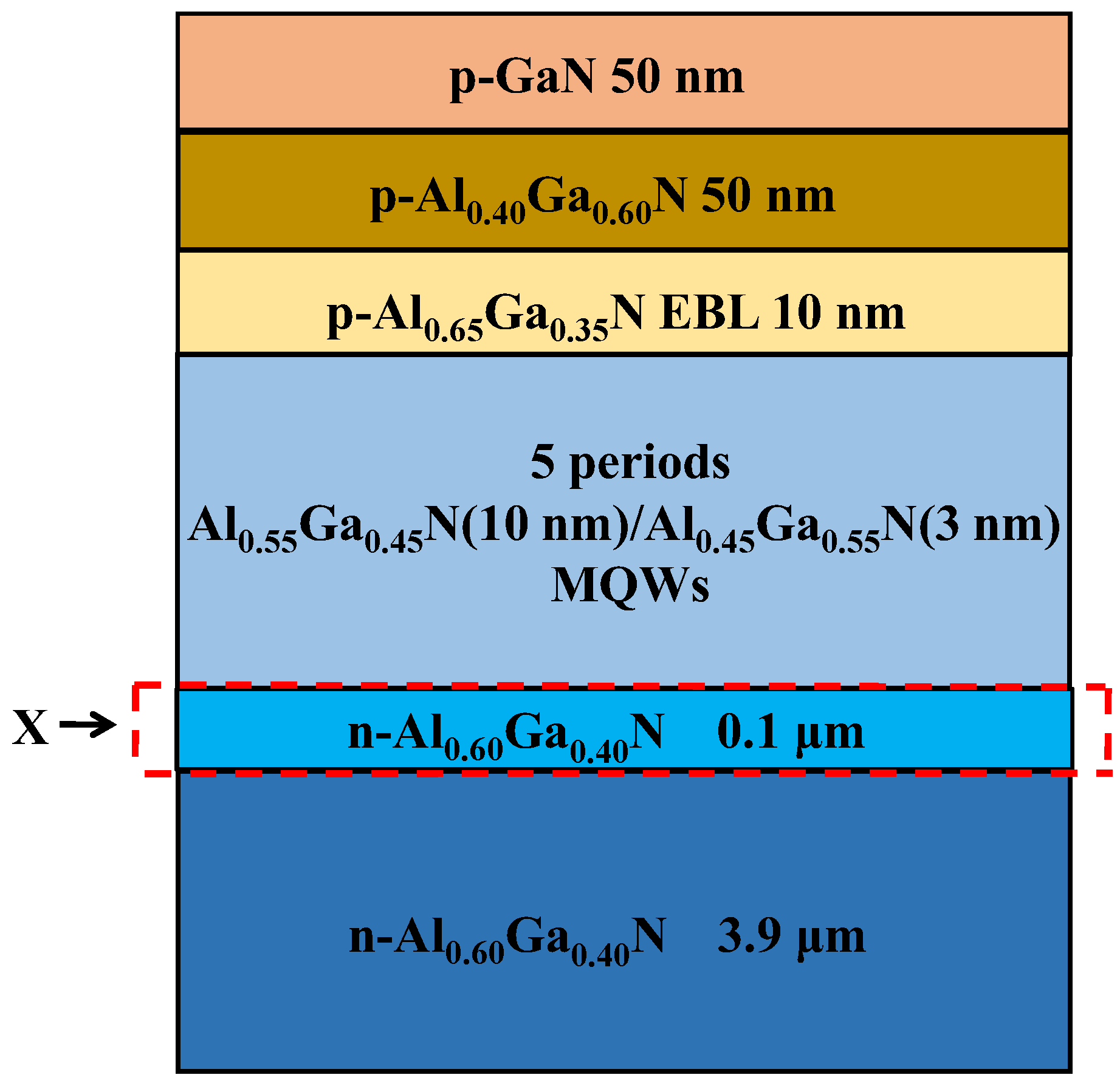
Abstract
:1. Introduction
2. Structures and Parameters
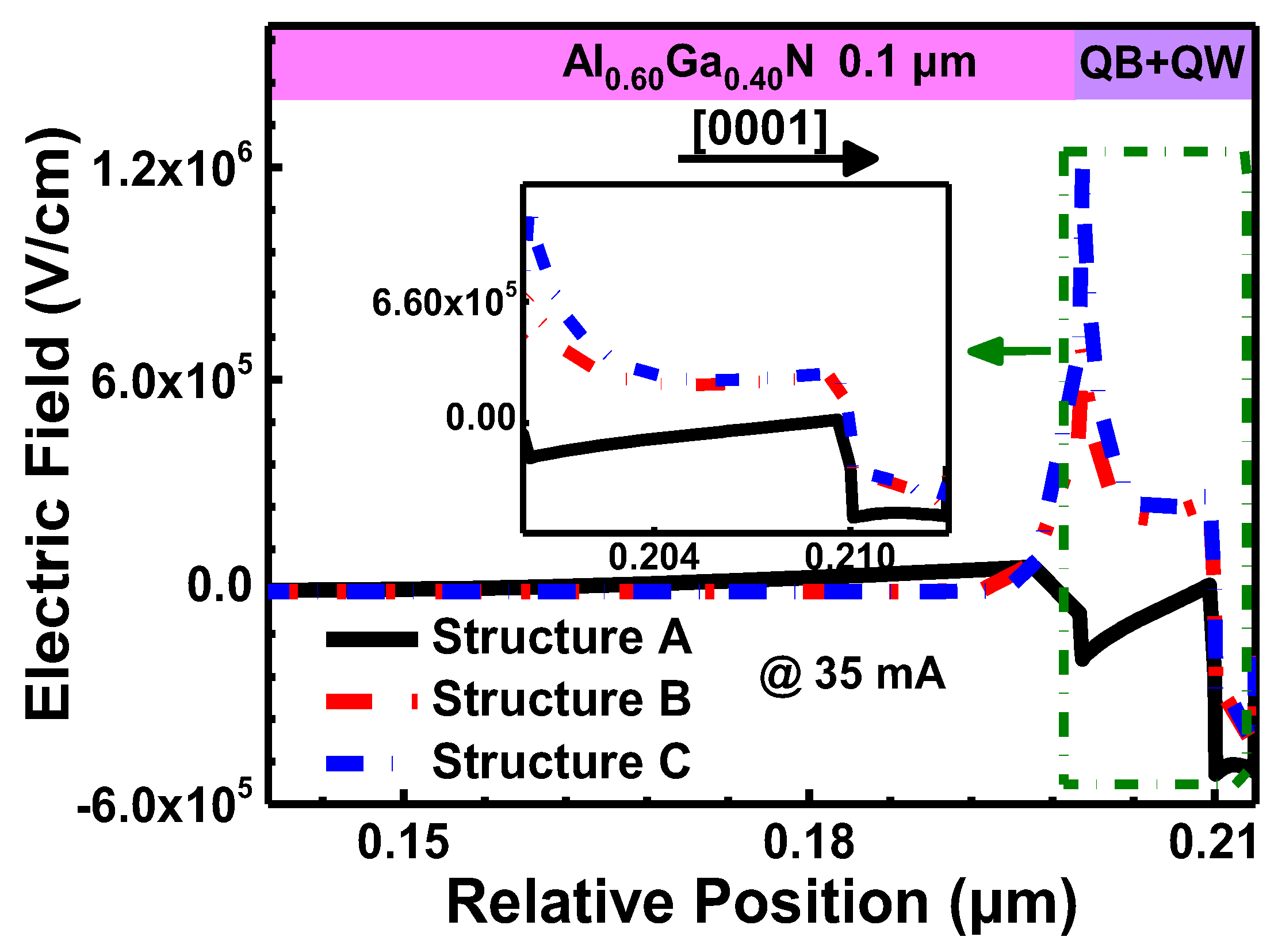
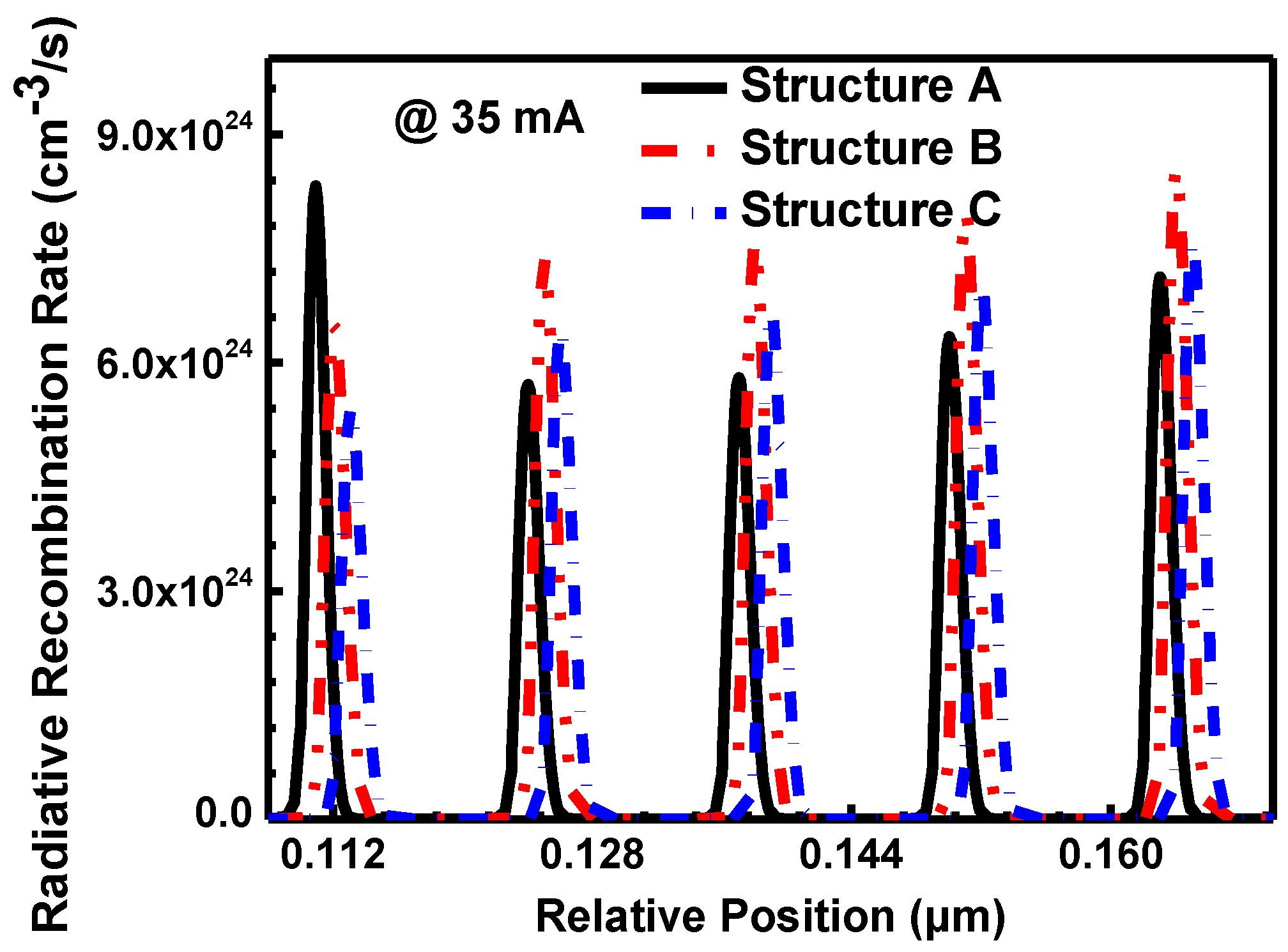
3. Results and Discussions
4. Conclusions
Author Contributions
Funding
Conflicts of Interest
References
- Kneissl, M. A Brief Review of III-Nitride UV Emitter Technologies and Their Application; Springer International Publishing: Cham, Switzerland, 2015; Volume 227, pp. 1–25. [Google Scholar]
- Sun, J.; Sun, H.; Yi, X.; Yang, X.; Liu, T.; Wang, X.; Zhang, X.; Fan, X.; Zhang, Z.; Guo, Z. Efficiency enhancement in AlGaN deep ultraviolet light emitting diodes by adjusting Mg doped staggered barriers. Superlattices Microstruct. 2017, 107, 49–55. [Google Scholar] [CrossRef]
- Ji, X.; Yan, J.; Guo, Y.; Sun, L.; Wei, T.; Zhang, Y.; Wang, J.; Yang, F.; Li, J. Tailoring of Energy Band in Electron-Blocking Structure Enhancing the Efficiency of AlGaN-based Deep Ultraviolet Light-Emitting Diodes. IEEE Photonics J. 2016, 8, 1600607. [Google Scholar] [CrossRef]
- Zhang, Z.-H.; Ju, Z.; Liu, W.; Tan, S.T.; Ji, Y.; Kyaw, Z.; Zhang, X.; Hasanov, N.; Sun, X.W.; Demir, H.V. Improving hole injection efficiency by manipulating the hole transport mechanism through p-type electron blocking layer engineering. Opt. Lett. 2014, 39, 2483–2486. [Google Scholar] [CrossRef] [PubMed] [Green Version]
- Ji, Y.; Zhang, Z.-H.; Tan, S.T.; Ju, Z.G.; Kyaw, Z.; Hasanov, N.; Liu, W.; Sun, X.W.; Demir, H.V. Enhanced hole transport in InGaN/GaN multiple quantum well light-emitting diodes with a p-type doped quantum barrier. Opt. Lett. 2013, 38, 202–204. [Google Scholar] [CrossRef] [PubMed] [Green Version]
- Zhang, Y.; Yu, L.; Li, K.; Pi, H.; Diao, J.; Wang, X.; Shen, Y.; Zhang, C.; Hu, W.; Song, W.; et al. The improvement of deep-ultraviolet light-emitting diodes with gradually decreasing Al content in AlGaN electron blocking layers. Superlattices Microstruct. 2015, 82, 151–157. [Google Scholar] [CrossRef]
- Huang, J.; Guo, Z.; Guo, M.; Liu, Y.; Yao, S.; Sun, J.; Sun, H. Study of Deep Ultraviolet Light-Emitting Diodes with a p-AlInN/AlGaN Superlattice Electron-Blocking Layer. J. Electron. Mater. 2017, 46, 4527–4531. [Google Scholar] [CrossRef]
- Kuo, Y.-K.; Chen, F.-M.; Lin, B.-C.; Chang, J.-Y.; Shih, Y.-H.; Kuo, H.-C. Simulation and Experimental Study on Barrier Thickness of Superlattice Electron Blocking Layer in Near-Ultraviolet Light-Emitting Diodes. IEEE J. Quantum Electron. 2016, 52, 3300306. [Google Scholar] [CrossRef]
- Lin, Y.-Y.; Chuang, R.W.; Chang, S.-J.; Li, S.; Jiao, Z.-Y.; Ko, T.-K.; Hon, S.J.; Liu, C.H. GaN-Based LEDs with a Chirped Multiquantum Barrier Structure. IEEE Photonics Technol. Lett. 2012, 24, 1600–1602. [Google Scholar] [CrossRef]
- Tsai, M.-C.; Yen, S.-H.; Kuo, Y.-K. Deep-ultraviolet light-emitting diodes with gradually increased barrier thicknesses from n-layers to p-layers. Appl. Phys. Lett. 2011, 98, 111114. [Google Scholar] [CrossRef]
- Bao, X.; Sun, P.; Liu, S.; Ye, C.; Li, S.; Kang, J. Performance improvements for AlGaN-based deep ultraviolet light-emitting diodes with the p-type and thickened last quantum barrier. IEEE Photonics J. 2015, 7, 1400110. [Google Scholar] [CrossRef]
- Guo, W.; Xu, F.; Sun, Y.; Lu, L.; Qin, Z.; Yu, T.; Wang, X.; Shen, B. Performance improvement of AlGaN-based deep-ultraviolet light-emitting diodes by inserting single spike barriers. Superlattices Microstruct. 2016, 100, 941–946. [Google Scholar] [CrossRef]
- Zhang, Z.-H.; Liu, W.; Tan, S.T.; Ju, Z.; Ji, Y.; Kyaw, Z.; Zhang, X.; Hasanov, N.; Zhu, B.; Lu, S.; et al. On the mechanisms of InGaN electron cooler in InGaN/GaN light-emitting diodes. Opt. Express 2014, 22, A779–A789. [Google Scholar] [CrossRef] [PubMed] [Green Version]
- Zhang, Z.-H.; Ji, Y.; Liu, W.; Tan, S.T.; Kyaw, Z.; Ju, Z.; Zhang, X.; Hasanov, N.; Lu, S.; Zhang, Y.; et al. On the origin of the electron blocking effect by an n-type AlGaN electron blocking layer. Appl. Phys. Lett. 2014, 104, 073511. [Google Scholar] [CrossRef] [Green Version]
- Tian, K.; Chen, Q.; Chu, C.; Fang, M.; Li, L.; Zhang, Y.; Bi, W.; Chen, C.; Zhang, Z.-H.; Dai, J. Investigations on AlGaN-based deep-ultraviolet light-emitting diodes with Si-doped quantum barriers of different doping concentrations. Phys. Status Solidi 2018, 12, 1700346. [Google Scholar] [CrossRef]
- Ryu, H.-Y.; Jeon, K.-S.; Kang, M.-G.; Choi, Y.; Lee, J.-S. Dependence of efficiencies in GaN-based vertical blue light-emitting diodes on the thickness and doping concentration of the n-GaN layer. Opt. Express 2013, 21, A190–A200. [Google Scholar] [CrossRef] [PubMed]
- Lee, J.-H.; Han, S.-H.; Song, K.-R.; Lee, S.-N. Optical and electrical improvements of semipolar (11-22) GaN-based light emitting diodes by Si doping of n-GaN template. J. Alloys Compd. 2014, 598, 85. [Google Scholar] [CrossRef]
- Fiorentini, V.; Bernardini, F.; Ambacher, O. Evidence for nonlinear macroscopic polarization in III–V nitride alloy heterostructures. Appl. Phys. Lett. 2002, 80, 1204–1206. [Google Scholar] [CrossRef]
- Kuo, Y.-K.; Chang, J.-Y.; Chen, F.-M.; Shih, Y.-H.; Chang, H.-T. Numerical Investigation on the Carrier Transport Characteristics of AlGaN Deep-UV Light-Emitting Diodes. IEEE J. Quantum Electron. 2016, 52, 3300105. [Google Scholar] [CrossRef]
- Piprek, J. Efficiency droop in nitride-based light-emitting diodes. Phys. Status Solidi 2010, 207, 2217–2225. [Google Scholar] [CrossRef]
- Schubert, E.F. Light-Emitting Diodes; Cambridge University Press: Cambridge, UK, 2006; p. 104. ISBN 9780521865388. [Google Scholar]
- Hang, D.R.; Liang, C.-T.; Huang, C.F.; Chang, Y.H.; Chen, Y.F.; Jiang, H.X.; Lin, J.Y. Effective mass of two-dimensional electron gas in an Al0.2Ga0.8N/GaN heterojunction. Appl. Phys. Lett. 2001, 79, 66–68. [Google Scholar] [CrossRef]
- Vurgaftman, I.; Meyer, J.R. Band parameters for nitrogen-containing semiconductors. J. Appl. Phys. 2003, 94, 3675. [Google Scholar] [CrossRef]


© 2018 by the authors. Licensee MDPI, Basel, Switzerland. This article is an open access article distributed under the terms and conditions of the Creative Commons Attribution (CC BY) license (http://creativecommons.org/licenses/by/4.0/).
Share and Cite
Fang, M.; Tian, K.; Chu, C.; Zhang, Y.; Zhang, Z.-H.; Bi, W. Manipulation of Si Doping Concentration for Modification of the Electric Field and Carrier Injection for AlGaN-Based Deep-Ultraviolet Light-Emitting Diodes. Crystals 2018, 8, 258. https://doi.org/10.3390/cryst8060258
Fang M, Tian K, Chu C, Zhang Y, Zhang Z-H, Bi W. Manipulation of Si Doping Concentration for Modification of the Electric Field and Carrier Injection for AlGaN-Based Deep-Ultraviolet Light-Emitting Diodes. Crystals. 2018; 8(6):258. https://doi.org/10.3390/cryst8060258
Chicago/Turabian StyleFang, Mengqian, Kangkai Tian, Chunshuang Chu, Yonghui Zhang, Zi-Hui Zhang, and Wengang Bi. 2018. "Manipulation of Si Doping Concentration for Modification of the Electric Field and Carrier Injection for AlGaN-Based Deep-Ultraviolet Light-Emitting Diodes" Crystals 8, no. 6: 258. https://doi.org/10.3390/cryst8060258