Effect of Substrate Surface on Deposition of AlGaN: A Molecular Dynamics Simulation

1
School of Mechanical Science & Engineering, Huazhong University of Science & Technology, Wuhan 430074, China
2
School of Mechanical & Electronic Engineering, Wuhan University of Technology, Wuhan 430070, China
3
School of Power and Mechanical Engineering, Wuhan University, Wuhan 430072, China
4
School of Science, China University of Geosciences, Beijing 100083, China
*
Authors to whom correspondence should be addressed.
Crystals 2018, 8(7), 279; https://doi.org/10.3390/cryst8070279
Submission received: 22 May 2018
/
Revised: 23 June 2018
/
Accepted: 24 June 2018
/
Published: 3 July 2018
Abstract
:The growth of AlGaN has been extensively studied, but corresponding research related to the effect of AlN substrate surface has rarely been reported in literature. In this article, the effects of AlN substrate surface on deposition of AlGaN films were investigated by molecular dynamics (MD) simulations. (0001) Al-terminated and N-terminated AlN were considered as substrates. The quality of surface morphology and atomic scale structure of deposited AlGaN film are discussed in detail. The results show that the surface morphology and crystal quality of AlGaN film grown on (0001) Al-terminated AlN surface are better than for that grown on N-terminated AlN surface under various growing temperatures and Al/Ga injection ratios between Al and Ga. This can be attributed to the higher mobility of Al and Ga adatoms on the (0001) Al-terminated AlN surface. These findings can provide guidance for the preparation of high-quality AlGaN thin films on AlN substrate.

1. Introduction
III-Nitrides have attracted much attention over the past decades due to their excellent optoelectronic and physical properties [1,2,3]. Benefitting from an adjustable band gap (3.4 eV to 6.2 eV), AlGaN alloys are widely used in the area of optical devices such as laser diodes (LDs) [4], light emitting diodes (LEDs) [5] and photodetectors [6]. Especially in deep ultraviolet LED (DUV-LEDs), AlGaN/AlN superlattices (SLs) are used for filtering dislocations and relieving stresses [7]. Moreover, it is applied in n and p electrodes as the container of negative and positive carriers, respectively [8,9]. In addition, it is a component of multiple quantum wells (MQWs), which serve as the active region for the recombination of carriers [10].
The growth of AlGaN film has been extensively studied for its wide application and AlN often serves as the buffer layer for growing AlGaN due to the small lattice mismatch between them [11]. So far, the growth of AlGaN film on AlN buffer layers has mainly been investigated by experimental studies. Growing temperature [12], pressure [13], Al concentration [14] and V/III ratio [15] during the growth of AlGaN film have been frequently investigated. However, little attention has been paid to exploring the effect of the AlN surface on the growth of AlGaN film, while the GaN surface has been systematically studied [16,17]. Moreover, characters such as surface morphology, atomic structure, defects and migration process during the growth process can be visualized directly by MD simulations instead of experiments. These characteristics provide fundamental and principal understanding of the growth process, and may guide the practical experiments.
Recently, MD simulation has been extensively employed to systematically investigate the growth of III-V binary [18,19] and ternary compounds [20,21]. The growth of GaN on polar surfaces [18] and AlN on non-polar surfaces [19] were investigated; additionally, the growth of ternary InGaN film on polar [20] and non-polar [21] GaN surfaces was also discussed. The formation of defects on these planes was explored.
However, MD simulation of AlGaN film grown on AlN has rarely been reported, particularly with regard to the substrate surface effect. AlN is typically grown along the c-plane [22,23]. C-plane AlN has two kinds of polarities ((0001) and ) and two kinds of terminal surfaces (Al-terminated and N-terminated surfaces), resulting in four combinations: (0001) Al-terminated, (0001) N-terminated, Al-terminated and N-terminated AlN. In this paper, we chose two of them—the (0001) Al-terminated and N-terminated AlN surfaces—to analyze the effect of the substrate surface on the growth of AlGaN film. AlGaN films with different growth temperatures and injected Al concentrations were deposited. The surface morphology and atomic structures are discussed in detail. Furthermore, the migration process of adatoms is compared.
2. Calculation Methods
2.1. Interatomic Potential
The Large-scale Atomic/Molecular Massively Parallel Simulator (LAMMPS) [24] with SW potential [25,26] has been adopted. So far, there have been many potentials developed for GaN [27,28,29] and AlN [30,31], but few potentials describe the interatomic potentials of Al-Ga-N. In this work, the SW potential is chosen to describe the interatomic interaction in Al-Ga-N. It can accurately characterize the elastic, structural and dynamical properties of AlN and GaN, and can well describe the interatomic interaction between Al-Ga. Similar SW potentials have already been successfully applied to investigate InGaN film grown on GaN surface [20,21]. The parameters of Al-Ga-N SW potential are shown in Table 1. More details can be found in References [25,26]. And the SW potential file are uploaded as Supplementary Material.
2.2. Simulation Details
The 3D model of the AlN substrate is shown in Figure 1a, x, y and z represent the directions , and (0001) (or ), respectively. The AlN substrate consists of 5400 Al atoms and 5400 N atoms with Al-terminated plane (shown in Figure 1b) or with N-terminated plane along the z axis (shown in Figure 1c). The specific data files have been uploaded as Supplementary Materials. The AlN substrate is divided into three groups: two pairs of atoms at the bottom of the substrate make up the fixed group to prevent movement of the substrate due to the deposition of atoms. Two pairs of atoms on the top of the substrate constitute the free group, in which the atoms are entirely free to interact and transmit energy with the deposited atoms. The rest of the atoms in the middle of the substrate act as the thermal control group, where the NVT ensemble is used to perform time integration on Nose-Hoover style non-Hamiltonian equations of motion to update the positions and velocities of the atoms to obtain the prescribed substrate temperature. Periodic boundary conditions (PBCs) are applied in the x and y directions to create a seemingly infinite boundary, while a free boundary condition (FBC) is applied to the z direction to enable the deposition of Al, Ga and N atoms. The growth of AlGaN is simulated by periodically injecting an Al atom, a Ga atom or a N atom from a 25-fold lattice height toward the AlN substrate surface with an incident angle of 0° (perpendicular to the substrate), which is indicated by the black arrow in Figure 1. The injected atoms are all assigned a kinetic energy of 0.17 eV [18]. The time interval of injected N atoms is kept at a constant 2.5 ps per atom, and the total number of injected N atoms is 8000. Meanwhile, the time interval and number of injected Al and Ga atoms are varied to get different injected Al:Ga ratios, but the injected (Al + Ga):N ratio remains 1 under all conditions. The deposition process takes 20,000 ps. After the deposition, a relaxation process of 5000 ps is carried out to equilibrate the system.
2.3. Analysis Methods
The visualization is realized using the open visualization tool (OVITO) [32]. Identify diamond structure (IDS) [33] in OVITO is used to identify the atoms arranged in hexagonal (wurtzite) or cubic diamond (zinc blende) lattice. The algorithm analyzes the local environment of each atom up to the second neighbor shell to determine the local structural type. To classify a central atom, the second nearest neighbors are taken into account to discriminate between cubic and hexagonal diamond structures. This method involves the characterization of the geometrical arrangement of the second nearest neighbors.
3. Results and Discussion
3.1. Surface Morphology
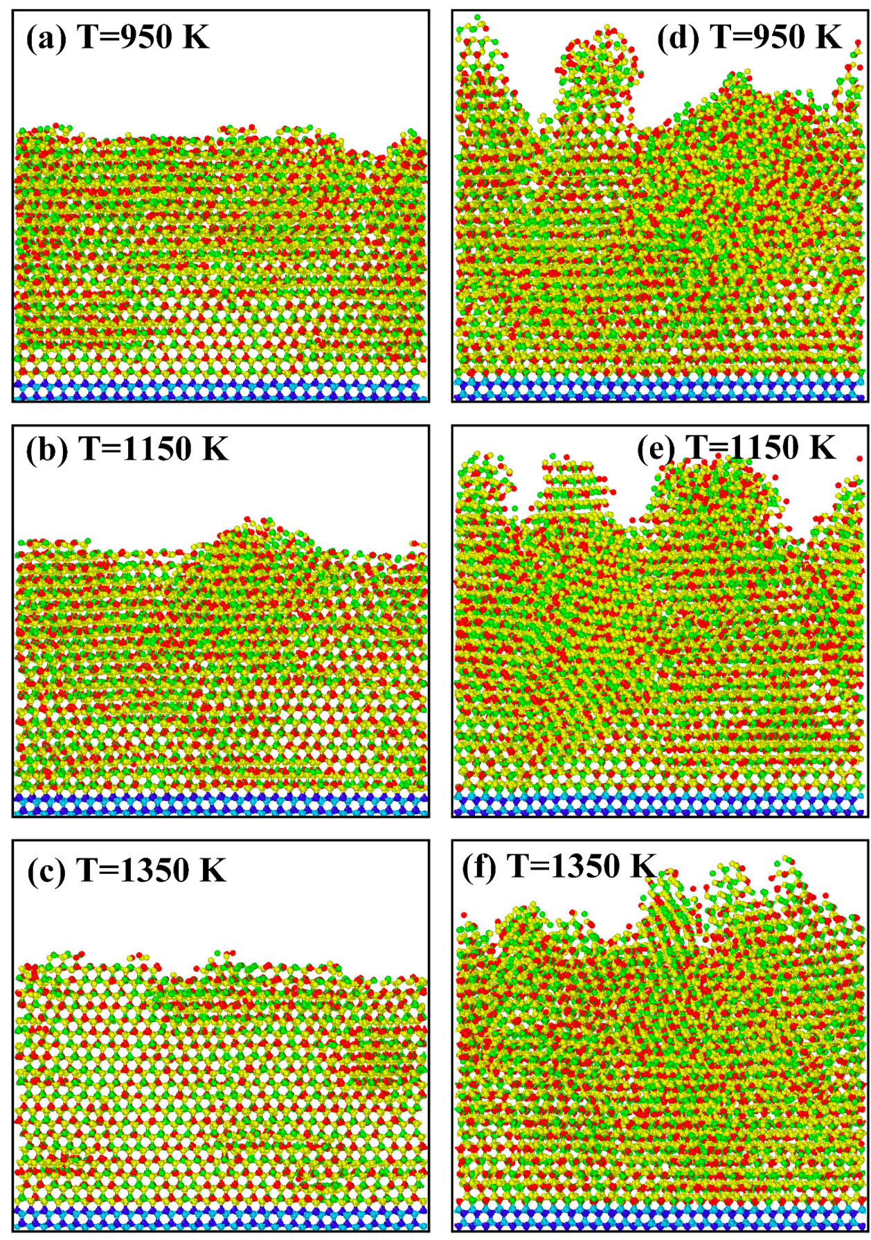
A smooth surface is a critical indicator of high-quality AlGaN film. Figure 2 shows the surface evolution process of deposited AlGaN films on two different terminal surfaces at 1350 K with injected Al:Ga ratio = 3:5. Four snapshots are presented to describe the growth process. At the initial stage of growth (t = 5000 ps), Al, Ga, and N atoms are injected toward the AlN substrate and bond to each other, then they overspread the substrates as shown in Figure 2a,e. A smoother surface is observed in Figure 2a than in Figure 2e, although the distinction is ambiguous. As the deposition continues, the AlGaN films grow thicker as shown in Figure 2b,c,f,g. Relatively smooth surfaces can still be observed in Figure 2b,c. Compared to Figure 2b, Figure 2f shows island-like structures on the surface, and the island structures are strengthened in Figure 2g. At the final deposition stage, Figure 2d still shows a comparatively 2D surface, while a deteriorated 3D surface is observed in Figure 2h. We find that adatoms are more likely to find an ideal lattice site before the impacting of other atoms when grown on the (0001) Al-terminated surface, so a smooth film surface is achieved. In contrast, when growing on the N-terminated surface, adatoms are less able to move away from their initial deposited positions, and the subsequently impacting atoms soon bury the deposited atoms before they move. Consequently, the 3D growth mode is formed.
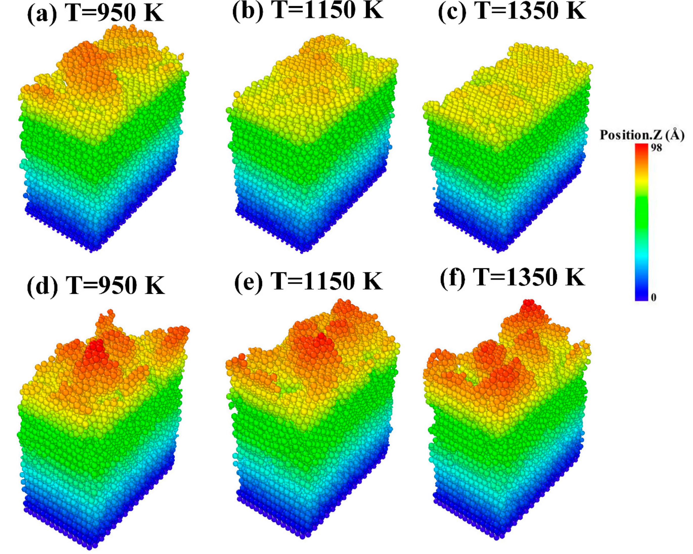
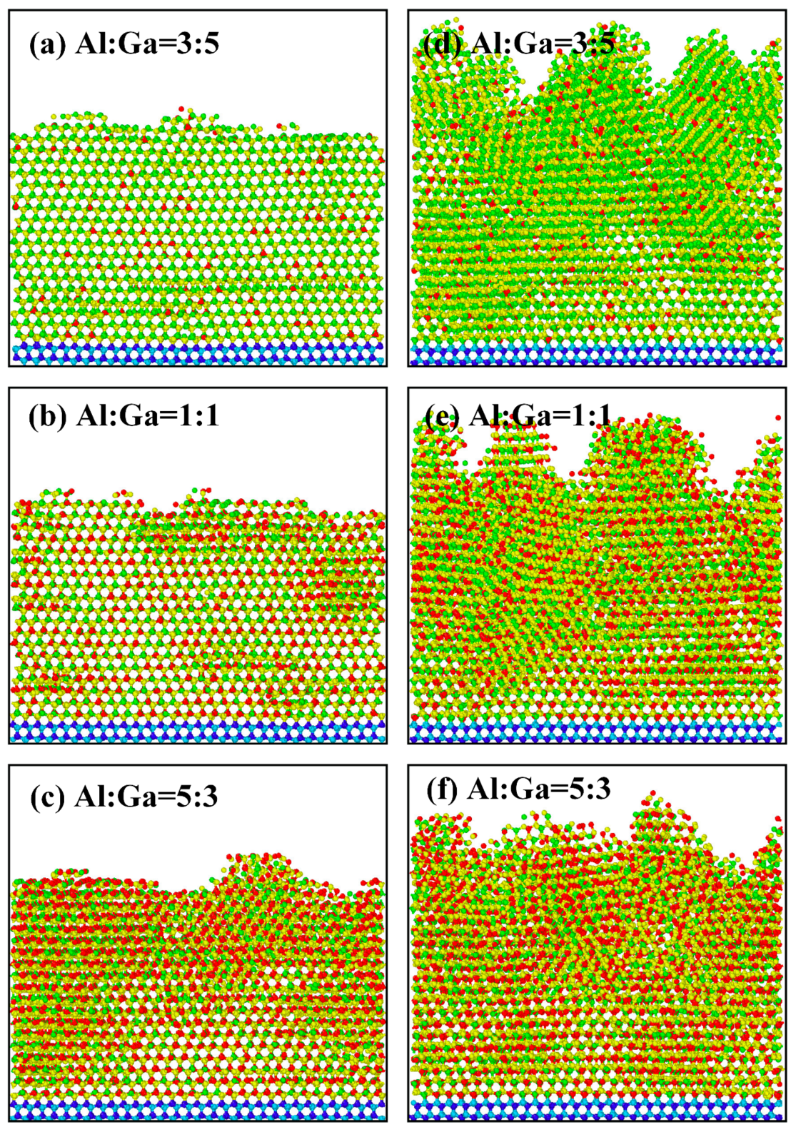
To further explore the surface morphology of AlGaN film on two different AlN substrates, the surface morphology of the deposited AlGaN films grown on AlN substrates after relaxation is shown in Figure 3 and Figure 4, in which the atoms are colored by height along the z axis. Figure 3 shows the surface morphology of the deposited AlGaN film under different temperatures and substrate surfaces. From Figure 3, we easily find that when growing on the N-terminated surface, AlGaN films show a rough surface under all temperatures. On the other hand, AlGaN films exhibit a smooth surface when growing on the (0001) Al-terminated surface. Moreover, the surface gets smoother when the temperature increases from 950 K to 1350 K.
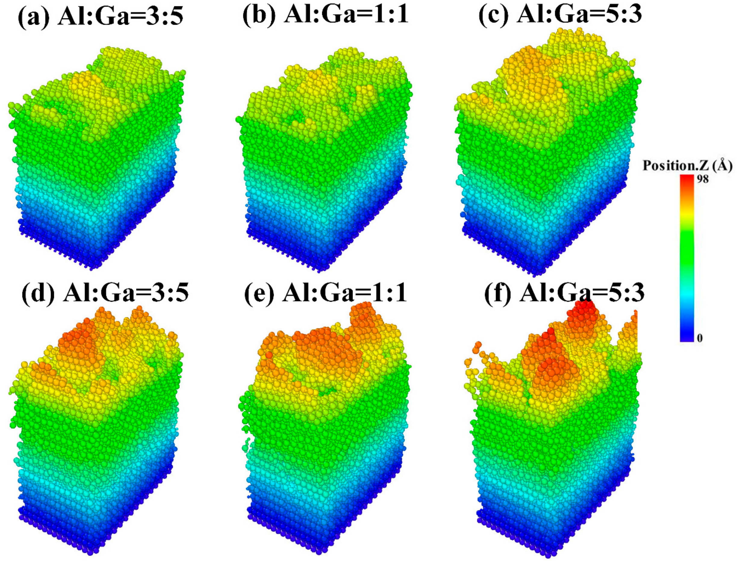
Figure 4 shows the surface morphology of the deposited AlGaN film under different injected Al:Ga ratios and substrate surfaces at 1250 K. It is obvious that AlGaN film grown on (0001) Al-terminated surface exhibits a relatively smooth surface and displays a rough surface on the N-terminated surface under all injected Al:Ga ratios. In addition, the surface gets rougher when increasing the injected Al:Ga ratio on the (0001) Al-terminated surface. The fact that at low Al contents, Ga adatoms with high surface mobility dominate the growth mechanisms, leading to smooth surface morphologies, has also been proven by experiment [34].
Taken together, AlGaN film grown on the (0001) Al-terminated surface has much better surface morphology than that grown on the N-terminated surface. The growth mode of AlGaN on the (0001) Al-terminated surface trends towards a 2D mode, while that on N-terminated surface trends towards 3D.
3.2. Atomic Structure
Crystal lattice perfection is essential for AlGaN film. Deviation from ideal lattice configuration can change the coordinates of atoms and overstretch bonds, resulting in changed electron populations in the valence and conduction bands. In addition, the existence of defects and even polytypism seriously affects the electrical and optical properties of AlGaN [35]. Thus, high-quality AlGaN film with low lattice deformation and low defect concentration is required for such applications.
The atomic arrangement of the deposited AlGaN films at 950K, 1150 K and 1350 K with injected Al:Ga ratio of 1:1 are investigated to explore lattice perfection, as shown in Figure 5. For a perfect lattice, the hexagonal mesh structure can be observed when looking along the x axis, as the substrate atoms show. When growing on the (0001) Al-terminated AlN surface (shown in Figure 5a–c), the deposited atoms are arranged in a very orderly fashion; the regular pattern of the deposited atoms can still be observed. Meanwhile, we can also see there are lattice distortions due to the deviation from the ideal lattice sites of some atoms. However, the overall atomic arrangement is orderly. The hexagonal mesh structure can be observed in most parts of the deposited film. In general, the overall arrangement of deposited atoms is comparatively good. Compared with Figure 5a–c, the deposited atoms in Figure 5d–f are much more disordered. Many atoms pile up together, while some other atoms loosely bond with each other, leading to massive interstitial atoms and vacancies. The arrangement of atoms can hardly be detected. It is obvious that AlGaN grown on (0001) Al-terminated AlN surface has a better crystal lattice arrangement. Moreover, the arrangement of atoms gets more orderly as the temperature increases from 950 K to 1350 K when growing on (0001) Al-terminated AlN surface.
Figure 6 shows the atomic arrangement of deposited AlGaN films at 1350 K with injected Al:Ga ratio of 3:5, 1:1 and 5:3 at 1350 K under different AlN substrates: (a)–(c) (0001) Al-terminated AlN; (d)–(f) N-terminated AlN. We can easily find that the deposited atoms are in great disorder when growing on N-terminated AlN surface under all injected Al:Ga ratios. When growing on (0001) Al-terminated AlN, the arrangement of deposited atoms is relatively good and gets a little worse as the injected Al:Ga ratio increases from 3:5 to 5:3.
Generally, better surface morphology and atomic scale structure of AlGaN film is achieved when grown on (0001) Al-terminated than on N-terminated AlN. When increasing the temperature from 950 K to 1350 K, the surface morphology and atomic scale structure of AlGaN film grown on (0001) Al-terminated surface get better. This is due to the increased mobility of deposited atoms as the temperature increases [36], which facilitates the deposited atoms finding their ideal lattice sites. Increasing temperature improves the surface morphology and atomic scale structure of deposited AlGaN film. The surface morphology and atomic scale structure of AlGaN film grown on (0001) Al-terminated surface deteriorate as the injected Al:Ga ratio increases from 3:5 to 5:3, because the mobility of Al atoms is lower than that of Ga atoms [37]; it is more difficult for Al atom to move than for Ga atom. The low surface mobility of Al atoms prevents Al atoms from finding the ideal lattice site, which leads to bad surface morphology and atomic scale structure. Thus, increasing the injected Al:Ga ratio degrades the surface morphology and atomic scale structure of deposited AlGaN film.
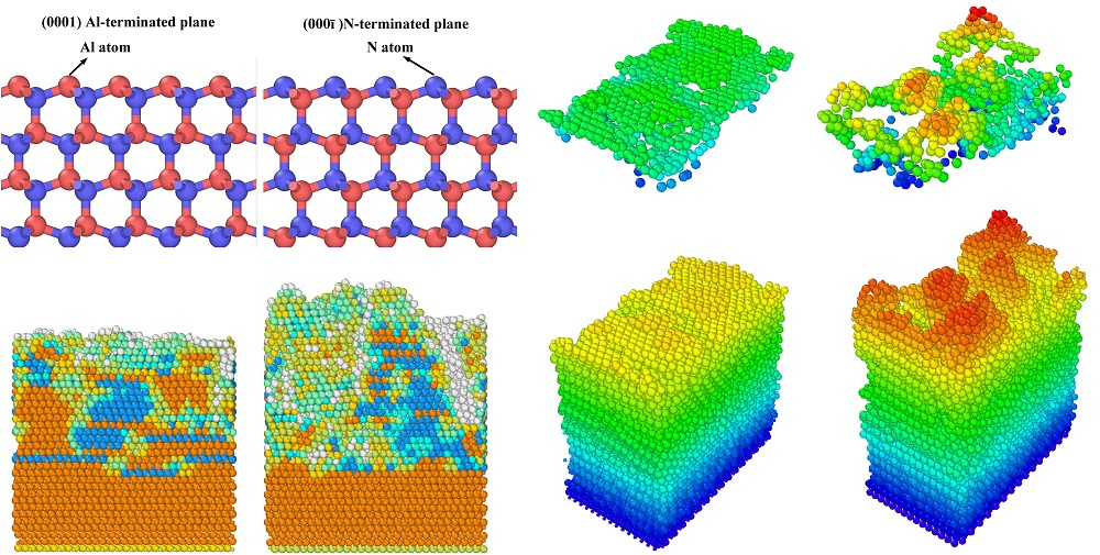
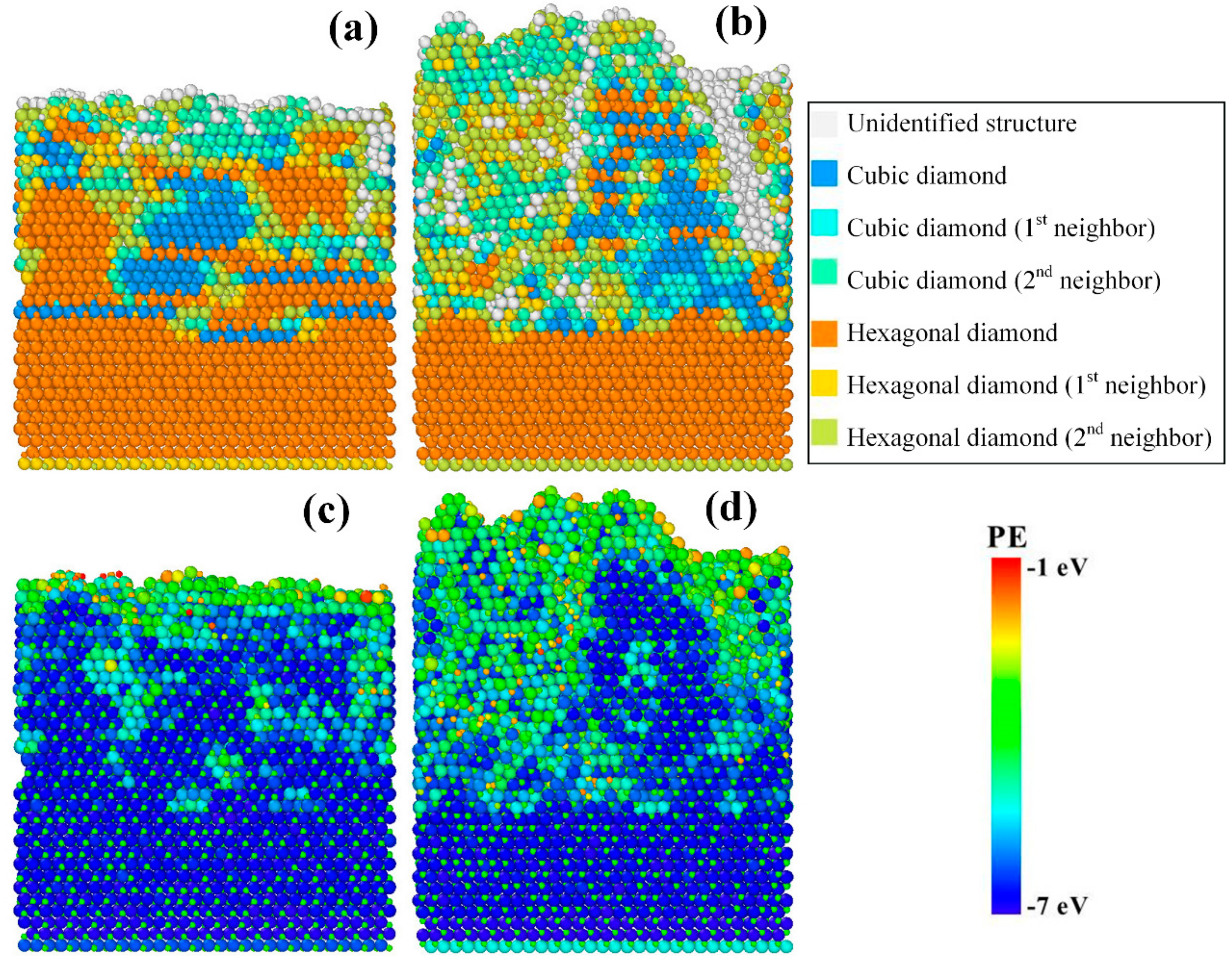
The atomic structures of deposited AlGaN film at 1150 K on two different terminal surfaces are further investigated, and the structural constituent and corresponding distribution of potential energy (PE) is shown in Figure 7. In order to show more clearly the defect region, the local lattice structures are indicated by colors. From Figure 7a,b, we find that there are more hexagonal (wurtzite) structures in AlGaN grown on (0001) Al-terminated surface, while more US (unidentified structures) are found in AlGaN grown on N-terminated AlN surface. In addition, we can see that there are cubic diamonds (zinc blende) in both Figure 7a,b. The wurtzite and zinc blende structures appear alternately along the film thickness direction, bounded horizontally by stacking faults. This may be exaggerated because the energy differences between wurtzite and zinc blende are both small for AlN and GaN [38], and the SW potential ensures the lowest energies for the equilibrium wurtzite and zinc blende phase for both AlN and GaN. In general, AlGaN grown on (0001) Al-terminated AlN surface has a better atomic structure than that grown on N-terminated AlN surface. Comparing Figure 7a,c, we find that PE in the region of the defects is higher than that in the region with the ideal lattice structure, which is in accordance with the theoretical calculation [39]. The correspondence between defects and PE distribution provides us with another method to locate defects.
3.3. Atomic Migration Mechanisms
Taking the above results into consideration, we can easily find that (0001) Al-terminated AlN is a better template for growing AlGaN to get better surface morphology and crystal quality. Because Al and Ga adatoms have lower diffusion barriers on (0001) Al-terminated than on terminated [36]. This means that Al and Ga adatoms are more mobile on (0001) Al-terminated AlN surface than on AlN N-terminated surface, which facilitates the movement for Al and Ga adatoms to find the ideal lattice site. As a result, better surface morphology and crystal quality are expected. (0001) Al-terminated surface substantially improves the surface roughness and crystal quality of deposited AlGaN film. Similarly, J. Gruber et al. chose (0001) Ga-terminated GaN template for the growth of InGaN [20]. Ponce et al. [40] examined smooth MOCVD films grown on sapphire with a low-temperature GaN buffer layer and reported them to be (0001) Ga-polar. Rouvière et al. [41] studied MOCVD films with various growth conditions. They reported that the smooth films typically obtained with a low temperature buffer layer are predominantly Ga-polar. Meanwhile M. Sumiya [42] and M. Stutzmann [43] proved that Ga-polar GaN surface is the surface of choice for growing III-Nitrides and its related applications. They are all consistent with our study here.
To further verify the different mobility of Al and Ga adatoms on two different surfaces, the time-resolved processes for migration of adatoms on the substrate surfaces at 1450 K and injected Al:Ga = 1:1 are displayed in Figure 8. Figure 8a–d shows the migration process of adatoms on (0001) Al-terminated AlN surface, while Figure 8e–h shows the migration process of adatoms on N-terminated AlN surface. In Figure 8a,b, the adatoms successively approach the substrate then start to bond with appropriate atoms. We can see in Figure 6c that the N adatom bonds with Al atom on the substrate and another N adatom moves toward the Al adatoms. The next moment, in Figure 8d, the bond between the first N adatom and substrate Al atom breaks up and the N adatom moves toward the Ga adatom to find a new lattice site. Meanwhile, another pair of Al and N adatoms also move towards each other. A similar process can be observed in Figure 8e–h. However, when we carefully compare the migration processes on different surfaces, we find that Al and Ga adatoms gradually move away from their initial position after they approach the (0001) Al-terminated surface. By comparison, Al and Ga adatoms have little movement from their initial position after they approach the N-terminated surface. Apparently, Al and Ga adatoms have a longer migration length on (0001) Al-terminated AlN surface than on N-terminated AlN surface, facilitating the movement of Al and Ga adatoms to find the ideal lattice site.
4. Conclusions
We have studied the effect of substrate surface on the deposition of AlGaN film on two AlN surfaces: (0001) Al-terminated and N-terminated AlN surface. Growth temperatures and injected Al:Ga ratios were varied to comprehensively explore the effects. The surface morphology and atomic structure of deposited AlGaN film were discussed in detail. The results show that AlGaN film grown on (0001) Al-terminated surface has better surface morphology and crystal quality than that grown on N-terminated surface under all conditions. The reason was further explored, and we find that Al and Ga adatoms are more mobile on (0001) Al-terminated surface, which facilitates the movement of Al and Ga adatoms to find their ideal lattice sites. Thus, better surface morphology and crystal structure are expected. In addition, when growing on (0001) Al-terminated AlN surface, AlGaN film shows the better surface morphology and atomic scale structure as the temperature increases from 950 K to 1350 K. The surface morphology and atomic scale structure deteriorate when increasing the injected Al:Ga ratio from 3:5 to 5:3. The result that (0001) Al-terminated AlN is a better candidate for growth of AlGaN film agrees well with previous theoretical research. Furthermore, our simulation suggests that MD simulation offers new possibilities to probe into the growth process and mechanisms of AlGaN alloy. Based on the results obtained, we foresee further practical study on the growth of AlGaN film.
Supplementary Materials
The datasets supporting this article have been uploaded as part of the Supplementary Material.
Author Contributions
Conceptualization, L.Z. and Z.G.; Data curation, H.Y. and G.Z.; Funding acquisition, S.L. and Z.G.; Investigation, G.Z.; Methodology, L.Z. and H.Y.; Project administration, Z.G.; Resources, Z.G. and Z.Z.; Software, L.Z.; Supervision, H.Y. and Z.G.; Validation, S.L., Z.G. and Z.Z.; Visualization, L.Z.; Writing—original draft, L.Z. and H.Y.; Writing—review & editing, L.Z. and Z.G.
Funding
This research was funded by the National Natural Science Foundation of China under grant number 51727901, 51476068 and 51402224.
Acknowledgments
The work was carried out at National Supercomputer Center in Tianjin, and the calculations were performed on TianHe-1(A).
Conflicts of Interest
The authors declare no conflict of interest.
References
- Zhang, J.P.; Wang, H.M.; Gaevski, M.E.; Chen, C.Q.; Fareed, Q.; Yang, J.W.; Simin, G.; Khan, M.A. Crack-free thick AlGaN grown on sapphire using AlN/AlGaN superlattices for strain management. Appl. Phys. Lett. 2002, 80, 3542–3544. [Google Scholar] [CrossRef] [Green Version]
- Xiang, H.G.; Li, H.T.; Fu, T.; Zhao, Y.B.; Huang, C.; Zhang, G.; Peng, X.H. Molecular dynamics simulation of AlN thin films under nanoindentation. Ceram. Int. 2017, 43, 4068–4075. [Google Scholar] [CrossRef]
- Xiang, H.; Li, H.; Fu, T.; Huang, C.; Peng, X. Formation of prismatic loops in AlN and GaN under nanoindentation. Acta Mater. 2017, 138, 131–139. [Google Scholar] [CrossRef]
- Liang, F.; Zhao, D.-G.; Jiang, D.-S.; Liu, Z.-S.; Zhu, J.-J.; Chen, P.; Yang, J.; Liu, W.; Liu, S.-T.; Xing, Y.; et al. Output light power of InGaN-based violet laser diodes improved by using a u-InGaN/GaN/AlGaN multiple upper waveguide. Chin. Phys. B 2017, 26, 124210. [Google Scholar] [CrossRef] [Green Version]
- Lu, L.; Wan, Z.; Xu, F.J.; Shen, B.; Lv, C.; Jiang, M.; Chen, Q.G. Improving Performance of Algan-Based Deep-Ultraviolet Light-Emitting Diodes by Inserting a Higher Al-Content Algan Layer Within the Multiple Quantum Wells. Phys. Status Solidi A 2017, 214, 1700461. [Google Scholar] [CrossRef]
- Rathkanthiwar, S.; Kalra, A.; Solanke, S.V.; Mohta, N.; Muralidharan, R.; Raghavan, S.; Nath, D.N. Gain mechanism and carrier transport in high responsivity AlGaN-based solar blind metal semiconductor metal photodetectors. J. Appl. Phys 2017, 121, 164502. [Google Scholar] [CrossRef]
- Mastro, M.A.; Eddy, C.R.; Gaskill, D.K.; Bassim, N.D.; Casey, J.; Rosenberg, A.; Holm, R.T.; Henry, R.L.; Twigg, M.E. MOCVD growth of thick AlN and AlGaN superlattice structures on Si substrates. J. Cryst. Growth 2006, 287, 610–614. [Google Scholar] [CrossRef]
- Chichibu, S.F.; Miyake, H.; Ishikawa, Y.; Furusawa, K.; Hiramatsu, K. Spatio-time-resolved cathodoluminescence study on high AlN mole fraction AlxGa1−xN structures grown by metalorganic vapor phase epitaxy. Appl. Phys. Lett. 2015, 107, 121602. [Google Scholar] [CrossRef]
- Wang, L.; Li, R.; Li, D.; Liu, N.; Liu, L.; Chen, W.; Wang, C.; Yang, Z.; Hu, X. Strain modulation-enhanced Mg acceptor activation efficiency of Al0.14Ga0.86N/GaN superlattices with AlN interlayer. Appl. Phys. Lett 2010, 96, 061110. [Google Scholar] [CrossRef]
- Fujioka, A.; Misaki, T.; Murayama, T.; Narukawa, Y.; Mukai, T. Improved Efficiency of 255–280 nm AlGaN-Based Light-Emitting Diodes. Appl. Phys. Express 2010, 3, 061004. [Google Scholar] [CrossRef]
- Susilo, N.; Hagedorn, S.; Jaeger, D.; Miyake, H.; Zeimer, U.; Reich, C.; Neuschulz, B.; Sulmoni, L.; Guttmann, M.; Mehnke, F.; et al. AlGaN-based deep UV LEDs grown on sputtered and high temperature annealed AlN/sapphire. Appl. Phys. Lett. 2018, 112, 041110. [Google Scholar] [CrossRef]
- Koukitu, A.; Seki, H. unstable region of solid composition in ternary nitride alloys grown by metalorganic vapor-phase epitaxy. Jpn. J. Appl. Phys. 1996, 35, L1638–L1640. [Google Scholar] [CrossRef]
- Lu, D.C.; Duan, S. Quasi-thermodynamic analysis of MOVPE of AlGaN. J. Cryst. Growth 2000, 208, 73–78. [Google Scholar] [CrossRef]
- Xi, Y.A.; Chen, K.X.; Mont, F.W.; Kim, J.K.; Lee, W.; Schubert, E.F.; Liu, W.; Li, X.; Smart, J.A. Kinetic study of Al-mole fraction in AlxGa1−xN/AlxGa1−xN grown on c-plane sapphire and AlN bulk substrates by metal-organic vapor-phase epitaxy. Appl. Phys. Lett 2007, 90, 051104. [Google Scholar] [CrossRef]
- Lobanova, A.V.; Mazaev, K.M.; Talalaev, R.A.; Leys, M.; Boeykens, S.; Cheng, K.; Degroote, S. Effect of V/III ratio in AlN and AlGaN MOVPE. J. Cryst. Growth 2006, 287, 601–604. [Google Scholar] [CrossRef]
- Zúñiga-Pérez, J.; Consonni, V.; Lymperakis, L.; Kong, X.; Trampert, A.; Fernández-Garrido, S.; Brandt, O.; Renevier, H.; Keller, S.; Hestroffer, K.; et al. Polarity in GaN and ZnO: Theory, measurement, growth, and devices. Appl. Phys. Rev. 2016, 3, 041303. [Google Scholar] [CrossRef]
- Himmerlich, M.; Lymperakis, L.; Gutt, R.; Lorenz, P.; Neugebauer, J.; Krischok, S. GaN(0001) surface states: Experimental and theoretical fingerprints to identify surface reconstructions. Phys. Rev. B 2013, 88, 125304. [Google Scholar] [CrossRef]
- Zhou, X.W.; Murdick, D.A.; Gillespie, B.; Wadley, H.N.G. Atomic assembly during GaN film growth: Molecular dynamics simulations. Phys. Rev. B 2006, 73, 045337. [Google Scholar] [CrossRef]
- Leathersich, J.; Suvarna, P.; Tungare, M.; Shahedipour-Sandvik, F.S. Homoepitaxial growth of non-polar AlN crystals using molecular dynamics simulations. Surf. Sci. 2013, 617, 36–41. [Google Scholar] [CrossRef]
- Gruber, J.; Zhou, X.W.; Jones, R.E.; Lee, S.R.; Tucker, G.J. Molecular dynamics studies of defect formation during heteroepitaxial growth of InGaN alloys on (0001) GaN surfaces. J. Appl. Phys. 2017, 121, 195301. [Google Scholar] [CrossRef] [PubMed] [Green Version]
- Chu, K.; Gruber, J.; Zhou, X.W.; Jones, R.E.; Lee, S.R.; Tucker, G.J. Molecular dynamics studies of InGaN growth on nonpolar (1120) GaN surfaces. Phys. Rev. Mater. 2018, 2, 013402. [Google Scholar] [CrossRef]
- Bryan, I.; Bryan, Z.; Washiyama, S.; Reddy, P.; Gaddy, B.; Sarkar, B.; Breckenridge, M.H.; Guo, Q.; Bobea, M.; Tweedie, J.; et al. Doping and compensation in Al-rich AlGaN grown on single crystal AlN and sapphire by MOCVD. Appl. Phys. Lett. 2018, 112, 062102. [Google Scholar] [CrossRef] [Green Version]
- Luo, W.; Li, L.; Li, Z.; Yang, Q.; Zhang, D.; Dong, X.; Peng, D.; Pan, L.; Li, C.; Liu, B.; et al. Influence of the nucleation layer morphology on the structural property of AlN films grown on c-plane sapphire by MOCVD. J. Alloys Compd. 2017, 697, 262–267. [Google Scholar] [CrossRef]
- Plimpton, S. Fast Parallel Algorithms for Short-Range Molecular Dynamics. J. Comput. Phys. 1995, 117, 1–19. [Google Scholar] [CrossRef] [Green Version]
- Zhou, X.W.; Jones, R.E.; Kimmer, C.J.; Duda, J.C.; Hopkins, P.E. Relationship of thermal boundary conductance to structure from an analytical model plus molecular dynamics simulations. Phys. Rev. B 2013, 87, 094303. [Google Scholar] [CrossRef]
- Zhou, X.W.; Jones, R.E.; Duda, J.C.; Hopkins, P.E. Molecular dynamics studies of material property effects on thermal boundary conductance. Phys. Chem. Chem. Phys. 2013, 15, 11078–11087. [Google Scholar] [CrossRef] [PubMed]
- Nord, J.; Albe, K.; Erhart, P.; Nordlund, K. Modelling of compound semiconductors: Analytical bond-order potential for gallium, nitrogen and gallium nitride. J. Phys. Condens. Matter 2003, 15, 5649–5662. [Google Scholar]
- Béré, A.; Serra, A. On the atomic structures, mobility and interactions of extended defects in GaN: Dislocations, tilt and twin boundaries. Philos. Mag. 2006, 86, 2159–2192. [Google Scholar] [CrossRef]
- Zhou, X.W.; Foster, M.E.; Jones, R.; Yang, P.; Fan, H.; Doty, F.P. a modified Stillinger-Weber potential for TlBr, and its polymorphic extension. J. Mater. Sci. Res. 2015, 4, 15. [Google Scholar] [CrossRef]
- Tungare, M.; Shi, Y.; Tripathi, N.; Suvarna, P.; Shahedipour-Sandvik, F.S. A Tersoff-based interatomic potential for wurtzite AlN. Phys. Status Solidi A 2011, 208, 1569–1572. [Google Scholar] [CrossRef]
- Vashishta, P.; Kalia, R.K.; Nakano, A.; Rino, J.P. Interaction potential for aluminum nitride: A molecular dynamics study of mechanical and thermal properties of crystalline and amorphous aluminum nitride. J. Appl. Phys. 2011, 109, 033514. [Google Scholar] [CrossRef]
- Stukowski, A. Visualization and analysis of atomistic simulation data with OVITO—The Open Visualization Tool. Model. Simul. Mater. Sci. Eng. 2009, 18, 015012. [Google Scholar] [CrossRef]
- Maras, E.; Trushin, O.; Stukowski, A.; Ala-Nissila, T.; Jónsson, H. Global transition path search for dislocation formation in Ge on Si (001). Comput. Phys. Commun. 2016, 205, 13–21. [Google Scholar] [CrossRef]
- Ruffenach-Clur, S.; Briot, O.; Rouvière, J.; Gil, B.; Aulombard, R. MOVPE growth and characterization of AlxGa1−xN. Mater. Sci. Eng. B 1997, 50, 219–222. [Google Scholar] [CrossRef]
- Makaram, P.; Joh, J.; del Alamo, J.A.; Palacios, T.; Thompson, C.V. Evolution of structural defects associated with electrical degradation in AlGaN/GaN high electron mobility transistors. Appl. Phys. Lett. 2010, 96, 233509. [Google Scholar] [CrossRef]
- Neugebauer, J. Ab initio Analysis of Surface Structure and Adatom Kinetics of Group-III Nitrides. Phys. Status Solidi B 2001, 227, 93–114. [Google Scholar] [CrossRef]
- Keller, S.; DenBaars, S.P. Metalorganic chemical vapor deposition of group III nitrides—A discussion of critical issues. J. Cryst. Growth 2003, 248, 479–486. [Google Scholar] [CrossRef]
- Serrano, J.; Rubio, A.; Hernández, E.; Muñoz, A.; Mujica, A. Theoretical study of the relative stability of structural phases in group-III nitrides at high pressures. Phys. Rev. B 2000, 62, 16612–16623. [Google Scholar] [CrossRef]
- Siegel, A.; Parlinski, K.; Wdowik, U.D. Ab initio calculation of structural phase transitions in AlN crystal. Phys. Rev. B 2006, 74, 104116. [Google Scholar] [CrossRef]
- Ponce, F.A.; Bour, D.P.; Young, W.T.; Saunders, M.; Steeds, J.W. Determination of lattice polarity for growth of GaN bulk single crystals and epitaxial layers. Appl. Phys. Lett. 1996, 69, 337–339. [Google Scholar] [CrossRef]
- Rouviere, J.L.; Arlery, M.; Niebuhr, R.; Bachem, K.H.; Briot, O. Correlation between surface morphologies and crystallographic structures of GaN layers grown by MOCVD on sapphire. MRS Internet J. Nitride Semicond. Res. 1996, 1, 33. [Google Scholar] [CrossRef]
- Sumiya, M.; Yoshimura, K.; Ito, T.; Ohtsuka, K.; Fuke, S.; Mizuno, K.; Yoshimoto, M.; Koinuma, H.; Ohtomo, A.; Kawasaki, M. Growth mode and surface morphology of a GaN film deposited along the N-face polar direction on c-plane sapphire substrate. J. Appl. Phys. 2000, 88, 1158–1165. [Google Scholar] [CrossRef]
- Stutzmann, M.; Ambacher, O.; Eickhoff, M.; Karrer, U.; Pimenta, A.L.; Neuberger, R.; Schalwig, J.; Dimitrov, R.; Schuck, P.J.; Grober, R.D. Playing with Polarity. Phys. Status Solidi B 2001, 228, 505–512. [Google Scholar] [CrossRef]
Figure 1.
Model of AlN substrate: (a) 3D model of AlN substrate; (b) side view of (0001) Al-terminated AlN; (c) side view of N-terminated AlN.
Figure 1.
Model of AlN substrate: (a) 3D model of AlN substrate; (b) side view of (0001) Al-terminated AlN; (c) side view of N-terminated AlN.
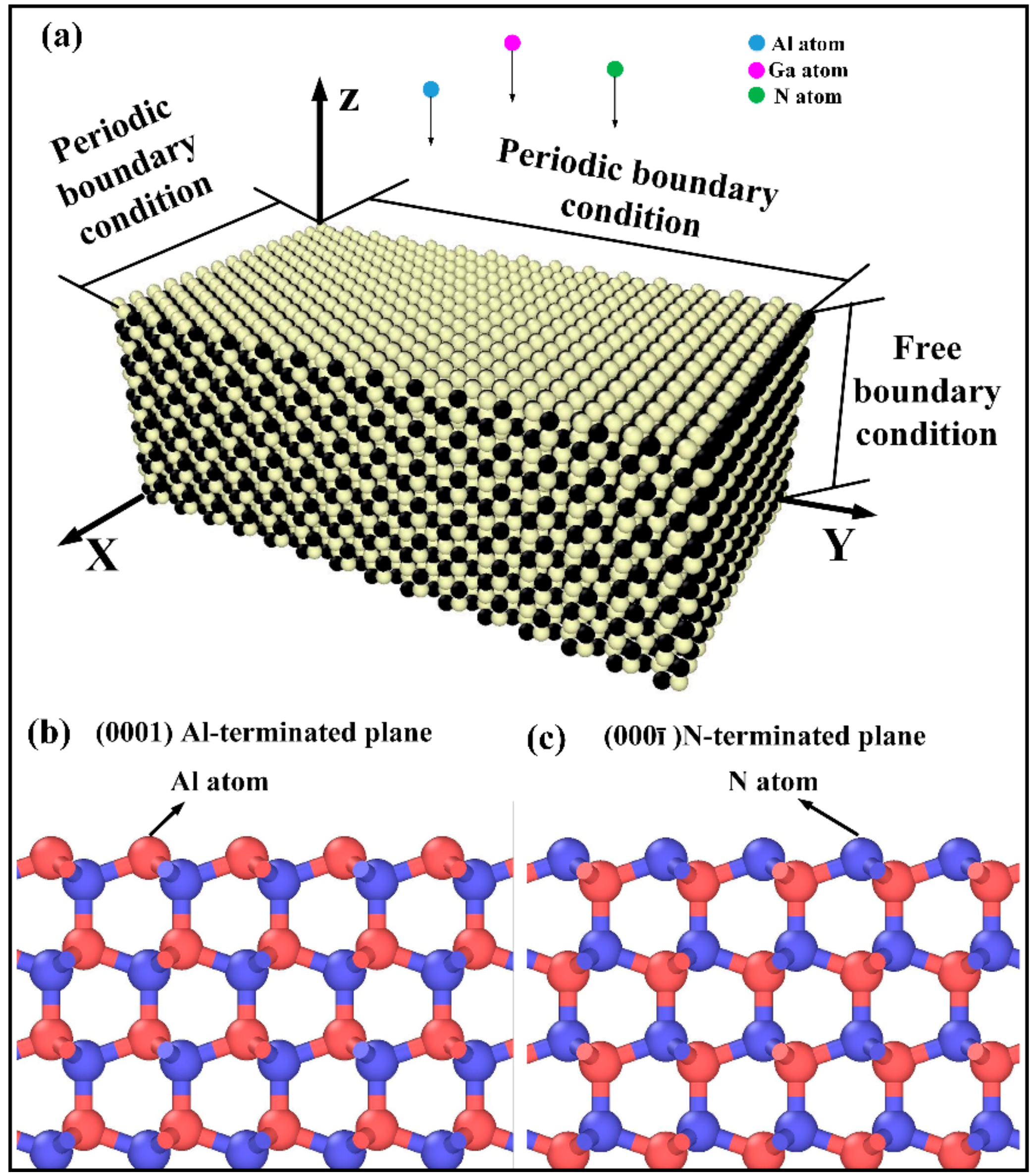
Figure 2.
AlGaN growth at 1350 K with injected Al:Ga ratio = 3:5 on (0001) Al-terminated AlN (a–d) and N-terminated AlN (e–h). The green, red and yellow indicate the Al, Ga and N atoms in the deposited film, respectively. In addition, the dark blue and light blue ball indicate the Al and N atoms in the substrate.
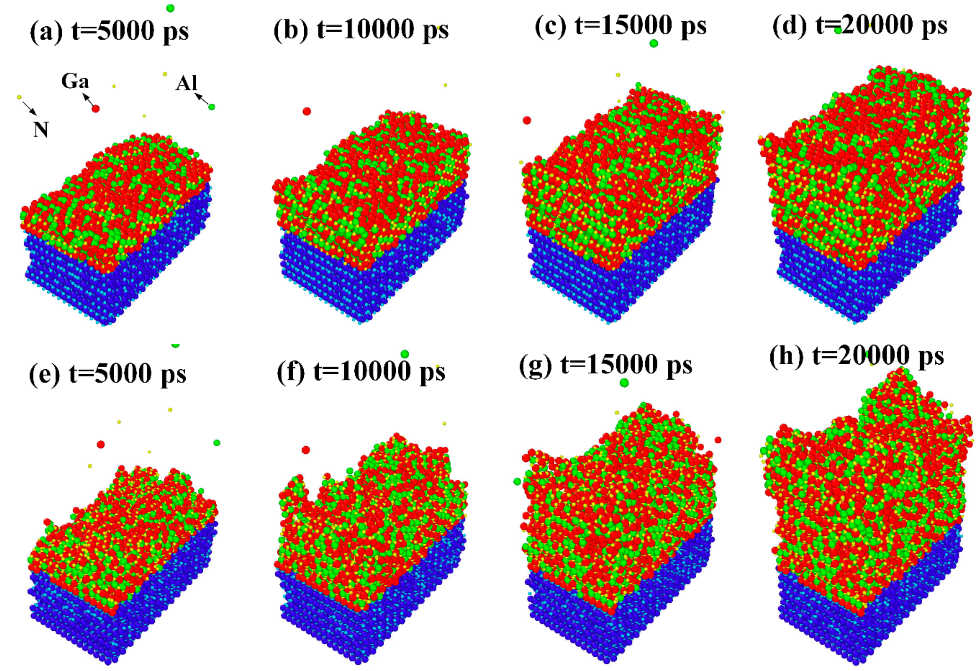
Figure 3.
Surface morphology of deposited AlGaN film with injected Al:Ga ratio of 3:5 at 950 K, 1150 K and 1350 K on: (a–c) (0001) Al-terminated AlN; (d–f) N-terminated AlN.
Figure 3.
Surface morphology of deposited AlGaN film with injected Al:Ga ratio of 3:5 at 950 K, 1150 K and 1350 K on: (a–c) (0001) Al-terminated AlN; (d–f) N-terminated AlN.

Figure 4.
Surface morphology of deposited AlGaN film at 1250 K with injected Al:Ga ratio of 3:5, 1:1 amd 5:3 on: (a–c) (0001) Al-terminated AlN; (d–f) N-terminated AlN.
Figure 4.
Surface morphology of deposited AlGaN film at 1250 K with injected Al:Ga ratio of 3:5, 1:1 amd 5:3 on: (a–c) (0001) Al-terminated AlN; (d–f) N-terminated AlN.

Figure 5.
Atomic scale structure of deposited AlGaN films at 950 K, 1150 K and 1350 K under different AlN substrates: (a–c) (0001) Al-terminated AlN; (d–f) N-terminated AlN. The red, green and yellow indicate the Al, Ga and N atoms in the deposited film, respectively. In addition, the dark blue and light blue balls indicate the Al and N atoms in the substrate.

Figure 6.
Atomic scale structure of deposited AlGaN films at 1350 K with injected Al:Ga ratio of 3:5, 1:1 and 5:3 under different AlN substrates: (a–c) (0001) Al-terminated AlN; (d–f) N-terminated AlN. The red, green and yellow indicate the Al, Ga and N atoms in the deposited film, respectively. In addition, the dark blue and light blue balls indicate the Al and N atoms in the substrate.

Figure 7.
Atomic structure and potential energy distribution of deposited AlGaN film with growth temperature of 1150 K and injected Al:Ga = 5:3. (a,b) shows the structural constituent of AlGaN films grown on (0001) Al-terminated and N-terminated AlN, while (c,d) shows the corresponding distribution of PE.

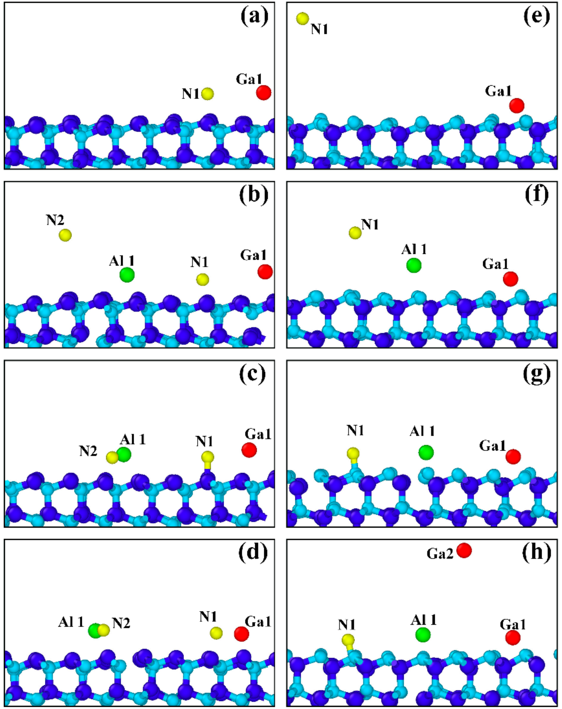
Figure 8.
Adatom migration process on different substrate surfaces: (a–d) on (0001) Al-terminated AlN surface and (e–h) on N-terminated AlN surface with growth temperature of 1450 K and injected Al:Ga = 1:1. The deep blue and light blue atoms represent Al and N atoms in the AlN substrate while the green, red, and yellow atoms represent Al, Ga and N atoms in the deposited film correspondingly.


Table 1.
SW potential parameters.
| Parameter | GaGa | NN | AlAl | GaN | GaAl | NAl |
|---|---|---|---|---|---|---|
| ε (eV) | 1.2000 | 1.2000 | 0.5650 | 2.1700 | 0.5223 | 2.2614 |
| σ (Å) | 2.1000 | 1.3000 | 2.6674 | 1.6950 | 2.7322 | 1.7103 |
| α | 1.60 | 1.80 | 1.55 | 1.80 | 1.55 | 1.80 |
| λ | 32.5 | 32.5 | 0.0 | 32.5 | 0.0 | 40.5 |
| γ | 1.2 | 1.2 | 1.2 | 1.2 | 1.2 | 1.2 |
| A | 7.9170 | 7.9170 | 17.8118 | 7.9170 | 17.8118 | 7.917 |
| B | 0.72 | 0.72 | 0.72 | 0.72 | 0.72 | 0.72 |
© 2018 by the authors. Licensee MDPI, Basel, Switzerland. This article is an open access article distributed under the terms and conditions of the Creative Commons Attribution (CC BY) license (http://creativecommons.org/licenses/by/4.0/).
Share and Cite
MDPI and ACS Style
Zhang, L.; Yan, H.; Zhu, G.; Liu, S.; Gan, Z.; Zhang, Z. Effect of Substrate Surface on Deposition of AlGaN: A Molecular Dynamics Simulation. Crystals 2018, 8, 279. https://doi.org/10.3390/cryst8070279
AMA Style
Zhang L, Yan H, Zhu G, Liu S, Gan Z, Zhang Z. Effect of Substrate Surface on Deposition of AlGaN: A Molecular Dynamics Simulation. Crystals. 2018; 8(7):279. https://doi.org/10.3390/cryst8070279
Chicago/Turabian StyleZhang, Libin, Han Yan, Guo Zhu, Sheng Liu, Zhiyin Gan, and Zili Zhang. 2018. "Effect of Substrate Surface on Deposition of AlGaN: A Molecular Dynamics Simulation" Crystals 8, no. 7: 279. https://doi.org/10.3390/cryst8070279
Note that from the first issue of 2016, this journal uses article numbers instead of page numbers. See further details here.