Multiscale Simulation of Surface Defects Influence Nanoindentation by a Quasi-Continuum Method

1
Department of Aeronautics and Astronautics, Fudan University, Shanghai 200433, China
2
Shanghai Institute of Measurement and Testing Technology, Shanghai 201203, China
*
Author to whom correspondence should be addressed.
Crystals 2018, 8(7), 291; https://doi.org/10.3390/cryst8070291
Submission received: 13 June 2018
/
Revised: 11 July 2018
/
Accepted: 12 July 2018
/
Published: 14 July 2018
(This article belongs to the Special Issue Selected Papers from "The 1st International Electronic Conference on Crystals")
Abstract
:Microscopic properties of nanocrystal aluminum thin film have been investigated using the quasicontinuum method in order to study the influence of surface defects in nanoindentation. Various distances between the surface defect and indenter have been taken into account. The results show that as the distance between the pit and indenter increases, the nanohardness increases in a wave pattern associated with a cycle of three atoms, which is closely related to the crystal structure of periodic atoms arrangement on {1 1 1} atomic close-packed planes of face-centered cubic metal; when the adjacent distance between the pit and indenter is more than 16 atomic spacing, there is almost no effect on nanohardness. In addition, the theoretical formula for the necessary load for elastic-to-plastic transition of Al film has been modified with the initial surface defect size, which may contribute to the investigation of material property with surface defects.
1. Introduction
Nanoindentation [1], which is relatively simple and effective, has already been used as a standard technique for evaluating mechanical properties of thin films [2,3,4,5,6,7]. Recently, a number of relevant scientists have focused on thin films with defects through simulations and experiment [8,9,10,11]. Yu and Shen observed the strong effects of the geometry of the nanocavity, which is one kind of defects in the film during the nanoindentation [12]. So far, surface roughness has become a major concern, which can be treated by the assembly of pits and steps, and many nanoindentation simulations near a step have been probed [13,14,15,16,17,18,19,20]. Furthermore, the surface pits defects can be seen in polycrystalline surfaces on microchips and micro-electro-mechanical systems (MEMS). Consequently, it is necessary and significant to observe on the nature of the pitted surface in nanoindentation. Ni Yushan et al. [21] studied nanoindentation of Al thin film and compared films with and without surface defects by multi-scale simulation, and Zhang et al. [22] has found the delay effect of dislocation nucleation with surface pit in nanoindentation. But the distance effect between the pit and indenter on elastic-plastic transition has not been taken into account, which is especially important to thin film performance in microchips and MEMS. Our aim is further to study the effect of distance of pit on nanohardness by quasicontinuum (QC) method [23], which is an relatively effective way to investigate large scale model, where the molecular dynamics (MD) is mostly limited by the model scale.
In the present article, fifteen distances of adjacent boundary between surface pit and indenter have been simulated by QC method to investigate the distance effect of pitted surface on nanohardness in nanoindentation. Compared with the nanoindentation on defect-free surface, the distance effect of pitted surface on elastic-plastic transition has been well explored and the theoretical formula of critical load for dislocation emission has been modified with initial surface pit.
2. Methodology
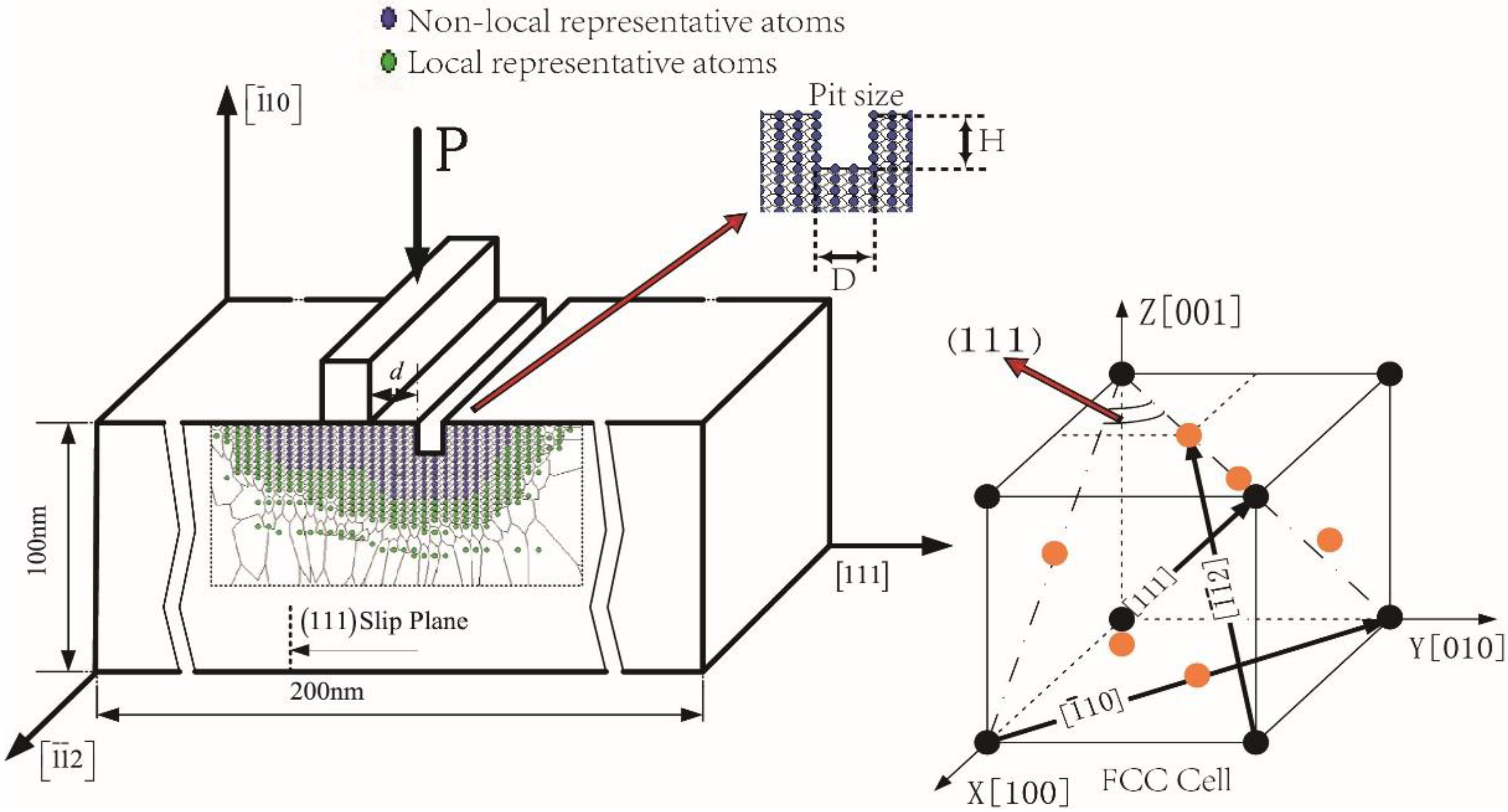
The Quasicontinuum (QC) method [24] is an effective mixed continuum and atomistic approach for simulating the mechanical response, especially in large-scale materials. The Ercolessi-Adams potential, which is one of the EAM potentials [25,26,27,28], is applied in this simulation to describe the atomistic behavior. The relevant material parameters of this potential in Al are showed as follows: the crystallographic lattice constant a1 is 0.4032 nm, one atomic lattice spacing in [1 1 1] direction (d0) is 0.2328 nm, one atomic spacing in direction (h0) is 0.1426 nm, Burgers vector is 0.285 nm, shear modulus μ is 33.14 GPa, Poisson ν is 0.319 and (1 1 1) surface energy γ111 is 0.869 J/m2, which is comparable with the experimental values of 1.14–1.20 J/m2 [29]. The elastic modulus predicted by this potential are C11 = 117.74 GPa, C12 = 62.06 GPa, and C44 = 36.67 GPa. The experimental values extrapolated to T = 0 K are C11 = 118.0 GPa, C12 = 62.4 GPa, and C44 = 32.5 GPa [25]. Figure 1 shows the nanoindentation model used in the simulation and the corresponding schematic of local and non-local representative atoms with initial surface pit, and its unit cell model of Al in the selected directions. The rectangular indenter is set rigid with its width of 0.932 nm (four times the lattice constant of Al in [1 1 1] direction (d0)). It is necessary to note that the indenter size is chosen refer to the ‘Nano-Indentation by a Square Punch’ simulation example in QC toturial document [30] and previous works [21,22]. The indenter shape is chosen rectangular in this simulation because the boundary of energy field (displacement field) and the distance between the pit and the indenter remain unchanged when driven down into the surface, which is exactly necessary to investigate the distance influence of the pit. The width D and depth H of surface pit are respectively 0.688 nm and 0.730 nm. We choose this pit size based on our previous works [21,22] and some necessary pre-simulations, which prove that such pit size is relatively moderate and proper, more sensitive to the distance effect. When the pit is too small, the influence of the pit on the nanohardness is not obvious; when the pit is too large, it is similar to that of a step, which is not exactly our focus. In the out-of-plane direction, the thickness of this model is equal to the minimal repeat distance with periodic boundary condition applied (namely 0.4938 nm for this model). The distance of adjacent boundary between the pit and indenter shows d in Figure 1. Fifteen different distances of adjacent boundary d have been simulated in this paper, which is respectively 1d0, 2d0, 3d0, 4d0, 5d0, 6d0, 7d0, 8d0, 9d0, 10d0, 11d0,12d0, 13d0, 17d0, 21d0. These distances are selected in order to make a more comprehensive investigation.
In QC method, the factor “PROXFACT” is used to determine the range of nonlocal effects. During a simulation, a repatom is made nonlocal if any pair of elements within PROXFACT*rcut of the repatom, where rcut is the atomistic potential cutoff radius, have significantly different deformation tensors. A “significant difference” is determined by comparing the difference between the eigenvalues of the elemental right Cauchy-Green deformation tensor C (C = FTF, where F is the deformation gradient) to the factor “epscr”, where the factor epscr is used to determine if a repatom must be made nonlocal due to significant variations in the deformation gradients around the repatom. Specifically, taking the eigenvalues of C in two elements a and b to be and (k = 1, 2, 3), nonlocality is triggered if .
The thin Al film in this simulation is 0.1 μm in height and 0.2 μm in width as shown in Figure 1, which is very large in normal atomistic modeling standards with almost 1.3 million atoms or about 4 million degrees of freedom. By contrast, multiscale simulation by QC method, which combines continuum mechanics and molecular mechanics, applies the MD model at the intense deformation region and a finite element model elsewhere for reducing the degrees of freedom and computational demand without losing atomistic required details. In this model, at most only 4000 atoms or 12,000 degrees of freedom are treated and such simulation can be run on personal computer in few days.
3. Results and Discussion
3.1. Nanohardness in the Case of no Surface Defect
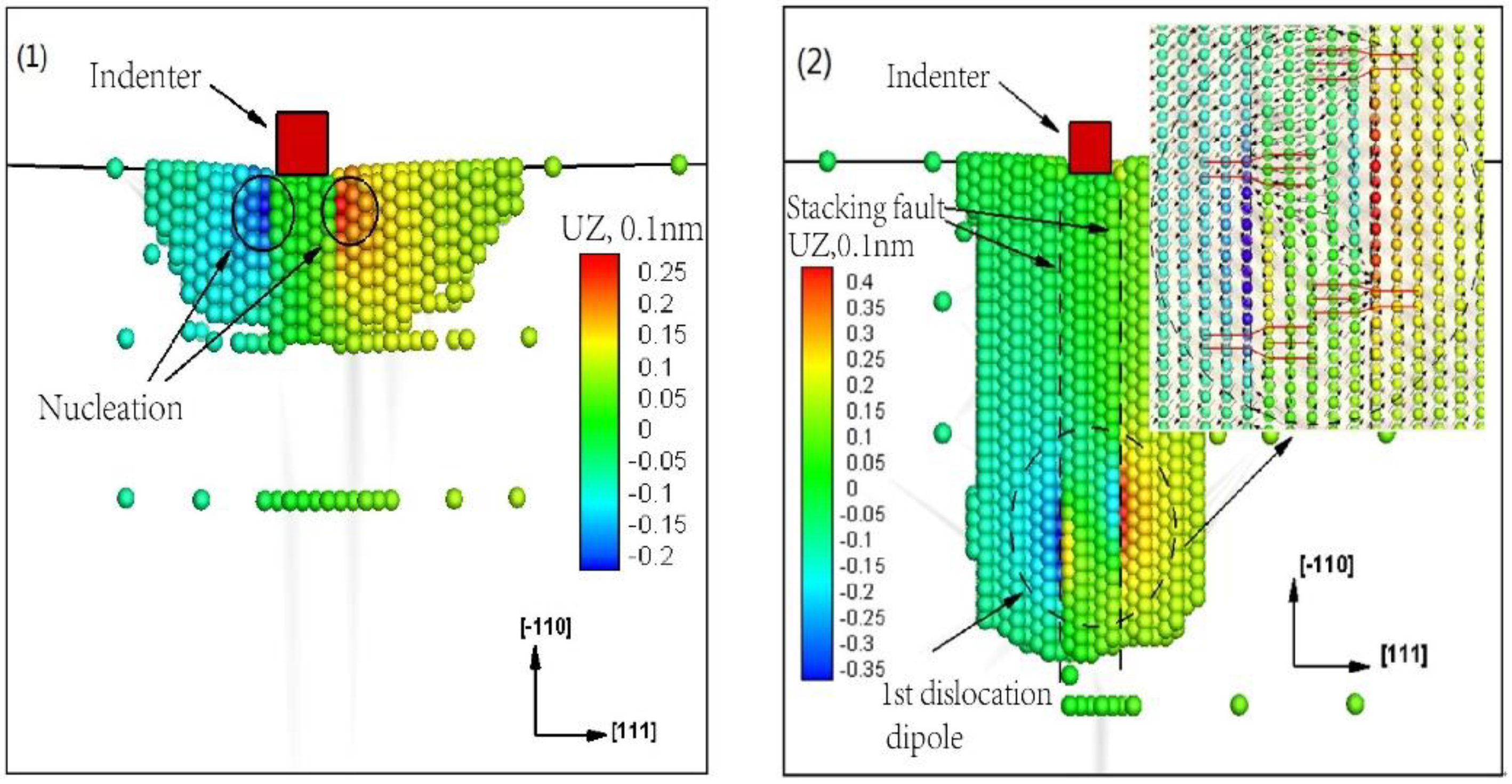
To make a comparison, a study of nanoindentation on a defect-free surface is carried out. The load-displacement curve shown the basic information obtained from nanoindentation simulations on defect-free surface is presented in Figure 2, where Load is expressed per unit length of indenter in the out-of-plane direction (N/m). It can be seen from Figure 2 that the load curve gradually increases during the initial loading process (OA), which indicates the elastic stage of thin films. The load increases to a maximum value of 15.14 N/m when the load step reaches 0.48 nm at point A. Then the load experiences an abrupt drop that it continually deceases to a minimum value of 7.67 N/m at point B.
To probe the potential mechanism of such abrupt decline of load (AB segment in Figure 2), the atomic positions and out-of-plane displacements are investigated. Figure 3 shows the atoms structure at the step of 0.48 nm and 0.50 nm, which are, respectively, corresponding point A and point B in Figure 2.
The conclusion can be drawn from Figure 3 that the load reaches the critical value for dislocation emission at point A, which indicates the beginning of plastic deformation stage. Then two Shockley partial dislocations are emitted at point B. The hardness is given by the equation [31]: , where is the maximum load and is the indentation area, the nanohardness of Al thin film is 16.24 GPa with no surface defect.
In this simulation, the indenter width is 0.932 nm, the yield load is about 15.14 N/m, and this is smaller than the value 24.7 N/m obtained by Tadmor and Miller [29] with defect-free surface, where the indentation size is 2.5 nm. It has been proved reasonably by a published observation [32] that a reduced width of indenter will make significant decrease in yield load result from the requirement decline of the necessary strain energy.
3.2. Nanohardness with Various Distances between Surface Defect and Indenter
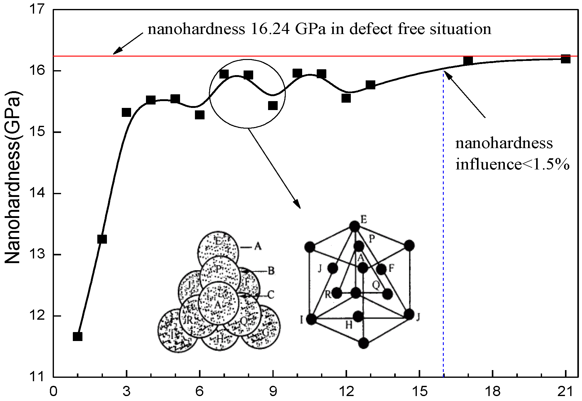
Figure 4 shows each nanohardness value in the case of nanoindentation on the thin film surface with and without surface pit. It indicates that the nanohardness of pitted surface is reduced, compared to one with no surface defect. This is reasonable because the surface pit defect creates a discontinuity at the boundary and the structure, which may lead to the decline of stain energy storage when indenting. Furthermore, when the distance of adjacent boundary between the pit and indenter d respectively equals 1d0, 2d0, 3d0, 4d0, 5d0, 6d0, 7d0, 8d0, 9d0, 10d0, 11d0, 12d0, 13d0, 17d0, 21d0, the nanohardness curve rises up in a wave pattern and finally tends towards the nanohardness value of no surface defect.
Through further investigation, it is found that this wave pattern is associated with a cycle of three atoms (donated by circle in Figure 4), which is closely related to the crystal structure. Moreover, different stacking patterns of atoms play a critical role in determining many physical properties, such as cleavage, electronic band structure, and optical transparency [33]. In this simulation, such periodic arrangement of atoms is “ABCABC” on {1 1 1} atomic close-packed planes of face-centered cubic metal (as shown in Figure 4 at the illustration). According to this simulation, when the simulation distance d increases each three atoms spacing on [1 1 1] direction, one cycle of atoms arrangement in “ABCABC” pattern is exactly finished. That is to say, when the pit moves away from the indenter every one atom in the [1 1 1] direction, the strain energy at the pit surface on the {1 1 1} stacking fault energies (SFE) changes, due to the proximity of the pit [34]. That’s why the nanohardness curve increases in a wave pattern associated with a cycle of three atoms.
In order to figure out the spatial extent of influence of surface pit on nanohardness, a further analysis is carried out. As Figure 4 shows, when the distance between the pit and indenter increases, the nanohardness approaches the nanohardness of no surface defect (16.24 GPa). If the influence of nanohardness is smaller than 1.5%, it can be considered that the surface pit almost does not affect the nanohardness. According to this simulation, when the distance (d) is more than 16 atomic spacing, there is almost no effect on nanohardness (as shown in Figure 4). It can be expected that different materials have such different critical values, which have significant meanings to the size design of thin layers in nanoindentation or microchips with the hardness guarantee.
However, the first three atoms, respectively d = 1d0, d = 2d0, d = 3d0 distance, do not match the wave pattern. To explain such special phenomenon, atomic structure and corresponding strain distribution of Al crystal are probed.
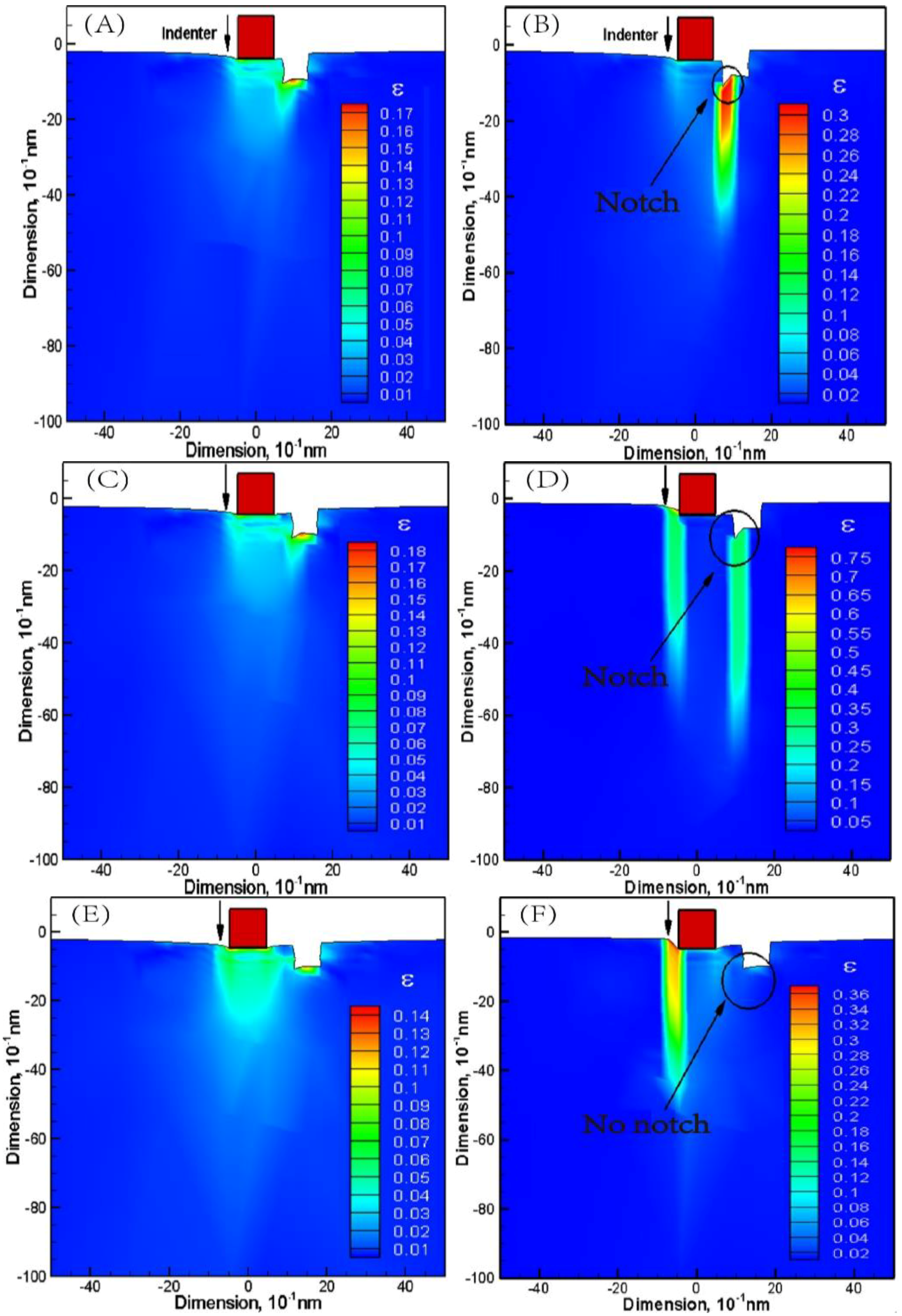
Figure 5 shows von Mises strain distribution of notch propagation and a comparison of strain before and after the notch when the distance d respectively equals 1d0, 2d0 and 3d0. It shows that when the distance d equals 1d0 and 2d0, there appears a notch phenomenon at the left side of surface pit, which directly induces serious damage to the structure of materials and great strain concentration (as shown in Figure 5A–D). When the distance d equals 3d0, there is no notch (as shown in Figure 5E,F). Consequently, when the distance d equals 1d0 and 2d0, the nanohardness is greatly reduced. That is to say that the first three atoms in nanohardness curve as shown in Figure 4 will not match the wave pattern associated with a cycle of three atoms.
3.3. Formula Modification of Necessary Load for Elastic-To-Plastic Transition
It is known that the influence of surface pit on nanohardness is actually the influence of dislocation nucleation and emission which is affected by surface pit. In order to further study the nanohardness calculation in the case of pitted surface, the calculation formula of necessary load for elastic-to-plastic transition is discussed and modified based on the model with no surface defect.
According to the critical load for dislocation emission, which is applied by Tadmor [29], the calculation formula of critical load for dislocation emission is displayed as following:
where Pcr is the critical load value at the onset of dislocation emission, k is the slope of elastic stage in the load-displacement curve, h is the depth of dislocation dipole when it is emitted, a is the half width of indenter, γ111 is the energy of (1 1 1) surface of Al crystal.
In order to make a more reasonable investigation, the data of simulation that d = 1d0 and d = 2d0 is not taken into account because of notch.
Table 1 shows the comparison of critical load between the QC method and dislocation theory, where “QC data” means the data of critical load in this simulation, and “theory load” means the data of critical load using Equation (1). It shows that in the case of every distance (d) simulation, the difference value between QC method and dislocation theory is changed frequently. According to the phenomenon discussed above that the nanohardness is periodically changed in a circle of three atoms, the critical load for dislocation emission is also in such periodicity. Consequently, the correction term (set as Δ) can be separated into two parts:
where A(d) is the correction part for the hardness decrease because of the surface pit and B·Sin(d) is just for the periodic change of atoms arrangement. It is well known that when the pit size (D, H as shown in Figure 1) is bigger, the value of critical load of dislocation emission is smaller [35]. So it is reasonable to apply (dividing by the crystallographic lattice constant can make it dimensionless, which has already been demonstrated reasonable in published article [36]) to express the size influence of surface pit. When the surface pit is infinitely far away from the indenter, the influence on nanohardness can be ignored, and if the pit size increases, the correction term changes more slowly with the distance variation. So, it is reasonable to apply to express the distance effect of surface pit. Furthermore, the effect of surface pit is closely related to the material property such as Burgers vector , shear modulus μ and Poisson ν. According to Equation (1), it is reasonable to apply to express the influence of material property. In addition, on {1 1 1} atomic close-packed planes of face-centered cubic metal, the periodic atoms arrangement is “ABCABC”. So the periodicity is three atoms. That is to say, it is reasonable to apply to express the periodicity of atoms arrangement. Considering that the unit of correction term (Δ) is N/m, and according to the discussion above, the correction term can be defined as following:
where , , are three constants that need to be optimized. According to the simulation data in Table 1, these three constants , and are approximately , , respectively. So the theoretical formula for necessary load of the first dislocation emission of Al film has been modified with initial surface pit as follows:
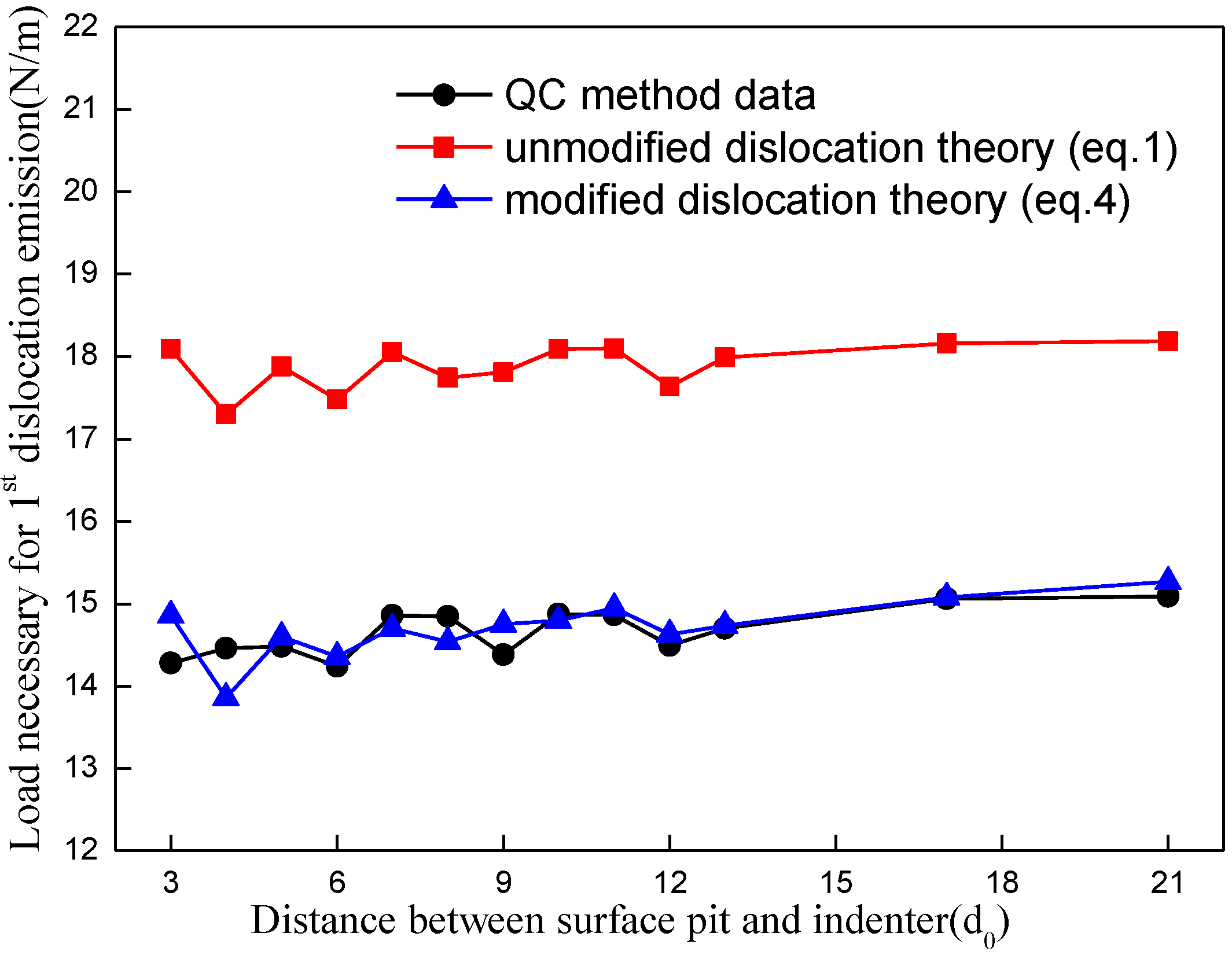
Figure 6 shows the comparison of the necessary load for elastic-to-plastic transition of Al thin film with various distances between the pit and the indenter calculated by the theoretical formula before and after modification. Though there is no parameter d in the unmodified dislocation theory (Equation (1)), the curves with blocks are calculated using depth h corresponding each distance case of surface pit and indenter in this simulation. It shows that the simulation QC data is closer to the theoretical results which are calculated by the Equation (4) after modification. That is to say, such modification to the theoretical formula is justified as the pit size and the distance between the pit and indenter have both been taken into account.
This modified formula describes the decreasing trend of nanohardness as the distance between the pit and indenter increases. This trend agrees with the experimental results of surface step with various distances [14]. Moreover, this modification may contribute to the investigation of the material property influenced by the surface defects, particularly in mircochips and MEMS.
4. Conclusions
In this paper, the QC method is employed to investigate the distance effect of the pitted surface on elastic-plastic transition. Compared with the nanoindentation on defect-free surfaces, fifteen various distances of adjacent boundaries between the pit and indenter are taken into account. The conclusion can be drawn as follows:
- The pitted surface plays a great role in the emission of dislocation that it causes significant reduction on nanohardness, compared with defect-free situation.
- As the distance between the pit and indenter increases, nanohardness increases in a wave pattern associated with a cycle of three atoms, which is closely related to periodic atoms arrangement on {1 1 1} atomic close-packed planes of face-centered cubic metal; when the adjacent distance between the pit and indenter is more than 16 atomic spacing, there is almost no effect on nanohardness.
- The theoretical formula for necessary load of the elastic–plastic transition of Al film has been effectively modified to accommodate the effect of the initial surface pit. This modified formula closely fits the decreasing trend of nanohardness as the distance between the pit and indenter increases, and such trend agrees well with the experimental results of surface step with various distances. Such modification may contribute to the investigation of material property with surface defects, particularly in mircochips and MEMS.
Author Contributions
Conceptualization, Y.N.; Data curation, Z.Z., J.Z., C.W., K.J. and X.R.; Formal analysis, Z.Z.; Funding acquisition, Y.N.; Investigation, Z.Z.; Methodology, Y.N.; Project administration, Y.N.; Supervision, Y.N.; Validation, Z.Z., J.Z., C.W., K.J. and X.R.; Visualization, Z.Z., J.Z., C.W., K.J. and X.R.; Writing—original draft, Y.N. and C.W.; Writing—review and editing, Z.Z.
Funding
This work is supported by the National Natural Science Foundation of China (Grant No. 11572090).
Acknowledgments
The authors would like to thank Professor Tadmor E. B. and Miller R. for their quasicontinuum code and suggestions during the multiscale simulations.
Conflicts of Interest
The authors declare no conflict of interest. The founding sponsors had no role in the design of the study; in the collection, analyses, or interpretation of data; in the writing of the manuscript, and in the decision to publish the results.
References
- Oliver, W.C.; Pharr, G.M. An improved technique for determining hardness and elastic modulus using load and displacement sensing indentation experiments. J. Mater. Res. 1992, 7, 1564–1583. [Google Scholar] [CrossRef]
- Li, X.D.; Bhushan, B. A review of nanoindentation continuous stiffness measurement technique and its applications. Mater. Charact. 2002, 48, 11–36. [Google Scholar] [CrossRef]
- Bamber, M.J.; Cooke, K.E.; Mann, A.B.; Derby, B. Accurate determination of Young’s modulus and Poisson’s ratio of thin films by a combination of acoustic microscopy and nanoindentation. Thin Solid Films 2001, 399, 299–305. [Google Scholar] [CrossRef]
- Zhu, P.Z.; Hu, Y.Z.; Fang, F.Z.; Wang, H. Multiscale simulations of nanoindentation and nanoscratch of single crystal copper. Appl. Surf. Sci. 2012, 258, 4624–4631. [Google Scholar] [CrossRef]
- Chen, J.; Bull, S.J. Assessment of the toughness of thin coatings using nanoindentation under displacement control. Thin Solid Films 2006, 494, 1–7. [Google Scholar] [CrossRef]
- Sangwal, K.; Gorostiza, P.; Sanz, F. Atomic force microscopy study of nanoindentation creep on the (100) face of MgO single crystals. Surf. Sci. 2000, 446, 314–322. [Google Scholar] [CrossRef]
- Zhang, T.H.; Yang, Y.M. The application of nanohardness technology in the mechanical properties testing of surface engineering. Chin. Mech. Eng. 2002, 24, 85–88. [Google Scholar]
- Mitchell, T.E. Dislocations and plasticity in single crystals of face centered cubic metals and alloys. Prog. Appl. Mater. Res. 1964, 6, 117–238. [Google Scholar]
- Mitchell, J.W. Growth and Perfection of Crystals; Doremus, R.H., Roberts, B.W., Turnbull, D., Eds.; Wiley: New York, NY, USA, 1958; pp. 386–389. [Google Scholar]
- Yang, B.; Vehoff, H. Dependence of nanohardness upon indentation size and grain size—A local examination of the interaction between dislocations and grain boundaries. Acta Mater. 2007, 55, 849–856. [Google Scholar] [CrossRef]
- Soifer, Y.M.; Verdyan, A.; Kazakevich, M.; Rabkin, E. Nanohardness of copper in the vicinity of grain boundaries. Scr. Mater. 2002, 47, 799–804. [Google Scholar] [CrossRef]
- Yu, W.S.; Shen, S.P. Multiscale analysis of the effects of nanocavity on nanoindentation. Comp. Mat. Sci. 2009, 46, 425–430. [Google Scholar] [CrossRef]
- Shan, D.; Yuan, L.; Guo, B. Multiscale simulation of surface step effects on nanoindentation. Mat. Sci. Eng. A 2005, 412, 264–270. [Google Scholar] [CrossRef]
- Keily, J.D.; Hwang, R.Q.; Houston, J.E. Effect of surface steps on the plastic threshold in nanoindentation. Phys. Rev. Lett. 1998, 81, 4424–4427. [Google Scholar] [CrossRef]
- Gouldstone, A.; Van Vliet, K.J.; Suresh, S. Nanoindentation: Simulation of defect nucleation in a crystal. Nature 2001, 411, 656–657. [Google Scholar] [CrossRef] [PubMed]
- Zimmerman, J.A.; Kelchner, C.L.; Klein, P.A.; Hamilton, J.C.; Foiles, S.M. Surface step effects on nanoindentation. Phys. Rev. Lett. 2001, 87, 165507–165561. [Google Scholar] [CrossRef] [PubMed]
- Jiang, W.G.; Su, J.J.; Feng, X.Q. Effect of surface roughness on nanoindentation test of thin films. Eng. Fract. Mech. 2008, 75, 4965–4972. [Google Scholar] [CrossRef]
- Miller, R.E.; Shilkrot, L.E.; Curtin, W.A. A coupled atomistics and discrete dislocation plasticity simulation of nanoindentation into single crystal thin films. Acta Mater. 2004, 52, 271–284. [Google Scholar] [CrossRef]
- Tsuru, T.; Shibutani, Y. Anisotropic effects in elastic and incipient plastic deformation under (001), (110), and (111) nanoindentation of Al and Cu. Phys. Rev. B. 2007, 75, 035415–035421. [Google Scholar] [CrossRef]
- Wagner, R.J.; Ma, L.; Tavazza, F.; Levine, L.E. Dislocation nucleation during nanoindentation of aluminum. J. Appl. Phys. 2008, 104, 114311–114312. [Google Scholar] [CrossRef]
- Li, J.W.; Ni, Y.S.; Lin, Y.H.; Luo, C. Multiscale simulation of nanoindentation on Al thin film. Acta Metall. Sin. 2009, 45, 129–136. [Google Scholar]
- Zhang, Z.L.; Ni, Y.S. Multiscale analysis of delay effect of dislocation nucleation with surface pit defect in nanoindentation. Comp. Mat. Sci. 2012, 62, 203–209. [Google Scholar] [CrossRef]
- Qin, Z.D.; Wang, H.T.; Ni, Y.S. Multiscale simulations of FCC Al nanoindentation. Chin. Q. Mech. 2007, 1, 46–53. [Google Scholar]
- Tadmor, E.B. The Quasicontinuum Method. Ph.D. Thesis, Brown University, Providence, RI, USA, 1996. [Google Scholar]
- Ercolessi, F.; Adams, J.B. Interatomic potentials from first-principles calculations: The force-matching method. Europhys. Lett. 1994, 26, 583–588. [Google Scholar] [CrossRef]
- Tadmor, E.B.; Ortiz, M.; Phillips, R. Quasicontinuum analysis of defects in solids. Philos. Mag. A 1996, 73, 1529–1563. [Google Scholar] [CrossRef]
- Tadmor, E.B.; Phillips, R.; Ortiz, M. Mixed atomistic and continuum models of deformation in solids. Langmuir 1996, 12, 4529–4534. [Google Scholar] [CrossRef]
- Shenoy, V.B.; Miller, R.; Tadmor, E.B.; Rodney, D.; Phillips, R.; Ortiz, M. An adaptive finite element approach to atomic-scale mechanics—The quasicontinuum method. J. Mech. Phys. Solids 1999, 47, 611–642. [Google Scholar] [CrossRef]
- Tadmor, E.B.; Miller, R.; Phillips, R. Nanoindentation and incipient plasticity. J. Mater. Res. 1999, 14, 2233–2250. [Google Scholar] [CrossRef] [Green Version]
- QC Tutorial Guide Version 1.4. Available online: http://qcmethod.org/documentation (accessed on 26 June 2018).
- Nanoindentation. Available online: https://en.wikipedia.org/wiki/Nanoindentation (accessed on 2 May 2018).
- Jiang, W.G.; Li, J.W.; Su, J.J.; Tang, J.L. Quasicontinuum analysisi of indenter size effect in nanoindentation tests. Chin. J. Solid Mech. 2007, 4, 375–379. [Google Scholar]
- Crystal Strucrure. Available online: https://en.wikipedia.org/wiki/Crystal_structure (accessed on 20 June 2018).
- Lu, G.; Kioussis, N.; Bulatov, V.V.; Kaxiras, E. Generalized-stacking-fault energy surface and dislocation properties of aluminum. Phys. Rev. B 2000, 62, 3099–3108. [Google Scholar] [CrossRef] [Green Version]
- Abu Al-Rub, R.K.; Voyiadjis, G.Z. A physically based gradient plasticity theory. Int. J. Plast. 2006, 22, 654–684. [Google Scholar] [CrossRef]
- Zhang, Z.L.; Ni, Y.S.; Zhang, J.M.; Wang, C.; Ren, X.D. Multiscale analysis of size effect of surface pit defect in nanoindentation. Micromachines 2018, 9, 298. [Google Scholar] [CrossRef]
Figure 1.
The schematic illustration of nanoindentation model with a pit defect and its unit cell model of Al in the selected directions, where the unusual shapes in local region are not finite elements, they are just the schematic of its specific region that one corresponding representative atom belongs to.

Figure 2.
Load-displacement curves for nanoindentation on Al film without surface pit.

Figure 3.
Snapshot of atoms under indenter and corresponding out-of-plane displacement plot, where UZ is atom displacement at out-of-plane. (1) point A in Figure 2 (dislocation nucleation); (2) point B in Figure 2 (dislocation emission).

Figure 4.
Nanohardness vs. distance of adjacent boundary between the pit and indenter.

Figure 5.
Von Mises strain distribution of notch propagation. (A) d = 1d0 at the load step of the indenter 0.38 nm; (B) d = 1d0 at the load step of the indenter 0.4 nm; (C) d = 2d0 at the load step of the indenter 0.44 nm; (D) d = 2d0 at the load step of the indenter 0.46 nm; (E) d = 3d0 at the load step of the indenter 0.46 nm; (F) d = 3d0 at the load step of the indenter 0.48 nm.

Figure 6.
The comparison of the necessary load for elastic-to-plastic transition of Al thin film with various distances between the pit and the indenter calculated by the theoretical formula before and after modification.
Figure 6.
The comparison of the necessary load for elastic-to-plastic transition of Al thin film with various distances between the pit and the indenter calculated by the theoretical formula before and after modification.


Table 1.
The comparison of critical load between QC method and dislocation theory.
| Distance (d0) | QC Data (N/m) | Theory Load (N/m) | Data Difference (N/m) |
|---|---|---|---|
| 3 | 14.28 | 18.02 | 3.75 |
| 4 | 14.46 | 17.29 | 2.83 |
| 5 | 14.48 | 17.88 | 3.39 |
| 6 | 14.24 | 17.41 | 3.15 |
| 7 | 14.86 | 17.96 | 3.14 |
| 8 | 14.85 | 17.65 | 2.83 |
| 9 | 14.38 | 17.92 | 3.07 |
| 10 | 14.87 | 17.87 | 3.49 |
| 11 | 14.86 | 18.03 | 3.16 |
| 12 | 14.49 | 17.56 | 2.70 |
| 13 | 14.70 | 17.99 | 3.50 |
| 17 | 15.06 | 18.04 | 3.34 |
| 21 | 15.09 | 18.17 | 3.11 |
© 2018 by the authors. Licensee MDPI, Basel, Switzerland. This article is an open access article distributed under the terms and conditions of the Creative Commons Attribution (CC BY) license (http://creativecommons.org/licenses/by/4.0/).
Share and Cite
MDPI and ACS Style
Zhang, Z.; Ni, Y.; Zhang, J.; Wang, C.; Jiang, K.; Ren, X. Multiscale Simulation of Surface Defects Influence Nanoindentation by a Quasi-Continuum Method. Crystals 2018, 8, 291. https://doi.org/10.3390/cryst8070291
AMA Style
Zhang Z, Ni Y, Zhang J, Wang C, Jiang K, Ren X. Multiscale Simulation of Surface Defects Influence Nanoindentation by a Quasi-Continuum Method. Crystals. 2018; 8(7):291. https://doi.org/10.3390/cryst8070291
Chicago/Turabian StyleZhang, Zhongli, Yushan Ni, Jinming Zhang, Can Wang, Kun Jiang, and Xuedi Ren. 2018. "Multiscale Simulation of Surface Defects Influence Nanoindentation by a Quasi-Continuum Method" Crystals 8, no. 7: 291. https://doi.org/10.3390/cryst8070291
Note that from the first issue of 2016, this journal uses article numbers instead of page numbers. See further details here.