Deposition Technologies of High-Efficiency CIGS Solar Cells: Development of Two-Step and Co-Evaporation Processes


Department of Electrical Engineering, National Dong Hwa University, No. 1, Sec. 2, University Road, ShouFeng, Hualien 97401, Taiwan
*
Author to whom correspondence should be addressed.
Crystals 2018, 8(7), 296; https://doi.org/10.3390/cryst8070296
Submission received: 31 May 2018
/
Revised: 15 July 2018
/
Accepted: 16 July 2018
/
Published: 18 July 2018
(This article belongs to the Special Issue Selected Papers from Taiwan Association for Academic Innovation, TAAI 2018)
Abstract
:The two-step process including the deposition of the metal precursors followed by heating the metal precursors in a vacuum environment of Se overpressure was employed for the preparation of Cu(In,Ga)Se2 (CIGS) films. The CIGS films selenized at the relatively high Se flow rate of 25 Å/s exhibited improved surface morphologies. The correlations among the two-step process parameters, film properties, and cell performance were studied. With the given selenization conditions, the efficiency of 12.5% for the fabricated CIGS solar cells was achieved. The features of co-evaporation processes including the single-stage, bi-layer, and three-stage process were discussed. The characteristics of the co-evaporated CIGS solar cells were presented. Not only the surface morphologies but also the grading bandgap structures were crucial to the improvement of the open-circuit voltage of the CIGS solar cells. Efficiencies of over 17% for the co-evaporated CIGS solar cells have been achieved. Furthermore, the critical factors and the mechanisms governing the performance of the CIGS solar cells were addressed.

1. Introduction
The CIGS-based films are commonly prepared by the two-step or co-evaporation processes, where the two-step process is also called the sulfurization after selenization (SAS) process [1]. The thin-film CIGS solar cells have reached efficiencies of over 20%, where the CIGS films were prepared by the co-evaporation method [2,3,4,5]. Recently, efficiency of 22.9% for the laboratory-scale CIGS-based solar cells prepared by the two-step process was reported [6]. The efficiency of the champion CIGS solar cell has surpassed that of the polycrystalline Si solar cells [6]. Besides the vacuum processes, the non-vacuum processes including the printing [7], electrodeposition [8], and solution-processed [9] techniques have been applied to deposit device-quality CIGS films. The efficiencies of the CIGS solar cells prepared by these non-vacuum processes have exceeded 15% [8,9]. The printing method has even achieved efficiency of 17.1% [7]. In addition, a low-temperature pulsed electron deposition method for the growth of CIGS films was reported, by which a conversion efficiency of 17.0% for the CIGS solar cell was obtained [10]. Among various deposition methods, the two-step and co-evaporation processes have been widely employed for mass production of the large-scale CIGS-based modules [11,12]. Another favorite approach in CIGS industry is the rapid thermal process (RTP), in which a thin Se layer is first capped on the top of metal precursors, CuInGa compounds, and then the diluted H2S gas is supplied to simultaneously sulfurize and selenize the precursors to form the Cu(In,Ga)(S,Se)2 (CIGSS) films in an RTP furnace [13].
The two-step process for the preparation of the CIGS films can be easily scaled up for mass production. In order to achieve high-performance, the two-step process typically employs H2Se gas to selenize the metal precursors. However, H2Se gas is fatally toxic and flammable. The processing of H2Se must be handled with extreme caution. Alternatively, the two-step process can be conducted by using less toxic Se vapor. In order to take advantage of the less toxic elemental Se source and understand the factors impacting the performance of CIGS solar cells prepared with Se vapor, the dependence of the process conditions on the resulting characteristics of the CIGS films were explored in this research. Moreover, the CIGS solar cells prepared by the two-step process were fabricated and characterized.
The co-evaporation process is a superior approach for the fabrication of CIGS-based solar cells with respect to device performance, although high efficiencies can also be achieved with the two-step process. Furthermore, the co-evaporation method provides the most flexible capabilities to develop the different deposition procedures for the growth of the CIGS films, such as the bi-layer process [14,15] and three-stage process [16]. Not only can the precise control of the compositions for the as-deposited CIGS films be easily achieved, but also the grading bandgap structures, resulting from various depth profiles of Ga distribution within the CIGS films, can be realized by using the co-evaporation process. In this study, the characteristics of CIGS films deposited by different co-evaporation processes including the single-stage, bi-layer, and three-stage processes were analyzed, and their impacts on the performance of CIGS solar cells were discussed. The correlations of the deposition process, film properties, and cell performance were investigated.
2. Experimental Details
2.1. CIGS Film Preparation and Device Fabrication
The CIGS films were prepared by the two-step process which consisted of the preparation of the metal precursors followed by heating the metal precursors in an environment containing an overpressure of Se vapor. The metal precursors of a stack of CuGa and In layers were sequentially sputtered on the Mo coated glass substrates for the first step. The metal precursors were then selenized by evaporating the solid Se source to maintain the overpressure of Se vapor in vacuum. A thermal evaporation system equipped with a Knudsen-type effusion cell for the evaporation of Se source was employed to selenize the metal precursors. During the selenization, the process was conducted by heating the metal precursors with two sequential stages including an initial low-temperature stage and a subsequent high-temperature stage.
The thermal evaporation system, the same system used for the two-step process, consists of four Knudsen-type effusion cells of Cu, In, Ga, and Se and is also employed for the co-evaporation of the CIGS films. To control the overall compositions and the element distributions of the as-deposited films, the metal fluxes of Cu, In, and Ga were monitored by electron impact emission spectroscopy (EIES, Sigma Instruments, Butler County PA, USA), and the Se flux rate was detected by quartz crystal microbalance (QCM, Sigma Instruments, USA)during the deposition. After the deposition was completed, the samples were cooled down under an overpressure of Se vapor maintained in the chamber until the substrate temperature dropping down to 200 °C. The deposition time was adjusted to acquire the film thicknesses of approximately 2~2.5 μm.
The CIGS solar cells with a device structure of glass/Mo/CIGS/CdS/i-ZnO/Al doped ZnO/MgF2 were fabricated. The back contacts of Mo, CIGS, buffer CdS, intrinsic ZnO (i-ZnO), Al doped ZnO (ZnO:Al) layers were sequentially deposited by sputtering, two-step or co-evaporation, chemical bath deposition (CBD), and sputtering processes, respectively. The size of total area for each cell was 0.43 cm2. A bilayer of Ni and Al films was employed as the metal grids of the cells, which covered 5% of the total cell area. The anti-reflection layers of MgF2 were finally deposited by the e-beam process.
2.2. Film and Device Characterization
The crystal structures and composition of the as-deposited films were characterized by X-ray diffraction (XRD) and inductively coupled plasma optical emission spectrometer (ICP-OES, model number: Optima 7000 DV, PerkinElmer, Waltham, MA, USA), respectively. The morphologies and cross-sectional views of the deposited films were studied by scanning electron microscopy (SEM, JSM-7000F JEOL Ltd., Tokyo, Japan). The depth profiles of element distribution within the CIGS films were measured by secondary ion mass spectrometry (SIMS, IMS-6f, CAMECA, Pairs, France). The photo-current–voltage (I-V) measurements of CIGS solar cells were performed under the Standard Reporting Conditions (SRC) specifying the total radiation level of 100 mW/cm2, device temperature of 25 °C, and reference spectral radiance distribution of AM1.5G.
3. Results and Discussion
3.1. Two-Step Process
The heating profile of the two-step process to selenize the metal precursors is illustrated in Figure 1a. The heating temperatures of the first selenization stage were in the range of 200 °C to 350 °C for 10–50 min, and those of the second selenization stage were in the range of 400 °C to 580 °C for 10–80 min. After the selenization stages were completed, without using the cooling system, the samples were directly cooled down under the Se vapor until the substrate temperatures dropped to 200 °C. The current density-voltage (J-V) results of a CIGS solar cell prepared by the two-step process are given in Figure 1b.
The J-V characteristic behavior of the CIGS solar cells is depicted by an equation of the single-diode model as follows [17].
The precursors with the low or high Ga contents were prepared and they were then selenized at the low selenium flow rate of 15 Å/s or the high selenium flow rate of 25 Å/s. The corresponding atomic ratios of the bulk compositions for the selenized CIGS films are listed in Table 1. For the preparation of CIGS films, the thicknesses of CuGa and In layers of the metal precursors were tuned in order to obtain slightly Cu-poor CIGS films in terms of the device-quality films. For the results shown in Table 1, the atomic ratios of Cu for the as-prepared CIGS films ranged from 21.4% to 22.8%, resulting in the Cu/(Ga + In) (CGI) ratios varying from 0.77 to 0.84. Additionally, it is clear that the high selenium atomic ratios of around 51% or more could be achieved by employing the higher selenium flow rate of 25 Å/s for either the low or high Ga-content metal precursors. After selenization, the low and high Ga-content metal precursors were turned into the CIGS films with Ga/(Ga + In) (GGI) ratios of 0.18 and 0.25, respectively, as shown in Table 1. The bandgap energies of the CIGS films with the GGI ratios of 0.18 and 0.25 were estimated around 1.11 eV and 1.14 eV, respectively [19]. Although typically the bandgap energies of around 1.4–1.5 eV, which could be achieved by further increasing the Ga contents for the CIGS films, are ideal for the photovoltaic devices under the solar spectrum of AM1.5G, the high Ga contents lead to the formation of the deep-level defects, degrading the performance of the CIGS solar cells [20]. From the aspects of compositions for the device-grade CIGS films, the CGI and GGI ratios of the as-prepared CIGS films were within the preferable ranges.
The composition data is shown in Table 1, the performance parameters of the CIGS solar cells fabricated from the selenized CIGS films are displayed in Table 1 as well. The current density-voltage characteristics of the best CIGS solar cell fabricated with the given selenization conditions is presented in Figure 1b, where the process conditions were 15 min at 300 °C for the first stage and 35 min at 570 °C for the second stage. The total-area efficiency of 11.8% was achieved, and the active-area efficiency of this CIGS solar cell was 12.5%.
Under the condition of illumination, the value of the diode ideality factor for the CIGS solar cells is 1.85, suggesting that the space-charge region (SCR) recombination was still dominant in the cell. The value of the parasitic resistance, namely the series resistance, is greater in the dark condition than that under illumination. Since there is a dependence of the series resistance on the derivative of dJ/dV, which is the slope of the J-V curve, in the first quadrant. A greater slope of the J-V curve in the first quadrant leads to smaller series resistance and vice versa. Due to the different slopes of the J-V curves in the first quadrant for the dark and light conditions, a crossover between light and dark J-V curves occurred in the first quadrant, which is often observed in the CIGS solar cells. This effect, resulting from the conduction barrier produced between the CIGS and CdS layers, has been reported [21,22].
As the SEM images show in Figure 2, for the metal precursors of either the low or high Ga contents, the number of voids was significantly decreased for the CIGS films selenized at the high selenium flow rate. The compact, dense, and well-faceted grains were obtained for the CIGS films selenized at the high selenium flow rate, which is beneficial to the surface morphology of the CIGS films. The deposition of the CIGS films was followed by the growth of the CdS buffers. Since the CIGS films prepared at the high Se flow rate had improved surface morphologies, as illustrated in Figure 2, a better coverage of buffers on the smoother CIGS films could be formed, leading to the diminishment of the shunt path for the fabricated solar cells. Thus, both open-circuit voltage (VOC) and fill factor (FF) of the low and high Ga content CIGS solar cells prepared at the high Se flow rate of 25 Å/s were enhanced, as shown in Table 1. Attributed to the fewer voids and the improved surface morphology of the CIGS films prepared at the high Se flow rate of 25 Å/s, the conformal coverage of the chemical-bath-deposited buffer layers formed on the CIGS surface led to the preferable interface properties between the buffers and CIGS films as well as the improved junction properties for the CIGS solar cells. As illustrated in Figure 3a, the CdS buffer provided good coverage on the CIGS film selenized at the Se rates of 25 Å/s. The shunt path from the CIGS films to the top contacts was thus effectively restrained. With fewer voids on the surface of the CIGS films selenized at the Se rates of 25 Å/s as the samples (c) and (d) shown in Figure 2, the carrier recombination around the junction region of the CIGS solar cells was suppressed. Hence, for the samples (c) and (d) shown in Table 1, the open-circuit voltage was further improved. Besides considering the coverage of the buffers, the thicknesses of buffers were optimized to maintain the high transmission by controlling the deposition time during the CBD process as well. The cross-sectional view of the complete structure of CIGS solar cells is shown in Figure 3b.
As shown in Table 1, the dependence of the open-circuit voltage on the Ga contents of the CIGS films was evident. For the films selenized at the same Se flow rates of 15 Å/s or 25 Å/s, the cells (b) and (d) had the larger open-circuit voltages, resulting from the wider bandgap of the CIGS films with a higher GGI ratio of 0.25. However, the short-circuit current densities (JSC) were just slightly decreased with the increase of the Ga contents in the CIGS films. The reasons were twofold. The bandgap energies near the surface region of the low and high Ga content CIGS films were nearly the same because Ga was piled up around the back region of the CIGS films, as shown in Figure 4. Moreover, most of the incident photons were absorbed near the surface region of CIGS solar cells. Therefore, for the CIGS films prepared at the same Se flow rates, the short-circuit current densities of the high Ga content CIGS solar cells prepared did not drop dramatically.
For the fabricated CIGS solar cells with the GGI ratios around 18% and 25%, corresponding to the estimated bandgap energies of 1.11 eV and 1.14 eV, respectively, the achieved short-circuit current densities were exceedingly high, and the open-circuit voltages were much smaller than expected. The main mechanism responsible for the high JSC as well as the low VOC could be attributed to the accumulated Ga content near the Mo contacts. Figure 4 shows the SIMS depth profile of composition distribution for the CIGS film with a Ga/(Ga + In) ratio of 0.25 selenized at the Se flow rate of 25 Å/s. Similar results of Ga accumulation near the Mo/CIGS interface for the two-step process were reported [23,24,25,26]. Due to the accumulation of Ga around the bottom of CIGS films, as shown in Figure 4, the bandgap energy around the surface region of CIGS films is close to 1.02 eV, resulting from the very low Ga content near the space charge region of the cells. This low bandgap energy of about 1.02 eV around the space charge region led to the low open-circuit voltages and high short-circuit current densities of the fabricated CIGS solar cells prepared by the given selenization conditions.
3.2. Effects of Ga Content on the Co-Evaporated CIGS Solar Cells
The composition of CIGS films plays a key role in governing the semiconductor properties of the as-deposited films. The impacts of composition on the characteristics of CIGS solar cells prepared by single-stage and three-stage processes were investigated and discussed as follows. The dependence of the performance parameters on the CGI and GGI ratios of the CIGS films prepared by the single-stage process is presented in Figure 5. In accordance with the pseudobinary In2Se3-Cu2Se equilibrium phase diagram [27], the atomic percentages of Cu contents in the device-quality CuInSe2 films, namely the α-phase chalcopyrite, are about from 22% to 24.5% instead of stoichiometry of 25% at the growth temperature of 450 °C to 600 °C. For the chalcopyrite CIGS films, the Cu ratios are allowed to extend to the wider ranges due to the presence of Ga and Na species in the films, but the Cu-rich phases are still prohibited. The CGI ratios of the CIGS films were employed as a variable to investigate their impacts on the performance of the CIGS solar cells. For the given range of CGI ratios from 0.68 to 0.94, the open-circuit voltage, short-circuit current density, and fill factor increased in the increase of CGI ratios as exhibited in Figure 5. The XRD results indicated that the full width at half maximum (FWHM) of the preferred (112) peaks decreased with the CGI ratios of the CIGS films, suggesting that the CIGS films with the greater CGI ratios had improved crystallinity. The CIGS films with CGI ratios exceeding 0.94 showed the second phases of Cu-rich compounds, which did not favor the performance of the photovoltaic devices due to the conductive nature of the second phases. On the other hand, the Ga contents directly influence the bandgap energies of the CIGS films. As illustrated in Figure 5, the open-circuit voltage increased and the short-circuit current density decreased for the CIGS solar cells with the GGI ratios from 0.26 to 0.47, corresponding to the bandgap energies from 1.15 eV to 1.28 eV [19]. For the given deposition conditions, the optimal performance was achieved for the GGI ratio of 0.38 corresponding to the bandgap energy of 1.22 eV [19].
For the three-stage process, the Ga flux rates were varied to investigate the effects of Ga content near the surface regions of the CIGS films on the performance parameters. As shown in Table 2, the more Ga content for the CIGS films deposited with the higher Ga flux rates during the third stage, the greater the open-circuit voltages. Although the open-circuit voltage could be improved by increasing the Ga contents around the surface region of CIGS films, further increasing the barrier height hindered the minority carrier transportation. The fill factor of the devices started to decrease when the Ga flux rate reached 0.55 Å/s. With the highest Ga flux rate of 0.55 Å/s for the third stage, more deep-level recombination centers were created around the junction region [20], which resulted in the increase of the recombination rate revealed by the increase of reverse saturation current density, as shown in Table 2. Therefore, the open-circuit voltage dropped for the films prepared with the highest Ga flux rate of 0.55 Å/s. The short-circuit current density slightly decreased with the increase of the Ga flux rates during the third stage.
3.3. Characteristics of CIGS Solar Cells Prepared by Various Deposition Processes
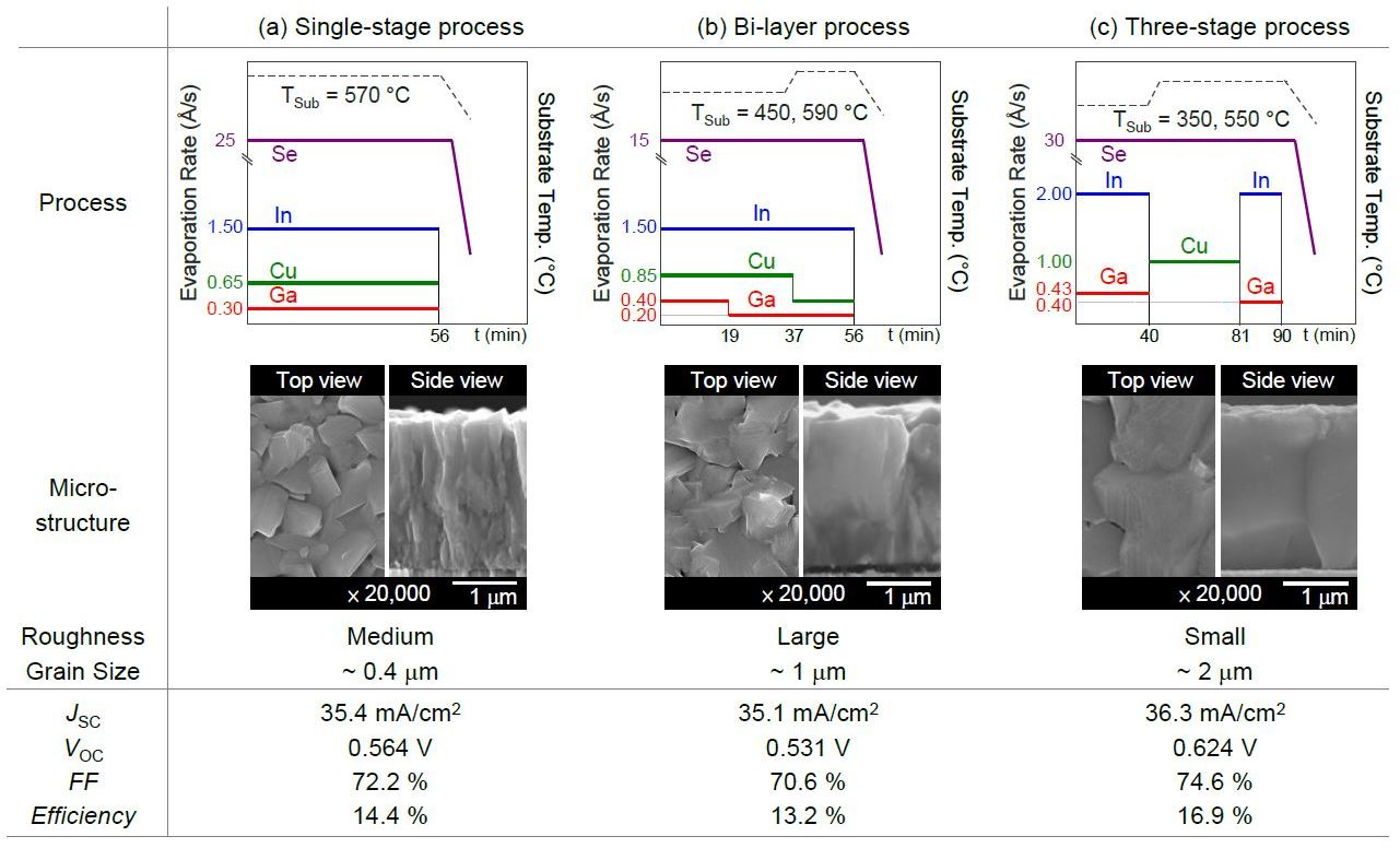
With respect to the co-evaporation methods, we employed various approaches including the single-stage, bi-layer, and three-stage processes to deposit the CIGS films. The graphic presentation of the co-evaporation processes for the profiles of the element flux rates and deposition temperatures are presented in Figure 6. In order to avoid the ambiguity caused by the composition issue, the compositions of the films deposited by various evaporation processes were maintained at the CGI ratio of around 0.88, and the thicknesses of the films were kept around 2 μm, as shown in Figure 6. The detailed deposition conditions of each process are exhibited. The Cu, In, Ga, and Se deposition rates and the substrate temperatures were remained constant for the single-stage process [28], as depicted in Figure 6a. The bi-layer process, which consists of two deposition stages, was developed by Boeing company [14,15]. As illustrated in Figure 6b, the Cu-rich film was deposited for the first stage, during which the grain growth could be enhanced. Sequentially, the Cu-poor film was then deposited to attain the overall composition of the slightly In-rich CIGS films. Not only can the large grain size of the as-deposited films be achieved, but also the composition of the films can be precisely controlled by varying the deposition time of the second stage. For the three-stage process [16], as displayed in Figure 6c, the InGaSe layers were initially formed as the solid foundation of the resulting CIGS films during the first stage. The films were then recrystallized and transformed into the CIGS films for the supply of the Cu and Se fluxes during the second stage until the overall composition of CIGS films became slightly Cu-rich. Finally, the InGaSe layers were deposited to compensate the Cu-rich compositions converting the films to the slightly In-rich chalcopyrite phases.
As illustrated in Figure 6, the compact and dense films were achieved for all evaporation processes. The XRD results indicated the strong (112) orientation followed by (204/220) and (116/312) orientations. No significant peaks of the second phases were found from the XRD results. The sharp XRD intensity of the CIGS films relative to that of the Mo layers exhibited that the as-deposited CIGS films had a favorite crystalline quality. The chalcopyrite structures of the as-deposited CIGS films were thus obtained. However, the films deposited with the different processes exhibited different microstructures. The corresponding SEM images of the surface morphologies and the cross-sectional views of the CIGS films are shown in Figure 6. In terms of the high-efficiency CIGS solar cells, the Cu-poor compositions of the CIGS films are required for the control of conductivity and carrier density of the CIGS films. However, the incorporation of the Cu-rich period during the deposition of CIGS films can enhance the grain growth, resulting in large grains. As shown in Figure 6, the CIGS films prepared by the bi-layer and three-stage processes had larger columnar grains than the CIGS films prepared by the single-stage process because the bi-layer and three-stage processes went through the Cu-rich period during the deposition processes. Although the grain sizes of the CIGS films deposited with the single-stage process were relatively small, the CIGS solar cells prepared by the single-stage process still outperformed the CIGS solar cells prepared by the bi-layer process in efficiencies, revealing that grain size is not a dominant factor impacting the efficiency of the CIGS solar cells.
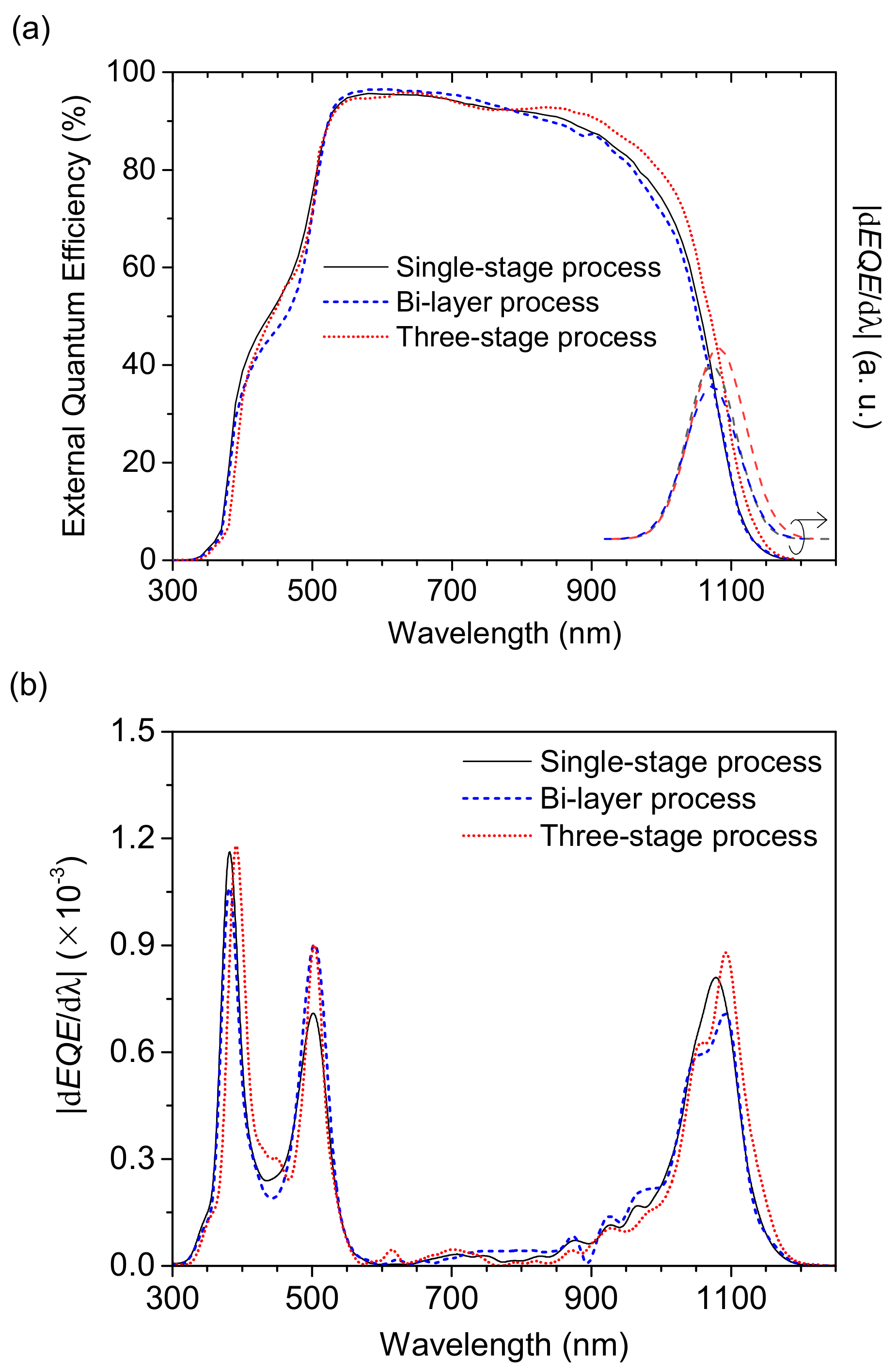
With the large optical absorption coefficients and the sufficient thicknesses for the CIGS films prepared by various co-evaporation processes, there was no significant difference in the short-circuit current densities of the CIGS solar cells in this study, as shown in Figure 6, but the short-circuit current density of the CIGS solar cell prepared by the three-stage process was still slightly greater than those of the cells prepared by the single-stage and bi-layer processes. In principle, the short-circuit current density can be estimated from the integral of the product of the incident photon flux and the external quantum efficiency (EQE). The short-circuit current density is directly related to the integral of the external quantum efficiency over the wavelength. Thus, the slight increase in the short-circuit current density of the CIGS solar cell prepared by the three-stage process could be attributed to the improvement of EQE in the long-wavelength region from approximately 800 nm to 1100 nm, as shown in Figure 7a.
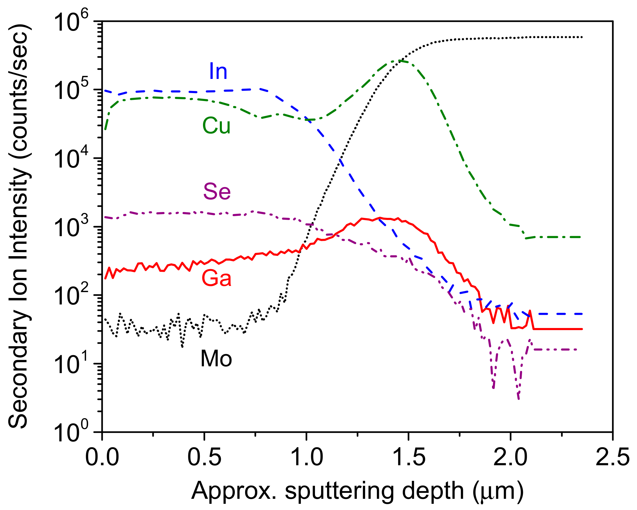
The optical absorption depth of the incident long-wavelength photons is longer than that of the short-wavelength photons. The long-wavelength photons are absorbed away from the space charge region of the CIGS solar cells. The minority carriers generated by the long-wavelength photons in the back region of the CIGS films have to count on the diffusion mechanism to be collected for the contribution to the current. With the Ga contents increased toward the back of the CIGS films prepared by three-stage process, as illustrated in Figure 8, the bandgap energies in the back region of the CIGS films increased. Thus, a quasi-electrical field [29] was established in the back region of the CIGS films, resulting in the formation of the back surface field (BSF) in the CIGS solar cells. Due to the creation of BSF, the back surface recombination was impeded and the effective diffusion length was enhanced, which were beneficial for carrier collection. Therefore, the cell prepared by the three-stage process had greater values of EQE than the other cells in the long-wavelength region from 800 nm to 1100 nm.
Figure 7b shows the absolute values of the first derivative of EQE with respect to the wavelength, namely |dEQE/dλ|. The bandgap energies of the CIGS films were estimated from the local maxima of |dEQE/dλ| [30,31,32]. The local maxima of |dEQE/dλ| determined by using a quadratic fit were at the wavelengths of 1072 nm, 1073 nm, and 1082 nm for the CIGS films prepared by the single-stage, bi-layer, and three-stage processes, respectively, as illustrated in Figure 7a [33]. The optical energies corresponding to the local maxima yield Eg + EU/2 [33,34], where EU is the Urbach energy. Taking the Urbach energy of around 20 meV for the CIGS films [20], the corresponding bandgap energies of the CIGS films prepared by the single-stage, bi-layer, and three-stage processes were 1.15 eV, 1.15 eV, and 1.14 eV, respectively. The bandgap energies of the CIGS films achieved by this method denote Eg,EQE, as shown in Table 3. In addition, the local maxima at the wavelengths of around 380 nm and 500 nm corresponding to the optical energies of 3.26 eV and 2.48 eV are the bandgap energies of ZnO:Al and CdS layers, respectively, where the ZnO:Al layers are the front contacts and the CdS layers are the buffers for the CIGS solar cells.
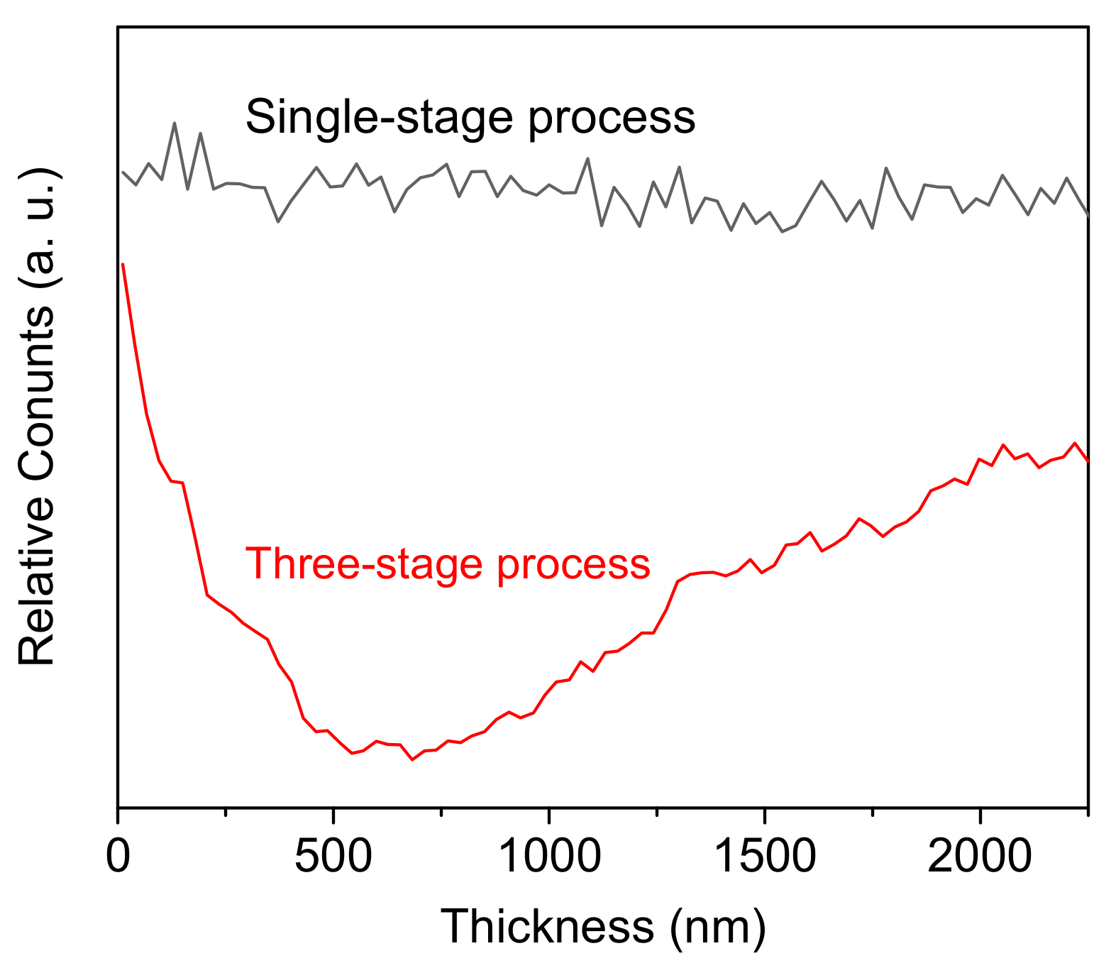
With similar GGI ratios for the CIGS films deposited by the co-evaporation processes, the corresponding bandgap energies are nearly the same. Nevertheless, the CIGS films prepared by the three-stage process had a double grading bandgap structure, meaning that the bandgap energies at the notch point of the V-shape grading structure had lower values than the effective optical bandgap energies [35,36,37]. Thus, the absorption edge of the CIGS films prepared by the three-stage process extended to the longer wavelengths than those of the films prepared by the other evaporation processes, as shown in Figure 7. With the effects of both improved carrier diffusion length and extended absorption edge, the CIGS solar cell prepared by the three-stage process had greater short-circuit current density than the cells prepared by the other co-evaporation processes, as presented in Figure 6.
As demonstrated in Figure 8, the non-uniform Ga distribution around the surface region of the CIGS films prepared by the three-stage process implemented the front grading bandgap structure for the CIGS solar cells, creating a barrier height for the electrons transporting from the CIGS layers to the buffers. The recombination rate in the SCR, which limits the open-circuit voltage of the CIGS solar cells, is reduced by increasing the barrier height for electrons via the increase in the bandgap in the SCR without a significant loss in the short-circuit current density. The formed barrier height created by the incorporation of high Ga content around the SCR suppressed the recombination rate between the CdS and CIGS layers, resulting in an increase in the open-circuit voltage.
The performance parameters, diode parameters, GGI ratios, and open-circuit voltage deficit (Eg/q-VOC) of CIGS solar cells prepared by the two-step and the co-evaporation processes are summarized in Table 3. The bandgap energies of Eg and Eg,EQE determined from the GGI ratios and the EQE results, respectively, are listed in Table 3.
For the extracted diode parameters presented in Table 3, the diode ideality factors ranged from 1.60 to 1.85, suggesting that the SCR recombination was dominant for these CIGS solar cells. The smaller diode ideality factor of the cell prepared by three-stage process demonstrated the reduced SCR recombination [38,39]. The diode current density based on the SCR recombination path can be described by [40]
The contribution of the SCR recombination to the diode current density depends on the parameters of the saturation current density and the diode ideality factor [41]. For the diode ideality factor of 1.60 to 1.69 for the cells prepared by the single-stage, bi-layer, and three-stage process, the decrease in the saturation current density suggests that the SCR recombination was reduced [42], and hence the junction quality of CIGS solar cells was enhanced [39]. The CIGS solar cell prepared by the three-stage process had the least saturation current density. Consequently, the open-circuit voltage of the CIGS solar cells prepared by three-stage process was greater than that of the cells prepared by the other co-evaporation processes, as shown in Table 3. On the other hand, since Ga was accumulated in the back of the CIGS film prepared by two-step process, the front region of the films turned into the compound of CuInSe2, whose bandgap energy was around 1.03 eV (Eg,EQE), resulting in the least open-circuit voltage and the greatest short-circuit current density. Furthermore, the large values of both the diode ideality factor and the saturation current density implied the low open-circuit voltage of the CIGS solar cells prepared by two-step process as well.
The best surface morphologies were achieved for the films deposited by the three-stage process, as the SEM images show in Figure 6. With the better surface morphologies of the CIGS films prepared by the three-stage process, a more conformal coverage of the buffers was achieved. The shunt resistance of the cells prepared by the three-stage process had the greatest values among the cells, as depicted in Table 3. In consequence, the leakage current and recombination current of the CIGS cells were effectively diminished, and the open-circuit voltage of the devices was improved. Thus, superior performance of the CIGS solar cells was attained. As shown in Figure 6, the dependence of the open-circuit voltage of the CIGS solar cells on the evaporation process is obvious. Both the surface morphologies and the grading bandgap structures are very crucial to the improvement of the open-circuit voltage of the CIGS solar cells.
To quantify the loss in the open-circuit voltage for the respective bandgap energies, the open-circuit voltage deficit was defined as the bandgap energy divided by electron charge and subtracted from the open-circuit voltage. The open-circuit voltage deficit can be given by [43,44]
where J00 is a prefactor which is proportional to the concentration N of recombination centers in the bulk of the CIGS film [43]. Therefore, the open-circuit voltage deficit decreased with the decrease of the diode ideality factor and the recombination centers. The least value of the diode ideality factor for the CIGS solar cell prepared by the three-stage process led to the smallest loss in the open-circuit voltage among the cells. On the contrary, the cell prepared by the two-step process with the greatest diode ideality factor had the largest open-circuit voltage deficit.
The dependence of fill factor on the series resistance, shunt resistance, and diode ideality factor is evident. The CIGS cell prepared by the three-stage process achieved low series resistance, high shunt resistance, and low diode ideality factor. In consequence, the cell had the greatest fill factor. Oppositely, the cell deposited by the two-step process had high series resistance, low shunt resistance, and high diode ideality factor, and thus a poor fill factor.
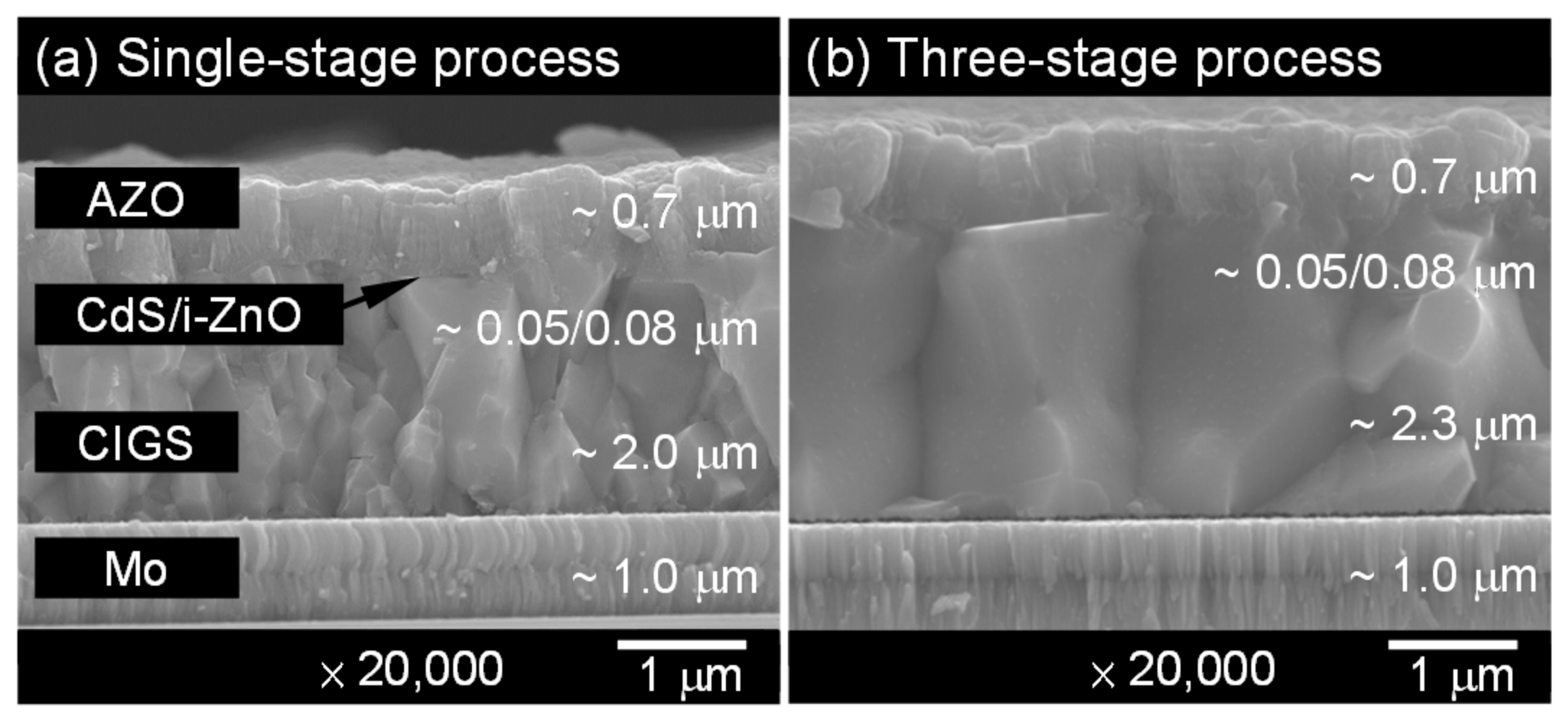
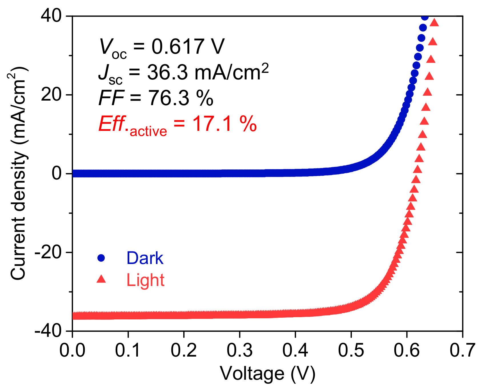
The cross-sectional views of the CIGS solar cells prepared by the single-stage and the three-stage processes are shown in Figure 9. Based on the deposition conditions given in Figure 6c, the deposition parameters of the three-stage process including the Ga distribution of the CIGS films were further optimized. With the Ga deposition rates of 0.5 Å/s and 0.4 Å/s for the first and the third stages, respectively, an active-area efficiency of 17.1% for the CIGS solar cells prepared by the three-stage process was achieved. The performance parameters of the CIGS solar cell have reached the open-circuit voltage of 0.617 V, short-circuit current density of 36.3 mA/cm2, and fill factor of 76.3%. The dark- and photo-J-V curves of this cell are illustrated in Figure 10. Further improvement of the open-circuit voltage for the as-fabricated CIGS solar cells should be achievable by fine tuning the optimal grading bandgap structures of the CIGS films and establishing the preferable electrical properties around the surface region of the CIGS films and the interface properties between the buffers and the CIGS films. More efforts spent on optimizing the co-evaporation process of the CIGS films and the CBD process of the buffers will be required in order to reach the goal of enhancing the open-circuit voltage of the CIGS solar cells, which are beyond the scope of this work.
In this work, a step-by-step approach to improve the performance of co-evaporated CIGS solar cells prepared by the single-stage and the three-stage process was demonstrated through tuning the critical compositions of the CIGS films prepared by the single-stage process and varying the Ga flux rates during the third stage of the three-stage. The diode parameters of the cells were extracted, and their correlations with the cell performance were analyzed. The mechanisms impacting the device characteristics of the CIGS solar cells prepared by different processes were discussed.
4. Summary and Conclusions
The two-step and the co-evaporation processes were employed to prepare the CIGS films. The effects of the process parameters on the properties of the CIGS films as well as the fabricated solar cells were investigated. For the two-step process, the impacts of the Se flow rates on the microstructural properties of the CIGS films with low or high Ga content were investigated. The CIGS films prepared at high Se flow rates exhibited improved surface morphology. It is concluded that the evaporated Se rate in vacuum during the two-step process plays a crucial role in determining the surface morphologies of the as-deposited CIGS films, and thus the performance, mainly the open-circuit voltage, of CIGS solar cells. An efficiency of 12.5% for the CIGS solar cells fabricated with the given process conditions has been achieved.
The effects of various co-evaporation processes including the single-stage, bi-layer, and three-stage processes on the properties of the CIGS films were studied. The compactness and chalcopyrite structures of the CIGS films were achieved for all of the evaporation processes. The grain growth of the CIGS films was improved via the incorporation of the Cu-rich period during the deposition of the bi-layer and three-stage processes. The grain sizes of the evaporated CIGS films were not a critical issue in influencing the performance of the CIGS solar cells. In terms of the surface morphologies, the three-stage process provided the better approach, leading to better coverage of the buffers. The grading bandgap structures of the CIGS films were implemented by means of Ga diffusion for the three-stage process, resulting in improvement of the open-circuit voltage and short-circuit current density for the CIGS solar cells. An efficiency of 17.1% for the CIGS solar cells prepared by the three-stage process has been achieved. In-depth analysis of the dominant factors controlling the performance parameters of the CIGS solar cells prepared by the two-step and various co-evaporation processes was presented.
Author Contributions
Funding acquisition, C.-H.H.; Investigation, C.-H.H., W.-J.C., C.-P.L., Y.-L.J. and Y.-C.S.; Methodology, C.-H.H. and C.-P.L.; Project administration, C.-H.H.; Resources, Y.-C.S.; Supervision, C.-H.H.; Visualization, W.-J.C.; Writing—original draft, C.-H.H.; Writing—review & editing, C.-H.H. and W.-J.C.
Funding
This research was funded by Ministry of Science and Technology (MOST), Taiwan under the contract number of 105-2221-E-259-023-MY2.
Acknowledgments
The authors would like to thank for the financial support of Ministry of Science and Technology (MOST), Taiwan under the contract number of 105-2221-E-259-023-MY2.
Conflicts of Interest
The authors declare no conflict of interest. The funders had no role in the design of the study; in the collection, analyses, or interpretation of data; in the writing of the manuscript, and in the decision to publish the results.
References
- Niki, S.; Contreras, M.; Repins, I.; Powalla, M.; Kushiya, K.; Ishizuka, S.; Matsubara, K. CIGS absorbers and processes. Prog. Photovolt. Res. Appl. 2010, 18, 453–466. [Google Scholar] [CrossRef]
- Repins, I.; Contreras, M.A.; Egaas, B.; DeHart, C.; Scharf, J.; Perkins, C.L.; To, B.; Noufi, R. 19.9%-efficient ZnO/CdS/CuInGaSe2 solar cell with 81.2% fill factor. Prog. Photovolt. Res. Appl. 2008, 16, 235–239. [Google Scholar] [CrossRef]
- Chirilǎ, A.; Reinhard, P.; Pianezzi, F.; Bloesch, P.; Uhl, A.R.; Fella, C.; Kranz, L.; Keller, D.; Gretener, C.; Hagendorfer, H.; et al. Potassium-induced surface modification of Cu(In,Ga)Se2 thin films for high-efficiency solar cells. Nat. Mater. 2013, 12, 1107–1111. [Google Scholar] [CrossRef] [PubMed]
- Jackson, P.; Hariskos, D.; Wuerz, R.; Kiowski, O.; Bauer, A.; Friedlmeier, T.M.; Powalla, M. Properties of Cu(In,Ga)Se2 solar cells with new record efficiencies up to 21.7%. Phys. Status Solidi-R. 2015, 9, 28–31. [Google Scholar] [CrossRef]
- Jackson, P.; Wuerz, R.; Hariskos, D.; Lotter, E.; Witte, W.; Powalla, M. Effects of heavy alkali elements in Cu(In,Ga)Se2 solar cells with efficiencies up to 22.6%. Phys. Status Solidi-R. 2016, 10, 583–586. [Google Scholar] [CrossRef]
- Green, M.A.; Hishikawa, Y.; Dunlop, E.D.; Levi, D.H.; Hohl-Ebinger, J.; Ho-Baillie, A.W.Y. Solar cell efficiency tables (version 52). Prog. Photovolt. Res. Appl. 2018, 26, 427–436. [Google Scholar] [CrossRef]
- Brown, G.; Stone, P.; Woodruff, J.; Cardozo, B.; Jackrel, D. Device characteristics of a 17.1% efficient solar cell deposited by a non-vacuum printing method on flexible foil. In Proceedings of the 38th IEEE Photovoltaic Specialists Conference, Austin, TX, USA, 3–8 June 2012; pp. 3230–3233. [Google Scholar]
- Aksu, S.; Pethe, S.; Kleiman-Shwarsctein, A.; Kundu, S.; Pinarbasi, M. Recent advances in electroplating based CIGS solar cell fabrication. In Proceedings of the 38th IEEE Photovoltaic Specialists Conference, Austin, TX, USA, 3–8 June 2012; pp. 3092–3097. [Google Scholar]
- Todorov, T.K.; Gunawan, O.; Gokmen, T.; Mitzi, D.B. Solution-processed Cu(In,Ga)(S,Se)2 absorber yielding a 15.2% efficient solar cell. Prog. Photovolt. Res. Appl. 2013, 21, 82–87. [Google Scholar] [CrossRef]
- Mazzer, M.; Rampino, S.; Gombia, E.; Bronzoni, M.; Bissoli, F.; Pattini, F.; Calicchio, M.; Kingma, A.; Annoni, F.; Calestani, D; et al. Progress on low-temperature pulsed electron deposition of CuInGaSe2 solar cells. Energies 2016, 9, 207. [Google Scholar] [CrossRef]
- Kato, T. Cu(In,Ga)(Se,S)2 solar cell research in Solar Frontier: Progress and current status. Jpn. J. Appl. Phys. 2017, 56. [Google Scholar] [CrossRef]
- Herrmann, D.; Kratzert, P.; Weeke, S.; Zimmer, M.; Djordjevic-Reiss, J.; Hunger, R.; Lindberg, P.; Wallin, E.; Lundberg, O.; Stolt, L. CIGS module manufacturing with high deposition rates and efficiencies. In Proceedings of the 40th IEEE Photovoltaic Specialist Conference, Denver, CO, USA, 8–13 June 2014; pp. 2775–2777. [Google Scholar]
- Dalibor, T.; Eraerds, P.; Grave, M.; Algasinger, M.; Visbeck, S.; Niesen, T.; Palm, J. Advanced PVD buffers on the road to GW-scale CIGSSe production. In Proceedings of the 43rd IEEE Photovoltaic Specialists Conference, Portland, OR, USA, 5–10 June 2016; pp. 1433–1437. [Google Scholar]
- Mickelsen, R.A.; Chen, W.S. Development of a 9.4% efficient thin-film CuInSe2/CdS solar cell. In Proceedings of the 15th IEEE Photovoltaic Specialists Conference, Kissimmee, FL, USA, 12–15 May 1981; pp. 800–804. [Google Scholar]
- Mickelsen, R.A.; Chen, W.S. Polycrystalline thin-film CuInSe2 solar cells. In Proceedings of the 16th IEEE Photovoltaic Specialists Conference, San Diego, CA, USA, 27–30 September 1982; pp. 781–785. [Google Scholar]
- Gabor, A.M.; Tuttle, J.R.; Albin, D.S.; Contreras, M.A.; Noufi, R.; Hermann, A.M. High-efficiency CuInxGa1−xSe2 solar cells made from (Inx,Ga1−x)2Se3 precursor films. Appl. Phys. Lett. 1994, 65, 198–200. [Google Scholar] [CrossRef]
- Hegedus, S.S.; Shafarman, W.N. Thin-film solar cells: Device measurements and analysis. Prog. Photovolt. Res. Appl. 2004, 12, 155–176. [Google Scholar] [CrossRef]
- Sites, J.R.; Mauk, P.H. Diode quality factor determination for thin-film solar cells. Sol. Cells 1989, 27, 411–417. [Google Scholar] [CrossRef]
- Lundberg, O.; Edoff, M.; Stolt, L. The effect of Ga-grading in CIGS thin film solar cells. Thin Solid Films 2005, 480–481, 520–525. [Google Scholar] [CrossRef]
- Heath, J.T.; Cohen, J.D.; Shafarman, W.N.; Liao, D.X.; Rockett, A.A. Effect of Ga content on defect states in CuIn1−xGaxSe2 photovoltaic devices. Appl. Phys. Lett. 2002, 80, 4540–4542. [Google Scholar] [CrossRef]
- Pudov, A.O.; Sites, J.R.; Contreras, M.A.; Nakada, T.; Schock, H.-W. CIGS J-V distortion in the absence of blue photons. Thin Solid Films 2005, 480–481, 273–278. [Google Scholar] [CrossRef]
- Cao, Q.; Gunawan, O.; Copel, M.; Reuter, K.B.; Chey, S.J.; Deline, V.R.; Mitzi, D.B. Defects in Cu(In,Ga)Se2 chalcopyrite semiconductors: A comparative study of material properties, defect states, and photovoltaic performance. Adv. Energy Mater. 2011, 1, 845–853. [Google Scholar] [CrossRef]
- Kamada, R.; Shafarman, W.N.; Birkmire, R.W. Cu(In,Ga)Se2 film formation from selenization of mixed metal/metal-selenide precursors. Sol. Energy Mater. Sol. Cells 2010, 94, 451–456. [Google Scholar] [CrossRef]
- Hanket, G.M.; Kamada, R.; Kim, W.K.; Shafarman, W.N. Effect of reaction temperature on Cu(InGa)(SeS)2 formation by a sequential H2Se/H2S precursor reaction process. In Proceedings of the 33rd IEEE Photovoltaic Specialists Conference, San Diego, CA, USA, 11–16 May 2008; pp. 1–5. [Google Scholar]
- Delsol, T.; Samantilleke, A.P.; Chaure, N.B.; Gardiner, P.H.; Simmonds, M.; Dharmadasa, I.M. Experimental study of graded bandgap Cu(InGa)(SeS)2 thin films grown on glass/molybdenum substrates by selenization and sulphidation. Sol. Energy Mater. Sol. Cells 2004, 82, 587–599. [Google Scholar] [CrossRef]
- Marudachalam, M.; Birkmire, R.W.; Hichri, H.; Schultz, J.M.; Swartzlander, A.; Al-Jassim, M.M. Phases, morphology, and diffusion in CulnxGa1−xSe2 thin films. J. Appl. Phys. 1997, 82, 2896–2905. [Google Scholar] [CrossRef]
- Haalboom, T.; Gödecke, T.; Ernst, F.; Rühle, M.; Herberholz, R.; Schock, H.-W.; Beilharz, C.; Benz, K. Phase relations and microstructure in bulk materials and thin films of the ternary system Cu-In-Se. In Proceedings of the 11th ternary and multinary compounds, Salford, UK, 8–12 September 1997; IOP Publishing: Bristol, UK, 1998; pp. 249–252. [Google Scholar]
- Huang, C.-H.; Lin, C.-P.; Jan, Y.-L. Characteristics of CIGS photovoltaic devices co-evaporated with various Se flux rates at low temperatures. Semicond. Sci. Tech. 2016, 31, 085004. [Google Scholar] [CrossRef]
- Kroemer, H. Quasi-electric and quasi-magnetic fields in nonuniform semiconductors. RCA Rev. 1957, 18, 332–342. [Google Scholar]
- Kim, K.; Park, H.; Hanket, G.M.; Kim, W.K.; Shafarman, W.N. Composition and bandgap control in Cu(In,Ga)Se2-based absorbers formed by reaction of metal precursors. Prog. Photovolt. Res. Appl. 2015, 23, 765–772. [Google Scholar] [CrossRef]
- Yang, J.Y.; Lee, D.H.; Huh, K.S.; Jung, S.J.; Lee, J.W.; Lee, H.C.; Baek, D.H.; Kim, B.J.; Kim, D.S.; Nam, J.G.; et al. Influence of surface properties on the performance of Cu(In,Ga)(Se,S)2 thin-film solar cells using kelvin probe force microscopy. RSC Adv. 2015, 5, 40719–40725. [Google Scholar] [CrossRef]
- Chantana, J.; Kato, T.; Sugimoto, H.; Minemoto, T. Investigation of correlation between open-circuit voltage deficit and carrier recombination rates in Cu(In,Ga)(S,Se)2-based thin-film solar cells. Appl. Phys. Lett. 2018, 112, 151601. [Google Scholar] [CrossRef]
- Mansfield, L.M.; Garris, R.L.; Counts, K.D.; Sites, J.R.; Thompson, C.P.; Shafarman, W.N.; Ramanathan, K. Comparison of CIGS solar cells made with different structures and fabrication techniques. IEEE J. Photovolt. 2017, 7, 286–293. [Google Scholar] [CrossRef]
- Hages, C.J.; Carter, N.J.; Agrawal, R. Generalized quantum efficiency analysis for non-ideal solar cells: Case of Cu2ZnSnSe4. J. Appl. Phys. 2016, 119, 014505. [Google Scholar] [CrossRef]
- Contreras, M.A.; Tuttle, J.; Gabor, A.; Tennant, A.; Ramanathan, K.; Asher, S.; Franz, A.; Keane, J.; Wang, L.; Scofield, J.; et al. High efficiency Cu(In,Ga)Se2-based solar cells: Processing of novel absorber structures. In Proceedings of the 1st World Conference on Photovoltaic Energy Conversion, Waikoloa, HI, USA, 5–9 December 1994; pp. 68–75. [Google Scholar]
- Topič, M.; Smole, F.; Furlan, J. Band-gap engineering in CdS/Cu(In,Ga)Se2 solar cells. J. Appl. Phys. 1996, 79, 8537–8540. [Google Scholar] [CrossRef]
- Gabor, A.M.; Tuttle, J.R.; Bode, M.H.; Franz, A.; Tennant, A.L.; Contreras, M.A.; Noufi, R.; Jensen, D.G.; Hermann, A.M. Band-gap engineering in Cu(In,Ga)Se2 thin films grown from (In,Ga)2Se3 precursors. Sol. Energy Mater. Sol. Cells 1996, 41–42, 247–260. [Google Scholar] [CrossRef]
- Contreras, M.A.; Egaas, B.; Ramanathan, K.; Hiltner, J.; Swartzlander, A.; Hasoon, F.; Noufi, R. Progress toward 20% efficiency in Cu(In,Ga)Se2 polycrystalline thin-film solar cells. Prog. Photovolt. Res. Appl. 1999, 7, 311–316. [Google Scholar] [CrossRef]
- Contreras, M.A.; Romero, M.J.; Noufi, R. Characterization of Cu(In,Ga)Se2 materials used in record performance solar cells. Thin Solid Films 2006, 511–512, 51–54. [Google Scholar] [CrossRef]
- Phillips, J.E.; Birkmire, R.W.; McCandless, B.E.; Meyers, P.V.; Shafarman, W.N. Polycrystalline heterojunction solar cells: A device perspective. Phys. Status Solidi B 1996, 194, 31–39. [Google Scholar] [CrossRef]
- Scheer, R.; Schock, H.-W. Thin Film Heterostructures. In Chalcogenide Photovoltaics: Physics, Technologies, and Thin Film Devices; Wiley-VCH: Weinheim, Germany, 2011; p. 38. ISBN 978-352-731-459-1. [Google Scholar]
- Contreras, M.A.; Ramanathan, K.; AbuShama, J.; Hasoon, F.; Young, D.L.; Egaas, B.; Noufi, R. Diode characteristics in state-of-the-art ZnO/CdS/Cu(In1−xGax)Se2 solar cells. Prog. Photovolt. Res. Appl. 2005, 13, 209–216. [Google Scholar] [CrossRef]
- Rau, U.; Jasenek, A.; Schock, H.W.; Engelhardt, F.; Meyer, T. Electronic loss mechanisms in chalcopyrite based heterojunction solar cells. Thin Solid Films 2000, 361, 298–302. [Google Scholar] [CrossRef]
- Hanna, G.; Jasenek, A.; Rau, U.; Schock, H.W. Influence of the Ga-content on the bulk defect densities of Cu(In,Ga)Se2. Thin Solid Films 2001, 387, 71–73. [Google Scholar] [CrossRef]
Figure 1.
(a) Temperature profile of metal precursors during selenization for two-step process, (b) J-V characteristics of a CIGS solar cell prepared by the two-step process, (c) the derivative of dJ/dV for the determination of the shunt characteristics, (d) the derivative of dV/dJ in forward bias with fit used to determine the series resistance and the diode ideality factor, and (e) ln(J + JSC − GV) with fit used to determine the reverse saturation current density and the diode ideality factor. (Eff. and Eff.active denote the total-area efficiency and active-area efficiency, respectively).
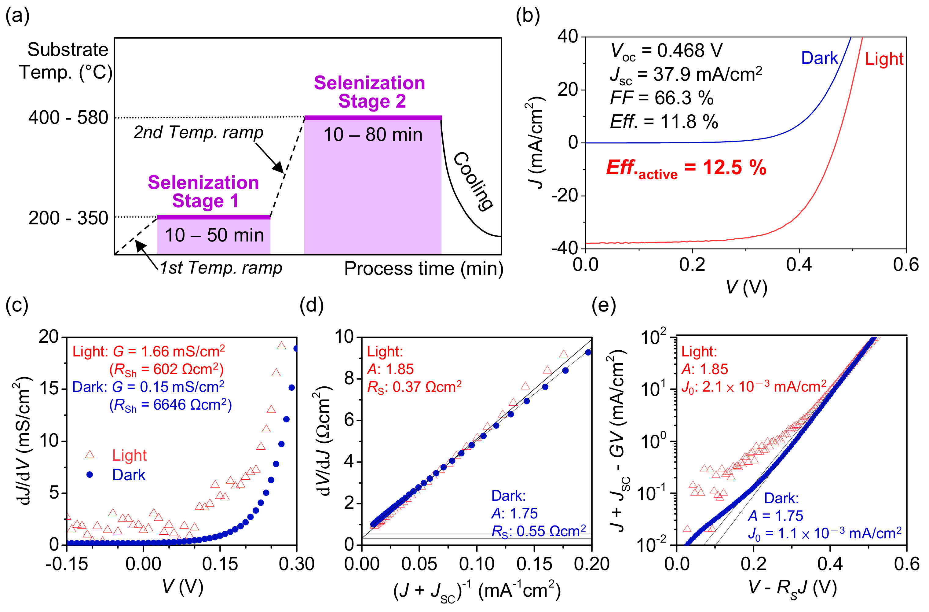
Figure 2.
SEM micrographs of surface morphologies of CIGS films with (a) low and (b) high Ga content selenized at low Se flow rate (15 Å/s), and of CIGS films (c) low and (d) high Ga content selenized at high Se flow rate (25 Å/s).
Figure 2.
SEM micrographs of surface morphologies of CIGS films with (a) low and (b) high Ga content selenized at low Se flow rate (15 Å/s), and of CIGS films (c) low and (d) high Ga content selenized at high Se flow rate (25 Å/s).
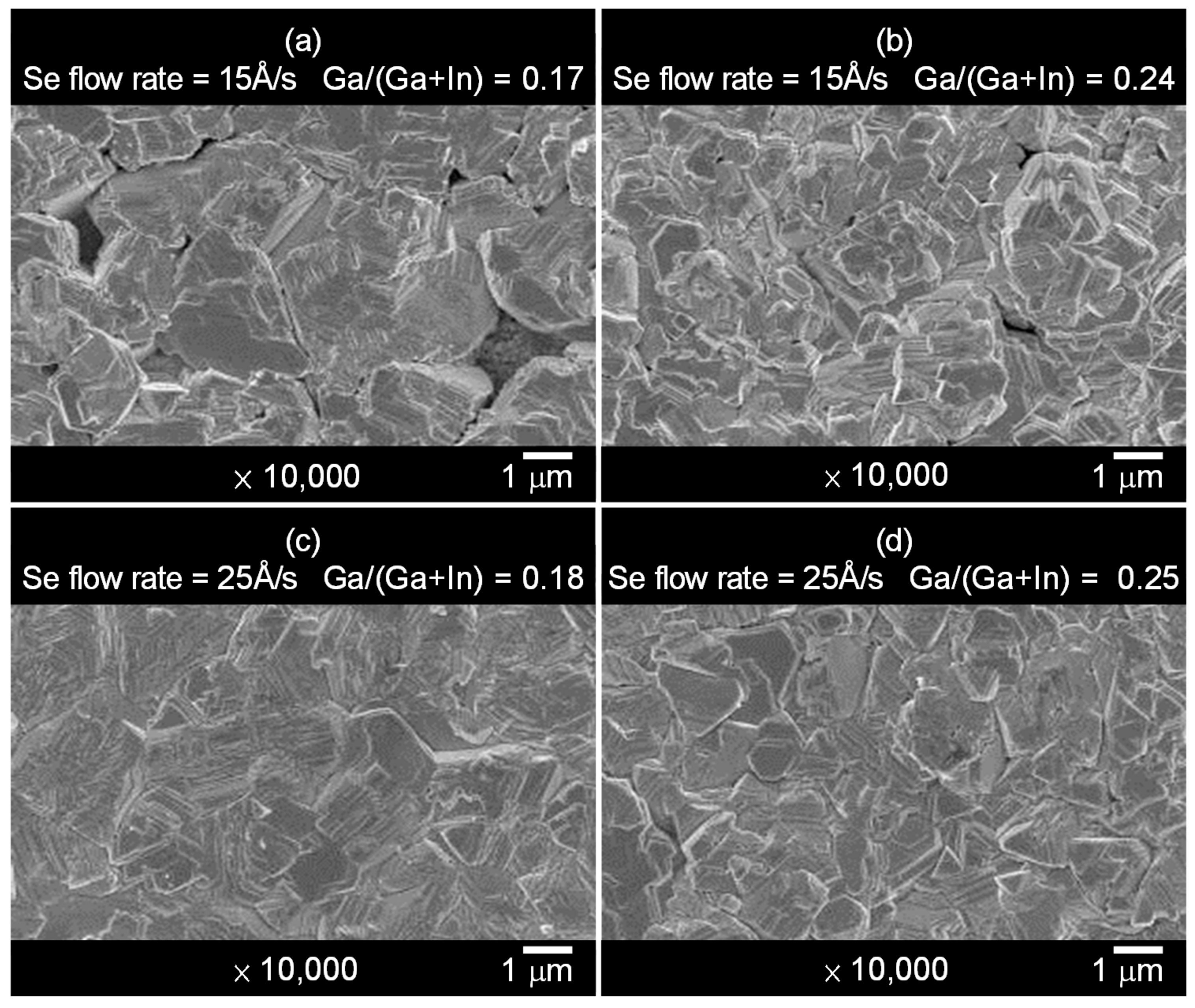
Figure 3.
(a) SEM cross-sectional view of CBD CdS buffer layer on a CIGS film, and (b) SEM cross-sectional view of a CIGS solar cell prepared by the two-step process.
Figure 3.
(a) SEM cross-sectional view of CBD CdS buffer layer on a CIGS film, and (b) SEM cross-sectional view of a CIGS solar cell prepared by the two-step process.
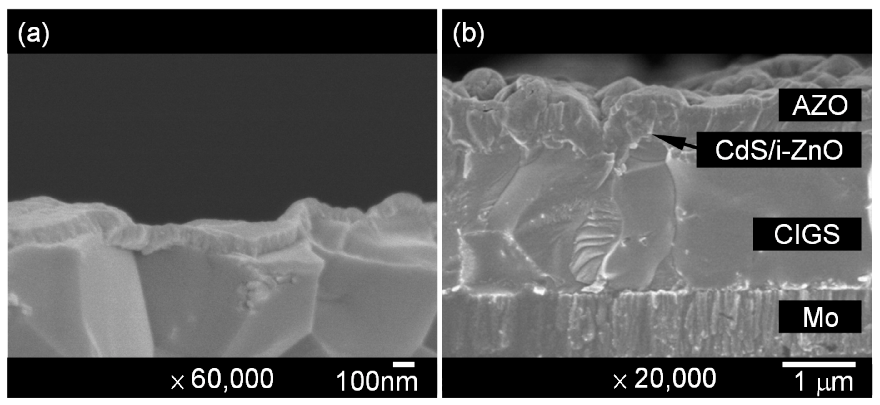
Figure 4.
SIMS depth profile of CIGS film with a Ga/(Ga + In) ratio of 0.25 selenized at the Se flow rate of 25 Å/s.
Figure 4.
SIMS depth profile of CIGS film with a Ga/(Ga + In) ratio of 0.25 selenized at the Se flow rate of 25 Å/s.

Figure 5.
Dependence of performance parameters on CGI and GGI ratios of CIGS films prepared by the single-stage process.
Figure 5.
Dependence of performance parameters on CGI and GGI ratios of CIGS films prepared by the single-stage process.
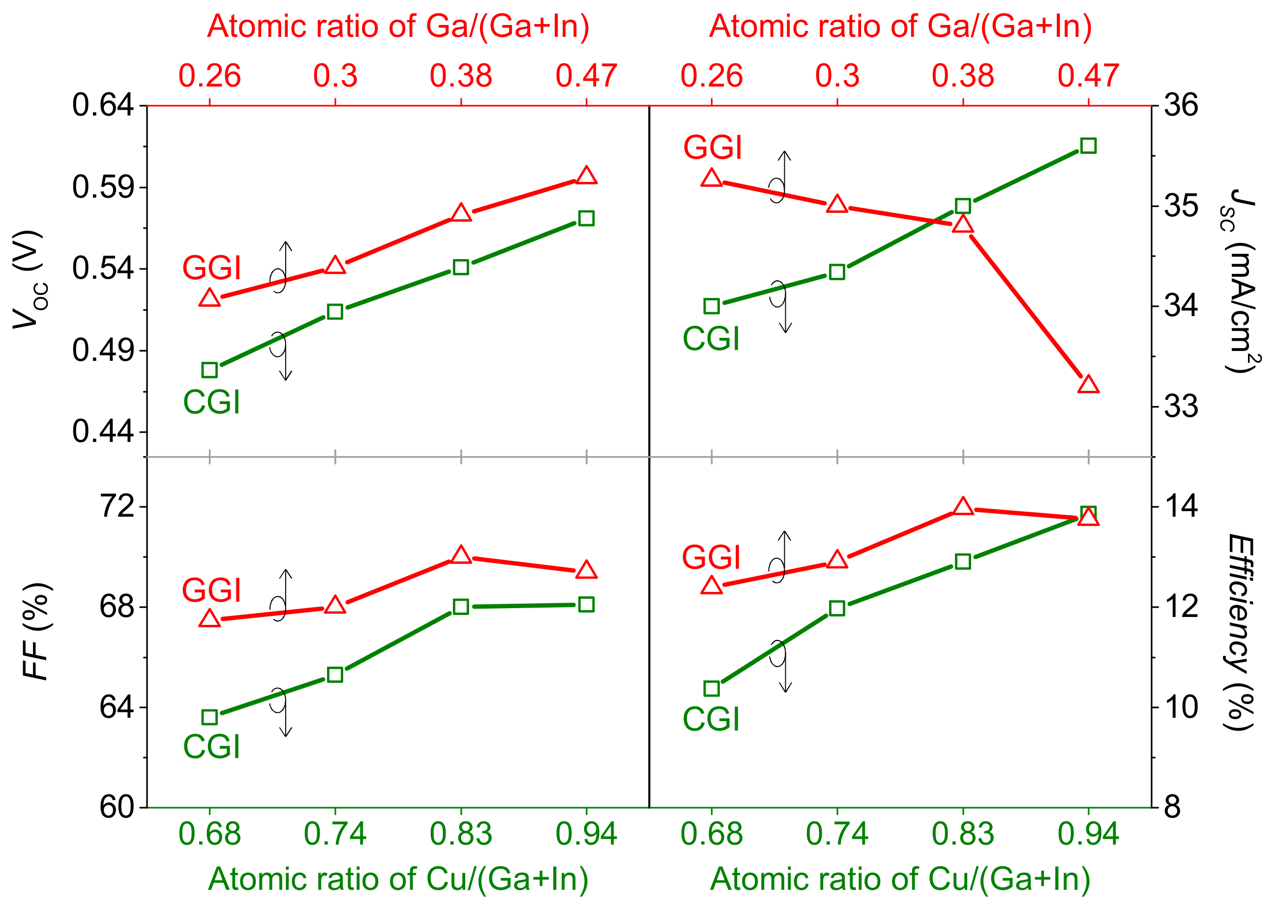
Figure 6.
(a) Graphic presentation of single-stage process parameters, SEM micrographs of surface morphologies, and cross-sectional views of CIGS films prepared by single-stage process, and performance parameters, (b) Graphic presentation of bi-layer process parameters, SEM micrographs of surface morphologies, and cross-sectional views of CIGS films prepared by the bi-layer process, and performance parameters, and (c) Graphic presentation of three-stage process parameters, SEM micrographs of surface morphologies, and cross-sectional views of CIGS films prepared by the three-stage process, and performance parameters.

Figure 7.
(a) External quantum efficiencies of CIGS solar cells prepared by the single-stage, bi-layer, and three-stage processes, and (b) the absolute values of d(EQE)/dλ as a function of wavelength.
Figure 7.
(a) External quantum efficiencies of CIGS solar cells prepared by the single-stage, bi-layer, and three-stage processes, and (b) the absolute values of d(EQE)/dλ as a function of wavelength.

Figure 8.
SIMS depth profiles of Ga distribution for the CIGS films prepared by the single-stage and three-stage processes.
Figure 8.
SIMS depth profiles of Ga distribution for the CIGS films prepared by the single-stage and three-stage processes.

Figure 9.
SEM cross-sectional views of CIGS solar cells prepared by (a) the single-stage process and (b) the three-stage process.
Figure 9.
SEM cross-sectional views of CIGS solar cells prepared by (a) the single-stage process and (b) the three-stage process.

Figure 10.
J-V characteristics of the CIGS solar cell prepared by the three-stage process.


Table 1.
Composition ratios and performance parameters of CIGS solar cells with (a) low and (b) high Ga contents selenized at low Se flow rate (15 Å/s), and of CIGS solar cells with (c) low and (d) high Ga contents selenized at high Se flow rate (25 Å/s).
Table 1.
Composition ratios and performance parameters of CIGS solar cells with (a) low and (b) high Ga contents selenized at low Se flow rate (15 Å/s), and of CIGS solar cells with (c) low and (d) high Ga contents selenized at high Se flow rate (25 Å/s).
| Sample No. | Se Flow Rate | Composition (at %) | Cu/(Ga + In) | Ga/(Ga + In) | VOC (V) | JSC (mA/cm2) | FF (%) | η (%) | |||
|---|---|---|---|---|---|---|---|---|---|---|---|
| Cu | In | Ga | Se | ||||||||
| (a) | 15 Å/s | 21.9 | 23.1 | 4.8 | 50.2 | 0.79 | 0.17 | 0.432 | 39.0 | 62.2 | 10.5 |
| (b) | 15 Å/s | 22.8 | 21.0 | 6.7 | 49.5 | 0.82 | 0.24 | 0.451 | 38.6 | 64.5 | 11.2 |
| (c) | 25 Å/s | 21.4 | 22.6 | 5.1 | 50.9 | 0.77 | 0.18 | 0.452 | 40.1 | 64.7 | 11.7 |
| (d) | 25 Å/s | 22.2 | 19.7 | 6.6 | 51.5 | 0.84 | 0.25 | 0.468 | 40.1 | 66.3 | 12.5 |
Table 2.
Performance parameters of CIGS solar cells prepared by the three-stage process with various Ga flux rates during the third stage.
Table 2.
Performance parameters of CIGS solar cells prepared by the three-stage process with various Ga flux rates during the third stage.
| Ga Flux Rate | VOC (V) | JSC (mA/cm2) | FF (%) | η (%) | RSh (Ωcm2) | RSh (Ωcm2) | A | J0 (mA/cm2) |
|---|---|---|---|---|---|---|---|---|
| 0.40 Å/s | 0.593 | 35.5 | 71.4 | 14.9 | 0.18 | 1304 | 1.64 | 2.2 × 10⁻⁵ |
| 0.45 Å/s | 0.597 | 35.4 | 72.1 | 15.2 | 0.08 | 1326 | 1.61 | 1.5 × 10⁻⁵ |
| 0.50 Å/s | 0.604 | 35.2 | 72.6 | 15.4 | 0.09 | 1345 | 1.61 | 1.3 × 10⁻⁵ |
| 0.55 Å/s | 0.598 | 35.1 | 71.8 | 15.1 | 0.09 | 1352 | 1.63 | 1.9 × 10⁻⁵ |
Table 3.
Performance parameters, diode parameters, GGI ratios, bandgap energies (Eg and Eg,EQE), and open-circuit voltage deficit (Eg/q-VOC) of CIGS solar cells prepared by the two-step, single-stage, bi-layer, and three-stage processes.
Table 3.
Performance parameters, diode parameters, GGI ratios, bandgap energies (Eg and Eg,EQE), and open-circuit voltage deficit (Eg/q-VOC) of CIGS solar cells prepared by the two-step, single-stage, bi-layer, and three-stage processes.
| Process | VOC (V) | JSC (mA/cm2) | FF (%) | η (%) | RS (Ωcm2) | RSh (Ωcm2) | A | J0 (mA/cm2) | GGI | Eg (eV) | Eg,EQE (eV) | Eg/q-VOC (V) |
|---|---|---|---|---|---|---|---|---|---|---|---|---|
| Two-step | 0.468 | 40.1 | 66.3 | 12.5 | 0.37 | 602 | 1.85 | 2.1 × 10⁻³ | 0.25 | 1.14 | 1.03 | 0.672 |
| Single-stage | 0.564 | 35.4 | 72.2 | 14.4 | 0.06 | 1269 | 1.64 | 5.0 × 10⁻⁵ | 0.28 | 1.16 | 1.15 | 0.596 |
| Bi-layer | 0.531 | 35.1 | 70.6 | 13.2 | 0.11 | 1190 | 1.69 | 1.7 × 10⁻⁴ | 0.24 | 1.14 | 1.15 | 0.609 |
| Three-stage | 0.624 | 36.3 | 74.6 | 16.9 | 0.06 | 1572 | 1.60 | 9.1 × 10⁻⁶ | 0.30 | 1.17 | 1.14 | 0.546 |
© 2018 by the authors. Licensee MDPI, Basel, Switzerland. This article is an open access article distributed under the terms and conditions of the Creative Commons Attribution (CC BY) license (http://creativecommons.org/licenses/by/4.0/).
Share and Cite
MDPI and ACS Style
Huang, C.-H.; Chuang, W.-J.; Lin, C.-P.; Jan, Y.-L.; Shih, Y.-C. Deposition Technologies of High-Efficiency CIGS Solar Cells: Development of Two-Step and Co-Evaporation Processes. Crystals 2018, 8, 296. https://doi.org/10.3390/cryst8070296
AMA Style
Huang C-H, Chuang W-J, Lin C-P, Jan Y-L, Shih Y-C. Deposition Technologies of High-Efficiency CIGS Solar Cells: Development of Two-Step and Co-Evaporation Processes. Crystals. 2018; 8(7):296. https://doi.org/10.3390/cryst8070296
Chicago/Turabian StyleHuang, Chia-Hua, Wen-Jie Chuang, Chun-Ping Lin, Yueh-Lin Jan, and Yu-Chiu Shih. 2018. "Deposition Technologies of High-Efficiency CIGS Solar Cells: Development of Two-Step and Co-Evaporation Processes" Crystals 8, no. 7: 296. https://doi.org/10.3390/cryst8070296
Note that from the first issue of 2016, this journal uses article numbers instead of page numbers. See further details here.