Progress in Contact, Doping and Mobility Engineering of MoS2: An Atomically Thin 2D Semiconductor
by
 , ,
, ,
Amritesh Rai
* ,
,
Hema C. P. Movva
,
Anupam Roy
,
Deepyanti Taneja
,
Sayema Chowdhury
and
Sanjay K. Banerjee
Microelectronics Research Center, Department of Electrical and Computer Engineering, The University of Texas at Austin, Austin, TX 78758, USA
*
Author to whom correspondence should be addressed.
Crystals 2018, 8(8), 316; https://doi.org/10.3390/cryst8080316
Submission received: 30 January 2018
/
Revised: 19 May 2018
/
Accepted: 19 May 2018
/
Published: 6 August 2018
(This article belongs to the Special Issue Integration of 2D Materials for Electronics Applications)
Abstract
:Atomically thin molybdenum disulfide (MoS2), a member of the transition metal dichalcogenide (TMDC) family, has emerged as the prototypical two-dimensional (2D) semiconductor with a multitude of interesting properties and promising device applications spanning all realms of electronics and optoelectronics. While possessing inherent advantages over conventional bulk semiconducting materials (such as Si, Ge and III-Vs) in terms of enabling ultra-short channel and, thus, energy efficient field-effect transistors (FETs), the mechanically flexible and transparent nature of MoS2 makes it even more attractive for use in ubiquitous flexible and transparent electronic systems. However, before the fascinating properties of MoS2 can be effectively harnessed and put to good use in practical and commercial applications, several important technological roadblocks pertaining to its contact, doping and mobility (µ) engineering must be overcome. This paper reviews the important technologically relevant properties of semiconducting 2D TMDCs followed by a discussion of the performance projections of, and the major engineering challenges that confront, 2D MoS2-based devices. Finally, this review provides a comprehensive overview of the various engineering solutions employed, thus far, to address the all-important issues of contact resistance (RC), controllable and area-selective doping, and charge carrier mobility enhancement in these devices. Several key experimental and theoretical results are cited to supplement the discussions and provide further insight.
Contents
| 1. Introduction…………………………………………………………………………………………. [3] |
| 2. Projected Performance of 2D MoS2……………………………………………………………… [5] |
| 3. Major Challenges in Contact, Doping and Mobility Engineering of 2D MoS2………...… [7] |
| 3.1. The Schottky Barrier and the van der Waals (vdW) Gap………………………………………...[7] |
| 3.2. Contact Length Scaling, Doping and Extrinsic Carrier Scattering……………………………..[10] |
| 3.3. Tackling the Major Challenges…………………………………………………………………... [11] |
| 4. Contact Work Function Engineering…………………………………………………….….…....[11] |
| 4.1. N-Type Work Function Engineering……………………………………………………………. [12] |
| 4.2. P-Type Work Function Engineering…………………………………………………………….. [14] |
| 5. Effect of Stoichiometry, Contact Morphology and Deposition Conditions……………….. [14] |
| 6. Electric Double Layer (EDL) Gating……………………………………….…………………….. [16] |
| 7. Surface Charge Transfer Doping.…….………………………………………………………….. [18] |
| 7.1. Charge Transfer Electron Doping……………………………………………………………….. [19] |
| 7.2. Charge Transfer Hole Doping…………………………………………………………………… [21] |
| 8. Use of Interfacial Contact ‘Tunnel’ Barriers……………………………………………………. [23] |
| 9. Graphene 2D Contacts to MoS2………………………………………………………………….. [26] |
| 10. Effects of MoS2 Layer Thickness……………………………………………………………….. [30] |
| 11. Effects of Contact Architecture (Top versus Edge)…………………………………………... [34] |
| 12. Hybridization and Phase Engineering……………………………………………………........ [37] |
| 13. Engineering Structural Defects, Interface Traps and Surface States………………..…...... [40] |
| 14. Role of Dielectrics in Doping and Mobility Engineering……………………….………….. [44] |
| 14.1. Dielectrics as Dopants………………………………………………………………………….. [45] |
| 14.2. Mobility Engineering with Dielectrics: Role of High-κ………………………………………...[47] |
| 14.3. Limitations of High-κ Dielectrics and Advantages of Nitride Dielectric Environments……... [50] |
| 15. Substitutional Doping of 2D MoS2…………………………………………………………….. [55] |
| 15.1. Hole Doping by Cation Substitution…………………………………………………………… [57] |
| 15.2. Electron Doping by Cation Substitution……………………………………………………….. [58] |
| 15.3. Electron and Hole Doping by Anion Substitution……………………………………………... [59] |
| 15.4. Towards Controlled and Area-Selective Substitutional Doping………………….…………..... [62] |
| 16. Conclusions and Future Outlook………………………………………………………………... [64] |
1. Introduction
The isolation and characterization of graphene, an atomically thin layer of carbon atoms arranged in a hexagonal lattice, in 2004 by Geim and Novoselov ushered in the era of two-dimensional (2D) atomically thin layered materials [1]. This all-important discovery came at the backdrop of a continuous ongoing quest by the semiconductor industry to search for new semiconducting materials, engineering techniques and efficient transistor topologies to extend “Moore’s Law”—an observation made in the 1960s by Gordon Moore which stated that the number of transistors on a complementary metal-oxide-semiconductor (CMOS) microprocessor chip and, hence, the chip’s performance, would double every two years or so [2,3,4]. In effect, this law led to the shrinking down of conventional CMOS transistors (down into the nm regime) to enhance their density and performance on the chip [5,6,7,8,9,10]. However, in the past decade or so, the performance gains derived due to dimensional scaling have been severely offset by the detrimental short-channel effects (SCE) that cause high OFF-state leakage currents (due to loss of effective gate control over the charge carriers in the semiconducting channel and inability of the gate to turn the channel fully OFF) leading to higher static power consumption and heat dissipation (i.e., wasted power), which have dire implications for Moore’s Law [11,12,13,14,15,16]. With continued scaling (sub-10 nm regime), the SCE effect will get far worse and even state-of-the-art CMOS transistor architectures designed to enhance gate controllability (such as MuGFETs, UTB-FETs, FinFETs, etc.) will face serious challenges in minimizing the overall power consumption. Hence, the need of the hour is an appropriate transistor channel material that allows for a high degree of gate controllability at these ultra-short dimensions [17,18,19,20]. In this light, graphene has been thoroughly researched for its remarkable properties, such as 2D atomically thin nature, extremely high carrier mobilities, superior mechanical strength, flexibility, optical transparency, and high thermal conductivity, that can be useful for a wide range of device applications [21,22,23]. While graphene can allow for excellent gate controllability due to its innate atomic thickness, a major drawback of graphene is its “semi-metallic” nature and, hence, the absence of an electronic “band-gap” (Eg)—a necessary attribute any material must possess to be considered for electronic/optoelectronic device applications. Hence, a graphene transistor cannot be turned “OFF” [24,25].
Graphene’s shortcomings led to the search for alternative materials with similar yet complementary properties. This led to the emergence of a laundry list of 2D layered materials ranging from insulators to semiconductors and metals [26,27]. Among these 2D materials, the family of transition metal dichalcogenides (TMDCs) has garnered the most attention [28]. These TMDCs are characterized by the general formula MX2 where M represents a transition metal (M = Mo, W, Re, etc.) and X is a chalcogen (X = S, Se, Te) [29,30]. Analogous to graphene, these layered 2D TMDCs can be isolated down to a single atomic layer from their bulk form. A TMDC monolayer can be visualized as a layer of transition metal atoms sandwiched in-between two layers of chalcogen atoms (of the form X-M-X) with strong intra-layer covalent bonding, whereas the inter-layer bonding between two adjacent TMDC layers is of the van der Waals (vdW) type (Figure 1a schematically illustrates the 3D crystal structure of molybdenum disulfide or MoS2, the prototypical TMDC). Moreover, depending on the specific crystal structure and atomic layer stacking sequence (1T, 2H or 3R), these TMDCs can have metallic, semiconducting or superconducting phases [29,30]. Of particular interest is the subset of semiconducting 2D TMDCs as they offer several promising advantages over conventional 3D semiconductors (Si, Ge and III-Vs) such as: (i) inherent ultra-thin bodies enabling enhanced electrostatic gate control and carrier confinement versus 3D bulk semiconductors (this can help mitigate SCE in ultra-scaled FETs based on 2D TMDCs as their ultra-thin bodies can allow significant reduction of the so-called characteristic “channel length (LCH) scaling” factor “λ”, given by λ = √(tOXtBODYεBODY)/εOX, where tOX and tBODY are the thicknesses of the gate oxide and channel, respectively, and εOX and εBODY are their respective dielectric constants; a simple relationship for the scaling limit of FETs, i.e., minimum length required to prevent SCE, is given by LCH > 3λ) (Figure 1c shows the schematic cross sections of the gate-channel regions of FETs employing bulk 3D and 2D semiconducting channels and compares their electrostatic carrier confinements) [31]; (ii) availability of a wide range of sizeable band-gaps and diverse band-alignments [32]; and (iii) lack of surface “dangling bonds” unlike conventional 3D semiconductors (Figure 1b schematically compares the surface of bulk 3D and 2D materials) allowing for the formation of pristine defect-free interfaces (especially 2D/2D vdW interfaces) [33]. These attributes make the semiconducting 2D TMDCs extremely promising for future “ultra-scaled” and “ultra-low-power” devices [30,31,33,34,35,36,37,38,39]. Among the semiconducting 2D TMDCs, MoS2 has been the most popular and widely pursued material by the research community owing to its natural availability and environmental/ambient stability. Like most semiconducting TMDCs, MoS2 is characterized by a thickness-dependent band-gap as has been verified both theoretically and experimentally: in its bulk form, it has an indirect band-gap of ~1.2 eV, whereas in its monolayer form, the band-gap increases to ~1.8 eV due to quantum confinement effects and is direct (Figure 1d illustrates the band-structure evolution of MoS2 with decreasing layer thickness) [40,41,42,43,44]. This band-gap variability, together with high carrier mobilities, mechanical flexibility, and optical transparency, makes 2D MoS2 extremely attractive for practical nano- and optoelectronic device applications on both rigid and flexible platforms [45,46,47,48,49,50,51].
MoS2 can also be combined with conventional 3D semiconductors (such as Si and III-Vs), other 2D materials (e.g., TMDCs or graphene), and 1D and 0D materials to form various 2D/3D, 2D/2D, 2D/1D and 2D/0D vdW heterostructure devices, respectively, enabling a wide gamut of functionalities [52,53,54,55,56,57,58,59]. Indeed, several device applications such as ultra-scaled FETs [60,61,62,63], digital logic [64,65,66,67], memory [68,69,70,71], analog/RF [72,73,74,75], conventional diodes [76,77,78,79], photodetectors [80,81,82,83], light emitting diodes (LEDs) [84,85,86,87], lasers [88,89], photovoltaics [90,91,92,93], sensors [94,95,96,97], ultra-low-power tunneling-devices such as tunnel-FETs (TFETs) [98,99,100,101], and piezotronics [102,103], among several others, have been demonstrated using 2D MoS2 (either on exfoliated MoS2 flakes or synthesized MoS2 films), highlighting its promise and versatility. Concurrently, massive research effort has been devoted to solving various key technical challenges, such as large-area wafer-scale synthesis using techniques like chemical vapor deposition (CVD) and its variants (such as metal–organic CVD or MOCVD), van der Waals (vdW) epitaxy, [104,105,106,107], reduction of parasitic contact resistance (RC), and enhancement of charge carrier mobility (µ), that can improve the operational efficiency of these devices and allow MoS2-based circuits and systems to become technologically and commercially relevant. The focus of this review paper is to give a comprehensive overview of the progress made in the contact, doping and mobility engineering techniques for MoS2, which collectively represent one of the most significant technological bottlenecks for 2D MoS2 technology.
2. Projected Performance of 2D MoS2
To realize low-power and high-performance electronic/optoelectronic devices based on 2D semiconducting TMDC materials, several key parameters, such as contact resistance (RC), channel/contact doping (n- or p-type) and charge carrier mobility (for both electrons and holes), need to be effectively engineered to harness the maximum intrinsic efficiency from the device [31,35,36,38,39]. In the case of MoS2, excluding the effect of any external factors, its calculated/predicted intrinsic performance is indeed extremely promising. Firstly, the quantum limit to contact resistance (RCmin) for crystalline semiconducting materials in the 2D limit is determined by the number of conducting modes in the semiconducting channel which, in turn, is connected to the 2D sheet carrier density (n2D, in units of 1013 cm−2) as RCmin = 26/√n2D Ω·µm (Figure 2a depicts this quantum limit in a plot of RC versus n2D) [108,109,110,111]. For n2D = 1013 cm−2, this yields an RCmin of 26 Ω·µm, which is well below the projected maximum allowable parasitic source/drain (S/D) resistances for high-performance Si CMOS technology (for example, 80 Ω·µm for multiple-gate FET technology) as per the ITRS requirements for the year 2026 [112]. Thus, 2D MoS2 has the potential of meeting the RC requirements if a sheet carrier density of ~1013 cm−2 or higher is realized in the contact regions by doping or other means. Secondly, the predicted room temperature (RT, i.e., 300 K) phonon-limited, or “intrinsic”, electron mobility for monolayer MoS2 falls in the range of 130–480 cm2/V-s [113,114,115,116]. On the other hand, the predicted phonon-limited hole mobility for monolayer MoS2 is supposed to be as high as 200–270 cm2/V-s [115,117]. Moreover, the calculated saturation velocities (vsat) of electrons and holes in monolayer MoS2 are 3.4–4.8 × 10⁶ and 3.8 × 106 cm/s, respectively [115]. This makes MoS2 extremely promising for various semiconductor device applications and gives it a distinct advantage for use in thin-film transistor (TFT) technologies as its predicted carrier mobilities are higher than conventional TFT materials such as organic and amorphous semiconductors as well as metal oxides (Figure 2b compares the mobility of TMDCs against various other semiconducting materials) [118,119,120]. In fact, MoS2 offers channel mobilities that are comparable to single-crystalline Si [121]. Moreover, MoS2 can potentially outperform conventional 3D semiconductor devices at aggressively scaled channel lengths (LCH < 5 nm) thanks to its excellent electrostatic integrity [122,123], finite band-gap, and preserved carrier mobilities even at sub-nm thickness (monolayer MoS2 thickness ~0.65 nm), unlike 3D semiconductors that can experience severe mobility degradation (due to scattering from dangling bonds, interface states, atomic level fluctuations, surface roughness, etc.) and a large band-gap increase (due to quantum confinement effects) with dimensional/body thickness scaling below ~5–10 nm [35,36,124,125,126]. Thus, the high predicted mobilities and saturation velocities, coupled with its atomically thin nature, high optical transparency and mechanical flexibility, makes 2D MoS2 very attractive for applications in ultra-scaled CMOS technologies as well as in flexible nanoelectronics and flexible “smart” systems [74,118,127,128,129].
The projected performance potential of MoS2 transistors has also been investigated by several research groups and compared to conventional CMOS devices for applicability in future technology nodes. For example, the performance of double-gated monolayer MoS2 FETs was theoretically examined (in the presence of intrinsic phonon scattering) and compared to ultra-thin body (UTB) Si FETs by Liu et al., with results showing that MoS2 FETs can have a 52% smaller drain-induced barrier lowering (DIBL) and a 13% smaller subthreshold swing (SS) than 3-nm-thick-body Si FETs at an LCH of 10 nm with the same gating [123]. This favorable performance and better scaling potential of monolayer MoS2 FETs compared to UTB Si counterparts was attributed to its atomically thin body (~0.65 nm thick) and larger effective mass that can suppress direct source-to-drain tunneling at ultra-scaled dimensions. Moreover, the performance of MoS2 FETs was found to fulfill the requirements for high-performance logic devices at the ultimate scaling limit as per the ITRS targets for the year 2023 [123]. Through rigorous dissipative quantum transport simulations, Cao et al. found that bilayer MoS2 FETs can indeed meet the high-performance (HP) requirement (i.e., the ON-state current drive capability) up to the 6.6 nm node as per the ITRS. Moreover, they showed that with proper choice of materials and device structure engineering, MoS2 FETs can meet both the HP and low-standby-power (LP, i.e., good subthreshold electrostatics in the OFF-state) requirements for the sub-5 nm node as per the ITRS projections for the year 2026 [130]. Another recent simulation study by Smithe et al. revealed that, if the predicted saturation velocity of monolayer MoS2 can be experimentally realized (i.e., vsat > 3 × 106 cm/s), then MoS2 FETs can potentially meet the required ON-currents (while meeting the OFF-current requirements) for both HP and LP applications at scaled ITRS technology nodes below 20 nm (Figure 2c compares the projected ON-currents of monolayer MoS2 FETs against ITRS requirements for different MoS2 vsat and field-effect mobility (µFE or µeff) values, as a function of gate length “L”) [131]. While these performance projections are extremely encouraging, it must be kept in mind that these calculations of contact resistance, mobilities, and FET performances assume an ideal or a near-ideal scenario wherein the 2D MoS2 under consideration is pristine with a defect-free crystal structure, and its material/device properties are evaluated in the absence of extrinsic carrier scattering sources and while considering ideal contact electrodes (i.e., Ohmic contacts). In practice, several non-idealities and inherent challenges exist that can have a detrimental effect on the key performance metrics, adversely affecting the overall MoS2 device performance.
3. Major Challenges in Contact, Doping and Mobility Engineering of 2D MoS2
3.1. The Schottky Barrier and the van der Waals (vdW) Gap
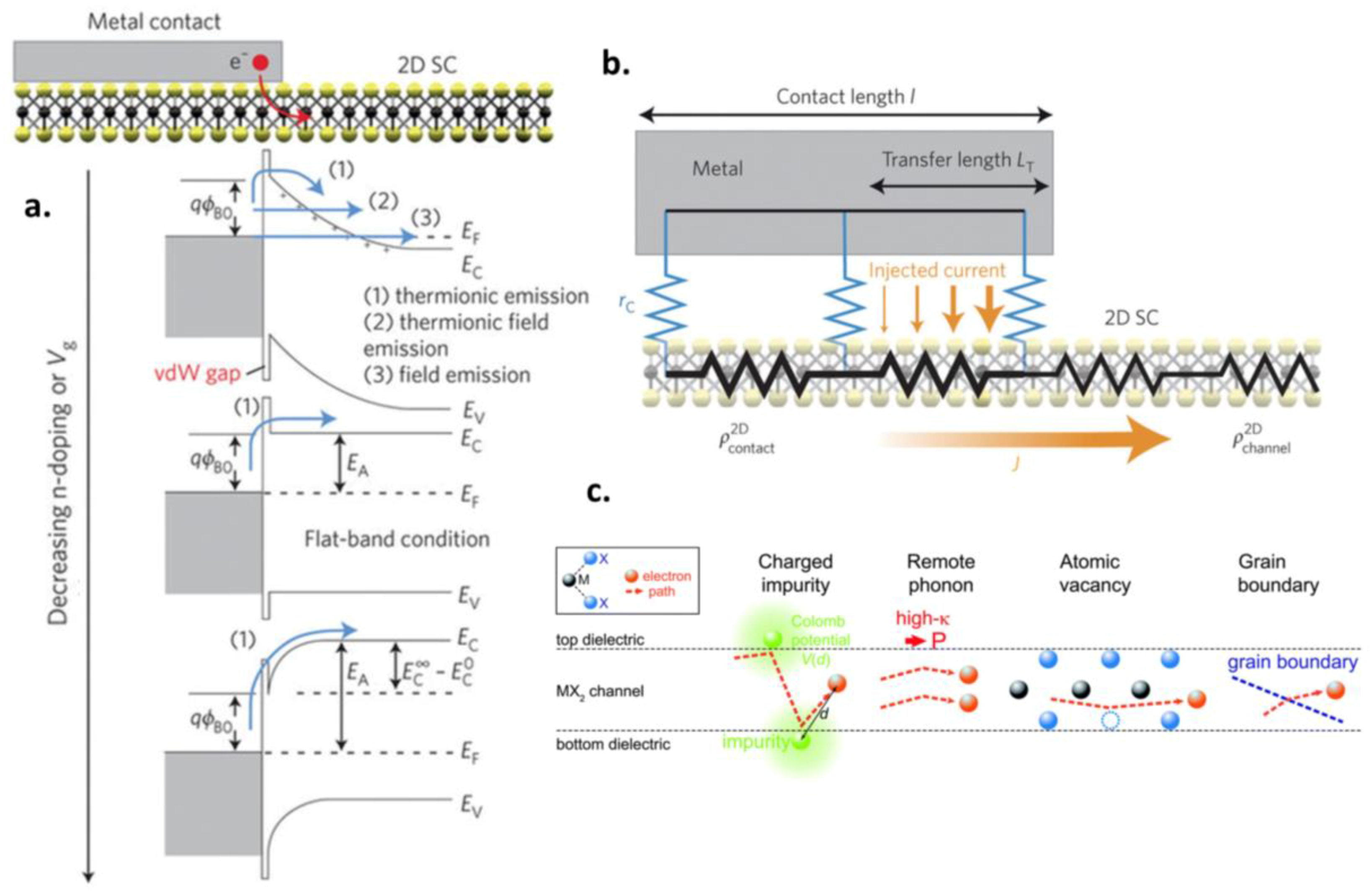
One of the biggest issues confronting MoS2-based devices is the presence of a Schottky barrier (SB) at the interface between MoS2 and the contact metal electrode. This results in a “non-Ohmic” or a Schottky electrical contact characterized by an energy barrier, called the Schottky barrier height (SBH or ΦSB), that hinders the injection of charge carriers into the device channel [132]. Consequently, this notable SBH leads to a large RC and a performance degradation (e.g., low field-effect mobilities) in two-terminal MoS2 devices since a large portion of the applied drain bias gets dropped across this RC [133,134]. The presence of the SBH in MoS2 devices has been experimentally verified by several research groups [134,135,136,137,138,139], and these barriers are thought to be formed due to strong Fermi level pinning (FLP) effects at the contact metal/MoS2 interface [110,132,140]. Detailed microscopic and spectroscopic studies on natural MoS2 flakes revealed high concentrations of defects and impurities, such as sulfur vacancies (SVs) and subsurface metal-like impurities, which are thought to be responsible for the strong FLP [141,142,143,144]. These SV defects/impurities lead to a large background n-doping in the MoS2 and introduce unwanted energy levels or “mid-gap states” closer to the conduction band edge (CBE) within its band-gap that ultimately governs the location of the charge neutrality level where the metal Fermi level gets pinned resulting in fixed barrier heights at the contact/MoS2 interface [145,146,147]. Further insight on the possible origin of this FLP effect was shed by theoretical calculations based on density functional theory (DFT). Kang et al. reported that interactions between certain metals and MoS2 can lead to the formation of a “metal/MoS2 alloy” at the contact interface with a much lower work function than unalloyed MoS2. This leads to an abnormal FLP as if the MoS2 is contacted to a low work function metal [148]. Gong et al., on the other hand, claimed that the FLP mechanism at metal/MoS2 interfaces is unique and distinctively different from traditional metal-semiconductor junctions. According to their calculations, the FLP at the metal/MoS2 interface is a result of two simultaneous effects: first, a modification of the metal work function by interface dipole formation due to the charge redistribution at the interface and, second, by the formation of mid-gap states originating from Mo d-orbitals, that result from the weakening of the intralayer S-Mo bonds due to the interfacial interaction, and the degree thereof, between the metal and the S atom orbitals [149]. A qualitatively similar result was obtained by Farmanbar et al. where they studied the interaction between a wide range of metals and MoS2 using DFT and found that this MoS2/metal interaction leads to the formation of interface states due to perturbation of the MoS2 electronic band-structure, with energies in the MoS2 band-gap that pin the metal Fermi level below its CBE. The extent of this interfacial interaction depends on whether the metal is physisorbed (i.e., weakly adsorbed) or chemisorbed (i.e., strongly adsorbed) on the MoS2 surface, resulting in a small or large density of interface states, respectively. Moreover, the authors showed that by artificially enlarging the physical distance between MoS2 and the metal, these interface states vanished [150]. Experimentally, this physical separation can be achieved by inserting suitable interfacial tunnel barriers or buffer layers in-between the MoS2 and the contact metal (more on interfacial contact tunnel barriers is discussed in Section 8). Additionally, Guo et al. suggested that the strongly pinned SBHs at the metal/2D MoS2 interface arises due to strong bonding between the contact metal atoms and the TMDC chalcogen atoms [151], in accordance with the age-old theory of metal-induced gap states (MIGS) established for metal contacts to conventional bulk 3D semiconductors [152,153,154].
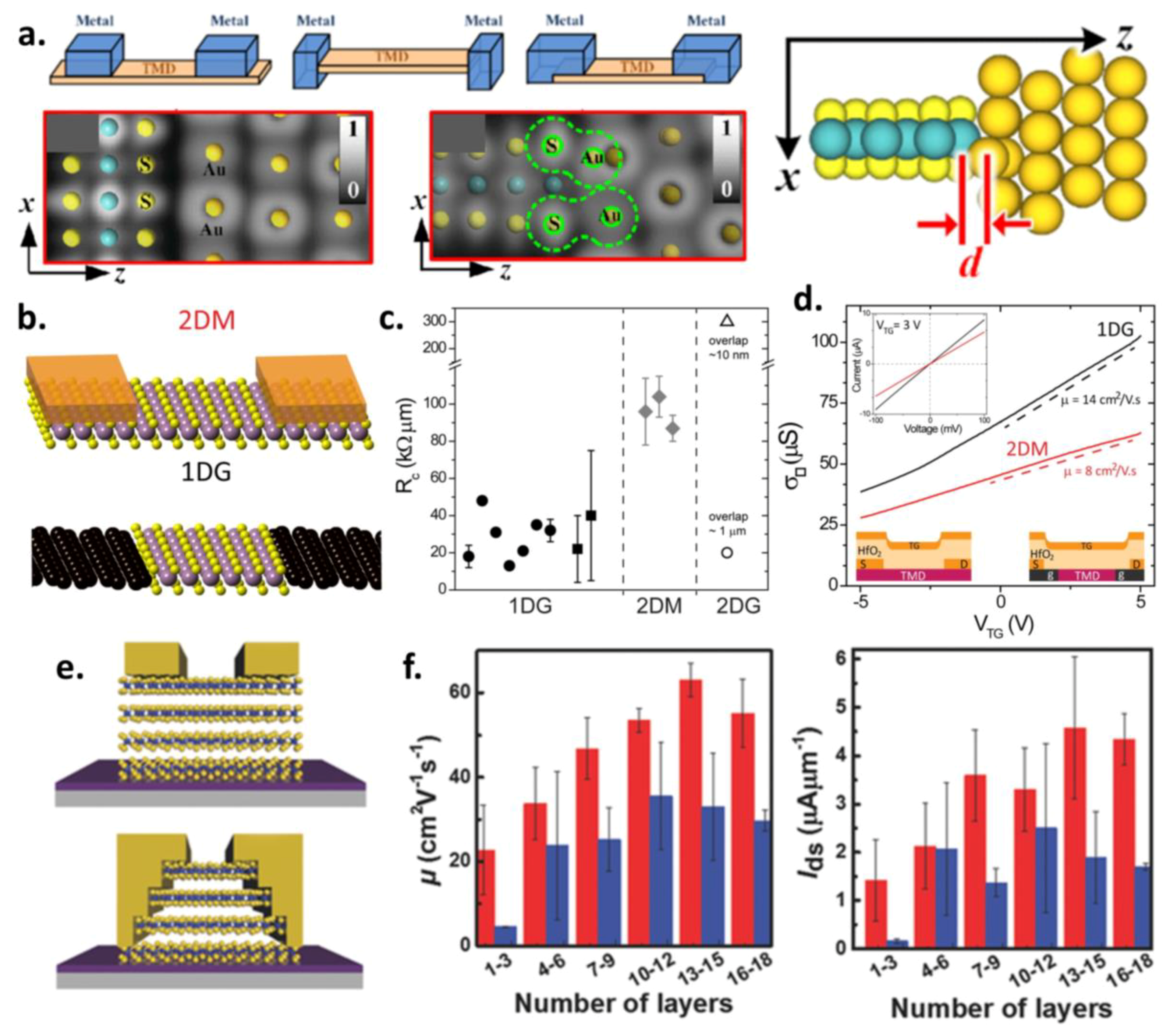
Regardless of the exact underlying physical mechanism involved, FLP is an undesired effect as it leads to fixed SBHs at metal/MoS2 interfaces. It is for this very pinning effect that most metal-contacted MoS2 FETs typically show unipolar n-type behavior as the metal Fermi level gets pinned near the CBE of MoS2 irrespective of the metal work function [135,136,155,156]. In addition to degrading the device performance due to large RC, the reduced tunability of the SBH due to FLP is detrimental towards realizing both n-type and p-type Ohmic contacts to MoS2 desirable for CMOS applications [110]. Besides SBH, another relevant parameter associated with these Schottky barriers is the width of its depletion region in the semiconductor channel or, simply, the Schottky barrier width (SBW). The SBW is largely dependent on the extent of semiconductor “band-bending” in the 2D TMDC/MoS2 channel under the electrode contacted region [157]. Both the SBH and the SBW together determine the charge injection in the 2D MoS2 channel. While SBH governs the extent of thermionic emission of carriers “over” the barrier, SBW determines the extent of thermionic field emission (i.e., thermally-assisted tunneling) and/or field emission (i.e., direct tunneling) “through” the width of this barrier due to the quantum mechanical tunneling of charge carriers (Figure 3a shows the band-alignment at the metal/2D TMDC interface under different gating conditions and illustrates the different charge carrier injection mechanisms) [110,132,158,159]. Hence, both the SBH and SBW must be minimized to achieve efficient injection of charge carriers (electrons or holes) from the contact into the semiconducting MoS2 channel. Additionally, the FLP-induced SBH has been found to depend strongly on the MoS2 layer thickness (especially in the limit of 1–5 layers) since the electronic band-structure of MoS2 undergoes a drastic change as its thickness is decreased (recall that band-gap increases with decreasing MoS2 thickness), leading to a modification of its electron affinity and relative shifts in its band edge positions (i.e., CBE and valence band edge or VBE) in the energy-momentum (or E-k) space [44,160]. Owing to these factors, thinner MoS2 with a larger band-gap typically yields a larger SBH with metal contacts as will be discussed later. This effect is particularly important for devices based on direct band-gap monolayer MoS2 for optoelectronic applications. Finally, in addition to the SB, there are several other important issues that require careful consideration. In an ideal scenario, the surface of TMDCs has an absence or at least a dearth of dangling bonds and, thus, MoS2 does not tend to form interfacial covalent bonds with the as-deposited contact electrodes. Hence, the metal/MoS2 interface is characterized by the presence of a van der Waals (vdW) gap, especially in the top contact geometry (which is most common). This vdW gap acts like an additional “tunnel barrier” for the charge carriers in series with the inherent metal/MoS2 SB (as shown in Figure 3a) and can increase the overall RC [110,134,148]. Moreover, this vdW gap-induced tunnel barrier also manifests itself in multilayer MoS2 devices as additional “interlayer” resistors (since adjacent MoS2 atomic layers are also separated by a vdW gap) and can have implications on the overall device performance. Therefore, for purely electronic applications, the thickness of MoS2 must be carefully chosen for optimum device performance as will be discussed in more detail later. Some elegant ways to overcome this vdW gap issue are to realize “hybridized” top contacts and/or “edge contacts” (that have a greater degree of orbital interaction with the MoS2 atoms/bonds resulting in a more intimate contact having lower RC) instead of the regular top contacts [110,161], and these solutions are discussed in more detail later on along with their promises and inherent challenges.
3.2. Contact Length Scaling, Doping and Extrinsic Carrier Scattering
A major problem arises when we consider “contact length scaling” for MoS2. Contact length (LC) scaling is required when we consider designing aggressively scaled ultra-short-channel devices based on any semiconductor, because LC must be shrunk by a similar factor as the channel length (LCH) as it will determine the final device footprint/density and can lead to chips with smaller area and faster speeds [162,163]. However, while scaling LCH decreases the channel resistance (RCH), scaling LC increases RC in 2D TMDCs. These two effects are contradictory to each other and device performance will ultimately be limited by RC for aggressively scaled devices [164]. LC scaling issue mainly arises from the fact that in 2D TMDCs like MoS2, the transfer length (LT)—i.e., the average length over which the charge carriers move in the semiconductor before being transferred to the contact electrode (also referred to as the “current crowding” effect at metal/semiconductor contacts) [165,166,167]—is often large (Figure 3b shows the schematic illustration of this current crowding effect at the metal/2D TMDC junction using a resistor network model). For example, LT = 600 nm for monolayer MoS2 [157] and 200 nm for six-layer MoS2 with Ti contacts [167]. If the LC is scaled below LT (i.e., LC << LT), then RC increases as per the relation RC = ρC/LC where ρC is the specific contact resistivity [note that RC is independent of LC when LC >> LT and is then given by the relation RC = √(ρC ρSH) where ρSH is the sheet resistance of the semiconducting channel underneath the contact] [110,168]. Therefore, for ultra-short-channel FETs (targeting the sub-10 nm node) based on 2D MoS2, it is extremely important to minimize ρC or, in other words, minimize LT [since LT = √(ρC/ρSH)] to achieve low RC. This is important because the RC of any FET must only be a small fraction (~20%) of the total FET resistance (i.e., RCH + 2RC) for the transistor to operate properly while ensuring that its current-voltage (I-V) behavior is primarily determined by the intrinsic channel resistance RCH [110,112]. Hence, it is imperative that RC must scale (i.e., reduce) together with both LCH and LC before MoS2-based FETs can come anywhere close to rivaling the performance of state-of-the-art Si and III-V device analogs (for reference, the RC values reported for most TMDC/MoS2 FETs to date are about an order of magnitude higher than in today’s Si Fin-FET technologies where RC is well below 100 Ω·µm) [110,111,132]. Now, the ρC is strongly dependent on the SBH among other factors, hence minimizing or eliminating the SBH is a guaranteed way to alleviate the RC issue in MoS2 FETs. Next, the ultra-thin nature of the 2D MoS2 makes it incredibly challenging to employ conventional CMOS-compatible doping techniques (ion implantation or high-temperature diffusion) to perform controlled and area-selective doping to control the carrier type (n or p) and carrier concentration (ranging from degenerate in the source/drain contact regions to non-degenerate in the channel region) in MoS2 FETs, especially at the monolayer limit [169]. This is primarily because the atomically thin MoS2 lattice is highly susceptible to structural damage and etching which, for example, is typically unavoidable in the ion implantation process [170]. Lastly, MoS2 devices typically show much lower intrinsic carrier mobilities in experiments than the predicted phonon-limited values, implying the existence of extrinsic carrier scattering sources. Thus, it is important to eliminate or minimize the effect of these extrinsic charge carrier scattering mechanisms, such as substrate remote phonons, surface roughness, charged impurities, intrinsic structural defects (e.g., SVs), interface charge traps (Dit) and grain boundary (GB) defects (Figure 3c schematically illustrates some prominent extrinsic charge carrier scattering mechanisms), that can severely degrade the mobility in MoS2-based devices [160,171,172,173,174,175,176,177,178,179].
3.3. Tackling the Major Challenges
To achieve low-power, high-performance and ultra-scaled devices based on 2D MoS2, it is highly necessary to come up with effective solutions to alleviate the various problems, as mentioned above, that have an adverse effect on key device performance metrics. It is worth noting that solutions to several of these problems are intertwined and solving one can alleviate the other. As an obvious case, reduction of the SB (either by minimization of the SBH or thinning of the SBW) lowers the RC and effectively improves the charge injection efficiency and the field-effect mobility (µFE) of the MoS2 FETs. Reduction of the SBH can lead to a reduced specific contact resistivity ρC. With area-selective and controlled doping, one can potentially realize degenerately doped S/D contact regions in MoS2, just like in the conventional Si-CMOS case, to achieve Ohmic contacts. Realization of edge contact to few- or multilayer MoS2, such that each individual layer of the stack is independently contacted, can not only help in eliminating the vdW gap-induced tunnel barriers, it can also be useful in terms of contact scaling and overall device area/footprint reduction. Unsurprisingly, therefore, there has been an extensive research effort in the past few years to explore effective solutions for mitigating the challenges associated with the contact, doping and mobility engineering of 2D MoS2 devices. These solutions are categorically discussed in the various sections below, highlighting several insightful experimental and theoretical results reported thus far. The reader should note that, although the discussion is focused on MoS2, majority of these issues, along with their underlying concepts and engineering solutions, are readily applicable to other members of the semiconducting 2D TMDC family (e.g., MoSe2, WS2, and WSe2) as well.
4. Contact Work Function Engineering
A very straightforward approach to minimize the SBH for either electrons or holes has been through “work function” (ΦM) engineering of the contact electrodes. In an ideal scenario, without any FLP, Fermi level of low ΦM contacts (typically ΦM < 4.5 eV) can align closer to the CBE of MoS2 (since the electron affinity of MoS2 is about 4.2 eV) resulting in smaller SBH for electrons and, likewise, the Fermi level of large ΦM contacts (typically ΦM > 5 eV) can align closer to the VBE of MoS2 resulting in smaller SBH for hole injection. This is known as the Schottky–Mott rule or the Schottky limit, wherein the SBH at any metal/semiconductor junction can be determined by the difference between the metal’s work function and the semiconductor’s electron affinity [110,158,180]. One would assume then, that by choice of a proper metal work function, it would be possible to eliminate the SBH and realize purely Ohmic contacts. In reality, however, hardly any metal/semiconductor (MS) junctions (including those for traditional bulk or 3D semiconductors) follow this rule due to the FLP effect, and the Fermi level at the MS interface is typically pinned at the interface state energy (referred to as the Bardeen limit of pinning) arising due to MIGS [152,153,154,181,182]. Hence, the contact Fermi level lies somewhere in-between the Schottky limit (i.e., no pinning) and the Bardeen limit (i.e., perfect pinning) depending on the severity of the FLP, which ultimately determines the SBH [180]. Strategies to achieve Fermi level “depinning” can, therefore, be important to realize true Ohmic contacts by virtue of contact work function engineering alone (as will be discussed later). However, even in the presence of strong FLP effect, as observed in 2D MoS2 (due to reasons described before), and despite the fact that metals typically get pinned near the CBE of MoS2 resulting in the largely observed n-type device behavior, it has been shown that the magnitude of the SBH at the contact/MoS2 interface can be directly correlated to the work function of the contact metal. Efforts to achieve p-type injection in MoS2 via work function engineering are also discussed.
4.1. N-Type Work Function Engineering
For n-type few-layer MoS2 devices, Das et al. showed that low work function metals such as scandium (Sc, ΦM = 3.5 eV) and titanium (Ti, ΦM = 4.3 eV) yield a lower SBH for electron injection into the MoS2 conduction band, resulting in a lower RC, than higher work function metals such as nickel (Ni, ΦM = 5.0 eV) and platinum (Pt, ΦM = 5.9 eV) [135]. From a detailed temperature-dependent study that accounted for both thermionic emission over the SBH and thermally-assisted tunneling through the SBW, the authors extracted the true SBH (i.e., ΦSB extracted at the flatband voltage) to be ~30 meV, ~50 meV, ~150 meV, and ~230 meV for Sc, Ti, Ni, and Pt, respectively, clearly suggestive of the strong FLP near the CBE of MoS2 (the Fermi level pinning factor S = dΦSB/dΦM was around 0.1 indicative of strong pinning). Moreover, the extracted field effect mobilities were found to be 21, 90, 125, and 184 cm2/V-s for Pt, Ni, Ti, and Sc contacts, respectively, clearly highlighting the detrimental effect of large SBHs on both the RC and the ON-state device performance (Figure 4a,b show the expected and true metal Fermi level line-up with the MoS2 electronic bands, respectively, with Sc providing the best electron injection) [135]. Similar to the case of Sc contacts, Liu et al. showed that low work function Ti could also be used as an efficient n-type contact for few-layer (5–15 layers) MoS2. Using Ti, they achieved a low RC of 0.8 kΩ·µm and, based on theoretical calculations, surmised that Ti can heavily dope the MoS2 surface leading to a good contact. Moreover, the authors emphasized upon the importance of MoS2 layer thickness, post-contact “annealing” and realizing “edge contacts” to enhance the performance of few-layer MoS2 devices with Ti contacts [183]. In particular, edge contacts to few- or multilayer devices are more promising because each individual layer in the few-layer device can be independently contacted from the side (more on the effects of MoS2 layer thickness on the SBH and carrier mobility is discussed in Section 10, while Section 11 discusses the advantages of making side or “edge contacts” to few- or multilayer MoS2).
In another work, Hong et al. combined thin layers of low work function aluminum (Al, ΦM = 4.06–4.26 eV) sandwiched in-between MoS2 and indium zinc oxide (IZO), a transparent conducting oxide having a large work function (ΦM ~5.14 eV), to realize high-performance and transparent multilayer MoS2 FETs. The low work function Al contact led to a much reduced SBH resulting in a 24-fold increase of the field-effect mobility (from 1.4 cm2/V-s in MoS2/IZO to 33.6 cm2/V-s in MoS2/Al/IZO), three orders of magnitude enhancement in the ON/OFF current ratio, robust current saturation and linear output characteristics in these MoS2 FETs (Figure 4c explains the SBH lowering due to the insertion of low ΦM Al in-between IZO and MoS2 via band diagrams). Moreover, the transparent IZO S/D electrodes allowed a transmittance of 87.4% in the visible spectrum [184]. Recently, in a major push towards large-area fully transparent MoS2 electronics, Dai et al. demonstrated aluminum-doped zinc oxide (AZO) transparent contacts deposited via atomic layer deposition (ALD), with tunable conductivity and work function, to make Ohmic contacts to CVD-grown MoS2. The work function and resistivity of the AZO film could be tuned by changing the Zn:Al subcycle ratio during the ALD growth process and optimized AZO films with a combination of low resistivity and low work function (ΦM ~4.54 eV, similar to Ti) were chosen as contacts. Overall, the AZO-contacted CVD MoS2 FETs showed promising performance with linear output characteristics at RT (suggesting Ohmic-like contacts), a µFE of 4.2 cm2/V-s, low threshold voltage (Vth) of 0.69 V, low SS of 114 mV/decade, large ON/OFF ratio >108, and an average visible-range transmittance of 85% for fully transparent MoS2 FETs on glass substrates (with AZO S/D and gate contacts, and HfO2 gate dielectric) [185]. To achieve more effective n-type work function engineered contacts, mitigating the deleterious effects of strong FLP at the 3D metal/2D semiconductor interface, Liu et al. suggested the use of surface engineered 2D “MXenes” as a potential SB-free n-type metal contact to MoS2. 2D MXenes are a class of metal carbides/nitrides with the general formula Mn+1XnTx (where M is an early transition metal, X is C and/or N, T represents a surface terminating group, and n = 1–3) that can make a vdW contact to MoS2 having an inherent vdW gap. This weak vdW interaction can suppress the formation of gap states at the interface leading to a weaker FLP than conventional 3D metal contacts. Moreover, based on first principles calculations, the authors showed that MXenes having “OH” as the surface terminating group can have very low work functions (<3 eV) due to surface dipole effects, even lower than that of Sc metal, leading to Ohmic contacts [186].
4.2. P-Type Work Function Engineering
For realizing p-type MoS2 devices, Chuang et al. used substoichiometric molybdenum trioxide (MoOx, x < 3), an extreme high work function transition metal oxide with ΦM = 6.6 eV, in the S/D contacts and demonstrated efficient hole injection in the MoS2 valence band, as opposed to high work function metals that typically showed n-type behavior due to strong FLP. The efficacy of MoOX as a hole injector was attributed not only to its high ΦM, but also to its better interface properties (such as lower tendency to form MIGS than elemental metals) that caused a lower degree of FLP. Using MoOx, the authors could demonstrate MoS2 PFETs (essential for realizing CMOS-type devices together with MoS2 NFETs) with ON/OFF ratios ~104, and MoS2 Schottky diodes with asymmetric MoOx and Ni contacts. The SBH for holes was extracted to be ~310 meV for MoOx/MoS2 contacts (Figure 4d,e show the FET schematic as well as the qualitative band diagrams, and the p-type transfer curves for the MoOx-contacted MoS2 FETs, respectively) [187]. A detailed theoretical investigation by McDonnell et al. further revealed that the work function of MoOx should be sufficient to provide an Ohmic hole contact to MoS2 (provided carbon impurities and Mo5+ concentration at the interface can be carefully controlled) [188]. Like high work function MoOx, high work function graphene oxide (GO, ΦM ~5–6 eV) has also been proposed as an efficient hole injector in monolayer MoS2. Theoretically, the p-type SBH at the MoS2/GO interface can be made smaller by increasing the oxygen concentration and the fraction of epoxy functional groups in GO (which increases its ΦM). Compared to MoOx, GO can be promising as it is easier to fabricate, and its production methods are simpler and inexpensive [189].
More recently, an extremely promising experimental approach to realize low-resistance p-type Ohmic contacts to MoS2 FETs was demonstrated by Chuang et al. where they utilized a “2D/2D” vertical heterostructure contact strategy [190]. In their approach, the undoped semiconducting MoS2 channel is contacted in the S/D regions by degenerately p-doped Mo0.995Nb0.005S2 [the degenerately p-doped MoS2 was obtained by substitutional doping of MoS2 using niobium (Nb) during the crystal growth process; more on substitutional doping of MoS2 is discussed in Section 15]. The work function difference between the undoped and the degenerately p-doped MoS2 creates a band offset across the 2D/2D vdW interface. This band offset can be electrostatically tuned by a back gate voltage owing to the weak interlayer vdW interaction at the 2D/2D junction, essentially resulting in a negligible SBH in the ON-state of the FET (Figure 4f illustrates the working principle of MoS2 PFETs with 2D/2D contacts via band diagrams). Note that the vdW interface also promotes weaker FLP by suppressing the formation of interface gap states. The authors reported field-effect hole mobilities as high as 180 cm2/V-s at RT, observation of a metal-insulator transition (MIT) in the temperature-dependent conductivity, and linear output characteristics down to 5 K in their p-type MoS2 FETs with these low-resistance 2D/2D contacts [190]. Finally, an alloyed 2D metal/MoS2 contact scheme, similar to recent reports on 2D tungsten diselenide (WSe2) where a NbSe2/WxNb1−xSe2/WSe2 contact interface was realized (here NbSe2 is a metallic 2D TMDC), could also be used to facilitate p-type MoS2 FETs. Such alloyed 2D junctions have been shown to have atomically sharp vdW interfaces with both reduced interface traps and SBH, and can help maximize the electrical reliability of 2D devices [191]. In the same context of 2D/2D vdW contacts, and as described in the previous section for n-type contacts, Liu et al. also predicted that 2D MXenes with “O” surface terminations can yield a p-type SB-free contact to MoS2, as some of the O-terminated MXenes can have a rather high work function that is even higher than that of elemental Pt [186]. Additionally, in a separate theoretical study, Liu et al. predicted that 2D niobium disulfide (NbS2), a 2D TMDC metal with a high work function (>6 eV), can be a promising 2D electrode for achieving low SBH for p-type contacts to MoS2 while combining all the advantages associated with a vdW interface and weak FLP [140].
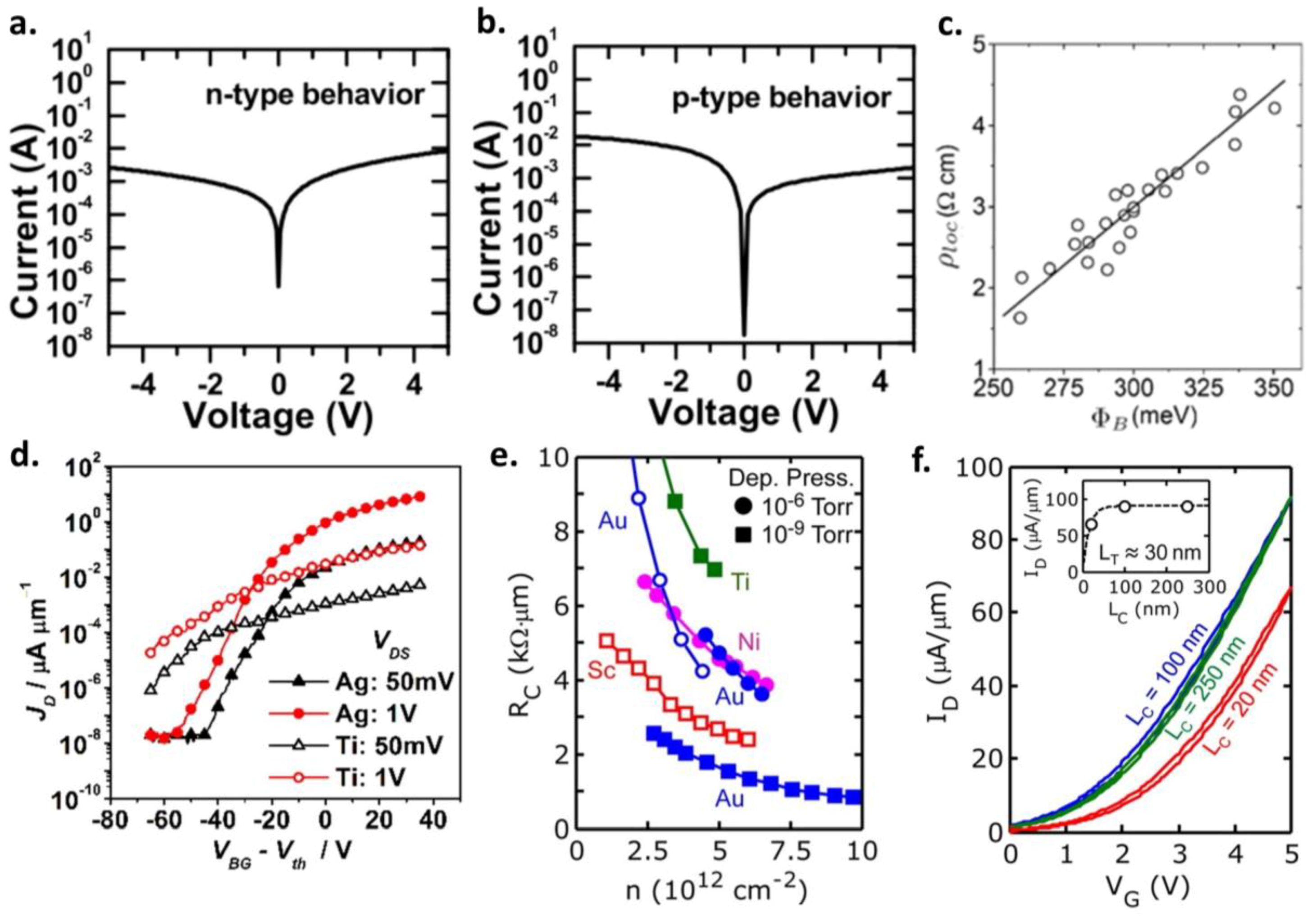
5. Effect of Stoichiometry, Contact Morphology and Deposition Conditions
While work function engineering of the contacts seems a simple and straightforward approach to realize either n- or p-type contacts with low SBHs to MoS2 (taking FLP into account of course), there are other reports that reveal that contact work function engineering alone is not always a good predictor for forming high-quality electrical contacts to MoS2. For instance, McDonnell et al., in their study of structural defects on MoS2, found that both n- and p-type regions can exist at different sites on the same MoS2 sample. The n-type regions were found to be S-deficient (S/Mo ratio ~1.8:1), whereas the S/Mo stoichiometry in the p-type regions was 2.3:1, indicating that these regions were either S-rich or Mo-deficient. These variations in the structural defect density can strongly impact the observed n- or p-type I-V characteristics in MoS2 devices irrespective of the contact metal (Figure 5a,b show both n- and p-type behavior, respectively, with the same Au contacts at different MoS2 locations) [141]. This nanoscale spatial inhomogeneity on the MoS2 surface was further elucidated by Giannazzo et al. where they used high resolution conductive atomic force microscopy (CAFM) to study the spatial variations in the SBH (ΦSB) and local resistivity (ρloc). They found an excellent correlation between the ΦSB and ρloc values, with low (high) ρloc regions corresponding to low (high) ΦSB regions (see Figure 5c), and concluded that the low resistivity/low SBH regions were a result of n-type SV clusters on the MoS2 surface [192]. Yuan et al. highlighted the importance of metal/MoS2 interface morphology, and the thermal conductivity of the metal, on the performance of MoS2 FETs. They compared monolayer and few-layer MoS2 devices with Ag and Ti contacts, both having a similar low work function (ΦM = 4.3 eV) and showed that devices with Ag contacts had 60× larger ON-state currents than those with Ti contacts. This was attributed to the significantly smoother and denser topography of Ag films on MoS2 owing to the excellent wettability of Ag on MoS2 as well as to the higher thermal conductivity of Ag (~20× larger than Ti) that can enhance the heat dissipation efficiency and, hence, prevent heat-induced mobility degradation in MoS2 FETs (Figure 5d shows a comparison of the transfer characteristics between identical MoS2 FETs with Ag and Ti contacts) [193].
The excellent wettability and morphology of Ag on MoS2 was further exploited by Kim et al. to demonstrate, for the first time, low-cost inkjet-printed Ag S/D electrodes on large-area CVD-grown monolayer MoS2 FETs, using a commercial nanoparticle-type Ag ink and a drop-on-demand printer. The favorable surface interaction between Ag and MoS2 makes Ag-based printable inks highly compatible for enabling inkjet-printed electrodes on MoS2, a process that is promising for large-area and low-cost MoS2-based thin-film electronics [194]. English et al. revealed the importance of metal deposition conditions and showed that gold (Au), a high work function metal (ΦM = 5.1 eV), deposited under ultra-high vacuum (UHV) conditions (base pressure ~10−9 Torr) yielded a cleaner, higher quality and air-stable (over 4 months) metal/MoS2 contact with a low RC of ~740 Ω∙µm, that was even lower than the RC achieved using low ΦM metals, such as Sc, Ti and Ni, on MoS2 (Figure 5e compares RC versus n2D for various metals deposited on MoS2 under two different deposition base pressures) [164,195]. The authors also studied the effects of MoS2 FET scaling and found that the RC starts dominating the overall device performance below LCH = 90 nm. Moreover, the effects of LC scaling were also analyzed and, as expected, a current degradation of 30% was observed when LC became less than LT due to increase in the RC when LC << LT, as explained earlier in Section 3.2 (Figure 5f shows the transfer characteristics of MoS2 FETs evaluated at varying contact lengths LC) [164]. The importance of base vacuum pressure while depositing contacts (especially low ΦM reactive metals) on MoS2 was also highlighted by McDonnell et al. where they studied Ti contacts deposited under high vacuum (HV, ~10−6 mbar) and UHV (~10−9 mbar) using X-ray photoelectron spectroscopy (XPS). Under HV, an interfacial TiO2 layer is formed due to the oxidation of Ti, whereas metallic Ti is deposited under UHV that can react with the MoS2 to form less conductive TixSy and metallic Mo at the interface [196]. Similarly, Smyth et al. performed an intensive XPS study to reveal the interfacial chemistry between high work function (Au and Ir) and low work function (Cr and Sc) metals deposited on MoS2 under HV and UHV deposition ambient. They found that while Au does not react with MoS2 regardless of the reactor ambient, Ir leads to interfacial reactions with MoS2 under both HV and UHV. In contrast, both Cr and Sc lead to interfacial reactions under UHV. Additionally, Sc is rapidly oxidized, whereas Cr is only partially oxidized when deposited under HV conditions [197]. Thus, it is evident that the deposition chamber ambient or base pressure can strongly influence the contact/MoS2 interface chemistry and, ultimately, the SB and RC in MoS2 devices.
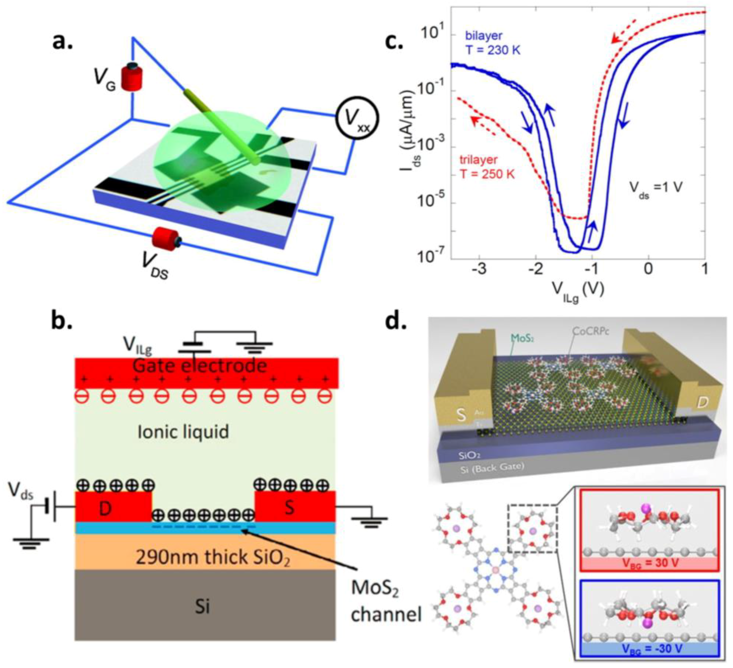
6. Electric Double Layer (EDL) Gating
Several groups have also demonstrated the concept of electric double layer (EDL) gating on 2D MoS2 devices using a variety of liquid, solid and gel-based “electrolytes” that serve as the gating medium. In a typical EDL gating approach, an ionic liquid (IL) or a solid polymer electrolyte (PE) is drop-casted on top of an MoS2 FET (typically back-gated) covering the entire FET area along with its S/D contacts. The electrolyte is electrostatically gate-controlled through a top electrode or a side electrode pre-fabricated near the device channel (Figure 6a shows the schematic illustration of the EDL gating approach on MoS2 FETs). When a positive (negative) voltage is applied on the gate electrode, mobile negative (positive) ions in the electrolytic medium accumulate near the gate electrode, whereas positive (negative) ions accumulate near the MoS2 channel, leading to the formation of an EDL at the interfaces between the IL/PE electrolyte and solid surfaces (i.e., the gate electrode and the MoS2 surface). At the MoS2 interface, this results in the induction of either electrons or holes in the channel (depending on the gate bias polarity) essentially doping the channel either n- or p-type (Figure 6b schematically illustrates the formation of the EDL at the electrolyte/solid interfaces) [120,198,199,200,201,202,203]. A major advantage of the EDL gating/doping technique is that extremely high sheet carrier densities (on the order of n2D ~1014 cm−2; much higher than the carrier densities achievable in MoS2 FETs gated using solid dielectrics, e.g., SiO2 or high-κ dielectrics) along with broad carrier density tunability can be realized in the channel due to the large geometrical capacitances and highly efficient gating afforded by the thin EDL layer. Moreover, the doping-induced high carrier densities cause a large band-bending in the MoS2 channel which is beneficial for minimizing the RC at the MoS2/contact interface due to substantial reduction of the Schottky-depletion width (or the SBW) allowing for easy injection of carriers in the channel via tunneling. This results in increased FET carrier mobilities (µFE). Although the EDL technique is promising for investigating the electronic transport properties of MoS2, it has some major drawbacks which make it unsuitable for practical device applications. For example, the ionic liquids are unstable, sensitive to moisture, and chemically reactive. Hence, the device measurements must be carried out under high vacuum and at low-temperatures. Moreover, both the liquid and solid electrolytes are physically bulky (several microns thick) and cannot be scaled to nanoscale dimensions [120,198,199,200,201,202,203].
Despite these limitations, the use of EDL gating on MoS2 has shown some interesting device behavior. The first report of EDL gating using an ionic liquid on MoS2 was by Zhang et al. where they demonstrated ambipolar operation in thin MoS2 flakes characterized by large ON-state conductivities and ON/OFF ratios >102 for both the electron and hole branches. The n2D reached 1.0 and 0.75 × 1014 cm−2 for electrons and holes at |VG| = 3 V, respectively, while their maximum Hall mobilities were 44 and 86 cm2/V-s, respectively [198]. Perera et al. reported ambipolarity, significantly higher electron mobilities (~60 cm2/V-s at 250 K) and near ideal SS (~50 mV/decade at 250 K) in ionic liquid gated MoS2 FETs as compared to comparable back-gated MoS2 FETs (Figure 6c shows the ambipolar behavior in the transfer characteristics of the IL-gated MoS2 FET). They observed an increase in the electron mobility from ~100 to 220 cm2/V-s as the temperature was lowered from 180 K to 77 K. This performance enhancement was primarily attributed to the reduction of the SB at the S/D contact interface by the enhanced MoS2 band-bending due to EDL doping [200]. The use of a solid PE as an EDL gate on monolayer MoS2 was shown by Lin et al. where they used a PE consisting of poly(ethylene oxide) (PEO) and lithium perchlorate (LiClO4) as a SB reducer and a channel mobility booster. In this case, the PEO serves at the polymer base, whereas the Li+ and ClO4− ions serve as the mobile ionic dopants. A three order of magnitude enhancement in the electron mobility (from 0.1 to 150 cm2/V-s) was achieved that was attributed to the reduction of the contact SB as well as to an “ionic screening” effect. Moreover, PE-gated devices showed a near ideal SS (~60 mV/decade at RT, implying high gating efficiency) and high ON/OFF ratios (~106) [199]. A similar PE gating approach, using PEO polymer medium and cesium perchlorate (CsClO4) as the ion source (Cs+ and ClO4−), was used by Fathipour et al. which yielded an RC of 200 Ω·µm (comparable to the best RC reports on MoS2) and high current densities (~300 µA/µm) in MoS2 NFETs [204]. Recently, a “2D electrolyte” capable of electrostatically doping the surface of MoS2 was introduced by Liang et al. The electrolyte is only 0.5–0.7 nm thick and consists of an atomically thin cobalt crown ether phthalocyanine (CoCrPc) and LiClO4 molecules, such that one CoCrPc molecule can solvate one Li+ ion. In this technique, the CoCrPc is deposited on the 2D MoS2 surface by drop-casting and annealing to form an ordered array. The Li+ ion location with respect to the CoCrPc/MoS2 interface can be modulated by a gate bias, similar to the conventional EDL approach, to dope the MoS2 by inducing image charges on the MoS2 surface, with n2D as high as ~1012 cm−2 (Figure 6d schematically illustrates the concept of 2D CoCrPc-based electrolytes and the relative movement of the Li+ ion with respect to the CoCrPc/MoS2 interface). Moreover, the 2D electrolyte shows “bistability”, with the extent of n-doping (either more or less) dependent on the magnitude and polarity of the external gate bias [205]. This work is indeed promising as it shows that electrolytes can be scaled to atomically thin dimensions and can be used for adjustable doping/gating of 2D MoS2, but the ambient stability of the 2D electrolyte is still under scrutiny.
7. Surface Charge Transfer Doping
Surface charge transfer doping, utilizing various chemical/molecular reagents and sub-stoichiometric high-κ oxides, has been investigated as an alternative method to achieve controllable channel doping as well as access region doping to alleviate the SB/RC issue in MoS2 FETs. In this approach, depending on the electron affinity/work function of the adsorbed or deposited interfacial specie, electrons either get donated to or accepted from the MoS2 surface resulting in n-type or p-type doping, respectively. This technique typically involves heavily doping the contact/access regions of the MoS2 FET with electrons/holes which renders the SB transparent due to substantial “thinning” of the SBW (due to large band-bending in the highly doped MoS2 near or underneath the contact). Thus, the charge carriers can easily “tunnel” through the narrow SBW into the channel resulting in Ohmic contacts. Conceptually, this approach is similar to that used in conventional Si CMOS technology where the S/D regions are degenerately doped by donor (e.g., P and As) or acceptor (e.g., B) species to facilitate carrier tunneling and low RC for n- and p-type contacts, respectively, at the metal-semiconductor contact interface [206,207,208].
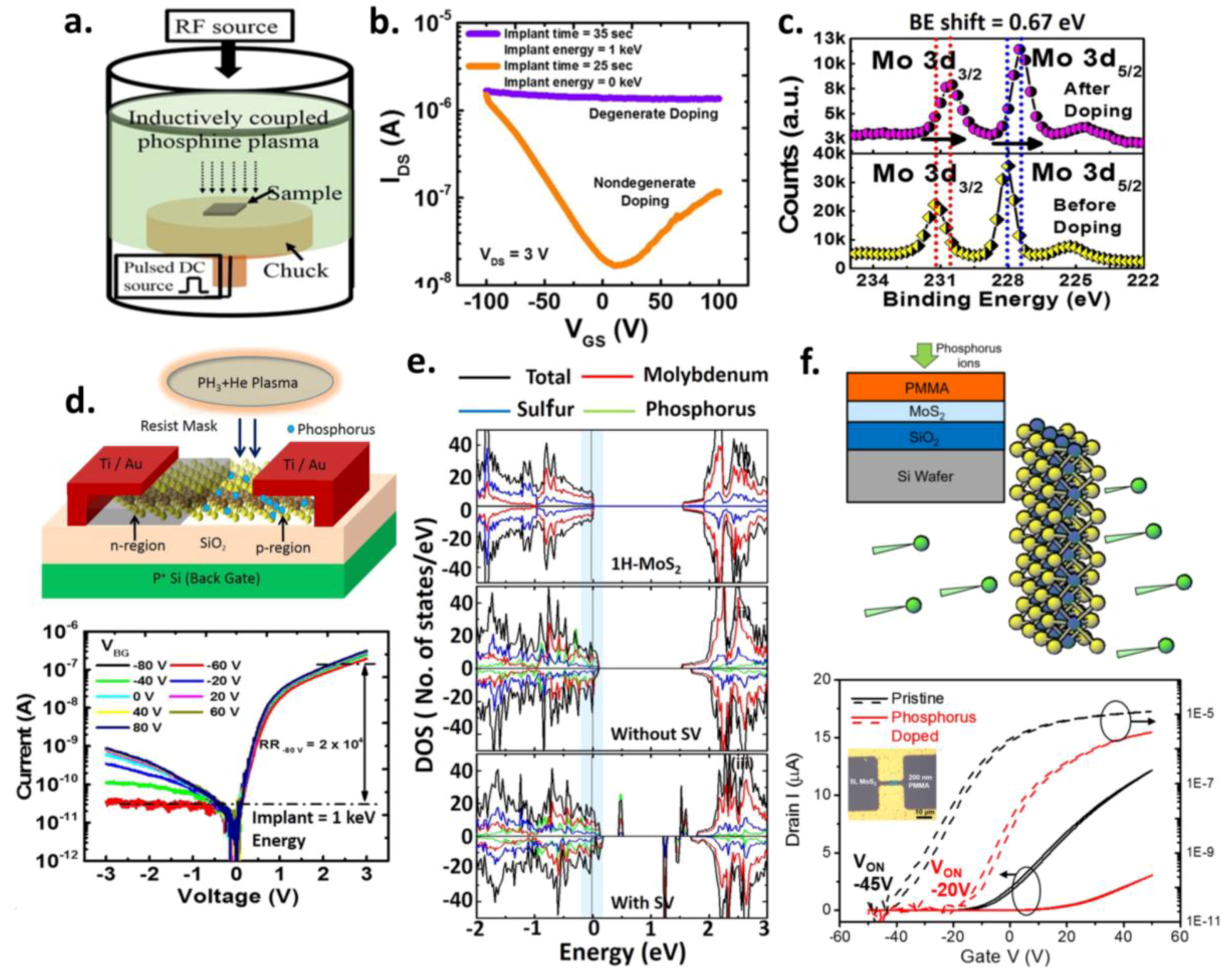
7.1. Charge Transfer Electron Doping
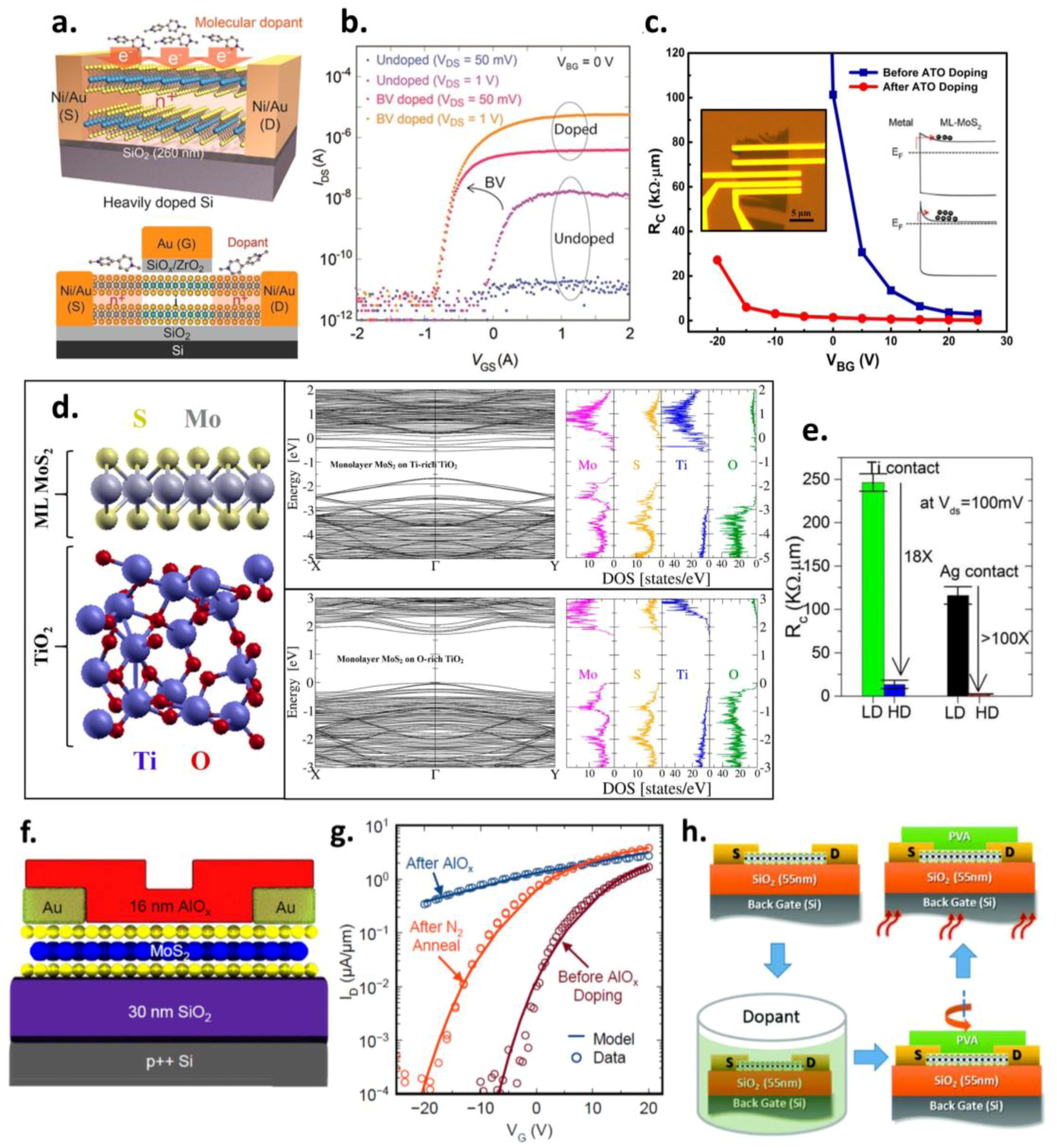
Initial studies on MoS2 devices utilized strong electron-donating reactive chemical species such as polyethyleneimine (PEI) [209] and reactive group-I metals such as potassium (K) [210]. Although successful electron doping, and an improvement in the MoS2 FET performance (by reduction of the sheet/contact/access resistances), was achieved using these techniques, the doping reagents used were unstable under ambient conditions and, hence, practically unfeasible [209,210]. The first air- and vacuum-stable n-type charge transfer doping of MoS2 was subsequently demonstrated by Kiriya et al. using benzyl viologen (BV), an electron donor organic compound having one of the highest reduction potentials. Using BV doping, the authors obtained an electron sheet density of ~1.2 × 1013 cm−2, which corresponds to the degenerate limit for MoS2 as well as a 3× reduction in the RC of MoS2 FETs (Figure 7a,b show the schematic illustration of the BV doping process, and performance enhancement in the transfer curves of the MoS2 FET after BV doping, respectively). Moreover, the BV dopant molecules could be reversibly removed by immersion in toluene, thereby promoting controlled and selective-area doping [211]. In an interesting experimental and theoretical study, Rai et al. demonstrated the use of sub-stoichiometric high-κ oxides, such as TiOx (x < 2), HfOx (x < 2) and Al2Ox (x < 3), as air-stable n-type charge transfer dopants on monolayer MoS2. This high-κ oxide doping effect, arising due to interfacial-oxygen-vacancies in the high-κ oxide, could be used as an effective way to fabricate high-κ-encapsulated top-gated MoS2 FETs with selective doping of the S/D access regions to alleviate the RC issue, merely by adjusting the interfacial high-κ oxide stoichiometry (Figure 7c shows the RC of a back-gated monolayer MoS2 FET, extracted using the transfer length measurement or “TLM” method, as a function of back gate bias before and after sub-stoichiometric TiOx doping) [212,213]. The underlying doping mechanism is similar for all high-κ oxides and involves the creation of donor states/bands near the CBE of MoS2 by the uncompensated interfacial metal atoms of the sub-stoichiometric high-κ oxides. Moreover, this doping effect is absent in the case of purely stoichiometric high-κ oxides as has been verified both experimentally as well as theoretically using DFT calculations [212,213,214] (Figure 7d compares the DFT band-structures and atom-projected-density-of-states, AP-DOS, for both an oxygen-rich, i.e., stoichiometric, and an oxygen-deficient TiOx/MoS2 interface confirming the n-doping effect only in the latter case). Using this doping technique, the authors reported an RC as low as 180 Ω·µm in TiOx-encapsulated monolayer MoS2, that is among the lowest reported RC values for monolayer MoS2 FETs. The extracted transfer length LT reduced from 145 nm before doping to 15 nm after TiOx doping highlighting the effectiveness of heavily doping the MoS2 near the contact regions to drive down the LT which is important for ultra-scaled devices. Moreover, an enhancement in both the µFE and intrinsic mobility was observed, strongly indicating that this high-κ doping effect plays an important role in boosting the electron mobility in high-κ-encapsulated MoS2 FETs.
In similar reports, both McClellan et al. and Alharbi et al. demonstrated the efficacy of n-doping by sub-stoichiometric high-κ oxides in improving the performance of MoS2 FETs. Alharbi et al. used sub-stoichiometric HfOx as the top gate dielectric in FETs fabricated on CVD-grown monolayer MoS2 and achieved an RC as low as ~480 Ω·µm under heavy HfOx doping (>100× improvement than the light HfOx doping case) and a mobility of ~64 cm2/V-s (Figure 7e shows the improvement in RC for both Ti- and Ag-contacted top-gated MoS2 FETs under light and heavy HfOx doping). Moreover, the top-gated geometry allowed effective control over the channel resulting in an SS of ~125 mV/decade and an ON/OFF ratio > 106 [215]. McClellan et al., on the other hand, utilized AlOx encapsulation to n-dope back-gated monolayer MoS2 FETs and achieved an RC of ~480 Ω·µm, a µFE of ~34 cm2/V-s and a record ON-current of 700 µA/µm. A key step in their approach was annealing of the MoS2 devices in an N2 ambient after AlOx encapsulation, which helped restore the SS and µFE by converting the “deep-level traps” at or near the AlOx/MoS2 interface into “shallow-level donors” (Figure 7f,g show the back-gated MoS2 FET schematic, and the effect of AlOx doping, as well as N2 post-annealing on the FET transfer curves, respectively) [216]. Besides n-doping using sub-stochiometric high-κ oxide encapsulation, poly(vinyl-alcohol) (PVA) polymeric coatings can also be used as strong n-type dopants for MoS2 as shown by Rosa et al. They showed a 30% reduction in the RC and the sheet resistance (RSH) was reduced from 161 kΩ sq−1 to 20 kΩ sq−1 after PVA doping (Figure 7h schematically illustrates the PVA coating process). The non-covalent and non-destructive PVA doping increased the carrier concentration without any µFE degradation, with the µFE actually increasing with dopant concentration (from 20 to 28 cm2/V-s for 0 to 1% PVA). Moreover, the PVA doping efficiency was enhanced after a dehydration anneal (as H2O molecules were found to hinder the electron transfer from the PVA to the MoS2 surface) which led to the best MoS2 device performance in this study. Finally, the authors showed that encapsulating the PVA coating with an ALD-grown Al2O3 film can make it robust against the environment with long-lasting doping effects [217]. Other reports on surface charge transfer n-doping of MoS2 include air-stable doping using hydrazine [218], p-toluene sulfonic acid [219], black phosphorous quantum dots [220], and self-assembled oleylamine (OA) networks [221]. In the case of OA doping, n2D as high as 1.9 × 1013 cm−2 at zero gate bias was achieved without any µFE degradation, along with a 5× reduction in RC.
7.2. Charge Transfer Hole Doping
For p-type charge transfer doping of MoS2, Choi et al. reported the use of AuCl3 solution (spin-coated on the MoS2 FETs) which acts as an effective electron acceptor due to its large positive reduction potential. The mechanism involves formation of Au nano-aggregates through the reduction of AuCl4− ions in the solution by receiving electrons from the MoS2 layer, thereby leading to a significant p-doping of the MoS2 [76]. The same AuCl3 doping method was used by Liu et al. to realize high-performance MoS2 PFETs with high hole mobilities (68 cm2/V-s at RT, 132 cm2/V-s at 133 K), low contact resistance (2.3 kΩ·µm) and ON/OFF ratios >107 (Figure 8a shows the transfer curves of the AuCl3-doped back-gated MoS2 PFETs) [222]. The authors also employed “graphene buffer layers” in the contact regions of their AuCl3-doped MoS2 PFETs to demonstrate further reduction of RC for hole injection into the MoS2 valence band. This is because AuCl3 not only p-dopes the MoS2 causing an upward band-bending in the channel, thereby, reducing the SBW for hole injection from the contact, but it can also p-dope the graphene contact layer causing its Fermi level to move downwards and align closer to the MoS2 VBE, thereby, reducing the SBH for holes. Moreover, the Fermi level in graphene can also be electrostatically tuned giving it an inherent advantage over regular metal contacts (more on graphene contacts to MoS2 is discussed later in Section 9). Tarasov et al. reported controlled n- and p-doping of large-area (>10 cm2) highly uniform trilayer MoS2 films using stable molecular reductants (such as dihydrobenzimidazole derivatives and benzimidazoline radicals) and oxidants (such as “Magic Blue”), respectively. They achieved high doping densities up to 8 × 1012 cm−2 and work function modulation up to ±1 eV [223]. Similarly, Sim et al. demonstrated a highly effective and stable doping mechanism based on thiol-based molecular functionalization (note: thiol molecules are organosulfur compounds containing an -SH group) that makes use of the sulfur vacancies in MoS2. In this approach, the -SH terminated end of the thiol molecules get tightly chemisorbed on these MoS2 SV sites, and these thiol molecules act as either donors or acceptors depending upon the nature of the functional groups attached to them (e.g., NH2 for n-doping and F-containing groups for p-doping) (Figure 8b shows the schematic representation of this thiol-based molecular doping approach on MoS2 FETs). A significant enhancement and reduction in the carrier concentration was observed for n- (Δn = +3.7 × 1012 cm−2) and p-doping (Δn = −1.8 × 1011 cm−2), respectively, using this technique [224]. A very recent report by Min et al. introduced a novel way to realize p-type MoS2 FETs via charge transfer between MoS2 and wide band-gap n-type InGaZnO (IGZO) films (Eg = 3.1 eV) deposited on top of these thick MoS2 flakes (Eg = 1.2 eV) [225]. High work function Pt metal contacts and prolonged ambient thermal annealing at 300 °C were crucial for the realization of these PFETs. In this approach, the prolonged 300 °C anneal causes the IGZO to become a more intrinsic semiconductor (i.e., reduction in its electron carrier density) as the O-vacancies in IZGO (responsible for its n-type doping) get filled by the O atoms in air. This increases the work function (i.e., lowering of the Fermi level) of the IGZO film, thereby, causing an interfacial transfer of electrons from the MoS2 flakes to the IGZO since the equilibrium Fermi level of the MoS2/IGZO system must remain constant. In other words, lowering of the Fermi level in IGZO also drags down the Fermi level in the MoS2 due to charge transfer, causing electron depletion in the MoS2 layer. This process continues until the MoS2 gets heavily depleted of electrons or, in other words, accumulated with holes, eventually resulting in a superior p-type FET performance with Pt-contacts having high hole mobilities of 24.1 cm2/V-s (Figure 8c,d show the evolution of this p-doping process with increasing ambient annealing time, and the MoS2/IGZO band diagram explaining the p-doping mechanism, respectively). Moreover, the IGZO serves as an encapsulation layer and imparts long term air stability to the device (MoS2 PFETs maintained most of their performance even after 142 days in ambient). With proper choice of contact metals and annealing duration, the authors were also able to demonstrate CMOS-inverter operation on the same MoS2 flake. Thus, the MoS2/IGZO heterojunctions represent a promising and practical approach towards realizing stable MoS2 PFETs necessary for enabling CMOS-applications based on 2D MoS2 [225].
8. Use of Interfacial Contact “Tunnel” Barriers
Contact engineering utilizing ultra-thin interfacial “tunnel barriers” has been employed as another promising way to reduce the SBH and RC in MoS2 devices. This method, widely explored for engineering the contact resistivity in conventional 3D semiconductor FETs based on Si and Ge [226,227,228,229,230,231,232], is based on the incorporation of an ultra-thin insulating material (such as 2D hexagonal boron nitride or hBN, and oxides such as TiO2) in-between the MoS2 and the contact electrode, to effectively realize a metal-insulator-semiconductor (MIS) configuration at the contact. This thin interfacial insulating “buffer” layer in the MIS structure serves as a “Fermi level de-pinning (FLDP) layer” by increasing the physical separation between the MoS2 and the contact electrode owing to its finite thickness, thereby, breaking or minimizing the metal/MoS2 interfacial interaction responsible for the creation of mid-gap interface states that cause FLP [149,150,151]. Once this depinning is achieved, the contact work function can effectively be chosen to line up with or closer to the CBE or VBE of MoS2 in accordance with the Schottky–Mott rule. This approach can help to significantly lower or eliminate the SBH and allow for easy tunneling of the charge carriers through the ultra-thin interfacial barrier into the MoS2 bands/channel (Figure 9a,b show the qualitative band diagrams of a metal/MoS2 contact interface with/without an interfacial TiO2 tunnel barrier, and 3D schematic illustrations of FETs incorporating these interfacial tunnel barriers in their contact regions, respectively). However, in this approach, one has to be mindful of the thickness of the inserted tunnel barrier. It must be thick enough to suppress the metal/MoS2 interfacial interaction and FLP, yet thin enough to ensure a high tunneling probability at the MoS2 band edges [226,232]. If the barrier becomes too thick, then the tunneling resistance of the carriers through the barrier will increase significantly, offsetting the advantages gained due to decrease of the RC (or ρC) via SBH reduction (as illustrated in Figure 9d).
One of the first reports utilizing this approach was by Chen et al. who used a thin magnesium oxide (MgO) barrier (2 nm thick) between ferromagnetic cobalt (Co) electrodes and monolayer MoS2 which resulted in the reduction of the SBH for electrons by as much as 84% [233]. Park et al. reported the use of TiO2 and Al2O3 interfacial FLDP layers and showed that TiO2 resulted in a 5× decrease of RC at the metal/MoS2 channel interface, with a corresponding increase in the drain current and mobility of the FET. The authors attributed the enhanced RC decrease in the case of TiO2 to reduction in the SBH (ΦSB reduced from 180 meV to about 90 meV) due to a combined effect of Fermi level de-pinning and stronger dipole effects of the interfacial TiO2 layer than the Al2O3 layer [234]. A similar approach was used by Kaushik et al. where they used ultra-thin TiO2 ALD interfacial layers and demonstrated a 24× reduction in the RC and a low constant ΦSB of 40 meV in MoS2 FETs irrespective of the contact metal [235,236]. However, they attributed this improvement mainly to the interfacial n-doping effect of TiO2 arising due to a charge transfer mechanism which renders the TiO2/MoS2 interface metallic. This is similar to the n-doping effect observed by Rai et al. at the TiOx/MoS2 interface [212]. These results suggest that TiO2 can be promising as an interfacial contact tunnel barrier due to a combined effect of FLDP and n-doping. Lee et al. demonstrated the use of Ta2O5 as thin interfacial tunneling layers (1.5 nm thick) between CVD-synthesized few-layer MoS2 films and the metal contacts. Using this approach, the extracted ΦSB was reduced from 95 meV in devices without any Ta2O5 to about 29 meV in devices containing Ta2O5 (Figure 9c shows the extracted SBH as a function of Ta2O5 barrier thickness). Moreover, the authors presented a statistical study on over 200 devices made on large area MoS2 films (>4 cm2) and reported a three orders of magnitude reduction in the specific contact resistivity (ρC) and about two orders of magnitude increase in the ON-current of the devices by insertion of the thickness-optimized Ta2O5 layer (Figure 9d shows the dependence of ρC on the interfacial Ta2O5 thickness, clearly highlighting the importance of selecting the optimum tunnel barrier thickness to achieve low ρC) [237].
In addition to ultra-thin insulating oxides, other 2D materials such as graphene and a monolayer of insulating hBN were also proposed as effective 2D insertions or buffer layers to alleviate the n-type SBH at the metal/MoS2 interface [238,239]. Experimentally, Wang et al. reported the use of ultra-thin CVD-synthesized hBN (thickness = 0.6 nm) as an interfacial tunneling layer to reduce the SBH and realize high mobility MoS2 NFETs. In comparison to oxides, the atomically thin nature of hBN can have advantages in terms of offering relatively small tunneling resistance. The authors achieved a small SBH of 31 meV in MoS2 FETs with hBN/Ni/Au contacts as well as a high µFE of 73 cm2/V-s (321.4 cm2/V-s) and an output current of 330 µA/µm (572 µA/µm) at RT (77 K) [240]. Similarly, Cui et al. utilized cobalt (Co) with a monolayer (1L) of hBN as the tunnel barrier to realize low-temperature Ohmic contacts to monolayer MoS2. The authors extracted a flatband SBH of 16 meV for the Co/1L hBN/MoS2 case, a reduction from 38 meV for the Co/MoS2 case (as shown in Figure 9e), and reported the best low-temperature MoS2 contacts to date, with an RC value of 3.0 kΩ·µm at 1.7 K extracted at a carrier density of only 5.3 × 1012 cm−2 [241]. This drastic RC improvement led to the observation of interesting quantum oscillations in monolayer MoS2 devices at much lower carrier densities compared to previous works. In addition to the role of monolayer hBN as a tunnel barrier, a critical factor that led to the enhanced behavior and greatly reduced SBH in these Co/hBN-contacted MoS2 devices was the strong interaction between the hBN and Co that led to a lowering of the latter’s work function from 5.0 eV (for pure Co) to 3.3 eV [241], in excellent agreement with theoretical predictions made by Farmanbar et al. [238]. The use of an additional MoS2 layer itself as an interfacial buffer layer has also been suggested by Chai et al. that can not only help prevent the interfacial reactions between the contact metal and the MoS2 channel layer (by preventing any unwanted band-structure modification of the channel MoS2 layer, thereby, preserving its semiconducting property), but can also lead to a reduced n-type SBH with proper choice of a low work function metal [242]. Finally, while most of the experimental/theoretical studies utilizing an interfacial tunnel barrier with MoS2 have focused on decreasing the n-type SBH, theory predicts the same approach can be useful for mitigating the p-type SBH as well by carefully choosing or modifying the buffer layers. For example, Farmanbar et al. revealed that using a monolayer of high work function metallic NbS2 (ΦM ~ 6 eV) as the buffer layer could give a barrierless or Ohmic p-type contact to MoS2 irrespective of the contact metal [243]. Similarly, Musso et al. predicted a fluorographene (C2F) buffer layer to yield an Ohmic p-type contact to MoS2 with high work function Pt as the contact metal [244]. Another study by Su et al. suggested that the SBH for both electrons and holes in the metal/hBN/MoS2 contact geometry can be decreased or even completely eliminated by doping the hBN buffer layer with high concentrations of Li (electron-poor) and O (electron-rich) dopants, respectively, and that this effect can be more pronounced when the doped-hBN buffer layer spreads all over the MoS2 device surface. Moreover, the authors predicted that both the intrinsic nature of the MoS2 and the weak FLP effects at the metal/hBN/MoS2 interface are preserved irrespective of the dopant type and concentration [245].
9. Graphene 2D Contacts to MoS2
The wonder material graphene, a 2D semimetal composed of a single sheet of carbon atoms arranged in a honeycomb lattice, has also been explored as an alternative 2D contact material for 2D MoS2. The remarkable properties of graphene have already been well studied and reported [1,246,247,248]. Owing to its unique band-structure with a linear Dirac-like spectrum [249], the charge carriers in graphene mimic relativistic particles and can effectively move at the speed of light [250]. This leads to extremely high charge carrier mobilities for both electrons and holes in graphene [251,252]. Moreover, unlike regular bulk metals, graphene’s unique band-structure allows its Fermi level position (or, in other words, its work function) to be easily tuned around its “Dirac” point or the charge neutrality point (i.e., the point at which the conduction and valance bands of graphene meet each other in the momentum space) by an external doping source (electrostatic doping, chemical doping, etc.) leading to the accumulation of both electrons and holes in graphene depending on the doping polarity [232,253]. The superior electrical properties of graphene, therefore, make it an attractive choice for use as an atomically thin 2D vdW electrical contact to MoS2. It can be used as an independent contact to MoS2 or as an insertion between MoS2 and conventional metal contacts (Figure 10a schematically illustrates MoS2 FETs with graphene contacts in these two possible configurations). This latter case closely resembles the FLDP approach using insulating interfacial tunnel barriers (such as oxides or hBN) as described previously in Section 8. In this scenario, however, graphene is an electrically active semimetal that helps promote a strong electronic coupling between the metal and the MoS2 despite the increased physical separation, and while maintaining a vdW-type interaction (since vdW gaps exist on either side of the inserted graphene layer), between the two. Contrary to the case of regular metal/MoS2 contacts where the metal Fermi level typically gets pinned near the CBE of MoS2 irrespective of the metal work function, the metal/graphene/MoS2 contact (or simply an independent graphene/MoS2 contact) can enable more efficient carrier injection into the MoS2 channel. For metal/graphene/MoS2 contacts, this is due in part to the physical separation created between the metal and the MoS2 layer by the inserted graphene sheet, thereby, promoting FLDP by minimizing the metal/MoS2 interfacial interaction that otherwise can lead to unwanted interface or mid-gap states (i.e., MIGS). However, the primarily mechanism responsible for the enhanced carrier injection in MoS2 FETs with metal/graphene or independent graphene contacts is the dynamic tunability of the graphene Fermi level (due to gate bias-induced electrostatic doping, a combination of electrostatic and chemical doping, etc.) that can enable it to easily move up or down and align closer to the MoS2 CBE or VBE, thereby, reducing the SBH for either electrons or holes, respectively [222,253,254].
The first such report of a metal/graphene hetero-contact on MoS2 was by Du et al. where they demonstrated few-layer MoS2 back-gated NFETs with Ti/graphene top contacts showing drain currents >160 µA/µm at 1 µm gate length with an ON/OFF ratio of 107. Compared to MoS2 FETs without the graphene interlayer, the authors observed a 2.1× improvement in the ON-resistance and a 3.3× improvement in the RC with Ti/graphene hetero-contacts. This performance enhancement was attributed to the fact that the positive back gate bias not only electrostatically n-doped the MoS2, but n-doped the sandwiched graphene layer in the contact regions as well. Due to this electrostatic n-doping, the graphene Fermi level shifted upwards, moving further beyond the regular Ti-MoS2 pinning level, leading to SBH (or RC) reduction and more efficient electron injection into the MoS2 conduction band (Figure 10b,c compare the extracted RC as a function of back gate bias VBG, and the output characteristics of back-gated MoS2 FETs, both with and without graphene contacts, respectively) [255]. Leong et al. demonstrated MoS2 NFETs with “nickel-etched-graphene” electrodes that yielded an RC as low as 200 Ω·µm, a two orders of magnitude improvement over pure Ni electrodes as well as a 3× improvement in the µFE (from 27 to 80 cm2/V-s). The authors found a bilayer graphene (BLG) insertion to be more effective than a single graphene layer. In addition to the electrostatic tunability of the graphene Fermi level, this large RC reduction was attributed to two main factors: first, to the reduction in SBH thanks to a significantly smaller work function of the Ni-BLG electrodes (4.08 eV as compared to 5.5 eV for pure Ni) resulting due to the strong interaction between Ni and BLG and, second, to a Ni-catalyzed etching treatment of the BLG prior to stacking the electrode stack on MoS2. This etching treatment of the BLG created a vast density of nano-sized pits with reactive zigzag edges that covalently bonded to the Ni, thereby, enhancing carrier tunneling and minimizing the resistance at the Ni/BLG interface (Figure 10d–f show the RC versus gate voltage for MoS2 FETs with different Ni-graphene contact configurations, the 3D schematic illustration of the Ni-etched-graphene contact to MoS2, and the output characteristics of Ni-contacted MoS2 FETs both with and without etched-graphene insertions, respectively; these results clearly reveal the significantly enhanced performance achieved in the case of MoS2 NFETs with Ni-etched-graphene electrodes) [256].
Liu et al. further utilized the Fermi level tunability of graphene to demonstrate Schottky barrier-free Ohmic contacts to MoS2 FETs in the ON-state under a proper gate voltage. The authors extracted an SBH of zero at positive gate biases, thereby, confirming the efficacy of graphene in realizing perfectly “matched” contacts to MoS2. Moreover, having realized barrier-free contacts, the authors demonstrated linear output I-V characteristics and a record high extrinsic (i.e., two-terminal) µFE up to 1300 cm2/V-s at cryogenic temperatures down to 1.9 K in their MoS2 NFETs (Figure 10g,h show the temperature-dependence of µFE, and linear output characteristics even at 1.9 K, respectively, for MoS2 FETs with graphene contacts) [257]. More recently, Singh et al. employed graphene contacts in their dual-gated monolayer MoS2 NFETs with Al2O3 as the top gate dielectric. The output characteristics with different top gate voltages indicated an Ohmic-like contact between graphene and MoS2. They extracted an extrinsic µFE of 71 cm2/V-s in the back-gated configuration (without any Al2O3 deposition), whereas a boosted extrinsic µFE of 131 cm2/V-s in the top-gated configuration [258]. Likewise, low resistance graphene/MoS2 contacts were utilized by both Cui et al. [259] and Lee et al. [260] in their studies of hBN-encapsulated MoS2 devices that showed high Hall- and two-terminal electron mobilities, respectively. However, in all these reports utilizing a combination of both graphene contacts and dielectric encapsulation on MoS2 FETs, the high-κ Al2O3 and the hBN dielectric environments could also play a significant role in enhancing the MoS2 carrier mobility in addition to the lower RC (or SBH) afforded by graphene contacts (more on the effects of dielectric environment, such as hBN and high-κ dielectrics, on MoS2 carrier mobility enhancement is discussed later in Section 14). It is interesting to note that despite the Fermi level tunability of graphene contacts, most experimental reports to date demonstrate the efficacy of graphene in making better n-type contacts to MoS2, but reports of graphene as a p-type contact to MoS2 are, in general, lacking. This, again, is possibly because the Fermi level of graphene aligns closer to the CBE of MoS2 under equilibrium to maintain charge neutrality, as dictated by the interface/mid-gap states, similar to the scenario of Fermi level pinning at 3D metal/MoS2 interfaces. Additionally, the work function of pristine graphene (i.e., when its Fermi level is exactly at the Dirac point) is ~4.3–4.4 eV [140] which is close to the electron affinity of MoS2 (~4.0–4.2 eV) [135,140]. Hence, owing to these factors, one can expect the n-type SBH at the graphene/MoS2 interface to not be substantially large to begin with. Moreover, this n-type SBH can be minimized further thanks to the electrostatic n-doping of the graphene/MoS2 interface by positive gate biases which not only helps move the graphene Fermi level upwards to align even closer to the MoS2 CBE, but causes downward band-bending in the MoS2 as well (recall that downward band-bending helps reduce the SBW at the contact/MoS2 interface leading to enhanced carrier injection).
In principle, however, the Fermi level of graphene can potentially also be tuned deep into its valence band to align closer to the VBE of MoS2 resulting in a small p-type SBH for hole injection. To achieve this, electrostatic p-doping of the graphene/MoS2 interface alone may not be sufficient enough (since moving the graphene Fermi level from near the MoS2 CBE all the way down towards the MoS2 VBE, or causing a large upward band-bending in the MoS2 to minimize the SBW for hole injection, would require extremely large negative gate biases that may be practically unfeasible) and additional doping/work function tuning mechanisms in the contact regions may be required. One such report of back-gated MoS2 FETs with chemically p-doped graphene/MoS2 contact regions was by Liu et al. [222] as already highlighted in Section 7.2. The authors used AuCl3 solution as a surface charge transfer p-dopant to demonstrate high-performance unipolar MoS2 PFETs as well as ambipolar MoS2 FETs with hole dominated transport (note that AuCl3 causes p-doping in both MoS2 and graphene). In their study, bare back-gated MoS2 FETs (i.e., FETs employing only gate electrostatic doping via the back gate) with metal/graphene contacts showed n-type behavior as expected. However, upon AuCl3 chemical doping, the FET polarity switched to p-type. Moreover, the AuCl3-doped MoS2 PFETs with metal/graphene contacts showed enhanced p-type performance (i.e., lower RC and higher µFE for holes) than AuCl3-doped MoS2 PFETs with direct metal contacts. The comparative analysis done in this study unambiguously proved that a combination of both chemical and electrostatic p-doping was required to cause a large downward shift of the graphene Fermi level which resulted in reduced RC (and SBH) and enhanced p-type injection in metal/graphene-contacted MoS2 FETs as compared to regular metal-contacted MoS2 FETs (Figure 10i compares the transfer characteristics of Pd-contacted back-gated MoS2 FETs, both with and without an interfacial graphene layer in the contact regions, under high AuCl3 dopant concentrations, clearly revealing that for a given AuCl3 concentration, the presence of an interfacial graphene layer facilitates enhanced hole injection in the MoS2 FET than direct metal contacts due to the combined effects of chemical as well as electrostatic p-doping in aligning the graphene Fermi level closer to the MoS2 VBE) [222]. In addition to the commonly used top or bottom contact configuration for graphene contacts to MoS2 wherein the basal planes of graphene and MoS2 overlap, lateral graphene “edge contacts” to MOCVD-grown MoS2 were also demonstrated by Guimaraes et al. [261] and its implications are discussed in Section 11 that talks about the effects of contact architecture. Finally, the use of substitutionally-doped graphene has also been theoretically predicted to yield better contacts to MoS2 with lower RC by Liu et al. In principle, graphene can be doped with elements such as B and N that have fewer and more electrons than C, respectively. Hence, B doping can increase the graphene work function (i.e., by making it hole-doped), while N doping can reduce its work function (i.e., by making it electron-doped). In particular, the authors showed that a high N doping concentration (C/N ratio ~20:1) can result in the work function of graphene to be as low as that of low work function metal Sc, thereby, making it a promising contact for electron injection in MoS2 NFETs [140].
10. Effects of MoS2 Layer Thickness
The layer thickness of MoS2 can play an important role in determining the magnitude of the contact SBH, contact resistivity (ρC) as well as the overall carrier mobility (µFE) of the device. One of the first studies on the effect of MoS2 layer thickness on the SBH and specific contact resistivity (ρC) was done by Li et al. on back-gated MoS2 NFETs with Au top contacts [262]. They found two interesting and contrasting effects: first, for MoS2 thicker than five layers (i.e., in the bulk or 3D limit), the ρC increased slightly with increasing MoS2 thickness; and, second, the ρC increased sharply with reducing MoS2 thickness below five layers (i.e., in the 2D limit). The first effect was attributed to the added thickness or, in other words, the added resistance of the “inactive” upper MoS2 layers (i.e., layers further away from the back gate dielectric interface) which do not actively participate in the lateral current flow from the source to the drain of the FET, but through which the injected carriers must pass through orthogonally to reach the lower “active” MoS2 layers primarily responsible for the lateral current flow (since majority of the gate-induced carriers are located in the lower layers). The added resistance of the upper “inactive” MoS2 layers originates from the added “interlayer” resistances in the current flow path, as described later in this section. The second effect, on the other hand, was attributed to the quantum confinement-induced electronic structure modification and band-gap (Eg) increase of MoS2 (Figure 11a shows the plot of ρC as a function of MoS2 layer thickness for Au-contacted MoS2 FETs, depicting the two contrasting effects in the 2D and 3D limits). As the MoS2 layers reduce from five to one layer, its Eg increases from 1.2 eV for 5L to 1.8 eV for 1L [44] leading to a corresponding gradual increase in the SBH at the Au/MoS2 contact interface due to relative changes in the MoS2 band edge positions with respect to the Au work function (i.e., Fermi level position of Au). A quantitative relationship between the n-type SBH and MoS2 layer thickness was established, with the extracted SBH increasing from 0.3 to 0.6 eV by merely reducing the MoS2 thickness from five to one layer (Figure 11b,c show the plot of extracted SBH versus MoS2 band-gap, and a qualitative illustration of the increase in SBH with reducing MoS2 thickness for Au-contacted MoS2 devices, respectively) [262]. Kwon et al. further confirmed the thickness-dependent SBH in Al-contacted MoS2 devices with thinner MoS2 devices yielding a larger SBH for electrons (ΦSB ~ 50 meV for 1L) than the thicker ones (ΦSB ~ 7 meV for 3L). Moreover, the layer-dependent SBH had a clear manifestation in the extracted RC that showed an increase with decreasing MoS2 thickness [263]. Although these studies of layer-dependent SBH have focused on n-type MoS2 devices, the same trend and reasoning should also hold true for p-type MoS2 devices as well. The reader should note that the layer-dependent SBH for a given metal/MoS2 contact is more dominant in the 2D limit (i.e., 1–5 layers) since the MoS2 band-gap changes drastically only in the 2D regime. In contrast, the band-gap remains constant at ~1.2 eV for thicker MoS2 (i.e., >5 layers) and, hence, the SBH would remain largely constant at a relatively low value for devices made on thicker MoS2 films for a given metal contact. The contribution of the SBH to the overall device RC for a given metal/MoS2 system can, therefore, be minimized beyond a critical MoS2 layer thickness.
In a multilayer MoS2 device with conventional top contacts, however, the effective RC is governed not only by the resistance due to the SBH (RSB), but by an unusual out-of-plane “interlayer resistance” (Rint) in-between the individual MoS2 layers as well. This Rint is nothing but a direct manifestation of the presence of interlayer “vdW gaps”. The implications of this unique Rint that manifests in multilayer MoS2 devices have been analyzed in detail by Das et al. employing a resistor network model based on Thomas–Fermi charge screening (which relates to the charge screening length λ) and interlayer coupling (which captures the effect of Rint) [264]. Due to the finite charge screening length in MoS2 (λMoS2 ~ 7–8 nm or 12 layers), the centroid of the current flow distribution (or the current “HOT-SPOT”) in a multilayer MoS2 device can migrate dynamically between its individual layers (i.e., moving either closer to or farther away from the S/D electrodes along the vertical axis) depending on the applied electrostatic gate bias, effectively determining the number of these “in-series” interlayer resistors (i.e., the total Rint) involved along the current path from the source to the drain of the MoS2 FET [265]. For example, if the “HOT-SPOT” is located closer to the S/D electrodes, then fewer interlayer resistors would be involved along the current flow path (Figure 11e schematically depicts the resistor network model as applicable to multilayer MoS2 as well as the dynamic migration of the current “HOT-SPOT” as a function of both MoS2 layer thickness and gate overdrive voltage, in the back-gated FET configuration). This Rint contribution adds to the Schottky barrier resistance RSB, leading to an effective total RC (or ρC) for the multilayer MoS2 system that limits the extracted µFE. Note that this “HOT-SPOT” migration can only happen within the thickness range set by the charge screening length of MoS2. Thus, it would be disadvantageous to have MoS2 devices with too many layers or thicknesses greater than its charge screening length of ~7–8 nm, as, ultimately, the device performance will be severely limited by the additional interlayer resistors involved. Experimentally, the extracted value of Rint between two adjacent MoS2 layers has been estimated to be ~2.0 kΩ·µm by Na et al. [266], and a recent experimental study by Bhattacharjee et al. reported a net Rint of 1.53 kΩ·µm for 5–7 nm thick MoS2 [267]. Thus, the number of these individual interlayer resistors involved in the charge transport can have a significant impact on parameters such as µFE and ON-currents of few-layer or multilayer MoS2 FETs.
The carrier mobility of monolayer MoS2, on the other hand, is, in general, lower than few-layer MoS2 films due to the deleterious effects of various extrinsic charge scattering mechanisms (such as charged impurities, surface roughness, remote interfacial phonons from the dielectric) that are at play at the MoS2/dielectric interface [113,176,177,268,269]. This is because the strength of the “screening” against these extrinsic scattering mechanisms is naturally weaker in monolayers (since both surfaces of the monolayer are directly exposed to its surroundings) as compared to few-layers where the outer MoS2 layers effectively “shield” the inner-lying layers making them less susceptible to the external environment. A simple calculation of scattering rates as a function of MoS2 layer thickness by Li et al., taking into account the typical carrier scattering sources (e.g., intrinsic phonons and charged impurities), sheds important insight into the increased susceptibility of carrier scattering in thinner MoS2 films as compared to thicker ones (Figure 11f shows the calculated carrier scattering rates for various extrinsic sources as a function of MoS2 layer thickness, clearly showing that the overall scattering increases with decreasing thickness) [269]. Moreover, monolayer MoS2 FETs suffer from a larger SBH issue as described earlier. Hence, keeping all these factors in mind, one can surmise that there exists an “ideal” MoS2 layer thickness to guarantee the best device performance in terms of reduced net RC (considering effects of both RSB and Rint), minimal external carrier scattering and increased µFE. Indeed, the dependence of carrier mobility on the MoS2 layer thickness has been experimentally studied and a non-monotonic trend was revealed by Das et al. wherein the maximum mobility was achieved for a flake thickness of around 8 nm or 12 atomic layers for a given metal contact. Below 8 nm, µFE reduces primarily due to carrier scattering, whereas above 8 nm, µFE reduces due to increased overall Rint. (Figure 11d shows the plot of extracted µFE versus flake thickness for MoS2 FETs with different metal contacts with peak µFE values occurring around 8 nm) [135,264,265]. A similar trend was reported by Li et al. where the maximum mobility was achieved for a 14-layer MoS2 device [269]. Lin et al. further corroborated this MoS2 thickness effect by showing that the optimal MoS2 thickness range for maximum mobility (or, in other words, maximum device performance) was somewhere within 5–10 atomic layers [270], in good agreement with other reports.
Recently, a relationship between MoS2 film thickness and its charge transfer surface doping was also elucidated by Rosa et al. using both experiments and semi-classical modeling. They studied the n-doping of back-gated MoS2 FETs via PVA coating (that can enhance MoS2 FET performance, as highlighted in Section 7.1) while varying the MoS2 layer thickness, and found that the penetration depth of the carriers induced by PVA doping was approximately 5.2 nm from the PVA/MoS2 interface (Figure 11g shows the calculated cross-sectional profile of the electron density for two different MoS2 layer thicknesses). Thus, for MoS2 films thicker than 5.2 nm, the dopant-induced charge would be farther away from the MoS2/gate dielectric interface resulting in a poor gate electrostatic control and degradation of the FET performance (mainly in terms of compromised ON/OFF ratios). Conversely, for thinner MoS2 films (<5.2 nm), the dopant-induced charge will be much closer to the gate interface resulting in better electrostatic control of the device channel, enhanced charge depletion capability of the gate and improved ON/OFF ratios even in the presence of doping [271]. Therefore, for designing high-performance electronic devices based on MoS2, its layer thickness must be considered as it can have pronounced effects on important device parameters such as the overall RC (considering effects of both SBH and Rint) and µFE as well as on the charge carrier distribution in the device. However, for optoelectronic device applications where monolayer MoS2 is necessitated due to the direct band-gap requirement, alternative approaches to mitigate RC (due to larger SBH) and µFE degradation (due to increased external carrier scattering) must be used. Finally, it is interesting to note the effect of MoS2 layer thickness scaling on its charge carrier effective masses (since the effective masses depend on the MoS2 band-structure which, in turn, varies with the layer thickness) as highlighted by Yun et al. In particular, the effective mass of electrons in the lowest lying conduction band valley reduces from 0.551 to 0.483 mo (where mo is the free electron mass) as MoS2 is thinned from bulk to monolayers [272]. Since carrier mobility is inversely proportional to its effective mass, this implies that monolayer MoS2 will have a higher intrinsic electron mobility than multilayers. However, in practice, the monolayer MoS2 device mobility is far worse due to various external effects as already pointed out.
11. Effects of Contact Architecture (Top versus Edge)
The contact architecture can also be important in designing high-quality contacts to MoS2 FETs with low RC (Figure 12a schematically illustrates the common contact architectures used in MoS2 FETs). Typically, the most commonly utilized configuration is the top contact geometry where the metal contact is deposited on top of the basal plane of MoS2. As mentioned earlier, this sort of topography leads to a vdW gap-induced tunnel barrier in-between the largely inert MoS2 basal plane (due to lack of surface dangling bonds) and the contact electrode [110]. This vdW gap contributes an additional tunneling resistance to the overall RC. One approach to mitigate this vdW gap prevalent in the top contact geometry is using metals that can bond or “hybridize” better with the underlying MoS2 surface (hybridization is discussed in more detail in Section 12). Another approach to resolve this issue could be to use “side” or “edge contacts” to MoS2. It has been shown theoretically that edge contacts can lead to much better charge carrier injection in the MoS2 layer as opposed to top contacts [148,161]. This is because MoS2 edges are chemically more active due to the presence of unsaturated chemical bonds and, thus, can form stronger bonds with a shorter bonding distance (i.e., smaller physical separation) with the contact metals, thereby, minimizing or even eliminating the vdW gap-induced tunnel barrier (Figure 12a also shows the calculated electronic interaction at the Au/MoS2 contact interface for both the top and edge contact configurations as well as a 3D schematic illustration of the MoS2/metal atoms in an edge-contacted geometry). Edge contacts to graphene FETs have indeed shown extremely low RC values as compared to conventional top contacts, thereby, proving the efficacy of this contacting scheme [273,274,275]. Moreover, it can be inferred that this edge contact geometry is particularly attractive for few-layer or multilayer devices based on MoS2 or other 2D semiconducting materials wherein each individual layer can be independently contacted from the sides. This will help eliminate the adverse effects of the interlayer resistance Rint (as described in the previous section) since the injected charge carriers will no longer have to “hop” from one layer to the other across the interlayer vdW gaps (as would be the case in top-contacted multilayer MoS2 devices), instead the carriers can be laterally injected into all the constituent MoS2 layers simultaneously [183,276,277]. Furthermore, edge contacts have the inherent advantage of minimizing the overall contact volume and area (since an overlap between the bulk metals and MoS2 is no longer required) and, thus, are promising from the scaling point of view [261]. It is also worth noting that the edge contact geometry should not be limited by the “current crowding” effect that comes into play in the top or bottom contact geometry (and which results in an exponential RC increase when LC << LT, as described in Section 3.2). Experimentally, however, realizing pure edge contacts to MoS2 has been challenging due to the close proximity required and stringent fabrication requirements (for instance, the contact metal may fail to contact all the MoS2 edges due to processing-induced voids etc.), and there have only been a few reports.
Yoo et al. reported multilayer MoS2 NFETs with DC-sputtered molybdenum (Mo) S/D contacts and confirmed the presence of both top and edge contacts via cross-sectional TEM imaging. They found that the electrical performance of their 96-layer or 67 nm thick MoS2 FET (µFE ~ 24 cm2/V-s) was similar to few-layer (3–5L) MoS2 FETs with Mo top contacts (µFE ~ 26–27 cm2/V-s). This clearly suggests that the detrimental effect of Rint was greatly minimized even though the MoS2 was 67 layers thick, thanks to the formation of edge contacts (due to conformal Mo deposition by DC-sputtering) that injected carriers deep into the constituent layers of the multilayer MoS2 device [278]. Chai et al. developed a “passivation first, metallization second” technique for fabricating pure edge contacts to two types of back-gated MoS2-based heterostructures wherein the MoS2 was first encapsulated in-between dielectrics: Al2O3/MoS2/SiO2 and hBN/MoS2/hBN. The authors then performed a plasma etching step to create vertical trenches in these heterostructures to expose the MoS2 edges for contact formation and revealed that the SF6 plasma is better suited than CF4 plasma as the former created a smooth side wall profile with less residues. Although the MoS2 device performance achieved in this study was not great (possibly due to discontinuities at the metal/MoS2 contact edges that impeded carrier injection) with the process needing further optimization, the fabrication procedure presented represents a promising way to make edge contacts to fully-encapsulated 2D TMDC-based devices [279]. Guimaraes et al. reported a scalable bottom-up technique where they grew wafer-scale monolayer MoS2 using MOCVD from the patterned edges of CVD-grown graphene on SiO2 substrates that resulted in seamless MoS2/graphene 1D Ohmic edge contacts (Figure 12b schematically compares 2D metal/MoS2 top contacts with 1D graphene/MoS2 edge contacts) [261]. This approach combines the advantages of having gate-tunable graphene contacts along with the edge contact geometry. Although the extracted SBH was low (ΦSB ~ 24 meV at VBG = 10 V; 4 meV at VBG = 60 V), the average RC was found to be 30 kΩ·µm which is much higher than the lowest RC values reported in literature for monolayer MoS2 devices. This is because, although the graphene edge contacts provide better carrier injection into the MoS2 layer, these carriers are injected through a significantly reduced contact area. Regardless, MoS2 FETs with 1D graphene edge contacts outperformed FETs with 2D metal contacts, and showed Ohmic behavior down to liquid helium temperatures (i.e., ~2 K) with the two-probe µFE ranging between 10–30 cm2/V-s. Moreover, these promising device results with graphene edge contacts were obtained while maintaining minimal electrode volume and contact area, a key advantage afforded by 1D graphene edge contacts when it comes to device scaling (Figure 12c,d show the RC comparison for different contact geometries used in this study, i.e., edge graphene, top graphene or top metal, and the sheet conductance versus gate voltage for top-gated MoS2 FETs comparing 1D graphene edge contacts to 2D metal top contacts, respectively) [261].
The benefits of forming side or edge contacts to multilayer MoS2 FETs were further highlighted by Zheng et al. who compared FETs made on CVD-grown multilayer MoS2 with “gradually shrinking” basal planes to FETs made on similarly thick exfoliated MoS2 having abrupt edges. The gradually shrinking basal planes created “terraced” edges on the multilayer CVD MoS2 such that each layer was exposed to facilitate a good edge contact formation with the electrode. In contrast, the exfoliated multilayer MoS2 with abrupt edges could only be contacted from the top (Figure 12e schematically illustrates the top-contacted exfoliated multilayer MoS2 with abrupt edges as well as the edge-contacted CVD-grown multilayer MoS2 with terraced edges). As expected, the edge-contacted CVD MoS2 having terraced edges (with contacts to each layer) outperformed the top-contacted MoS2 in terms of both µFE and ON-currents for any given layer thickness (Figure 12f shows a statistical comparison of µFE and ON-currents as a function of layer thickness between CVD-grown MoS2 with terraced edges and exfoliated MoS2 with abrupt edges) [280]. The results clearly reveal the efficacy of forming edge contacts to multilayer MoS2 devices. Moreover, it is instructive to note that, for both mono- and multilayer MoS2 devices, the effective edge contact length can be increased by cutting zigzag or jagged edges in the MoS2 film that can help lower the RC even further via edge injection. Furthermore, a combination of both top and edge contacts to multilayer MoS2 (keeping in mind the area constraints, of course, since the contact length must be scaled together with device dimensional scaling) could also be a promising approach to maximize the area for charge injection while eliminating the deleterious effects of Rint. Finally, besides top and edge contacts, use of “bottom” contacts, with independent electrostatic gating of the contact regions via a strongly coupled top gate (that can provide strong electrostatic doping and band-bending in the MoS2 contact regions, leading to SBW narrowing and, thus, reduction of the SBW tunneling resistance), could also be beneficial in minimizing RC as shown by Movva et al. in the case of WSe2 PFETs with Pt back contacts [281].
12. Hybridization and Phase Engineering
The concept of hybridization essentially implies enhancing the chemical interaction (through covalent bonding or, in other words, stronger atomic orbital overlapping) between the contact metal atoms and the MoS2 to form a more intimate contact interface [51,161]. Edge contacts to MoS2 (as described in the previous section) are an example of such hybridized contacts due to the enhanced chemical interaction between the unsaturated bonds at the MoS2 edges and the contact metal atoms. However, pure metal edge contacts to MoS2 with good electrical quality have been experimentally difficult to realize (as of yet). Alternatively, hybridization can also be invoked in a top contact geometry by carefully selecting the right contact metal for a given 2D TMDC material, and/or by carefully optimizing the contact fabrication steps, leading to elimination of the vdW gap-induced tunnel barriers [148,161,282,283]. For example, metals having a lower lattice mismatch with MoS2 can potentially induce stronger hybridization by enabling a “closer physical proximity” between the metal and MoS2 sulfur atoms that can maximize their orbital overlapping. Stronger hybridization can also be invoked by metals having “d orbital electrons” as they can allow for a higher probability of orbital interaction or “mixing” with the d orbitals of the MoS2 system since the MoS2 band edges are primarily made up of Mo d orbitals (Figure 13a shows the basic concept of hybridization by schematically illustrating the interfacial atomic arrangements in top-contacted MoS2 with Au and Mo contacts, with the latter representing the hybridized case) [148,161]. With these views in mind, Kang et al. reported the use of Mo as a high-performance n-type contact to mono- and few-layer MoS2 FETs and provided a physical understanding of the underlying mechanism through intensive DFT calculations. Comparing Mo contacts to Ti, the authors demonstrated Mo-contacted few-layer MoS2 FETs with smaller RC (~2 kΩ·µm), higher ON-currents (271 µA/µm), and higher mobilities (~27 cm2/V-s), which were much better than those obtained using Ti contacts. It was revealed that although Mo has a higher work function (ΦM = 4.5 eV) than Ti (ΦM = 4.3 eV), it has a high degree of “atomic d orbital overlapping” with the underlying MoS2 which results in an intimate top contact [284]. Their DFT calculations revealed that S atoms in MoS2 are dragged by the Mo metal atoms to form Mo-S interface bonds resulting in modification of the MoS2 band-structure, rendering it metallic underneath the Mo contacts (Figure 13b shows the DFT-calculated band-structure and the partial-density-of-states “PDOS” plot for the Mo-MoS2 system showing the presence of metallized states). Moreover, it was found that electrons associated with the overlap states in the Mo-MoS2 system are not localized, implying that the Mo contact does not degrade the conductivity of the underlying MoS2. Furthermore, a small SBH of 0.1 eV was calculated for the Mo-MoS2 system which was much lower than that for the Ti-MoS2 system (ΦSB ~ 0.33 eV) despite Mo being a higher work function metal [284].
Recently, a new method of forming hybridized Mo contacts to MoS2, together with large-area CVD integration, was demonstrated by Song et al. Compared to conventional CVD growth methods that provide MoS2 films (by sulfurization of deposited Mo layers, etc.) without any device processing, the authors pre-deposited Au top contact metal (having defined areas) on Mo films deposited on sapphire substrates to serve as the S/D electrodes following the CVD sulfurization process, thus, readily creating top-contacted MoS2 structures for FET fabrication. In this novel strategy, the pre-deposited Au effectively serves as a “mask” during the CVD sulfurization process, resulting in significantly impeded sulfurization of the Mo directly underneath the Au metal. In contrast, the Mo in the exposed channel region gets fully converted (or sulfurized) to MoS2. Therefore, this method results in seamless and hybridized edge contacts between the channel MoS2 and the metallic Mo (i.e., unsulfurized Mo) underneath the Au electrodes (Figure 13c schematically compares the MoS2 device fabrication process flows for Au contact metal deposition both after and before sulfurization of the as-deposited Mo films as represented by Method A and Method B, respectively; the qualitative band diagrams explaining the two resultant metal/MoS2 contact interfaces are also shown highlighting the superiority of Method B in making hybridized edge contacts to MoS2). Top-gated FET measurements revealed that this fabrication strategy provides better contact performance than the traditional metal-on-CVD MoS2 approach [285]. Although the overall device performance was under-par (possibly due to poor quality of the CVD MoS2), this strategy is promising as it combines the advantage of using Mo as a hybridized contact to MoS2 together with the advantages of an edge contact geometry (see previous section for a detailed discussion on edge contacts to MoS2). Another recent report by Abraham et al. showed the benefits of using annealed Ag contacts on few-layer (5–14 layers) MoS2 FETs [286]. As described in Section 5, Ag has been shown to be a good electrical contact to MoS2 owing to its high wettability and thermal conductivity [193]. In this study, however, the authors further revealed that annealing (250–300 °C) the as-deposited Ag contacts on few-layer MoS2 promotes diffusion of the Ag atoms into the MoS2 lattice causing them to “locally dope” the MoS2 layers underneath the S/D contact electrodes. The authors extracted an RC of 200–700 Ω·µm for few-layer MoS2 devices with annealed Ag contacts that ranks among the best reported RC values for MoS2 devices. This method is particularly attractive for few-layer MoS2 devices as the Ag dopant atoms can diffuse through and mitigate the deleterious effects of the interlayer resistance “Rint” (as described in Section 10) by enhancing the interlayer coupling [286]. Moreover, this work also highlights the importance of “post-contact annealing” which is a common technique to improve the adhesion and electrical quality of metal-semiconductor contacts.
An extremely promising approach to mitigate the SB issue was demonstrated by Kappera et al. where they utilized a novel “phase-engineering” technique to convert the MoS2 in the contact regions from its semiconducting “2H” phase to an environmentally stable metallic “1T” phase [287]. This method involves selective treatment of the semiconducting 2H phase of MoS2 by an organolithium chemical, namely, n-butyl lithium, which converts the 2H phase into the metallic 1T phase resulting in a seamless in-plane edge contact to MoS2 (Figure 13d shows the 3D schematic as well as the EFM and TEM images of the 2H/1T MoS2 contact interface). The mechanism involves the intercalation of Li ions in the MoS2 lattice that causes the phase transition, and stabilization of the resulting 1T phase by electron donation from the organolithium compound during intercalation [287,288]. The authors achieved a record low RC of 200 Ω·µm at zero gate bias (see Figure 13d for the resistance versus LCH plot used to extract the RC via TLM method) using this technique which resulted in high-performance MoS2 NFETs with excellent current saturation, high mobilities (~50 cm2/V-s), high drive currents (~100 µA/µm), low SS (<100 mV/decade), and high ON/OFF ratios (>107). Moreover, it was shown that the FET performance was highly reproducible and independent of the S/D contact metal, implying that the carrier injection in the MoS2 channel was controlled by the 1T/2H interface. The low RC was attributed to the atomically sharp interface between the two MoS2 phases, and to the fact that the work function of the metallic 1T phase matches well with the CBE energy of the semiconducting 2H phase, thereby, resulting in a negligible SBH at the 1T/2H interface. A detailed investigation of the atomic mechanism of this semiconducting-to-metallic phase transition in MoS2 (due to intralayer atomic plane gliding which involves a transversal displacement of one of the S atom planes) has been performed by Lin et al. [288]. Moreover, this phase engineering strategy has also been successfully demonstrated in FETs made on CVD-grown MoS2 [289]. Although this 1T/2H contact technique is extremely promising, the stability and performance of the metallic 1T phase under high-performance device operation is yet to be determined.
13. Engineering Structural Defects, Interface Traps and Surface States
In addition to all the intrinsic phonon scattering mechanisms that inevitably set an upper bound on the MoS2 charge carrier mobility [113,114,115,116,117], the performance/mobility of MoS2 FETs is often dominated by several extrinsic carrier scattering factors, such as structural defects, interface traps and surface states, leading to carrier localization and lower experimental mobilities than the predicted phonon-limited values [171,172,173,174,175,176,177,178,179,290,291]. Moreover, the scattering problem becomes worse for monolayer or ultra-thin MoS2 devices (due to lack of efficient screening) since charge carriers in it are more susceptible to getting scattered by impurities present at the MoS2/dielectric interface(s) as well as those residing within the MoS2 lattice (see discussion in Section 10 that talks about the effects of MoS2 layer thickness on device performance). One of the main structural defects in MoS2 are the sulfur vacancies (SVs) that can act as charged impurities (CIs), charge trapping as well as short-range scattering centers by introducing localized gap states [292,293,294]. Moreover, as described in Section 3.1, SVs are also responsible for the strong contact FLP effect that leads to uncontrolled and large SBH for carrier injection [142,143,147,295]. Therefore, passivating these SVs is important to enhance the MoS2 device performance. Yu et al. reported a facile, low-temperature thiol (-SH) chemistry to repair these SVs and improve the monolayer MoS2/dielectric interface, resulting in significant reduction of charged impurities and interfacial traps [296]. They treated both sides of the monolayer MoS2 using the chemical (3-mercaptopropyl) trimethoxysilane, abbreviated as “MPS”, under mild annealing. In this approach, not only the S atoms from the MPS molecules passivate the chemically reactive SVs, but the trimethoxysilane groups in MPS react with the SiO2 substrate to form a self-assembled-monolayer (SAM) that can effectively passivate the MoS2/SiO2 interface as well (Figure 14a,b illustrate the chemical structure of the MPS molecule, and the SV passivation process in MoS2 by the MPS sulfur atom, respectively). After MPS treatment, back-gated monolayer MoS2 NFETs showed a much higher RT mobility (~81 cm2/V-s, which is among the highest reported µFE values for monolayer MoS2) than the untreated samples. Using TEM analysis, the density of SVs was found to be reduced from ~6.5 × 1013 cm−2 in as-exfoliated samples to ~1.6 × 1013 cm−2 in MPS-treated samples. Moreover, using theoretical modeling, the authors were able to extract the densities of CIs and interface trap states (Dit) that showed lower values in MPS-treated samples than the as-exfoliated ones (CIs reduced from 0.7 × 10¹² to 0.24 × 1012 cm−2, and Dit reduced from 8.1 × 10¹² to 5.22 × 1012 cm−2, after MPS treatment), highlighting the importance of passivating the SV defects in MoS2 to minimize carrier scattering and to improve the MoS2 device performance (Figure 14c compares the monolayer MoS2 FET conductivity before and after MPS chemical treatment at RT) [296].
Another promising approach to passivate the SVs in monolayer MoS2 was reported by Amani et al. using an air-stable, solution-based chemical treatment by an organic superacid, namely, bis(trifluoromethane) sulfonamide or TFSI, resulting in a near-unity photoluminescence (PL) yield and minority carrier lifetime enhancement, showing great promise for MoS2-based optoelectronic devices [297]. The potential of SAMs, with the right “end-terminations”, in passivating the substrate interface and reducing Dit was highlighted by Najmaei et al. where they studied back-gated MoS2 FETs on SAM-modified SiO2 substrates having different functional groups or end-terminations, such as amine (-NH2), methyl (-CH3), fluoro (-CF3), and thiol (-SH), and compared their performances with FETs fabricated on pristine and hydroxylated (i.e., -OH functionalized) SiO2 substrates. From the back-gated transfer curves, it was revealed that the hysteresis (caused due to charge trapping and detrapping by the Dit) was significantly reduced in FETs made on -SH, -NH2, and -CF3-terminated substrates, implying that their Dit was much lower as compared to FETs made on -CH3, -SiO2, and -OH terminated substrates (Figure 14d shows the ball-and-stick models of different SAMs used in the experiment as well as the conductance versus back gate voltage for the MoS2 FET made on -SH-terminated SiO2 substrate) [298]. It was also shown by Giannazzo et al. that Dit at the MoS2/oxide interface can be reduced by carrying out a “temperature-bias” annealing process on MoS2 FETs. The authors demonstrated an improvement in the subthreshold behavior and a significant decrease in the electrical hysteresis upon subjecting their as-fabricated back-gated MoS2 FETs to a 200 °C anneal under a positive gate bias ramp (0 to +20 V), directly correlated to a decrease in the Dit (note that Dit worsens the SS of FETs in addition to causing hysteresis) from ~9 × 10¹¹ to ~2 × 10¹¹ eV−1 cm−2 after annealing (Figure 14e shows the semilog transfer characteristics of a back-gated MoS2 FET before and after temperature-bias annealing) [299]. Forming gas annealing could be another effective way to passivate Dit and enhance the MoS2 device performance (due to lowering of the SS and increase in the µFE) as shown by both Bolshakov et al. [300,301] and Young et al. [302].
Bhattacharjee et al. on the other hand, developed a novel sulfur treatment (ST) method for engineering the surface states on MoS2 via ammonium sulfide [(NH4)2S] chemical treatment to systematically improve the contact performance and reliability of few-layer MoS2 NFETs with stable high work function metals such as Ni and Pd [303]. The sulfur-treated devices showed consistent Ohmic behavior with good current saturation, reduced SBHs and RC as opposed to untreated reference samples that showed variable contact behavior (ranging from Schottky to Ohmic) with poor current saturation. It is to be noted that controlling the contact variability of FETs is important for improving their overall yield. However, in contrast to SV passivation and reduction of surface/interface states, the main underlying mechanism responsible for the reliable Ohmic behavior in these sulfur-treated devices was attributed to the removal (either by etching or sulfurization) of spatially non-uniform molybdenum suboxide (MoOx) species (that can form due to surface oxidation, particularly at the SV sites) from the MoS2 surface due to their reaction with the (NH4)2S chemical [303]. It was suggested that the removal of these suboxide species led to strongly and reliably pinned n-type contacts, with the pinning entirely governed by the surface states, even for high work function metals (i.e., Ni and Pd) with their n-type SBH comparable to that obtained using low work function metals such as Ti (Figure 14f compares the output characteristics of Pd-contacted MoS2 FETs with and without ST, and shows the band diagram of the Pd/MoS2 contact interface before and after ST explaining the SBH reduction). Using this sulfur treatment technique, and in conjunction with an optimized e-beam-evaporated HfO2 dielectric, the authors also demonstrated top-gated MoS2 FETs with a high µFE of 62 cm2/V-s and a low average SS of 72 mV/decade. The relatively low SS was attributed to a pristine HfO2/MoS2 interface having a low Dit [304].
Besides sulfur treatments, oxygen/ozone treatment has also been explored to repair the structural defects/SVs in MoS2. Nan et al. used a mild oxygen (O2) plasma treatment to improve the mobility of MoS2 devices by an order of magnitude. This was attributed to the passivation of localized states originating from the SVs (that serve as carrier scattering centers) by the incorporation of oxygen ions that chemically bond with the MoS2 at these SV sites. However, the plasma power and exposure time must be carefully controlled as excessive treatment may damage the MoS2 lattice (either by physical damage or by excessive MoO3 formation due to oxidation) and deteriorate the material quality [305]. Another novel report of mobility enhancement in multilayer MoS2 NFETs was by Guo et al. where they used the synergistic effects of ultraviolet (UV) exposure and ozone (O3) plasma treatment. The authors showed an abnormal enhancement, up to an order of magnitude, in the FET mobility (from 2.76 cm2/V-s to 27.63 cm2/V-s) and attributed this to the passivation of interface traps/scattering centers as well as to an n-doping effect arising due to the photo-generated excess carriers during the UV/ozone plasma treatment. In this approach, negatively charged oxygen ions get incorporated in the MoS2 lattice at the SV sites (similar to the mechanism reported by Nan et al. [305]) during the O3 plasma treatment which are simultaneously neutralized by the excess photo-generated holes due to the UV exposure. This results in an aggregate of electrons in the MoS2 lattice effectively causing n-doping and downward band-bending in the MoS2 near the contact regions, thereby, narrowing the SBW and reducing the n-type RC. Moreover, the Dit reduced from 1.53 × 1013 cm−2 to 5.59 × 1012 cm−2 after the UV-O3 treatment signifying the passivation of interface traps/scattering centers (due to O incorporation and increased free carriers) that can further enhance the carrier mobility (Figure 15a illustrates this UV-O3 passivation/doping process of MoS2 FETs and explains the mechanism via band diagrams) [306]. Again, the reader should note that, while controlled O2/O3 treatment can passivate the structural defects and interface traps in MoS2 devices, excessive O2/O3 exposure can be harmful for the device performance. This was further revealed by Leonhardtl et al. who studied the effect of oxidants (by air and water exposure) both in the channel and contact regions of MOCVD-grown MoS2 FETs, and concluded that ambient exposure and MoS2 layer oxidation must be minimized in order to improve the RC and µFE [307]. Finally, while chemical passivation of structural defects and traps are beneficial for improving the MoS2 device performance, introduction of controlled physical damage in the contact regions via argon (Ar) plasma treatment has also been shown to be beneficial for improving the RC at the metal/MoS2 interface (possibly due to the creation of unsaturated/reactive MoS2 edge sites that can bond better with the contact metal atoms and/or due to the etching/removal of any superficial oxide layers) [308,309].
It is also instructive to note that in addition to the commonly observed structural defects in 2D MoS2 films derived from either naturally occurring or synthetically grown (via chemical vapor transport, CVT, etc.) bulk MoS2 crystals, there also exists a set of intrinsic structural defects uniquely associated with synthetically grown large-area 2D MoS2 nanosheets. From a commercial viewpoint, it is imperative to realize wafer-scale growth of uniform 2D MoS2 films (either on rigid or flexible substrates) with tunable, application-specific thicknesses for any MoS2-based technology to become scalable and practically viable [107]. Hence, various synthetic routes, such as CVD [104,106], ALD [310], and vdW epitaxy [105] among others, utilizing a diverse set of precursor materials and growth conditions, have been explored to grow wafer-scale MoS2 films [311]. However, these synthesized MoS2 films typically have a polycrystalline nature (i.e., they are formed by the coalescence of several MoS2 domains) and typically contain a rich variety of unique point defects (e.g., antisite defects, vacancy complexes of Mo with three nearby sulfurs or disulfur pairs, etc.) and a diverse set of inter-domain dislocation cores and grain boundaries (GBs) that can introduce localized mid-gap states which, in turn, can scatter and/or trap the charge carriers (Figure 15b–d show the atomic resolution images of some common intrinsic point defects, a high resolution STEM image of a GB defect showing dislocation centers, and the DFT-calculated electronic band-structure showing the mid-gap defect levels introduced by various intrinsic point defects in synthetically grown MoS2 films, respectively). These defects can have dire consequences on the electrical performance of devices derived from synthesized MoS2 films [312,313]. Moreover, synthetic growth techniques can also result in MoS2 surface contamination and substrate property modification (giving rise to charged impurities and/or interface traps) and can also cause growth-induced strain in the MoS2 films [313]. Furthermore, in addition to the various “inter-domain” dislocations and GBs, another distinctive type of narrowly spaced (~50 nm apart) “intra-domain” GBs or periodic defects, arranged in the form of concentric triangles, have also been reported in CVD-grown MoS2 films by Roy et al. (Figure 15e shows an STM image revealing these intra-domain periodic defects in CVD MoS2 films) [314]. While several of the defect-passivation techniques described earlier in this section can also be applied to these synthetic MoS2 films, it is highly necessary to optimize the synthetic growth process itself to achieve defect-free, single-crystalline and pure MoS2 films over commercial wafer-scale substrates that will enable the integration of large-scale 2D MoS2-based devices and circuits.
14. Role of Dielectrics in Doping and Mobility Engineering
The role of dielectrics is of paramount importance in the development and integration of high-performance MoS2 devices. Dielectrics can play a critical role in doping the MoS2, thereby, enhancing its carrier mobility, and in passivating/protecting the device channel against ambient exposure. Traditionally, MoS2 devices/FETs have been largely demonstrated on SiO2 substrates in a back-gated configuration. However, a wide range of dielectrics (such as technologically relevant high-κ dielectrics and 2D hBN) have been explored as substrates and superstrates to enable both top- and dual-gated MoS2 devices, and to engineer various critical device parameters [169,315,316]. Quite obviously, tremendous progress has been made in understanding the underlying growth mechanisms, deposition methods and fabrication techniques (including various pre- and post-deposition processes/treatments such as MoS2 surface pre-functionalization) to integrate several dielectrics on MoS2 (typically via the ALD method). Special attention has been given to ensure that these dielectrics maintain a high degree of uniformity/conformity on the MoS2 surface, and that they display good electrical quality (i.e., minimal “pinhole” defects, low current leakage, high stability, low density of traps at the dielectric/MoS2 interface, etc.) as well as nanometer scalability (to reduce their effective oxide thickness “EOT” for enhanced gate control over the MoS2 channel). The interested reader is directed to various literature reports for further reading on these topics [317,318,319,320,321,322,323,324,325,326,327,328,329,330,331,332,333]. The focus of the following discussion is on the influence of dielectric engineering on important device parameters, such as doping, carrier mobility, ON-currents and contact resistance, and how dielectric engineering can be used to help enhance the performance of MoS2-based devices.
14.1. Dielectrics as Dopants
The role of dielectrics as n-type charge transfer dopants on MoS2 is discussed above in Section 7.1. Sub-stoichiometric high-κ oxides (such as HfOx, AlOx or TiOx) dope the MoS2 owing to their interfacial-oxygen-vacancies and this interesting property can be utilized to selectively and controllably dope the MoS2 regions by merely varying the high-κ oxide stoichiometry (Figure 16a shows the back-gated transfer characteristics of a monolayer MoS2 FET before and after sub-stoichiometric ALD HfOx deposition, demonstrating significant n-doping effect in the latter case). This “high-κ doping effect” has been utilized to achieve very low contact resistances in monolayer MoS2 devices, and has also been suggested as the primary mechanism responsible for the enhancement of both field-effect (µFE) and intrinsic mobilities (i.e., two-point and four-point mobilities, respectively) in high-κ-encapsulated MoS2 devices [212,213,214,215,216]. There are also other reports where dielectric engineering has been utilized to dope the MoS2. For example, Li et al. demonstrated a technique to dope MoS2 by functionalization of the underlying SiO2 dielectric surface using self-assembled monolayers (SAMs) having functional groups with different dipole moments. In this technique, the MoS2 can either be hole- or electron-doped depending on the polarity and strength of the electrostatic interaction between the MoS2 and the SAM-modified SiO2 substrate. The authors reported a Fermi level modulation in monolayer MoS2 of more than 0.45–0.47 eV using this approach [334]. A similar dipole-induced doping effect was also observed by Najmaei et al. in their study of MoS2 FETs on SAM-modified SiO2 substrates. They concluded that with the right choice of the end-termination/functional group of the SAM (e.g., -SH terminated), one can get complementary benefits in the MoS2 device performance by simultaneously passivating the interface traps Dit (leading to reduced hysteresis in the device I-V) and enhancing the channel carrier density. For example, in the case of SAM having -SH terminations, the negative dipoles of the -SH groups help push the electrons from the MoS2/SiO2 interface into the MoS2 channel, thereby, causing an n-doping effect (Figure 16b shows the comparison of both sheet conductance versus back gate voltage and the extracted mobility µFE for back-gated MoS2 FETs fabricated on SAM-modified SiO2 substrates having different end-terminations or functional groups) [298]. For reference, a detailed review of SAM-induced electrical property tuning of MoS2 has been done by Lee et al. [335].
Recently, a novel and extremely promising n-doping technique for MoS2 based on dipole interaction was reported by Park et al. using phosphorous silicate glass (PSG) as the back gate dielectric. They achieved wide-range controllable n-doping on trilayer and bulk MoS2 using the PSG insulating layer, with the sheet doping density ranging between 3.6 × 10¹⁰ and 8.3 × 1012 cm−2. This was achieved through careful design of the PSG substrate with special emphasis on the weight percentage of P atoms in the PSG layer which determined the starting concentration of the polar P2O5 molecules responsible for the doping. Moreover, a “three-step” thermal and optical activation process was employed to improve the PSG/MoS2 interface properties (reduction of the PSG surface roughness enabled a more intimate contact with the MoS2) as well as to control the final concentration of the polar P2O5 molecules at the PSG/MoS2 interface which ultimately determined the doping levels in MoS2 via electrostatic dipole interactions (Figure 16c,d show a schematic illustration of this three-step controllable doping process of MoS2 by the PSG substrate, and show the transfer characteristics of back-gated MoS2 FETs on PSG substrates highlighting the wide-range doping tunability achieved via a combination of thermal and optical activation as well as via tuning of the weight percentage of P atoms in the PSG substrate, respectively) [336]. More specifically, in this method, the negative poles of the polar P2O5 molecules (made up of electronegative O atoms) are aligned towards the PSG surface and they attract and “hold” the positively-charged holes from the overlying MoS2 layer at the interface region, thereby, n-doping the MoS2 body. This doping effect was found to be independent of the MoS2 thickness and was limited only to the extent of dipole interaction at the PSG/MoS2 interface. The PSG substrate doping method is very promising from a technological viewpoint, since achieving a wide-range doping capability, spanning the non-degenerate and degenerate regimes, is critical for designing MoS2-based electronic and optoelectronic devices with useful and tailored properties [336,337]. It was also shown by Joo et al. that hBN, a popular 2D layered insulator (more on the usage and advantages of hBN is discussed later in Section 14.3), can also have an electron doping and SB minimization effect when used as a substrate for monolayer MoS2 devices. The authors found that, unlike the conventional SiO2 substrates, hBN can induce an “excess” electron doping concentration of ~6.5 × 1011 cm−2 at RT (~5 × 1013 cm−2 at high temperature), thereby, n-doping the MoS2 resulting in lowering of the effective SB and RC (due to reduction of the SBW thanks to the doping-induced stronger band-bending at the contact/MoS2 interface). Moreover, a 4× enhancement in the µFE as well as an early emergence of metal-insulator-transition (MIT) was observed in MoS2 FETs fabricated on hBN substrates (Figure 16e shows the calculated excess electron doping concentration as a function of temperature for SiO2 and hBN substrates, and compares the schematic band diagrams of the Schottky barrier at the metal/MoS2 interface as well as the extracted SBH as a function of back gate voltage for MoS2 FETs fabricated on both SiO2 and hBN substrates). Furthermore, in addition to the substrate doping effect, it was suggested that the inserted hBN in-between the MoS2 and SiO2 can lead to a pronounced “dipole alignment effect” between the positive fixed charges of SiO2 and the negative image charges in the contact metal, resulting in a reduced effective work function of the contact metal and, consequently, a lower effective ΦSB [338].
14.2. Mobility Engineering with Dielectrics: Role of High-κ
Dielectric engineering has been widely utilized to “boost” the mobility of charge carriers in MoS2-based devices. The reader should note that the dielectric-induced doping of the MoS2 (as described in the previous section, due to sub-stoichiometric high-κ oxide doping, dipole interaction effects, etc.) can, by itself, help enhance both the peak Hall (µHall) and the peak field-effect (µFE) mobility in ultra-thin MoS2 devices within a given gate and drain biasing range. This is because it is well known that doping-induced increased carrier densities in the device channel can provide better “screening” against various external carrier scattering sources and can also help reduce the SBW tunneling distance (due to enhanced MoS2 band-bending) for efficient charge injection [173,212,213,339]. However, even without considering their propensity for doping the MoS2 via sub-stoichiometric surface charge transfer or their capability to provide enhanced electrostatically-induced carrier densities in the device channel (due to the much higher gate capacitances they offer), high-κ dielectrics can also help mitigate the deleterious Coulombic interaction between charge carriers in low-dimensional (i.e., 2D and 1D) semiconductors and their surrounding charged impurities (CIs) [340]. For 2D MoS2 devices, these CIs typically reside at the MoS2/dielectric interface and can originate from various kinds of incorporated residues and adsorbates (gaseous or chemical) during device processing (note that the widely used SiO2 substrate for MoS2 devices is highly prone to the adsorption of these CIs due to its highly reactive/hydrophilic surface). Moreover, these CIs can also originate from the intrinsic structural defects such as SVs (as highlighted in Section 13) and/or trapped ionic species in the MoS2 host lattice. Whatever their source, CIs serve as major scattering centers by giving rise to localized electric fields that can interact strongly with, and perturb the motion of, the MoS2 charge carriers. Furthermore, the scattering effect of CIs is much more pronounced at low temperatures (<100 K) and can significantly degrade the low temperature mobilities in MoS2 devices. The high-κ dielectrics, thanks to their large ionic polarizability, can effectively cancel out or “screen” the local electric fields generated by these CIs, thereby, minimizing the scattering effect of CIs on the charge carriers. Note that higher “κ” values increased polarizability of the high-κ dielectric, leading to improved dielectric screening of CIs (Figure 17a illustrates the effect of a “high-κ” environment in minimizing the spread of the Coulombic potential or the localized electric field generated by the charged impurities) [178,290,341,342].
Employing high-κ dielectrics to offset the effect of CIs, Li et al. demonstrated the use of an HfO2/Al2O3 high-κ dielectric stack to fabricate dual-gated MoS2 NFETs on SiO2 substrates and showed that the high-κ stack enhanced the RT electron mobility (from 55 to 81 cm2/V-s) as well as enabled high drain currents at low-T (~660 µA/µm at 4.3 K), while effectively eliminating the self-heating-induced negative differential resistance (NDR) effect owing to its higher thermal conductivity as compared to SiO2. Moreover, by doing pulsed I-V and low frequency 1/f noise measurements, the authors confirmed a higher interface quality at the Al2O3/MoS2 top interface than the MoS2/SiO2 bottom interface with a ~2× reduction in the oxide trap density in the former (Figure 17b compares the temperature-dependent transconductance “gm” and the oxide trap density “Not” between MoS2 FETs with the HfO2/Al2O3 high-κ stack and bare MoS2 FETs on SiO2) [343]. Xu et al. introduced a novel dielectric “stack” substrate, comprising Si/SiO2/ITO (indium tin oxide)/Al2O3, that combined the benefits of dielectric screening and high gate capacitance offered by the high-κ Al2O3 together with enhanced gate controllability, thanks to the conductive ITO films that served as the gate electrode. They demonstrated back-gated MoS2 NFETs with high mobilities (~62 cm2/V-s), record low SS (62 mV/decade), and ON/OFF ratios >107. Moreover, using these enhanced device characteristics, the authors demonstrated MoS2 photodetectors with the best reported photoresponsivity [344]. Similarly, Yu et al. reported monolayer MoS2 back-gated FETs on HfO2 and Al2O3 substrates showing RT mobilities of 148 and 113 cm2/V-s, representing an 85% and a 41% improvement over FETs on SiO2 substrates, respectively. The authors, through experimental and rigorous theoretical modeling, demonstrated the efficacy of high-κ dielectrics over SiO2, and of higher-κ HfO2 (κ ~ 17) over Al2O3 (κ ~ 10), in providing improved screening against CI scattering (Top plot of Figure 17c compares the temperature-dependent mobility of MoS2 FETs on SiO2, Al2O3 and HfO2 substrates, at a fixed sheet carrier density, showing a good match between experimental data and the theoretical model employed by the authors). Moreover, the authors theoretically calculated the dependence of the CI-limited mobility (i.e., after subtracting the contribution of phonon scattering) on the MoS2 sheet carrier density (n2D) for MoS2 FETs on SiO2, Al2O3 and HfO2 substrates and found that while the mobility increased with increasing n2D for all dielectric substrates, the mobility values were highest in the case of HfO2, followed by Al2O3, and lowest for SiO2 (Bottom plot of Figure 17c shows the calculated CI-limited as a function of n2D). A similar dependence was observed by the authors in their experimental data, further validating their theoretical model [345]. These results make sense as increased sheet carrier densities in the MoS2 channel would provide additional screening against the CI scattering centers, in addition to the high-κ screening effect of the various dielectrics (with HfO2 being more effective than Al2O3 due to its higher κ value). Likewise, Ganapathi et al. reported back-gated multilayer MoS2 NFETs on HfO2 substrates with record drain current (180 µA/µm) and transconductance (75 µS/µm) for an LCH of 1 µm and achieved a 2.5× higher µFE as compared to the FET on SiO2 substrate (Figure 17d shows the transfer characteristics comparing the drain current and mobility for multilayer MoS2 FETs on both HfO2 and SiO2 substrates) [346].
Besides commonly used ALD-deposited high-κ dielectrics on MoS2 such as HfO2 and Al2O3, researchers have also resorted to integrating several other high-κ dielectrics in MoS2 devices using novel approaches showing interesting device results. Chamlagain et al. presented a new strategy to integrate tantalum pentoxide (Ta2O5) high-κ dielectric (κ ~ 15.5) into MoS2 FETs via chemical transformation and mechanical assembly of reactive 2D tantalum disulfide (TaS2) layers. At elevated temperatures, mono- and multilayer TaS2 transforms into atomically flat, spatially uniform and nearly defect-free Ta2O5 via thermal oxidation. This approach enabled the integration of high-quality Ta2O5 dielectric in both back- and top-gated MoS2 FETs that displayed low SS values and nearly hysteresis-free transfer characteristics, suggestive of an ultra-clean and high-quality MoS2/Ta2O5 interface with minimal interface traps (extracted Dit value was relatively low ~1.2 × 1012 cm−2 eV−1) (Figure 17e shows the transfer characteristics of a back-gated MoS2 FET on Ta2O5 dielectric displaying negligible hysteresis and an SS of 64 mV/decade). This authors also reported high-performance top-gated MoS2 FETs with high RT mobilities (>60 cm2/V-s), near ideal SS (~61 mV/decade) and pronounced drain current saturation using Ta2O5. This approach opens a novel way to integrate high-quality high-κ dielectrics on MoS2 via chemical transformation of their reactive 2D material precursors, thereby, circumventing the complexities involved in the ALD deposition of high-κ dielectrics. Moreover, this approach is compatible with large-area synthesis techniques such as CVD and can also be readily extended to common high-κ oxides such as HfO2 (by chemical transformation of reactive 2D hafnium diselenide (HfSe2)) [347]. Zirconium oxide (ZrO2) represents another potential high-κ dielectric candidate as was demonstrated by Kwon et al. where they used sol-gel processed ZrO2 (κ ~ 22) as the back gate dielectric in MoS2 FETs (together with conductive ITO as the back gate electrode) and showed enhancement in the MoS2/ZrO2 interface quality as well as a 2.5× improvement in the µFE of MoS2 FETs on ZrO2 versus those on SiO2 [348].
While integration of these insulating high-κ dielectrics in top-gated MoS2 FETs represents the conventional metal-insulator-semiconductor (MIS) FET configuration, Lee et al. demonstrated for the first time a metal-semiconductor (MES) FET on MoS2 using semi-transparent and conductive NiOx dielectric as the Schottky-contacted gate electrode which makes a vdW interface with the MoS2 (Figure 17f illustrates the 3D schematic of the MoS2 MESFET with Schottky-contacted NiOx top gate). In this rather unconventional approach towards designing MoS2 FETs, the authors demonstrated few-layer (~10 layers) MoS2 MESFETs with NiOx gate to have high intrinsic-like electron mobilities ranging between 500–1200 cm2/V-s. The NiOx/MoS2 MESFETs had low threshold voltages, minimal gate bias-induced hysteresis and displayed a sharp SS, showing a significant improvement over comparable MoS2 MISFETs made using ALD Al2O3 top gate dielectric (Figure 17g compares the transfer characteristics of the MESFET and the MISFET device, showing a much improved hysteresis and SS behavior in the case of the MESFET). Using the high intrinsic electron mobilities, the authors demonstrated their MESFETs to work as a high-speed and highly sensitive phototransistor. The improved MESFET mobilities was mainly attributed to the unique and pristine nature of the vdW MoS2/NiOx Schottky interface having a large vdW gap of 3.31 Å as revealed by DFT (even larger than the gaps of 1.6 Å and 2.6 Å at MoS2 interfaces with common metals such as Ti and Au, respectively) together with negligible interface and bulk traps [349]. Moreover, the channel sheet carrier density in the MESFET was found to be 2–3 orders of magnitude lower than that in the gate-controlled MISFET devices. Hence, the low n2D as well as interface traps in the MESFET structure allowed for scattering-minimized transport without the deleterious effects of the ON-state gate electric field on the carrier mobility as is the case in MISFET devices. However, although the NiOx/MoS2 MESFETs showed much improved electron mobilities, their maximum ON-currents were much lower (~60×) than the Al2O3/MoS2 MISFETs owing to the low n2D in the MESFET channel [349].
14.3. Limitations of High-κ Dielectrics and Advantages of Nitride Dielectric Environments
While high-κ dielectrics can be promising for enhancing the carrier mobility in MoS2-based devices (via dielectric screening of CIs, improved interface quality over SiO2, reduced oxide trapped charges, etc.), an extremely important point to note is that this performance enhancement at RT is only nominal and still far below the true intrinsic potential of MoS2. Recall that the RT electron mobility (which is the most relevant mobility number for practical device applications) of monolayer MoS2 is predicted to be as high as ~480 cm2/V-s [113] (as described earlier in Section 2). Moreover, the mobility enhancement due to high-κ screening is possible only when the MoS2 carrier mobility is strongly limited by charged impurities (i.e., the CI density is high, typically >1012 cm−2, which limits the MoS2 carrier mobility to values well below 100 cm2/V-s due to Coulombic scattering). In other words, in the absence or dearth of CIs, high-κ dielectrics would no longer be useful for improving the device performance of clean MoS2 samples any further. This is because high-κ dielectrics are a major source of surface optical (SO) phonons or remote optical phonons, which can serve as a major extrinsic carrier scattering source. These SO-phonon modes originate from the oscillations of the polarized metal-oxide bonds (note that these are the same polarized bonds that provide the screening against CIs) in the high-κ dielectric and typically have low activation energies such that these SO-phonon modes can easily be activated at RT. Moreover, in contrast to 3D semiconductors with thicker channels, the ultra-thin 2D channel of TMDCs such as MoS2 (especially in the monolayer case) is highly susceptible to its surrounding dielectric environment. These SO-phonon modes can, therefore, easily couple to the MoS2 channel and scatter the charge carriers [171,290,345,350]. Hence, at the MoS2/high-κ dielectric interface, there is always a competition between the detrimental SO-phonon scattering effect and the advantageous CI screening effect on the carrier mobility, and SO-phonon scattering ultimately becomes the dominant mobility-limiting factor for 2D MoS2 devices in the limit of decreasing charged impurities. That is to say, while the RT mobility in devices made on ultra-clean MoS2 will naturally be much higher than devices made on “impure” MoS2 (i.e., MoS2 having a large density of CIs), encapsulating the ultra-clean MoS2 devices in a high-κ dielectric environment would not lead to a further enhancement in their mobility. Instead, the high-κ dielectric would degrade the mobility of ultra-clean MoS2 devices due to SO-phonon scattering (though the SO-phonon-limited mobilities in ultra-clean MoS2 devices would still typically be relatively much higher than the highest mobilities achievable in highly impure MoS2 devices even after high-κ dielectric screening). At this point, it is instructive to note that phonon scattering, in general, is the primary mobility-limiting mechanism in semiconductor devices at higher temperatures (>100 K), wherein the mobility follows a power law dependence on temperature, µ ∝ T−γ (the exponent “γ” can be regarded as the “mobility degradation factor” and its value depends on the dominating phonon scattering mechanism, due to either intrinsic or extrinsic SO-phonons or their combination) [113].
This mobility degradation effect due to high-κ SO-phonon scattering also holds true for charge carriers in graphene as shown by Konar et al. [351] as well as for charge carriers in the inversion layer of conventional Si MOSFETs as shown by Fischetti et al. [352]. The magnitude of SO-phonon scattering in MoS2 is directly (inversely) proportional to the κ-value (SO-phonon energy) of the surrounding dielectric media. Now, for SiO2 and other commonly used high-κ dielectrics, their SO-phonon energies are as follows (listed in ascending order in units of meV): HfO2(12.4) < ZrO2(16.67) < Al2O3(48.18) < SiO2(55.6) [351,353]. In general, the magnitude of the SO-phonon energy of a dielectric is inversely related to its dielectric constant or κ-value. Thus, from this trend, it can clearly be inferred that at RT (i.e., when the thermal energy kT/q ~ 26 meV), the SO-phonon modes of HfO2 and ZrO2 can readily be activated/excited in comparison to the SO-phonon modes of Al2O3 and SiO2. Consequently, HfO2 would cause the worst SO-phonon scattering of the MoS2 charge carriers, and SiO2 the least, among the dielectrics considered (Figure 18a shows the calculated electron mobility in monolayer MoS2 as a function of the κ-value for different dielectric environments at RT and 100 K, both with and without considering the effects of SO-phonon scattering). Detailed theoretical investigations of temperature-dependent charge transport in MoS2 in the presence of both CI and SO-phonon scattering by Ma et al. and Yu et al. shed further insight into the dependence of carrier mobility on these extrinsic scattering sources, while providing effective guidelines for selecting the most favorable dielectric environment to extract the maximum mobility from MoS2 under varying extrinsic conditions (i.e., mobility as close to the truly intrinsic phonon-limited values for MoS2) [290,345]. For example, calculation of RT field-effect mobility for monolayer MoS2 devices on different dielectric substrates as a function of CI density by Yu et al. revealed a “critical” CI density of ~0.3 × 1012 cm−2 above which the mobility was strongly limited by the CIs (this corresponds to the “impure” regime in which high-κ dielectrics can be beneficial for enhancing the mobility by effectively screening the scattering effect of these CIs) and below which the mobility was limited by phonons (this corresponds to the “ultra-clean” regime where high-κ dielectrics are no longer useful due to the detrimental effect of their SO-phonons) (Figure 18b shows the calculated RT mobility of monolayer MoS2 as a function of CI density “nCI” for MoS2 on various dielectric substrates, illustrating the phonon-limited and CI-limited transport regimes) [345]. Qualitatively similar results, showing a crossover between the two transport regimes in the plot of mobility versus CI density, were also obtained by Ma et al. [290].
Considering the above discussions, it becomes clear that to achieve the maximum MoS2 device performance, ultra-clean samples (i.e., those having CI densities well below 1012 cm−2) and low-κ dielectrics (as opposed to high-κ HfO2, ZrO2, Al2O3, etc.) having higher SO-phonon activation energies (to minimize SO-phonon scattering) must be integrated together. To achieve ultra-clean samples, the structural and electronic quality of synthetically grown large-area MoS2 as well as the device processing/fabrication steps must be carefully optimized to minimize the CI density. Regarding choice of dielectrics, nitride-based wide-band-gap dielectrics such as 2D hexagonal boron nitride (hBN) and aluminum nitride (AlN), both having Eg ~ 6 eV [354], hold the most promise since they are both medium-κ dielectrics (κ ~ 5 for hBN and ~9 for AlN) and have much higher SO-phonon energies (hBN: ~93 meV, AlN: ~81 meV) compared to the other high-κ dielectrics discussed above. Therefore, both hBN and AlN can offer an optimized combination of high gate capacitances (required for better electrostatic control over the device channel) and high carrier mobilities (required for achieving high ON-state currents) that are essential for realizing high-performance FETs based on MoS2 [290]. Moreover, 2D hBN, in particular, has been demonstrated to be an ideal dielectric for 2D materials as opposed to conventional oxides owing to its highly crystalline structure (hBN has a similar hexagonal lattice as graphene and MoS2), atomically smooth surface, mechanical flexibility, lack of dangling bonds and charge traps, and ability to form pristine 2D/2D interfaces [118,355,356].
Indeed, there have been several reports demonstrating MoS2 FETs with hBN dielectrics. Cui et al. reported a vdW heterostructure device platform wherein the MoS2 layers were fully encapsulated within hBN to minimize external scattering due to charged impurities and remote SO-phonons, while gate-tunable graphene was used as the contacts to MoS2. Using this approach, the authors extracted a low-temperature mobility of 1020 cm2/V-s for monolayer MoS2 and 34,000 cm2/V-s for 6-layer MoS2 at 4 K, with the values being up to two orders of magnitude higher than what was reported previously (Figure 18c shows the temperature-dependent Hall electron mobility for fully hBN-encapsulated MoS2 devices having different number of MoS2 layers). Theoretical fit to the experimental data revealed the interfacial long-range CI density of ~6 × 109 cm−2 that was about two orders of magnitude lower than the CI density typically obtained for graphene devices on SiO2 [259]. This confirmed the superior interfacial quality in the sandwiched hBN/MoS2/hBN structure having minimal CIs. Moreover, owing to the substantially high low-T mobilities, the authors demonstrated the first-ever observation of Shubnikov–de Hass (SdH) oscillations (i.e., quantum oscillations due to Landau-level quantization of the cyclotron motion of charge carriers, observed in high purity 2D systems [357]) in their hBN-encapsulated monolayer MoS2 device. However, even with such clean samples and hBN dielectrics, the maximum RT MoS2 electron mobility was only 120 cm2/V-s and the exponent γ (extracted from µ ~ T−γ) ranged 1.9–2.5, suggesting the existence of phonon scattering sources [259]. A similar fully hBN-encapsulated and graphene-contacted MoS2 device platform was utilized by Lee et al. where they found via Raman and photoluminescence measurements that the double-sided hBN encapsulation imparts extremely high stability to the MoS2 device, even at high temperatures (200 °C), with negligible degradation even after four months of ambient exposure [260]. The RT µFE of an hBN-encapsulated 3-layer MoS2 FET was extracted to be 69 cm2/V-s, much higher than the values obtained from un-encapsulated (7 cm2/V-s) and HfO2-encapsulated (18 cm2/V-s) MoS2 FETs on SiO2 substrates with regular metal contacts. Moreover, negligible hysteresis and absence of “memory steps” were observed in the I-V transfer characteristics of the hBN-encapsulated MoS2 devices as compared to un-encapsulated and HfO2-encapsulated MoS2 devices, thanks to the ultra-clean MoS2/hBN interface with reduced density of charge traps (Figure 18d compares the hysteresis as well as environmental stability of hBN-encapsulated MoS2 devices against un-encapsulated or HfO2-encapsulated ones via comparison of their transfer characteristics, and also compares the high-temperature stability of various device parameters such as µ and Vth in these devices). Furthermore, the hBN-encapsulated devices showed no degradation or breakdown even at a high drain current density of ~6 × 10⁷ A/cm2 affirming their stability over HfO2-encapsulated devices having a lower breakdown current density of 4.9 × 10⁷ A/cm2 [260]. Recently, Xu et al. reported sandwiched hBN/MoS2/hBN devices where the metal contacts were deposited after selective etching of the top hBN layer using O2 plasma to expose the underlying MoS2 in the contact regions. The low-T Ohmic contacts achieved via this process (RC ~ 0.5 kΩ∙µm), together with the high interface quality afforded by the hBN, resulted in a high low-T µFE of 14,000 cm2/V-s and Hall mobility (µHall) of 9,900 cm2/V-s at 2 K. The extracted RT device mobilities in this study, however, were only ~50 cm2/V-s [358]. It is interesting to observe that in most of the experimental studies on hBN-encapsulated MoS2 devices, while record-high low-T electron mobilities well in excess of 1000 cm2/V-s have been achieved, the technologically relevant RT mobility still lags behind the best reported values for MoS2 FETs fabricated using other dielectrics (e.g., an RT µFE of ~150 cm2/V-s was reported for monolayer MoS2 FET on HfO2 substrate by Yu et al. [345]). This could be due to a multitude of factors such as differences in the material or electronic quality of the starting MoS2 (i.e., structural defects, densities of CIs, traps, etc. in synthesized versus exfoliated MoS2) used in these isolated experiments, the innate material quality of the hBN itself (with perhaps lower than expected SO-phonon energies etc.), and other differences such as quality of the S/D electrical contacts and processing-induced impurities/defects.
Nonetheless, together with the “excess electron doping” and the “dipole alignment effect” induced by hBN [338] as described earlier in Section 14.1, these theoretical and experimental results clearly highlight the advantages of using pristine 2D hBN as an ideal dielectric for MoS2-based electronics over commonly used SiO2 and other high-κ dielectrics, as hBN can afford much lower densities of interface traps and charged impurities, lower surface roughness scattering as well as much better immunity against SO-phonon scattering. Moreover, the innate atomically thin nature of 2D hBN can allow for ultimate gate dielectric scaling that can lead to a much enhanced electrostatic control over 2D MoS2 device channels. Furthermore, combined with semi-metallic and gate-tunable graphene, hBN can help enable high-quality “all-2D” MoS2-based devices and circuits for large-scale flexible nano- and optoelectronics, as shown by Roy et al. [359]. In addition to hBN, experimental evidence of the benefits of using aluminum nitride (AlN) as an alternative nitride-based dielectric for MoS2 devices was also recently reported by Bhattacharjee et al. They compared the performance of identical MoS2 FETs fabricated on SiO2, Al2O3, HfO2 and AlN substrates, with the MoS2-on-AlN FETs outperforming its counterparts. The MoS2-on-AlN FET displayed a µFE of 46.3 cm2/V-s and a saturation drain current density of 160 µA/µm (for an LCH of 1 µm), which compare favorably against the highest reported values for MoS2 FETs. Temperature-dependent µFE calculations revealed the mobility degradation factor (γ) to be lowest for the FET on AlN (γ = 0.88) as compared to all other dielectrics (γ = 1.21, 1.32, and 1.80 for SiO2, Al2O3, and HfO2, respectively). Since phonon scattering is the dominant scattering mechanism at high temperatures and µ ∝ T−γ (as described earlier in this section), it is no surprise that AlN affords the lowest phonon scattering owing to its relatively high SO-phonon activation energy of ~81 meV (Figure 18e compares the output characteristics as well as the extracted µFE and γ values as a function of the SO-phonon energy for MoS2 FETs fabricated on the four different dielectrics used in this study, with FETs on AlN showing the best performance). Moreover, the authors also demonstrated MoS2 FETs encapsulated in an all-nitride dielectric environment comprising hBN/MoS2/AlN structures from which an RT µFE as high as ~73 cm2/V-s was extracted, displaying an improvement over the bare MoS2-on-AlN FETs) [360]. Furthermore, the deposition of AlN can be done using CMOS-compatible processes (e.g., MOCVD in this case) making AlN an attractive substrate for large-scale integration of devices and circuits based on 2D MoS2. Finally, besides hBN and AlN, another CMOS-compatible nitride-based dielectric, namely, silicon nitride (Si3N4), having a band-gap of 5.1 eV, dielectric constant of 6.6 and a high SO-phonon energy value (~110 meV) [361], has also been demonstrated as a suitable dielectric for MoS2 FETs [362].
15. Substitutional Doping of 2D MoS2
There have also been several reports of “substitutional doping” of MoS2 wherein both the Mo cation and the S anion atoms have been substituted by appropriate “donor” or “acceptor” dopant atoms to yield either n-type or p-type MoS2, respectively. In conventional CMOS technology, substitutional doping using ion implantation is the method of choice for controllably doping selected areas of the semiconductor wafer (either Si, Ge or III-Vs) to fabricate complementary FETs and realize complex circuits with desired performances. The ion implantation technique is also used to selectively and degenerately dope the S/D regions of the FET to realize Ohmic n- and p-type contacts for NMOS (i.e., n+-p-n+) and PMOS (i.e., p+-n-p+) device configurations, respectively, as well as to realize various bipolar devices, such as LEDs and photodetectors, for optoelectronic applications [207,363,364,365,366,367,368,369,370,371,372,373,374,375]. The ion implantation process is known to induce surface damage and amorphization in the as-implanted semiconductor crystals which requires further annealing to “activate” the implanted dopants and to minimize residual damage [170,376,377,378,379,380,381]. However, owing to the atomically-thin nature of 2D MoS2 (recall that an MoS2 monolayer is only ~0.65 nm thick), it is extremely challenging to employ the conventional ion implantation technique to dope MoS2 (or 2D materials in general) as the process can induce irreparable surface damage and etching of the MoS2 layers. As described earlier in this review, the traditional approaches for n- and p-doping of MoS2 have employed techniques such as surface charge transfer doping (via adsorption or encapsulation of electron-donating or electron-accepting species), gate electrostatic doping using highly capacitive dielectrics or liquid/solid electrolytes, and doping via electrostatic dipole interactions at the MoS2/dielectric interface. However, practical and stable doping requires “substitution” of a given fraction of the host lattice atoms by the dopant atoms wherein the latter covalently bonds with other atoms in the host lattice. While little progress has been made in the controlled and area-selective “top-down” substitutional doping of MoS2 (as described in Section 15.4), most substitutional doping efforts on MoS2 have relied on the incorporation of dopant atoms during the “bottom-up” or in-situ synthetic growth process (e.g., CVD) which may provide controlled, but inevitably unselective, doping of the entire MoS2 film [169,382,383].
The reader should note that although the focus of this discussion is on the incorporation of “electron-rich” or “hole-rich” dopant atoms that lead to a pronounced n- or p-type doping effect in MoS2, one can also achieve covalent substitution of the host MoS2 atoms by “isoelectronic” or, in other words, MoS2-like atomic species to yield different MoS2-based alloys [384,385,386,387]. Indeed, there are several reports where the isoelectronic substitution process, using both transition metal atoms (e.g., W) or chalcogen atoms (e.g., Se), has been carried out on MoS2 resulting in alloyed ternary TMDC species of the form Mo1−xWxS2 or MoS2(1−x)Se2x, that essentially represent a fusion between MoS2 and WS2 or MoS2 and MoSe2, respectively [388,389,390,391,392,393,394]. While isoelectronic doping/alloying provides no extra electrons or holes, it represents an important avenue for tuning the band-gap, band-structure, band-edge positions and the carrier effective mass in these MoS2-based alloys via composition tuning [395,396,397,398]. For example, Chen et al. demonstrated tunable band-gap emission in monolayer Mo1−xWxS2 ranging from 1.82 eV (at x = 0.20) to 1.99 eV (at x = 1) [394]. Similarly, Mann et al. demonstrated band-gap tuning in the range of 1.88 eV (i.e., pure MoS2) to 1.55 eV (i.e., pure MoSe2) in composition-tuned MoS2(1−x)Se2x monolayers (Figure 19a shows the evolution of the photoluminescence spectra in composition-tuned MoS2(1−x)Se2x monolayers) [390]. Recently, a quaternary alloy of MoxW1−xS2ySe2(1−y) was also reported with tunable band-gaps ranging from 1.61 eV to 1.85 eV [399]. Analogous to the case of composition-dependent band-gap tuning in conventional III–V semiconductor alloys [400,401,402,403], the band-structure and band-gap engineering of composition-tuned monolayer MoS2-based alloys is extremely promising for enabling 2D optoelectronic applications with tailored properties. Moreover, composition-engineering can be combined with techniques such as “pressure-engineering” to enable a wide variety of band-alignments in these 2D alloys, as shown in the case of Mo1-xWxS2 monolayers by Kim et al. [404].
15.1. Hole Doping by Cation Substitution
The first report demonstrating the in-situ CVD substitutional doping of MoS2 was by Laskar et al. where they p-doped MoS2 using niobium (Nb) atoms. In this approach, the Nb atoms replace the Mo cations in the MoS2 host lattice and act as efficient electron acceptors because they have one less valence electron than the Mo atoms (note that Nb lies to the left of Mo in the periodic table). The authors showed that the crystalline nature of MoS2 is preserved after Nb doping and reported reasonable RT mobilities (8.5 cm2/V-s) at high hole doping densities (3.1 × 1020 cm−3), and a low RC (0.6 Ω·mm) for p-type conduction (since the high hole doping concentration would help reduce the SBW for hole injection, favoring hole tunneling at the contacts) [405]. A similar in-situ Nb doping approach was reported by Suh et al. where they obtained a degenerate hole density of 3 × 1019 cm−3 in their MoS2 thin films and confirmed the p-doping via XPS, TEM and electrical measurements among others (Figure 19b,c show the 3D schematic of a Nb-doped MoS2 lattice along with the XPS spectra depicting the shift of the Mo 3d core level peaks associated with p-type doping, and the electrical transfer characteristics of an MoS2 FET before/after Nb doping, respectively). Moreover, the authors demonstrated gate-tunable current rectification in MoS2 p-n homojunctions by combining their p-type MoS2 films with undoped intrinsically n-type MoS2 films [406]. A detailed study on Nb-doped p-type MoS2 FETs was reported by Das et al. where they studied the effects of high doping concentration (~3 × 1019 cm−3) and flake thickness on the MoS2 PFET performance, revealing important insights on the doping constraints of 2D MoS2. They found that under heavy doping, even ultra-thin 2D semiconductors cannot be fully depleted and may behave as a 3D semiconductor when used in a FET configuration [407].
Mirabelli et al. studied the back-gated FET behavior of Nb-substituted highly p-doped 10 nm thick MoS2 flakes and highlighted the importance of high Nb doping levels in improving the metal/MoS2 contact resistance [408]. The hole concentration after doping was extracted to be 4.3 × 1019 cm−3 from Hall-effect measurements. Although the FET ON/OFF ratio was compromised due to the uniform high hole doping throughout the MoS2 contact and channel regions (the extracted MoS2 depletion region thickness was only 4.7 nm, much less than the 10 nm flake thickness, resulting in high OFF-state currents), the authors extracted the specific contact resistivity (ρC) for holes to be 1.05 × 10⁻⁷ Ω·cm2 from TLM measurements which was even lower than the ρC for electrons as reported by English et al. (5 × 10⁻⁷ Ω·cm2 using UHV metal deposition [164]) and Kang et al. (2.2 × 10⁻⁷ Ω·cm2 using hybridized Mo contacts [284]), confirming that heavy doping of MoS2 can be an effective way to drive down the ρC (due to SBW thinning in the contact regions). The authors further stated that such high doping levels can also be promising for realizing MoS2-based “junctionless” FETs, the device architecture of which can help achieve both low leakage and higher immunity against short-channel effects [408]. Besides Nb, zinc (Zn) was also demonstrated to be a p-type dopant in MoS2 by Xu et al. The authors reported the growth of mm-scale monolayer and bilayer Zn-doped MoS2 films through a one-step CVD process wherein the Zn concentration was determined to be 1–2% via XPS analysis. Zn was found to suppress the n-type conductivity in MoS2 FETs, and its stability and p-type accepter nature was confirmed by DFT calculations (a 2% Zn doping level was found to introduce acceptor states right above the MoS2 VBE). Moreover, the authors showed a p-type transfer behavior in Zn-doped MoS2 FETs upon annealing in a sulfur environment, highlighting the importance of sulfur vacancy elimination (recall that native SVs result in unintentional background n-doping of the MoS2, as described in Section 3.1) in addition to transition-metal doping for achieving large-area p-type CVD-MoS2 films [409].
15.2. Electron Doping by Cation Substitution
In contrast to the in-situ p-doping of MoS2 by Mo cation substitution, Gao et al. reported the in-situ n-doping of monolayer MoS2 by substitution of Mo with rhenium (Re) atoms. Note that Re has seven valence electrons as compared to six valence electrons in Mo and, hence, donates an extra electron to the MoS2 lattice when substituted at the Mo atom site. The authors confirmed the n-doping via XPS and PL measurements as well as DFT calculations (Figure 19d shows the DFT-calculated band-structure of Re-doped MoS2 depicting the presence of Re donor bands near the MoS2 CBE and the XPS spectra depicting the shift of the Mo 3d core level peaks associated with n-type doping). Unlike the heavy or degenerate doping reported in studies of Nb-doped MoS2, the authors could achieve non-degenerate behavior in their Re-doped MoS2 films as demonstrated by the clear gate modulation observed in the output characteristics of back-gated Re-doped MoS2 FETs. Moreover, in stark contrast to the undoped MoS2 NFETs that displayed a strong non-linear Schottky-type I-V behavior at temperatures <100 K (since, at low-T, the charge carriers have insufficient thermal energy to overcome the SBH present at the contact/MoS2 interface), the Re-doped MoS2 NFETs displayed linear output characteristics even at temperatures as low as 10 K implying Ohmic nature of the S/D contacts (due to the doping-induced reduction of the SBW that facilitated efficient carrier injection into the MoS2 channel via tunneling). Hence, these results clearly demonstrate the efficacy of Re doping on the n-type RC reduction in MoS2 FETs (Figure 19e compares the low-T output characteristics between an undoped and a Re-doped MoS2 NFET clearly showing Schottky and Ohmic I-V behavior, respectively) [410]. Hallam et al. also demonstrated the scalable synthesis of Re-doped MoS2 films with electron concentrations in the range of 5 × 10¹⁷ to 9 × 1017 cm−3 as determined via Hall effect measurements and supported by DFT calculations. In their approach, the authors used “thermally-assisted conversion” (TAC), similar to the method used by Lasker et al. to synthesize Nb-doped p-type MoS2 films [405], to convert interleaved Mo-Re films into Re-doped MoS2 via high-temperature sulfurization [411]. However, the electron mobility of their Re-doped MoS2 films was low, ranging between 0.1 to 0.7 cm2/V-s, implying the presence of various carrier scattering sources (including scattering from the incorporated Re dopant atoms).
Zhang et al. shed further light on the criticality of the substrate surface chemistry as well as the substrate-dopant reaction during the substitutional doping of MoS2. They demonstrated the successful incorporation of manganese (Mn) atoms (up to 2 at.%) into monolayer MoS2 supported on inert graphene substrates using in-situ vapor phase deposition and confirmed the band-structure modification of MoS2 via PL and XPS measurements. However, the authors found that the Mn doping of MoS2 grown on traditional substrates, such as SiO2 and sapphire, was highly inefficient due to the reactive nature of their surfaces that caused the Mn atoms to bond with the substrate instead of being incorporated into the MoS2 lattice [412]. Thus, the surface chemistry of the MoS2 substrate can play an important role and must be considered while carrying out the substitutional doping process. It is worth noting that doping the MoS2 with atoms of magnetic elements, such as paramagnetic Mn, antiferromagnetic Cr, and ferromagnetic Fe or Co, can pave the way towards realization of 2D “dilute magnetic semiconductors” having high Curie temperatures (above 300 K) as predicted by theory [413,414]. These dilute magnetic semiconductors can exhibit both ferromagnetism as well as useful semiconducting properties that can have promising implications for spintronic applications [415,416,417]. Hence, in a push towards this goal, several attempts to introduce magnetic dopants in 2D MoS2 via Mo cation substitution have been carried out, along with detailed studies of the transport properties of the resultant films. Huang et al. reported in-situ Mn- and Cr-doped MoS2 films via CVD. Detailed FET measurements revealed Mn to have a p-type doping effect (via suppression of n-type conduction), whereas Cr was found to have an enhanced n-type doping effect in MoS2 in comparison to the undoped control sample (Figure 19f compares the back-gated transfer characteristics of undoped, Mn-doped and Cr-doped MoS2 NFETs showing the relative doping effects of Cr and Mn). The µFE of electrons for the undoped, Mn-doped, and Cr-doped devices was extracted to be 15, 7 and 12 cm2/V-s, respectively [418]. Wang et al. compared the properties of MoS2 and iron-doped MoS2 films grown by the CVT method and revealed via Hall effect measurements that although both samples were n-type, the Fe-doped MoS2 exhibited a higher electron concentration (revealing Fe as an n-dopant in MoS2) than the undoped MoS2. Moreover, the RT mobilities of the undoped and Fe-doped samples were extracted to be 79 and 49 cm2/V-s, respectively, with the lower mobility in Fe-doped MoS2 attributed to carrier scattering by lattice imperfections and defects introduced by the Fe doping process [419]. Similarly, Li et al. synthesized large-scale cobalt-doped bilayer MoS2 nanosheets that exhibited n-type transport behavior [420].
15.3. Electron and Hole Doping by Anion Substitution
In addition to substitution of Mo atoms, doping via substitution of the sulfur (S) anion has also been investigated for MoS2. Yang et al. reported a novel and simple chloride-based molecular doping technique wherein the chlorine (Cl) atoms covalently attach to the Mo atoms at the sulfur vacancy (SV) sites in the MoS2 lattice upon treatment with 1,2-dichloroethane (DCE) at RT. Since the Cl atom has an extra valence electron than the S atom (note that Cl lies to the right of S in the periodic table), it donates its extra electron to the MoS2 lattice when substituted at the S atom sites resulting in n-type doping. Using this doping approach, an RC as low as 500 Ω·µm was extracted for Ni-contacted few-layer MoS2 NFETs via TLM analysis, and the low RC was attributed to the high electron doping density in the MoS2 (~2.3 × 1019 cm−3) that causes increased band-bending at the contact/MoS2 interface leading to a significant reduction of the SBW, thereby, facilitating electron tunneling. Significant improvements in the extracted transfer length (LT) and specific contact resistivity (ρC) were also observed after Cl doping, with the LT reducing from 590 nm to 60 nm and the ρC reducing from 3 × 10⁻⁵ to 3 × 10⁻⁷ Ω·cm2 (showing two orders of magnitude improvement). Recall from the discussion in Section 3.2 that both LT and ρC must be minimized to alleviate the LC scaling issue in 2D MoS2 FETs such that ultra-scaled FETs with low RC can be realized. Along these lines, the authors demonstrated high-performance 100 nm channel Cl-doped MoS2 NFETs with a high ON-current of 460 µA/µm, µFE of 50-60 cm2/V-s, high ON/OFF ratio of 6.3 × 10⁵, and long term environmental stability (Figure 20a compares the TLM-extracted RC as well as the output characteristics of undoped and Cl-doped 100 nm channel MoS2 NFETs, showing a much enhanced performance for the latter) [421]. Moreover, the Cl doping technique can also be applied to other 2D semiconducting TMDCs such as WS2 [422]. For p-type substitutional doping of MoS2 via S anion substitution, Qin et al. demonstrated the synthesis of nitrogen-doped MoS2 nanosheets (note that N belongs to group 15 in the periodic table and has one less valence electron than S which is in group 16) using a simple and cost-effective sol-gel process utilizing molybdenum chloride (MoCl5) and thiourea as the starting materials. Although no devices were realized, the authors successfully demonstrated controlled wide-range tunability of the N concentration from 5.8 at.% to 7.6 at.% simply by adjusting the ratio of MoCl5 and thiourea [423]. Azcatl et al. demonstrated a different approach for the covalent nitrogen doping of MoS2 employing a remote N2 plasma surface treatment technique which resulted in chalcogen substitution of the S atoms by the N atoms. The N concentration could be controlled via the N2 plasma exposure time, and electrical characterization of N-doped MoS2 FETs revealed signs of p-doping of the MoS2 (through positive shift in the Vth), consistent with theoretical predictions and XPS results (Figure 20b shows the 3D schematic of an N-doped MoS2 lattice illustrating the covalent substitution of S atoms by the N atoms as well as the electrical transfer characteristics of a back-gated MoS2 FET alluding to the p-type behavior induced after N doping). Moreover, the authors also reported the first-ever evidence of “compressive strain” induced in the MoS2 lattice upon substitutional doping and established a correlation between the N doping concentration and the resultant compressive strain in MoS2 via DFT calculations [424].
Incorporation of oxygen (O) in the MoS2 lattice was also shown to cause a p-type doping effect by Neal et al. and was attributed to the formation of acceptor states, about ~214 meV above the MoS2 VBE, by the incorporation of high work function MoSxO3-x clusters in the MoS2 lattice. Going against the notion that oxygen exposure only helps in passivating the SVs in MoS2 leading to a decrease in the background electron concentration, thereby, indicating an apparent p-type doping effect, this work provided evidence that oxygen atoms can independently cause p-doping of the MoS2 when substituted at the S atom sites [425]. A very similar work by Giannazzo et al. further confirmed the local substitutional p-doping effect of O atoms via conductive atomic force microscopy (CAFM) measurements. They used “soft” O2 plasma treatments to modify the top surface of multilayer MoS2 resulting in the formation of high work function MoOxS2-x localized alloy clusters. Hence, in these localized regions, the MoS2 band-structure was modified resulting in a gradual downward shift of the Fermi level towards its VBE with increasing O content, as was also verified via DFT band-structure calculations (Left plot of Figure 20d illustrates the variation of the MoS2 Fermi level with respect to its VBE as a function of increasing oxygen concentration as calculated via DFT). In effect, this localized oxygen functionalization of MoS2 leads to the coexistence of “microscopic” n-type doped (i.e., having a low work function and small SBH for electron injection) and p-type doped (i.e., having a high work function and small SBH for hole injection) regions within a larger “macroscopic” MoS2 region (Figure 20c illustrates the extracted n-type SBH map acquired over a small section of the O-functionalized 2D MoS2 surface via CAFM measurements, revealing the coexistence of both small and large n-type SBH regions, with the large n-type SBH regions essentially representing regions having a small p-type SBH for holes) [426]. Utilizing this nanoscale SBH tailoring approach, the authors demonstrated back-gated multilayer MoS2 FETs with selective oxygen functionalization only in the S/D contact regions. This enabled MoS2 FETs showing ambipolar operation thanks to the coexistence of small SBH regions or low resistance paths for both electrons and holes within the metal-contacted S/D regions, facilitating injection of both types of carriers into the MoS2 channel while using the same contact metal. The extracted µFE values for electrons and holes were 11.5 and 7.2 cm2/V-s, respectively (Middle schematic and right plot of Figure 20d illustrate the 3D schematic of a Ni-contacted back-gated MoS2 FET with O-functionalized contact regions, and transfer characteristics of the FET showing ambipolar behavior, respectively).
15.4. Towards Controlled and Area-Selective Substitutional Doping
A breakthrough in the controlled and area-selective p-doping of few-layer MoS2 was reported by Nipane et al. who used a novel and CMOS-compatible plasma immersion ion implantation (PIII) process using phosphorous (P) atoms [427]. P lies to the left of S in the periodic table and, hence, acts as an acceptor in the MoS2 lattice due to its electron deficient nature. In this method, the MoS2 flakes were exposed to an inductively-coupled phosphine (PH3)/He plasma inside a PIII chamber either before or after S/D contact patterning to achieve area-selective P implants (Figure 21a schematically illustrates the P ion implantation process on MoS2 inside the PIII chamber). Various characterization techniques (Raman, AFM, XRD, etc.) were employed to identify suitable PIII processing conditions (such as implant energy and dose) to achieve low surface damage and minimal etching of the MoS2. Back-gated FETs fabricated on P-implanted MoS2 with varying implant energies and doses showed clear evidence of p-type conduction, ranging from non-degenerate to degenerate behavior, and the p-doping was also verified experimentally via XPS (Figure 21b,c shows the back-gated transfer characteristics for MoS2 FETs with degenerate and non-degenerate P doping levels, and the XPS spectra depicting the shift of the Mo 3d core level peaks towards lower binding energies after p-doping, respectively). The peak µFE for holes was extracted to be 8.4 cm2/V-s and 137.7 cm2/V-s for the degenerate and non-degenerate doping cases, respectively. Moreover, the authors also demonstrated air-stable lateral homojunction p-n diodes with high rectification ratios (as high as 2 × 10⁴) and good ideality factors (n ~ 1.2) by selectively p-doping regions of the MoS2 (Figure 21d schematically illustrates the process used to fabricate lateral MoS2 p-n diodes via selective P implantation and shows clear rectification in the diode I-V characteristics). Furthermore, using a rigorous DFT analysis, the authors confirmed the substitutional p-doping of MoS2 by incorporation of P atoms at the S atom sites, and found that pre-existing SVs could enhance this doping effect by providing “empty” sites for the P atoms to latch onto (Figure 21e compares the density-of-states plots as a function of energy for pristine MoS2 as well as P-implanted MoS2 with and without SVs, showing the shifting of the Fermi level towards the MoS2 valence band due to the p-doping induced by P atoms). It is worth noting that the low-damage PIII process can also be adapted to substitutionally dope monolayer MoS2 [427,428].
Recently, another extremely promising result for substitutional doping of MoS2 using high energy ion implantation was reported by Xu et al. wherein they directly utilized traditional ion-implanters to p-dope few-layer MoS2 films using P atoms. In their approach, a thin layer of poly(methyl methacrylate) or PMMA resist (200 nm or 1000 nm thick) was spin-coated onto the ultrathin MoS2 flakes (<10 nm thick) as a “protective masking layer” which helped decelerate the P dopant ions and led to the successful retention of a portion of these ions inside the 2D MoS2 lattice (Top schematic of Figure 21f illustrates the ion implantation process for MoS2 utilizing the PMMA mask) [429]. P ions were implanted with implantation energies ranging from 10 keV to 40 keV and a fluence of 5 × 1013 cm−2 (with these parameters being more in sync with commercial ion implantation processes as opposed to the low 2 keV energies used by Nipane et al. [427]). Raman, TEM and HRTEM characterization revealed negligible damage to the MoS2 crystal structure upon removal of the PMMA layer, highlighting an advantage of this PMMA-coated ion implantation technique over the PIII process described above (where the plasma can lead to unintended etching of the 2D MoS2 layers). The p-doping effect was further confirmed via extensive photoluminescence (PL) measurements as well as electrical characterization of back-gated MoS2 FETs (Bottom plot of Figure 21f compares the transfer characteristics of a back-gated few-layer MoS2 FET before and after P ion implantation in the exposed channel region, showing a positive Vth shift and decrease in the n-type behavior due to counter p-doping by the implanted P atoms). Although no unintentional etching of the MoS2 occurred in this process, it was found that the combination of thinner PMMA (200 nm thick) and higher implant energy (40 keV) led to a larger kinetic damage of the MoS2 lattice, especially in the case of mono- and bilayer films, resulting in the creation of SVs since bombardment of high velocity P atoms can “knock-off” the S atoms from the lattice. Thus, the p-doping effect due to P-implantation can be counterbalanced by the n-doping effect due to creation of these SVs. Further optimization is needed to determine a synergistic relationship between the PMMA mask thickness, MoS2 layer thickness, and the implantation energy to achieve controlled doping profiles without any kinetic damage to the MoS2 lattice [429]. Nonetheless, this ion implantation technique is extremely promising for achieving large-scale, controlled and area-selective doping of MoS2 (both n- and p-type) and is compatible with existing infrastructures in the semiconductor industry.
16. Conclusions and Future Outlook
Atomically thin semiconducting MoS2 indeed holds great promise for use as a transistor channel material and can be advantageous for a wide variety of electronic and optoelectronic device applications. The material and device performance projections for MoS2 certainly seem to give it an edge over conventional bulk semiconductors in ultra-scaled future technology nodes. Moreover, as an ultra-thin, flexible and transparent material, MoS2 can change the status quo in flexible nanoelectronics and thin-film transistor technologies. However, the promising advantages of MoS2 can only be utilized to the fullest once several key performance bottlenecks are mitigated. As highlighted in this review, the challenges associated with contact resistance, doping and mobility engineering are of paramount importance and these parameters must be carefully engineered to extract the maximum efficiency from MoS2-based devices and to make any MoS2-based technology commercially viable. This review presents a comprehensive overview of a whole host of engineering solutions, reported to date, to mitigate these challenges. Moving forward, the right mix of the most promising and cost-effective techniques must be adopted and further optimized, ensuring their robustness for use on both rigid and flexible platforms. For reducing contact resistance, use of techniques such as phase-engineered 2H/IT metallic contacts, gate-tunable graphene contacts in conjunction with interfacial contact “tunnel” barriers (ultra-thin oxides, 2D hBN etc.), doping via substoichiometric high-κ oxides and 2D/2D Ohmic contacts employing degenerate substitutional doping in the MoS2 contact regions seem as promising approaches to effectively eliminate the Schottky barrier issue. Concomitantly, the doping selectivity and controllability are extremely crucial to simultaneously achieve both degenerately doped Ohmic S/D contacts as well as non-degenerately doped channel regions with tailored electrical properties (for both n- and p-channel devices) that can effectively be modulated by the gate. In this regard, and to enable efficient MoS2-based NMOS and PMOS complementary devices, more research effort needs to be devoted to further optimizing the substitutional doping techniques for MoS2 that have already made a promising start. The layer thickness of MoS2 and contact architecture scheme can be chosen as per the given application. Few-layer MoS2, with simultaneous charge injection into all its constituent layers, seems most promising for pure electronic applications as it can afford the maximum carrier mobilities and performance. Optoelectronic applications requiring direct band-gap monolayer MoS2 pose more stringent challenges due to the extreme susceptibility of the atomically thin MoS2 body to environmental perturbations. However, these challenges can be met with the right choice of dielectric encapsulation, in conjunction with optimized contact and doping engineering techniques, to ensure maximum performance. Besides all the promising applications MoS2 can enable all by itself (in the form of ultra-scaled transistors, homojunction devices, etc.), it can also be combined with several other 3D or 2D materials to form various van der Waals heterostructures enabling a wide variety of device applications. Finally, the large-area wafer-scale growth of MoS2 and its wafer-scale device fabrication techniques must also be co-optimized with special emphasis on producing ultra-clean material and devices, ensuring negligible impurities and defects. Everything considered, the field of 2D atomically thin semiconductors holds great potential for the future and with the current pace of research progress, 2D MoS2-based commercial applications could soon become a reality.
Author Contributions
A.R. planned and wrote the entire manuscript with contributions from all authors. All authors have given approval to the final version of the manuscript.
Funding
This work was supported by the NASCENT Engineering Research Center (ERC) funded by the National Science Foundation (NSF) (Grant No. EEC-1160494).
Conflicts of Interest
The authors declare no competing financial interest.
References
- Novoselov, K.S.; Geim, A.K.; Morozov, S.V.; Jiang, D.; Zhang, Y.; Dubonos, S.V.; Grigorieva, I.V.; Firsov, A.A. Electric Field Effect in Atomically Thin Carbon Films. Science 2004, 306, 666–669. [Google Scholar] [CrossRef] [PubMed] [Green Version]
- Moore, G.E. No exponential is forever: But “Forever” can be delayed! [semiconductor industry]. In Proceedings of the 2003 IEEE International Solid-State Circuits Conference, San Francisco, CA, USA, 13 February 2003; Volume 1, pp. 20–23. [Google Scholar] [CrossRef]
- Schaller, R.R. Moore’s law: Past, present and future. IEEE Spectr. 1997, 34, 52–59. [Google Scholar] [CrossRef]
- Moore, G.E. Cramming more components onto integrated circuits, Reprinted from Electronics, volume 38, number 8, April 19, 1965, pp. 114 ff. IEEE Solid-State Circuits Soc. Newsl. 2006, 11, 33–35. [Google Scholar] [CrossRef]
- Mistry, K. A 45 nm logic technology with high-κ/metal gate transistors, strained silicon, 9 Cu interconnect layers. 193 nm dry patteming, and 100%Pb-free packaging. In Proceedings of the IEEE International Electron Devices Meeting (IEDM), Washington, DC, USA, 10–12 December 2007; pp. 247–250. [Google Scholar] [CrossRef]
- Davari, B.; Dennard, R.H.; Shahidi, G.G. CMOS scaling for high performance and low power-the next ten years. Proc. IEEE 1995, 83, 595–606. [Google Scholar] [CrossRef]
- Cartwright, J. Intel enters the third dimension. Nat. News 2011. [Google Scholar] [CrossRef]
- Auth, C.; Allen, C.; Blattner, A.; Bergstrom, D.; Brazier, M.; Bost, M.; Buehler, M.; Chikarmane, V.; Ghani, T.; Glassman, T.; et al. A 22 nm high performance and low-power CMOS technology featuring fully-depleted tri-gate transistors, self-aligned contacts and high density MIM capacitors. In Proceedings of the 2012 Symposium on VLSI Technology (VLSIT), Honolulu, HI, USA, 12–14 June 2012; pp. 131–132. [Google Scholar] [CrossRef]
- Thompson, S.E.; Parthasarathy, S. Moore’s law: The future of Si microelectronics. Mater. Today 2006, 9, 20–25. [Google Scholar] [CrossRef]
- Alamo, J.A. del Nanometre-scale electronics with III–V compound semiconductors. Nature 2011, 479, 317. [Google Scholar] [CrossRef] [PubMed]
- Waldrop, M.M. The chips are down for Moore’s law. Nat. News 2016, 530, 144. [Google Scholar] [CrossRef] [PubMed]
- Thompson, S. Mos scaling: Transistor challenges for the 21st century. Intel Technol. J. 1998, Q3, 1–19. [Google Scholar]
- Haron, N.Z.; Hamdioui, S. Why is CMOS scaling coming to an END? In Proceedings of the 2008 3rd International Design and Test Workshop, Monastir, Tunisia, 20–22 December 2008; pp. 98–103. [Google Scholar] [CrossRef]
- Frank, D.J. Power-constrained CMOS scaling limits. IBM J. Res. Dev. 2002, 46, 235–244. [Google Scholar] [CrossRef]
- Yong-Bin, K. Challenges for Nanoscale MOSFETs and Emerging Nanoelectronics. Trans. Electr. Electron. Mater. 2010, 11, 93–105. [Google Scholar] [CrossRef] [Green Version]
- Horowitz, M.; Alon, E.; Patil, D.; Naffziger, S.; Kumar, R.; Bernstein, K. Scaling, power, and the future of CMOS. In Proceedings of the IEEE International Electron Devices Meeting, Washington, DC, USA, 5 December 2005; pp. 7–15. [Google Scholar] [CrossRef]
- Kuhn, K.J. Considerations for Ultimate CMOS Scaling. IEEE Trans. Electron Devices 2012, 59, 1813–1828. [Google Scholar] [CrossRef]
- Skotnicki, T.; Hutchby, J.A.; King, T.-J.; Wong, H.S.P.; Boeuf, F. The end of CMOS scaling: Toward the introduction of new materials and structural changes to improve MOSFET performance. IEEE Circuits Devices Mag. 2005, 21, 16–26. [Google Scholar] [CrossRef]
- Cavin, R.K.; Lugli, P.; Zhirnov, V.V. Science and Engineering Beyond Moore’s Law. Proc. IEEE 2012, 100, 1720–1749. [Google Scholar] [CrossRef]
- Kuhn, K.J.; Avci, U.; Cappellani, A.; Giles, M.D.; Haverty, M.; Kim, S.; Kotlyar, R.; Manipatruni, S.; Nikonov, D.; Pawashe, C.; et al. The ultimate CMOS device and beyond. In Proceedings of the 2012 International Electron Devices Meeting, San Francisco, CA, USA, 10–13 December 2012; pp. 8.1.1–8.1.4. [Google Scholar] [CrossRef]
- Geim, A.K. Graphene: Status and Prospects. Science 2009, 324, 1530–1534. [Google Scholar] [CrossRef] [PubMed] [Green Version]
- Zhu, Y.; Murali, S.; Cai, W.; Li, X.; Suk, J.W.; Potts, J.R.; Ruoff, R.S. Graphene and Graphene Oxide: Synthesis, Properties, and Applications. Adv. Mater. 2010, 22, 3906–3924. [Google Scholar] [CrossRef] [PubMed]
- Novoselov, K.S.; Fal′ko, V.I.; Colombo, L.; Gellert, P.R.; Schwab, M.G.; Kim, K. A roadmap for graphene. Nature 2012, 490, 192. [Google Scholar] [CrossRef] [PubMed]
- Schwierz, F. Graphene transistors. Nat. Nanotechnol. 2010, 5, 487. [Google Scholar] [CrossRef] [PubMed]
- Schwierz, F. Graphene Transistors: Status, Prospects, and Problems. Proc. IEEE 2013, 101, 1567–1584. [Google Scholar] [CrossRef]
- Mas-Ballesté, R.; Gómez-Navarro, C.; Gómez-Herrero, J.; Zamora, F. 2D materials: To graphene and beyond. Nanoscale 2011, 3, 20–30. [Google Scholar] [CrossRef] [PubMed]
- Xu, M.; Liang, T.; Shi, M.; Chen, H. Graphene-Like Two-Dimensional Materials. Chem. Rev. 2013, 113, 3766–3798. [Google Scholar] [CrossRef] [PubMed]
- Gibney, E. The super materials that could trump graphene. Nat. News 2015, 522, 274. [Google Scholar] [CrossRef] [PubMed]
- Chhowalla, M.; Shin, H.S.; Eda, G.; Li, L.-J.; Loh, K.P.; Zhang, H. The chemistry of two-dimensional layered transition metal dichalcogenide nanosheets. Nat. Chem. 2013, 5, 263. [Google Scholar] [CrossRef] [PubMed]
- Wang, Q.H.; Kalantar-Zadeh, K.; Kis, A.; Coleman, J.N.; Strano, M.S. Electronics and optoelectronics of two-dimensional transition metal dichalcogenides. Nat. Nanotechnol. 2012, 7, 699–712. [Google Scholar] [CrossRef] [PubMed] [Green Version]
- Das, S.; Robinson, J.A.; Dubey, M.; Terrones, H.; Terrones, M. Beyond Graphene: Progress in Novel Two-Dimensional Materials and van der Waals Solids. Annu. Rev. Mater. Res. 2015, 45. [Google Scholar] [CrossRef]
- Gong, C.; Zhang, H.; Wang, W.; Colombo, L.; Wallace, R.M.; Cho, K. Band alignment of two-dimensional transition metal dichalcogenides: Application in tunnel field effect transistors. Appl. Phys. Lett. 2013, 103, 053513. [Google Scholar] [CrossRef]
- McDonnell, S.J.; Wallace, R.M. Atomically-thin layered films for device applications based upon 2D TMDC materials. Thin Solid Films 2016, 616, 482–501. [Google Scholar] [CrossRef] [Green Version]
- Kang, J.; Cao, W.; Xie, X.; Sarkar, D.; Liu, W.; Banerjee, K. Graphene and beyond-graphene 2D crystals for next-generation green electronics. In Micro-and Nanotechnology Sensors, Systems, and Applications VI; International Society for Optics and Photonics: Baltimore, MD, USA, 2014; Volume 9083, p. 908305. [Google Scholar] [CrossRef]
- Chhowalla, M.; Jena, D.; Zhang, H. Two-dimensional semiconductors for transistors. Nat. Rev. Mater. 2016, 1, 16052. [Google Scholar] [CrossRef]
- Fiori, G.; Bonaccorso, F.; Iannaccone, G.; Palacios, T.; Neumaier, D.; Seabaugh, A.; Banerjee, S.K.; Colombo, L. Electronics based on two-dimensional materials. Nat. Nanotechnol. 2014, 9, 768. [Google Scholar] [CrossRef] [PubMed]
- Jariwala, D.; Sangwan, V.K.; Lauhon, L.J.; Marks, T.J.; Hersam, M.C. Emerging Device Applications for Semiconducting Two-Dimensional Transition Metal Dichalcogenides. ACS Nano 2014, 8, 1102–1120. [Google Scholar] [CrossRef] [PubMed] [Green Version]
- Bhimanapati, G.R.; Lin, Z.; Meunier, V.; Jung, Y.; Cha, J.; Das, S.; Xiao, D.; Son, Y.; Strano, M.S.; Cooper, V.R.; et al. Recent Advances in Two-Dimensional Materials beyond Graphene. ACS Nano 2015, 9, 11509–11539. [Google Scholar] [CrossRef] [PubMed]
- Schwierz, F.; Pezoldt, J.; Granzner, R. Two-dimensional materials and their prospects in transistor electronics. Nanoscale 2015, 7, 8261–8283. [Google Scholar] [CrossRef] [PubMed] [Green Version]
- Radisavljevic, B.; Radenovic, A.; Brivio, J.; Giacometti, V.; Kis, A. Single-layer MoS2 transistors. Nat. Nanotechnol. 2011, 6, 147–150. [Google Scholar] [CrossRef] [PubMed]
- Splendiani, A.; Sun, L.; Zhang, Y.; Li, T.; Kim, J.; Chim, C.-Y.; Galli, G.; Wang, F. Emerging Photoluminescence in Monolayer MoS2. Nano Lett. 2010, 10, 1271–1275. [Google Scholar] [CrossRef] [PubMed]
- Ellis, J.K.; Lucero, M.J.; Scuseria, G.E. The indirect to direct band gap transition in multilayered MoS2 as predicted by screened hybrid density functional theory. Appl. Phys. Lett. 2011, 99, 261908. [Google Scholar] [CrossRef]
- Cheiwchanchamnangij, T.; Lambrecht, W.R.L. Quasiparticle band structure calculation of monolayer, bilayer, and bulk MoS2. Phys. Rev. B 2012, 85, 205302. [Google Scholar] [CrossRef]
- Kuc, A.; Zibouche, N.; Heine, T. Influence of quantum confinement on the electronic structure of the transition metal sulfide TS2. Phys. Rev. B 2011, 83, 245213. [Google Scholar] [CrossRef]
- Schwierz, F. Nanoelectronics: Flat transistors get off the ground. Nat. Nanotechnol. 2011, 6, 135. [Google Scholar] [CrossRef] [PubMed]
- Lembke, D.; Bertolazzi, S.; Kis, A. Single-Layer MoS2 Electronics. Acc. Chem. Res. 2015, 48, 100–110. [Google Scholar] [CrossRef] [PubMed]
- Ganatra, R.; Zhang, Q. Few-Layer MoS2: A Promising Layered Semiconductor. ACS Nano 2014, 8, 4074–4099. [Google Scholar] [CrossRef] [PubMed]
- Venkata Subbaiah, Y.P.; Saji, K.J.; Tiwari, A. Atomically Thin MoS2: A Versatile Nongraphene 2D Material. Adv. Funct. Mater. 2016, 26, 2046–2069. [Google Scholar] [CrossRef]
- Wang, F.; Wang, Z.; Jiang, C.; Yin, L.; Cheng, R.; Zhan, X.; Xu, K.; Wang, F.; Zhang, Y.; He, J. Progress on Electronic and Optoelectronic Devices of 2D Layered Semiconducting Materials. Small 2017, 13, 1604298. [Google Scholar] [CrossRef] [PubMed]
- Tan, C.; Cao, X.; Wu, X.-J.; He, Q.; Yang, J.; Zhang, X.; Chen, J.; Zhao, W.; Han, S.; Nam, G.-H.; et al. Recent Advances in Ultrathin Two-Dimensional Nanomaterials. Chem. Rev. 2017, 117, 6225–6331. [Google Scholar] [CrossRef] [PubMed]
- Cao, W.; Kang, J.; Liu, W.; Khatami, Y.; Sarkar, D.; Banerjee, K. 2D electronics: Graphene and beyond. In Proceedings of the 2013 Proceedings of the European Solid-State Device Research Conference (ESSDERC), Bucharest, Romania, 16–20 September 2013; pp. 37–44. [Google Scholar] [CrossRef]
- Liu, Y.; Weiss, N.O.; Duan, X.; Cheng, H.-C.; Huang, Y.; Duan, X. Van der Waals heterostructures and devices. Nat. Rev. Mater. 2016, 1, 16042. [Google Scholar] [CrossRef]
- Novoselov, K.S.; Neto, A.H.C. Two-dimensional crystals-based heterostructures: Materials with tailored properties. Phys. Scr. 2012, 2012, 014006. [Google Scholar] [CrossRef]
- Geim, A.K.; Grigorieva, I.V. Van der Waals heterostructures. Nature 2013, 499, 419. [Google Scholar] [CrossRef] [PubMed]
- Lotsch, B.V. Vertical 2D Heterostructures. Annu. Rev. Mater. Res. 2015, 45, 85–109. [Google Scholar] [CrossRef]
- Zhang, W.; Wang, Q.; Chen, Y.; Wang, Z.; Wee, A.T.S. Van der Waals stacked 2D layered materials for optoelectronics. 2D Mater. 2016, 3, 022001. [Google Scholar] [CrossRef]
- Novoselov, K.S.; Mishchenko, A.; Carvalho, A.; Neto, A.H.C. 2D materials and van der Waals heterostructures. Science 2016, 353, aac9439. [Google Scholar] [CrossRef] [PubMed]
- Hamann, D.M.; Hadland, E.C.; Johnson, D.C. Heterostructures containing dichalcogenides-new materials with predictable nanoarchitectures and novel emergent properties. Semicond. Sci. Technol. 2017, 32, 093004. [Google Scholar] [CrossRef]
- Jariwala, D.; Marks, T.J.; Hersam, M.C. Mixed-dimensional van der Waals heterostructures. Nat. Mater. 2017, 16, 170. [Google Scholar] [CrossRef] [PubMed]
- Liu, H.; Neal, A.T.; Ye, P.D. Channel Length Scaling of MoS2 MOSFETs. ACS Nano 2012, 6, 8563–8569. [Google Scholar] [CrossRef] [PubMed]
- Liu, Y.; Guo, J.; Wu, Y.; Zhu, E.; Weiss, N.O.; He, Q.; Wu, H.; Cheng, H.-C.; Xu, Y.; Shakir, I.; et al. Pushing the Performance Limit of Sub-100 nm Molybdenum Disulfide Transistors. Nano Lett. 2016, 16, 6337–6342. [Google Scholar] [CrossRef] [PubMed]
- Nourbakhsh, A.; Zubair, A.; Sajjad, R.N.; Tavakkoli, A.K.G.; Chen, W.; Fang, S.; Ling, X.; Kong, J.; Dresselhaus, M.S.; Kaxiras, E.; et al. MoS2 Field-Effect Transistor with Sub-10 nm Channel Length. Nano Lett. 2016, 16, 7798–7806. [Google Scholar] [CrossRef] [PubMed]
- Desai, S.B.; Madhvapathy, S.R.; Sachid, A.B.; Llinas, J.P.; Wang, Q.; Ahn, G.H.; Pitner, G.; Kim, M.J.; Bokor, J.; Hu, C.; et al. MoS2 transistors with 1-nanometer gate lengths. Science 2016, 354, 99–102. [Google Scholar] [CrossRef] [PubMed]
- Radisavljevic, B.; Whitwick, M.B.; Kis, A. Integrated Circuits and Logic Operations Based on Single-Layer MoS2. ACS Nano 2011, 5, 9934–9938. [Google Scholar] [CrossRef] [PubMed]
- Wang, H.; Yu, L.; Lee, Y.-H.; Shi, Y.; Hsu, A.; Chin, M.L.; Li, L.-J.; Dubey, M.; Kong, J.; Palacios, T. Integrated Circuits Based on Bilayer MoS2 Transistors. Nano Lett. 2012, 12, 4674–4680. [Google Scholar] [CrossRef] [PubMed]
- Yu, L.; Lee, Y.-H.; Ling, X.; Santos, E.J.G.; Shin, Y.C.; Lin, Y.; Dubey, M.; Kaxiras, E.; Kong, J.; Wang, H.; et al. Graphene/MoS2 Hybrid Technology for Large-Scale Two-Dimensional Electronics. Nano Lett. 2014, 14, 3055–3063. [Google Scholar] [CrossRef] [PubMed]
- Sachid, A.B.; Tosun, M.; Desai, S.B.; Hsu, C.-Y.; Lien, D.-H.; Madhvapathy, S.R.; Chen, Y.-Z.; Hettick, M.; Kang, J.S.; Zeng, Y.; et al. Monolithic 3D CMOS Using Layered Semiconductors. Adv. Mater. 2016, 28, 2547–2554. [Google Scholar] [CrossRef] [PubMed]
- Bertolazzi, S.; Krasnozhon, D.; Kis, A. Nonvolatile Memory Cells Based on MoS2/Graphene Heterostructures. ACS Nano 2013, 7, 3246–3252. [Google Scholar] [CrossRef] [PubMed]
- Kshirsagar, C.U.; Xu, W.; Su, Y.; Robbins, M.C.; Kim, C.H.; Koester, S.J. Dynamic Memory Cells Using MoS2 Field-Effect Transistors Demonstrating Femtoampere Leakage Currents. ACS Nano 2016, 10, 8457–8464. [Google Scholar] [CrossRef] [PubMed]
- Zhang, E.; Wang, W.; Zhang, C.; Jin, Y.; Zhu, G.; Sun, Q.; Zhang, D.W.; Zhou, P.; Xiu, F. Tunable Charge-Trap Memory Based on Few-Layer MoS2. ACS Nano 2015, 9, 612–619. [Google Scholar] [CrossRef] [PubMed]
- Lee, D.; Kim, S.; Kim, Y.; Cho, J.H. One-Transistor–One-Transistor (1T1T) Optoelectronic Nonvolatile MoS2 Memory Cell with Nondestructive Read-Out. ACS Appl. Mater. Interfaces 2017, 9, 26357–26362. [Google Scholar] [CrossRef] [PubMed]
- Radisavljevic, B.; Whitwick, M.B.; Kis, A. Small-signal amplifier based on single-layer MoS2. Appl. Phys. Lett. 2012, 101, 043103. [Google Scholar] [CrossRef]
- Sanne, A.; Ghosh, R.; Rai, A.; Yogeesh, M.N.; Shin, S.H.; Sharma, A.; Jarvis, K.; Mathew, L.; Rao, R.; Akinwande, D.; et al. Radio Frequency Transistors and Circuits Based on CVD MoS2. Nano Lett. 2015, 15, 5039–5045. [Google Scholar] [CrossRef] [PubMed]
- Chang, H.-Y.; Yogeesh, M.N.; Ghosh, R.; Rai, A.; Sanne, A.; Yang, S.; Lu, N.; Banerjee, S.K.; Akinwande, D. Large-Area Monolayer MoS2 for Flexible Low-Power RF Nanoelectronics in the GHz Regime. Adv. Mater. 2016, 28, 1818–1823. [Google Scholar] [CrossRef] [PubMed]
- Sanne, A.; Park, S.; Ghosh, R.; Yogeesh, M.N.; Liu, C.; Mathew, L.; Rao, R.; Akinwande, D.; Banerjee, S.K. Embedded gate CVD MoS2 microwave FETs. Npj 2D Mater. Appl. 2017, 1, 26. [Google Scholar] [CrossRef]
- Choi, M.S.; Qu, D.; Lee, D.; Liu, X.; Watanabe, K.; Taniguchi, T.; Yoo, W.J. Lateral MoS2 p–n Junction Formed by Chemical Doping for Use in High-Performance Optoelectronics. ACS Nano 2014, 8, 9332–9340. [Google Scholar] [CrossRef] [PubMed]
- Deng, Y.; Luo, Z.; Conrad, N.J.; Liu, H.; Gong, Y.; Najmaei, S.; Ajayan, P.M.; Lou, J.; Xu, X.; Ye, P.D. Black Phosphorus–Monolayer MoS2 van der Waals Heterojunction p–n Diode. ACS Nano 2014, 8, 8292–8299. [Google Scholar] [CrossRef] [PubMed]
- Jariwala, D.; Sangwan, V.K.; Wu, C.-C.; Prabhumirashi, P.L.; Geier, M.L.; Marks, T.J.; Lauhon, L.J.; Hersam, M.C. Gate-tunable carbon nanotube–MoS2 heterojunction p-n diode. Proc. Natl. Acad. Sci. USA 2013, 110, 18076–18080. [Google Scholar] [CrossRef] [PubMed]
- Lee, E.W.; Lee, C.H.; Paul, P.K.; Ma, L.; McCulloch, W.D.; Krishnamoorthy, S.; Wu, Y.; Arehart, A.R.; Rajan, S. Layer-transferred MoS2/GaN PN diodes. Appl. Phys. Lett. 2015, 107, 103505. [Google Scholar] [CrossRef]
- Lopez-Sanchez, O.; Lembke, D.; Kayci, M.; Radenovic, A.; Kis, A. Ultrasensitive photodetectors based on monolayer MoS2. Nat. Nanotechnol. 2013, 8, 497–501. [Google Scholar] [CrossRef] [PubMed]
- Yu, S.H.; Lee, Y.; Jang, S.K.; Kang, J.; Jeon, J.; Lee, C.; Lee, J.Y.; Kim, H.; Hwang, E.; Lee, S.; et al. Dye-Sensitized MoS2 Photodetector with Enhanced Spectral Photoresponse. ACS Nano 2014, 8, 8285–8291. [Google Scholar] [CrossRef] [PubMed]
- De Fazio, D.; Goykhman, I.; Yoon, D.; Bruna, M.; Eiden, A.; Milana, S.; Sassi, U.; Barbone, M.; Dumcenco, D.; Marinov, K.; et al. High Responsivity, Large-Area Graphene/MoS2 Flexible Photodetectors. ACS Nano 2016, 10, 8252–8262. [Google Scholar] [CrossRef] [PubMed]
- Kufer, D.; Konstantatos, G. Highly Sensitive, Encapsulated MoS2 Photodetector with Gate Controllable Gain and Speed. Nano Lett. 2015, 15, 7307–7313. [Google Scholar] [CrossRef] [PubMed]
- Sundaram, R.S.; Engel, M.; Lombardo, A.; Krupke, R.; Ferrari, A.C.; Avouris, P.; Steiner, M. Electroluminescence in Single Layer MoS2. Nano Lett. 2013, 13, 1416–1421. [Google Scholar] [CrossRef] [PubMed]
- Lopez-Sanchez, O.; Alarcon Llado, E.; Koman, V.; Fontcuberta i Morral, A.; Radenovic, A.; Kis, A. Light Generation and Harvesting in a van der Waals Heterostructure. ACS Nano 2014, 8, 3042–3048. [Google Scholar] [CrossRef] [PubMed]
- Withers, F.; Pozo-Zamudio, O.D.; Mishchenko, A.; Rooney, A.P.; Gholinia, A.; Watanabe, K.; Taniguchi, T.; Haigh, S.J.; Geim, A.K.; Tartakovskii, A.I.; et al. Light-emitting diodes by band-structure engineering in van der Waals heterostructures. Nat. Mater. 2015, 14, 301. [Google Scholar] [CrossRef] [PubMed]
- Cheng, R.; Li, D.; Zhou, H.; Wang, C.; Yin, A.; Jiang, S.; Liu, Y.; Chen, Y.; Huang, Y.; Duan, X. Electroluminescence and Photocurrent Generation from Atomically Sharp WSe2/MoS2 Heterojunction p–n Diodes. Nano Lett. 2014, 14, 5590–5597. [Google Scholar] [CrossRef] [PubMed]
- Salehzadeh, O.; Djavid, M.; Tran, N.H.; Shih, I.; Mi, Z. Optically Pumped Two-Dimensional MoS2 Lasers Operating at Room-Temperature. Nano Lett. 2015, 15, 5302–5306. [Google Scholar] [CrossRef] [PubMed]
- Woodward, R.I.; Howe, R.C.T.; Hu, G.; Torrisi, F.; Zhang, M.; Hasan, T.; Kelleher, E.J.R. Few-layer MoS2 saturable absorbers for short-pulse laser technology: Current status and future perspectives. Photonics Res. 2015, 3, A30–A42. [Google Scholar] [CrossRef]
- Fontana, M.; Deppe, T.; Boyd, A.K.; Rinzan, M.; Liu, A.Y.; Paranjape, M.; Barbara, P. Electron-hole transport and photovoltaic effect in gated MoS2 Schottky junctions. Sci. Rep. 2013, 3. [Google Scholar] [CrossRef] [PubMed]
- Tsai, M.-L.; Su, S.-H.; Chang, J.-K.; Tsai, D.-S.; Chen, C.-H.; Wu, C.-I.; Li, L.-J.; Chen, L.-J.; He, J.-H. Monolayer MoS2 Heterojunction Solar Cells. ACS Nano 2014, 8, 8317–8322. [Google Scholar] [CrossRef] [PubMed]
- Hao, L.Z.; Gao, W.; Liu, Y.J.; Han, Z.D.; Xue, Q.Z.; Guo, W.Y.; Zhu, J.; Li, Y.R. High-performance n-MoS2/i-SiO2/p-Si heterojunction solar cells. Nanoscale 2015, 7, 8304–8308. [Google Scholar] [CrossRef] [PubMed]
- Ur Rehman, A.; Khan, M.F.; Shehzad, M.A.; Hussain, S.; Bhopal, M.F.; Lee, S.H.; Eom, J.; Seo, Y.; Jung, J.; Lee, S.H. n-MoS2/p-Si Solar Cells with Al2O3 Passivation for Enhanced Photogeneration. ACS Appl. Mater. Interfaces 2016, 8, 29383–29390. [Google Scholar] [CrossRef] [PubMed]
- Perkins, F.K.; Friedman, A.L.; Cobas, E.; Campbell, P.M.; Jernigan, G.G.; Jonker, B.T. Chemical Vapor Sensing with Monolayer MoS2. Nano Lett. 2013, 13, 668–673. [Google Scholar] [CrossRef] [PubMed]
- Cho, B.; Hahm, M.G.; Choi, M.; Yoon, J.; Kim, A.R.; Lee, Y.-J.; Park, S.-G.; Kwon, J.-D.; Kim, C.S.; Song, M.; et al. Charge-transfer-based Gas Sensing Using Atomic-layer MoS2. Sci. Rep. 2015, 5, 8052. [Google Scholar] [CrossRef] [PubMed]
- Wang, L.; Wang, Y.; Wong, J.I.; Palacios, T.; Kong, J.; Yang, H.Y. Functionalized MoS2 Nanosheet-Based Field-Effect Biosensor for Label-Free Sensitive Detection of Cancer Marker Proteins in Solution. Small 2014, 10, 1101–1105. [Google Scholar] [CrossRef] [PubMed]
- Park, M.; Park, Y.J.; Chen, X.; Park, Y.-K.; Kim, M.-S.; Ahn, J.-H. MoS2-Based Tactile Sensor for Electronic Skin Applications. Adv. Mater. 2016, 28, 2556–2562. [Google Scholar] [CrossRef] [PubMed]
- Roy, T.; Tosun, M.; Cao, X.; Fang, H.; Lien, D.-H.; Zhao, P.; Chen, Y.-Z.; Chueh, Y.-L.; Guo, J.; Javey, A. Dual-Gated MoS2/WSe2 van der Waals Tunnel Diodes and Transistors. ACS Nano 2015, 9, 2071–2079. [Google Scholar] [CrossRef] [PubMed]
- Krishnamoorthy, S.; Lee, E.W.; Lee, C.H.; Zhang, Y.; McCulloch, W.D.; Johnson, J.M.; Hwang, J.; Wu, Y.; Rajan, S. High current density 2D/3D MoS2/GaN Esaki tunnel diodes. Appl. Phys. Lett. 2016, 109, 183505. [Google Scholar] [CrossRef]
- Movva, H.C.P.; Kang, S.; Rai, A.; Kim, K.; Fallahazad, B.; Taniguchi, T.; Watanabe, K.; Tutuc, E.; Banerjee, S.K. Room temperature gate-tunable negative differential resistance in MoS2/hBN/WSe2 heterostructures. In Proceedings of the 2016 74th Device Research Conference (DRC), Newark, DE, USA, 19–22 June 2016; pp. 1–2. [Google Scholar] [CrossRef]
- Balaji, Y.; Smets, Q.; de la Rosa, C.J.L.; Lu, A.K.A.; Chiappe, D.; Agarwal, T.; Lin, D.; Huyghebaert, C.; Radu, I.; Mocuta, D.; et al. Tunneling transistors based on MoS2/MoTe2 Van der Waals heterostructures. In Proceedings of the 2017 47th European Solid-State Device Research Conference (ESSDERC), Leuven, Belgium, 11–14 September 2017; pp. 106–109. [Google Scholar] [CrossRef]
- Zhu, H.; Wang, Y.; Xiao, J.; Liu, M.; Xiong, S.; Wong, Z.J.; Ye, Z.; Ye, Y.; Yin, X.; Zhang, X. Observation of piezoelectricity in free-standing monolayer MoS2. Nat. Nanotechnol. 2015, 10, 151. [Google Scholar] [CrossRef] [PubMed]
- Wu, W.; Wang, L.; Li, Y.; Zhang, F.; Lin, L.; Niu, S.; Chenet, D.; Zhang, X.; Hao, Y.; Heinz, T.F.; et al. Piezoelectricity of single-atomic-layer MoS2 for energy conversion and piezotronics. Nature 2014, 514, 470. [Google Scholar] [CrossRef] [PubMed]
- Liu, H.F.; Wong, S.L.; Chi, D.Z. CVD Growth of MoS2-based Two-dimensional Materials. Chem. Vap. Depos. 2015, 21, 241–259. [Google Scholar] [CrossRef]
- Walsh, L.A.; Hinkle, C.L. Van der Waals epitaxy: 2D materials and topological insulators. Appl. Mater. Today 2017, 9, 504–515. [Google Scholar] [CrossRef]
- Wong, S.L.; Liu, H.; Chi, D. Recent progress in chemical vapor deposition growth of two-dimensional transition metal dichalcogenides. Prog. Cryst. Growth Charact. Mater. 2016, 62, 9–28. [Google Scholar] [CrossRef]
- Manzeli, S.; Ovchinnikov, D.; Pasquier, D.; Yazyev, O.V.; Kis, A. 2D transition metal dichalcogenides. Nat. Rev. Mater. 2017, 2, 17033. [Google Scholar] [CrossRef]
- Landauer, R. Spatial Variation of Currents and Fields Due to Localized Scatterers in Metallic Conduction. IBM J. Res. Dev. 1957, 1, 223–231. [Google Scholar] [CrossRef]
- Sharvin, Y.V. A Possible Method for Studying Fermi Surfaces. Sov. J. Exp. Theor. Phys. 1965, 21, 655. [Google Scholar]
- Allain, A.; Kang, J.; Banerjee, K.; Kis, A. Electrical contacts to two-dimensional semiconductors. Nat. Mater. 2015, 14, 1195–1205. [Google Scholar] [CrossRef] [PubMed] [Green Version]
- Jena, D.; Banerjee, K.; Xing, G.H. 2D crystal semiconductors: Intimate contacts. Nat. Mater. 2014, 13, 1076. [Google Scholar] [CrossRef] [PubMed]
- ITRS 2.0 Home Page. Available online: http://www.itrs2.net/ (accessed on 18 January 2018).
- Kaasbjerg, K.; Thygesen, K.S.; Jacobsen, K.W. Phonon-limited mobility in n-type single-layer MoS2 from first principles. Phys. Rev. B 2012, 85, 115317. [Google Scholar] [CrossRef]
- Li, X.; Mullen, J.T.; Jin, Z.; Borysenko, K.M.; Buongiorno Nardelli, M.; Kim, K.W. Intrinsic electrical transport properties of monolayer silicene and MoS2 from first principles. Phys. Rev. B 2013, 87, 115418. [Google Scholar] [CrossRef]
- Jin, Z.; Li, X.; Mullen, J.T.; Kim, K.W. Intrinsic transport properties of electrons and holes in monolayer transition-metal dichalcogenides. Phys. Rev. B 2014, 90, 045422. [Google Scholar] [CrossRef]
- Gunst, T.; Markussen, T.; Stokbro, K.; Brandbyge, M. First-principles method for electron-phonon coupling and electron mobility: Applications to two-dimensional materials. Phys. Rev. B 2016, 93, 035414. [Google Scholar] [CrossRef]
- Cai, Y.; Zhang, G.; Zhang, Y.-W. Polarity-Reversed Robust Carrier Mobility in Monolayer MoS2 Nanoribbons. J. Am. Chem. Soc. 2014, 136, 6269–6275. [Google Scholar] [CrossRef] [PubMed]
- Akinwande, D.; Petrone, N.; Hone, J. Two-dimensional flexible nanoelectronics. Nat. Commun. 2014, 5, 5678. [Google Scholar] [CrossRef] [PubMed] [Green Version]
- Chang, H.-Y.; Yang, S.; Lee, J.; Tao, L.; Hwang, W.-S.; Jena, D.; Lu, N.; Akinwande, D. High-Performance, Highly Bendable MoS2 Transistors with High-κ Dielectrics for Flexible Low-Power Systems. ACS Nano 2013, 7, 5446–5452. [Google Scholar] [CrossRef] [PubMed]
- Pu, J.; Yomogida, Y.; Liu, K.-K.; Li, L.-J.; Iwasa, Y.; Takenobu, T. Highly Flexible MoS2 Thin-Film Transistors with Ion Gel Dielectrics. Nano Lett. 2012, 12, 4013–4017. [Google Scholar] [CrossRef] [PubMed]
- Schwierz, F. (Invited) Performance of Graphene and Beyond Graphene 2D Semiconductor Devices. ECS Trans. 2015, 69, 231–240. [Google Scholar] [CrossRef]
- Yoon, Y.; Ganapathi, K.; Salahuddin, S. How Good Can Monolayer MoS2 Transistors Be? Nano Lett. 2011, 11, 3768–3773. [Google Scholar] [CrossRef] [PubMed]
- Liu, L.; Lu, Y.; Guo, J. On Monolayer MoS2 Field-Effect Transistors at the Scaling Limit. IEEE Trans. Electron Devices 2013, 60, 4133–4139. [Google Scholar] [CrossRef]
- Granzner, R.; Geng, Z.; Kinberger, W.; Schwierz, F. MOSFET scaling: Impact of two-dimensional channel materials. In Proceedings of the 2016 13th IEEE International Conference on Solid-State and Integrated Circuit Technology (ICSICT), Hangzhou, China, 25–28 October 2016; pp. 466–469. [Google Scholar] [CrossRef]
- Uchida, K.; Watanabe, H.; Kinoshita, A.; Koga, J.; Numata, T.; Takagi, S. Experimental study on carrier transport mechanism in ultrathin-body SOI nand p-MOSFETs with SOI thickness less than 5 nm. In Proceedings of the International Electron Devices Meeting, San Francisco, CA, USA, 8–11 December 2002; pp. 47–50. [Google Scholar] [CrossRef]
- Jena, D. Tunneling Transistors Based on Graphene and 2-D Crystals. Proc. IEEE 2013, 101, 1585–1602. [Google Scholar] [CrossRef]
- Lee, J.; Chang, H.Y.; Ha, T.J.; Li, H.; Ruoff, R.S.; Dodabalapur, A.; Akinwande, D. High-performance flexible nanoelectronics: 2D atomic channel materials for low-power digital and high-frequency analog devices. In Proceedings of the 2013 IEEE International Electron Devices Meeting, Washington, DC, USA, 9–11 December 2013; pp. 19.2.1–19.2.4. [Google Scholar] [CrossRef]
- Park, S.; Zhu, W.; Chang, H.Y.; Yogeesh, M.N.; Ghosh, R.; Banerjee, S.K.; Akinwande, D. High-frequency prospects of 2D nanomaterials for flexible nanoelectronics from baseband to sub-THz devices. In Proceedings of the 2015 IEEE International Electron Devices Meeting (IEDM), Washington, DC, USA, 7–9 December 2015; pp. 32.1.1–32.1.4. [Google Scholar] [CrossRef]
- Zhu, W.; Park, S.; Yogeesh, M.N.; Akinwande, D. Advancements in 2D flexible nanoelectronics: From material perspectives to RF applications. Flex. Print. Electron. 2017, 2, 043001. [Google Scholar] [CrossRef]
- Cao, W.; Kang, J.; Sarkar, D.; Liu, W.; Banerjee, K. Performance evaluation and design considerations of 2D semiconductor based FETs for sub-10 nm VLSI. In Proceedings of the 2014 IEEE International Electron Devices Meeting, San Francisco, CA, USA, 15–17 December 2014; pp. 30.5.1–30.5.4. [Google Scholar] [CrossRef]
- Smithe, K.K.H.; English, C.D.; Suryavanshi, S.V.; Pop, E. Intrinsic electrical transport and performance projections of synthetic monolayer MoS2 devices. 2D Mater. 2017, 4, 011009. [Google Scholar] [CrossRef]
- Xu, Y.; Cheng, C.; Du, S.; Yang, J.; Yu, B.; Luo, J.; Yin, W.; Li, E.; Dong, S.; Ye, P.; et al. Contacts between Two- and Three-Dimensional Materials: Ohmic, Schottky, and p–n Heterojunctions. ACS Nano 2016, 10, 4895–4919. [Google Scholar] [CrossRef] [PubMed]
- Giannazzo, F.; Fisichella, G.; Piazza, A.; Di Franco, S.; Greco, G.; Agnello, S.; Roccaforte, F. Impact of contact resistance on the electrical properties of MoS2 transistors at practical operating temperatures. Beilstein J. Nanotechnol. 2017, 8, 254–263. [Google Scholar] [CrossRef] [PubMed]
- Liu, W.; Sarkar, D.; Kang, J.; Cao, W.; Banerjee, K. Impact of Contact on the Operation and Performance of Back-Gated Monolayer MoS2 Field-Effect-Transistors. ACS Nano 2015, 9, 7904–7912. [Google Scholar] [CrossRef] [PubMed]
- Das, S.; Chen, H.-Y.; Penumatcha, A.V.; Appenzeller, J. High Performance Multilayer MoS2 Transistors with Scandium Contacts. Nano Lett. 2012, 13, 100–105. [Google Scholar] [CrossRef] [PubMed]
- Kaushik, N.; Nipane, A.; Basheer, F.; Dubey, S.; Grover, S.; Deshmukh, M.M.; Lodha, S. Schottky barrier heights for Au and Pd contacts to MoS2. Appl. Phys. Lett. 2014, 105, 113505. [Google Scholar] [CrossRef]
- Maurel, C.; Ajustron, F.; Péchou, R.; Seine, G.; Coratger, R. Electrical behavior of the Au/MoS2 interface studied by light emission induced by scanning tunneling microscopy. Surf. Sci. 2006, 600, 442–447. [Google Scholar] [CrossRef]
- Dankert, A.; Langouche, L.; Kamalakar, M.V.; Dash, S.P. High-Performance Molybdenum Disulfide Field-Effect Transistors with Spin Tunnel Contacts. ACS Nano 2014, 8, 476–482. [Google Scholar] [CrossRef] [PubMed]
- Dong, H.; Gong, C.; Addou, R.; McDonnell, S.; Azcatl, A.; Qin, X.; Wang, W.; Wang, W.; Hinkle, C.L.; Wallace, R.M. Schottky Barrier Height of Pd/MoS2 Contact by Large Area Photoemission Spectroscopy. ACS Appl. Mater. Interfaces 2017, 9, 38977–38983. [Google Scholar] [CrossRef] [PubMed]
- Liu, Y.; Stradins, P.; Wei, S.-H. Van der Waals metal-semiconductor junction: Weak Fermi level pinning enables effective tuning of Schottky barrier. Sci. Adv. 2016, 2, e1600069. [Google Scholar] [CrossRef] [PubMed] [Green Version]
- McDonnell, S.; Addou, R.; Buie, C.; Wallace, R.M.; Hinkle, C.L. Defect-Dominated Doping and Contact Resistance in MoS2. ACS Nano 2014, 8, 2880–2888. [Google Scholar] [CrossRef] [PubMed]
- Addou, R.; Colombo, L.; Wallace, R.M. Surface Defects on Natural MoS2. ACS Appl. Mater. Interfaces 2015, 7, 11921–11929. [Google Scholar] [CrossRef] [PubMed]
- Addou, R.; McDonnell, S.; Barrera, D.; Guo, Z.; Azcatl, A.; Wang, J.; Zhu, H.; Hinkle, C.L.; Quevedo-Lopez, M.; Alshareef, H.N.; et al. Impurities and Electronic Property Variations of Natural MoS2 Crystal Surfaces. ACS Nano 2015, 9, 9124–9133. [Google Scholar] [CrossRef] [PubMed]
- Bampoulis, P.; van Bremen, R.; Yao, Q.; Poelsema, B.; Zandvliet, H.J.W.; Sotthewes, K. Defect Dominated Charge Transport and Fermi Level Pinning in MoS2/Metal Contacts. ACS Appl. Mater. Interfaces 2017, 9, 19278–19286. [Google Scholar] [CrossRef] [PubMed]
- KC, S.; Longo, R.C.; Addou, R.; Wallace, R.M.; Cho, K. Impact of intrinsic atomic defects on the electronic structure of MoS2 monolayers. Nanotechnology 2014, 25, 375703. [Google Scholar] [CrossRef] [PubMed]
- Han, Y.; Wu, Z.; Xu, S.; Chen, X.; Wang, L.; Wang, Y.; Xiong, W.; Han, T.; Ye, W.; Lin, J.; et al. Probing Defect-Induced Midgap States in MoS2 Through Graphene–MoS2 Heterostructures. Adv. Mater. Interfaces 2015, 2, 1500064. [Google Scholar] [CrossRef]
- Lu, C.-P.; Li, G.; Mao, J.; Wang, L.-M.; Andrei, E.Y. Bandgap, Mid-Gap States, and Gating Effects in MoS2. Nano Lett. 2014, 14, 4628–4633. [Google Scholar] [CrossRef] [PubMed]
- Kang, J.; Liu, W.; Sarkar, D.; Jena, D.; Banerjee, K. Computational Study of Metal Contacts to Monolayer Transition-Metal Dichalcogenide Semiconductors. Phys. Rev. X 2014, 4, 031005. [Google Scholar] [CrossRef]
- Gong, C.; Colombo, L.; Wallace, R.M.; Cho, K. The Unusual Mechanism of Partial Fermi Level Pinning at Metal–MoS2 Interfaces. Nano Lett. 2014, 14, 1714–1720. [Google Scholar] [CrossRef] [PubMed]
- Farmanbar, M.; Brocks, G. First-principles study of van der Waals interactions and lattice mismatch at MoS2/metal interfaces. Phys. Rev. B 2016, 93, 085304. [Google Scholar] [CrossRef]
- Guo, Y.; Liu, D.; Robertson, J. 3D Behavior of Schottky Barriers of 2D Transition-Metal Dichalcogenides. ACS Appl. Mater. Interfaces 2015, 7, 25709–25715. [Google Scholar] [CrossRef] [PubMed]
- Monch, W. On the physics of metal-semiconductor interfaces. Rep. Prog. Phys. 1990, 53, 221. [Google Scholar] [CrossRef]
- Louie, S.G.; Chelikowsky, J.R.; Cohen, M.L. Ionicity and the theory of Schottky barriers. Phys. Rev. B 1977, 15, 2154–2162. [Google Scholar] [CrossRef]
- Tersoff, J. Schottky Barrier Heights and the Continuum of Gap States. Phys. Rev. Lett. 1984, 52, 465–468. [Google Scholar] [CrossRef]
- Kim, C.; Moon, I.; Lee, D.; Choi, M.S.; Ahmed, F.; Nam, S.; Cho, Y.; Shin, H.-J.; Park, S.; Yoo, W.J. Fermi Level Pinning at Electrical Metal Contacts of Monolayer Molybdenum Dichalcogenides. ACS Nano 2017, 11, 1588–1596. [Google Scholar] [CrossRef] [PubMed]
- Kaushik, N.; Grover, S.; Deshmukh, M.M.; Lodha, S. Metal Contacts to MoS2. In 2D Inorganic Materials beyond Graphene; World Scientific (Europe): London, UK, 2016; pp. 317–347. ISBN 978-1-78634-269-0. [Google Scholar]
- Liu, H.; Si, M.; Deng, Y.; Neal, A.T.; Du, Y.; Najmaei, S.; Ajayan, P.M.; Lou, J.; Ye, P.D. Switching Mechanism in Single-Layer Molybdenum Disulfide Transistors: An Insight into Current Flow across Schottky Barriers. ACS Nano 2014, 8, 1031–1038. [Google Scholar] [CrossRef] [PubMed]
- Sze, S.M.; Ng, K.K. Physics of Semiconductor Devices; John Wiley & Sons: Hoboken, NJ, USA, 2006; Online ISBN: 9780470068328. [Google Scholar] [CrossRef] [Green Version]
- Ahmed, F.; Sup Choi, M.; Liu, X.; Jong Yoo, W. Carrier transport at the metal–MoS2 interface. Nanoscale 2015, 7, 9222–9228. [Google Scholar] [CrossRef] [PubMed]
- Li, S.-L.; Tsukagoshi, K.; Orgiu, E.; Samorì, P. Charge transport and mobility engineering in two-dimensional transition metal chalcogenide semiconductors. Chem. Soc. Rev. 2016, 45, 118–151. [Google Scholar] [CrossRef] [PubMed] [Green Version]
- Kang, J.; Sarkar, D.; Liu, W.; Jena, D.; Banerjee, K. A computational study of metal-contacts to beyond-graphene 2D semiconductor materials. In Proceedings of the 2012 International Electron Devices Meeting, San Francisco, CA, USA, 10–12 December 2012; pp. 17.4.1–17.4.4. [Google Scholar] [CrossRef]
- Deng, J.; Kim, K.; Chuang, C.T.; Wong, H.S.P. The Impact of Device Footprint Scaling on High-Performance CMOS Logic Technology. IEEE Trans. Electron Devices 2007, 54, 1148–1155. [Google Scholar] [CrossRef]
- Wei, L.; Deng, J.; Chang, L.W.; Kim, K.; Chuang, C.T.; Wong, H.S.P. Selective Device Structure Scaling and Parasitics Engineering: A Way to Extend the Technology Roadmap. IEEE Trans. Electron Devices 2009, 56, 312–320. [Google Scholar] [CrossRef]
- English, C.D.; Shine, G.; Dorgan, V.E.; Saraswat, K.C.; Pop, E. Improved Contacts to MoS2 Transistors by Ultra-High Vacuum Metal Deposition. Nano Lett. 2016, 16, 3824–3830. [Google Scholar] [CrossRef] [PubMed]
- Taur, Y.; Ning, T.H. Fundamentals of Modern VLSI Devices; Cambridge University Press: Cambridge, UK, 2013; ISBN 978-1-107-39399-8. [Google Scholar]
- Yuan, H.; Cheng, G.; Yu, S.; Walker, A.R.H.; Richter, C.A.; Pan, M.; Li, Q. Field effects of current crowding in metal-MoS2 contacts. Appl. Phys. Lett. 2016, 108, 103505. [Google Scholar] [CrossRef]
- Guo, Y.; Han, Y.; Li, J.; Xiang, A.; Wei, X.; Gao, S.; Chen, Q. Study on the Resistance Distribution at the Contact between Molybdenum Disulfide and Metals. ACS Nano 2014, 8, 7771–7779. [Google Scholar] [CrossRef] [PubMed]
- Berger, H.H. Models for contacts to planar devices. Solid-State Electron. 1972, 15, 145–158. [Google Scholar] [CrossRef]
- Zhao, Y.; Xu, K.; Pan, F.; Zhou, C.; Zhou, F.; Chai, Y. Doping, Contact and Interface Engineering of Two-Dimensional Layered Transition Metal Dichalcogenides Transistors. Adv. Funct. Mater. 2017, 27, 1603484. [Google Scholar] [CrossRef]
- Porte, L.; de Villeneuve, C.H.; Phaner, M. Scanning tunneling microscopy observation of local damages induced on graphite surface by ion implantation. J. Vac. Sci. Technol. B Microelectron. Nanometer Struct. Process. Meas. Phenom. 1991, 9, 1064–1067. [Google Scholar] [CrossRef]
- Yu, Z.; Ong, Z.-Y.; Li, S.; Xu, J.-B.; Zhang, G.; Zhang, Y.-W.; Shi, Y.; Wang, X. Analyzing the Carrier Mobility in Transition-Metal Dichalcogenide MoS2 Field-Effect Transistors. Adv. Funct. Mater. 2017, 27, 1604093. [Google Scholar] [CrossRef]
- Radisavljevic, B.; Kis, A. Mobility engineering and a metal–insulator transition in monolayer MoS2. Nat. Mater. 2013, 12, 815–820. [Google Scholar] [CrossRef] [PubMed]
- Baugher, B.W.H.; Churchill, H.O.H.; Yang, Y.; Jarillo-Herrero, P. Intrinsic Electronic Transport Properties of High-Quality Monolayer and Bilayer MoS2. Nano Lett. 2013, 13, 4212–4216. [Google Scholar] [CrossRef] [PubMed]
- Jena, D.; Li, M.; Ma, N.; Hwang, W.S.; Esseni, D.; Seabaugh, A.; Xing, H.G. Electron transport in 2D crystal semiconductors and their device applications. In Proceedings of the 2014 Silicon Nanoelectronics Workshop (SNW), Honolulu, HI, USA, 8–9 June 2014; pp. 1–2. [Google Scholar] [CrossRef]
- He, G.; Ghosh, K.; Singisetti, U.; Ramamoorthy, H.; Somphonsane, R.; Bohra, G.; Matsunaga, M.; Higuchi, A.; Aoki, N.; Najmaei, S.; et al. Conduction Mechanisms in CVD-Grown Monolayer MoS2 Transistors: From Variable-Range Hopping to Velocity Saturation. Nano Lett. 2015, 15, 5052–5058. [Google Scholar] [CrossRef] [PubMed]
- Khair, K.; Ahmed, S. Dissipative transport in monolayer MoS2: Role of remote coulomb scattering. In Proceedings of the 2015 International Workshop on Computational Electronics (IWCE), West Lafayette, IN, USA, 2 September 2015; pp. 1–2. [Google Scholar] [CrossRef]
- Mori, T.; Ninomiya, N.; Kubo, T.; Uchida, N.; Watanabe, E.; Tsuya, D.; Moriyama, S.; Tanaka, M.; Ando, A. Characterization of Effective Mobility and Its Degradation Mechanism in MoS2 MOSFETs. IEEE Trans. Nanotechnol. 2016, 15, 651–656. [Google Scholar] [CrossRef]
- Ahmed, S.; Yi, J. Two-Dimensional Transition Metal Dichalcogenides and Their Charge Carrier Mobilities in Field-Effect Transistors. Nano-Micro Lett. 2017, 9, 50. [Google Scholar] [CrossRef] [Green Version]
- Mirabelli, G.; Gity, F.; Monaghan, S.; Hurley, P.K.; Duffy, R. Impact of impurities, interface traps and contacts on MoS2 MOSFETs: Modelling and experiments. In Proceedings of the 2017 47th European Solid-State Device Research Conference (ESSDERC), Leuven, Belgium, 11–14 September 2017; pp. 288–291. [Google Scholar] [CrossRef]
- Tung, R.T. The physics and chemistry of the Schottky barrier height. Appl. Phys. Rev. 2014, 1, 011304. [Google Scholar] [CrossRef] [Green Version]
- Nishimura, T.; Kita, K.; Toriumi, A. Evidence for strong Fermi-level pinning due to metal-induced gap states at metal/germanium interface. Appl. Phys. Lett. 2007, 91, 123123. [Google Scholar] [CrossRef]
- Hasegawa, H. Fermi Level Pinning and Schottky Barrier Height Control at Metal-Semiconductor Interfaces of InP and Related Materials. Jpn. J. Appl. Phys. 1999, 38, 1098. [Google Scholar] [CrossRef]
- Liu, W.; Kang, J.; Cao, W.; Sarkar, D.; Khatami, Y.; Jena, D.; Banerjee, K. High-performance few-layer-MoS2 field-effect-transistor with record low contact-resistance. In Proceedings of the 2013 IEEE International Electron Devices Meeting, Washington, DC, USA, 9–11 December 2013; pp. 19.4.1–19.4.4. [Google Scholar] [CrossRef]
- Hong, Y.K.; Yoo, G.; Kwon, J.; Hong, S.; Song, W.G.; Liu, N.; Omkaram, I.; Yoo, B.; Ju, S.; Kim, S.; et al. High performance and transparent multilayer MoS2 transistors: Tuning Schottky barrier characteristics. AIP Adv. 2016, 6, 055026. [Google Scholar] [CrossRef]
- Dai, Z.; Wang, Z.; He, X.; Zhang, X.-X.; Alshareef, H.N. Large-Area Chemical Vapor Deposited MoS2 with Transparent Conducting Oxide Contacts toward Fully Transparent 2D Electronics. Adv. Funct. Mater. 2017, 27, 1703119. [Google Scholar] [CrossRef]
- Liu, Y.; Xiao, H.; Goddard, W.A. Schottky-Barrier-Free Contacts with Two-Dimensional Semiconductors by Surface-Engineered MXenes. J. Am. Chem. Soc. 2016, 138, 15853–15856. [Google Scholar] [CrossRef] [PubMed] [Green Version]
- Chuang, S.; Battaglia, C.; Azcatl, A.; McDonnell, S.; Kang, J.S.; Yin, X.; Tosun, M.; Kapadia, R.; Fang, H.; Wallace, R.M.; et al. MoS2 P-type Transistors and Diodes Enabled by High Work Function MoOx Contacts. Nano Lett. 2014, 14, 1337–1342. [Google Scholar] [CrossRef] [PubMed]
- McDonnell, S.; Azcatl, A.; Addou, R.; Gong, C.; Battaglia, C.; Chuang, S.; Cho, K.; Javey, A.; Wallace, R.M. Hole Contacts on Transition Metal Dichalcogenides: Interface Chemistry and Band Alignments. ACS Nano 2014, 8, 6265–6272. [Google Scholar] [CrossRef] [PubMed]
- Musso, T.; Kumar, P.V.; Foster, A.S.; Grossman, J.C. Graphene Oxide as a Promising Hole Injection Layer for MoS2-Based Electronic Devices. ACS Nano 2014, 8, 11432–11439. [Google Scholar] [CrossRef] [PubMed]
- Chuang, H.-J.; Chamlagain, B.; Koehler, M.; Perera, M.M.; Yan, J.; Mandrus, D.; Tománek, D.; Zhou, Z. Low-Resistance 2D/2D Ohmic Contacts: A Universal Approach to High-Performance WSe2, MoS2, and MoSe2 Transistors. Nano Lett. 2016, 16, 1896–1902. [Google Scholar] [CrossRef] [PubMed]
- Kim, Y.; Kim, A.R.; Yang, J.H.; Chang, K.E.; Kwon, J.-D.; Choi, S.Y.; Park, J.; Lee, K.E.; Kim, D.-H.; Choi, S.M.; et al. Alloyed 2D Metal–Semiconductor Heterojunctions: Origin of Interface States Reduction and Schottky Barrier Lowering. Nano Lett. 2016, 16, 5928–5933. [Google Scholar] [CrossRef] [PubMed]
- Giannazzo, F.; Fisichella, G.; Piazza, A.; Agnello, S.; Roccaforte, F. Nanoscale inhomogeneity of the Schottky barrier and resistivity in MoS2 multilayers. Phys. Rev. B 2015, 92, 081307. [Google Scholar] [CrossRef]
- Yuan, H.; Cheng, G.; You, L.; Li, H.; Zhu, H.; Li, W.; Kopanski, J.J.; Obeng, Y.S.; Hight Walker, A.R.; Gundlach, D.J.; et al. Influence of Metal–MoS2 Interface on MoS2 Transistor Performance: Comparison of Ag and Ti Contacts. ACS Appl. Mater. Interfaces 2015, 7, 1180–1187. [Google Scholar] [CrossRef] [PubMed]
- Kim, T.-Y.; Amani, M.; Ahn, G.H.; Song, Y.; Javey, A.; Chung, S.; Lee, T. Electrical Properties of Synthesized Large-Area MoS2 Field-Effect Transistors Fabricated with Inkjet-Printed Contacts. ACS Nano 2016, 10, 2819–2826. [Google Scholar] [CrossRef] [PubMed]
- English, C.D.; Shine, G.; Dorgan, V.E.; Saraswat, K.C.; Pop, E. Improving contact resistance in MoS2 field effect transistors. In Proceedings of the 72nd Device Research Conference, Santa Barbara, CA, USA, 2014, 22–25 June 2014; pp. 193–194. [Google Scholar] [CrossRef]
- McDonnell, S.; Smyth, C.; Hinkle, C.L.; Wallace, R.M. MoS2–Titanium Contact Interface Reactions. ACS Appl. Mater. Interfaces 2016, 8, 8289–8294. [Google Scholar] [CrossRef] [PubMed]
- Smyth, C.M.; Addou, R.; McDonnell, S.; Hinkle, C.L.; Wallace, R.M. Contact Metal–MoS2 Interfacial Reactions and Potential Implications on MoS2-Based Device Performance. J. Phys. Chem. C 2016, 120, 14719–14729. [Google Scholar] [CrossRef]
- Zhang, Y.; Ye, J.; Matsuhashi, Y.; Iwasa, Y. Ambipolar MoS2 Thin Flake Transistors. Nano Lett. 2012, 12, 1136–1140. [Google Scholar] [CrossRef] [PubMed]
- Lin, M.-W.; Liu, L.; Lan, Q.; Tan, X.; Dhindsa, K.S.; Zeng, P.; Naik, V.M.; Cheng, M.M.-C.; Zhou, Z. Mobility enhancement and highly efficient gating of monolayer MoS2 transistors with polymer electrolyte. J. Phys. Appl. Phys. 2012, 45, 345102. [Google Scholar] [CrossRef]
- Perera, M.M.; Lin, M.-W.; Chuang, H.-J.; Chamlagain, B.P.; Wang, C.; Tan, X.; Cheng, M.M.-C.; Tománek, D.; Zhou, Z. Improved Carrier Mobility in Few-Layer MoS2 Field-Effect Transistors with Ionic-Liquid Gating. ACS Nano 2013, 7, 4449–4458. [Google Scholar] [CrossRef] [PubMed]
- Wang, F.; Stepanov, P.; Gray, M.; Lau, C.N.; Itkis, M.E.; Haddon, R.C. Ionic Liquid Gating of Suspended MoS2 Field Effect Transistor Devices. Nano Lett. 2015, 15, 5284–5288. [Google Scholar] [CrossRef] [PubMed]
- Zhang, Y.J.; Ye, J.T.; Yomogida, Y.; Takenobu, T.; Iwasa, Y. Formation of a Stable p–n Junction in a Liquid-Gated MoS2 Ambipolar Transistor. Nano Lett. 2013, 13, 3023–3028. [Google Scholar] [CrossRef] [PubMed]
- Jiang, J.; Kuroda, M.A.; Ahyi, A.C.; Isaacs-Smith, T.; Mirkhani, V.; Park, M.; Dhar, S. Chitosan solid electrolyte as electric double layer in multilayer MoS2 transistor for low-voltage operation. Phys. Status Solidi A 2015, 212, 2219–2225. [Google Scholar] [CrossRef]
- Fathipour, S.; Li, H.M.; Remškar, M.; Yeh, L.; Tsai, W.; Lin, Y.; Fullerton-Shirey, S.; Seabaugh, A. Record high current density and low contact resistance in MoS2 FETs by ion doping. In Proceedings of the 2016 International Symposium on VLSI Technology, Systems and Application (VLSI-TSA), Hsinchu, Taiwan, 25–27 April 2016; pp. 1–2. [Google Scholar] [CrossRef]
- Liang, J.; Xu, K.; Fullerton, S. MoS2 Field-Effect Transistors Gated with a Two-Dimensional Electrolyte. In Meeting Abstracts 2017; The Electrochemical Society: New Orleans, LA, USA, 2017; p. 1362. [Google Scholar]
- Stavitski, N.; van Dal, M.J.H.; Lauwers, A.; Vrancken, C.; Kovalgin, A.Y.; Wolters, R.A.M. Systematic TLM Measurements of NiSi and PtSi Specific Contact Resistance to n- and p-Type Si in a Broad Doping Range. IEEE Electron Device Lett. 2008, 29, 378–381. [Google Scholar] [CrossRef] [Green Version]
- Murakoshi, A.; Iwase, M.; Niiyama, H.; Koike, M.; Suguro, K. Ultralow Contact Resistivity for a Metal/p-Type Silicon Interface by High-Concentration Germanium and Boron Doping Combined with Low-Temperature Annealing. Jpn. J. Appl. Phys. 2013, 52, 075802. [Google Scholar] [CrossRef]
- Yu, H.; Schaekers, M.; Demuynck, S.; Barla, K.; Mocuta, A.; Horiguchi, N.; Collaert, N.; Thean, A.V.Y.; Meyer, K.D. MIS or MS? Source/drain contact scheme evaluation for 7nm Si CMOS technology and beyond. In Proceedings of the 2016 16th International Workshop on Junction Technology (IWJT), Shanghai, China, 9–10 May 2016; pp. 19–24. [Google Scholar] [CrossRef]
- Du, Y.; Liu, H.; Neal, A.T.; Si, M.; Ye, P.D. Molecular Doping of Multilayer Field-Effect Transistors: Reduction in Sheet and Contact Resistances. IEEE Electron Device Lett. 2013, 34, 1328–1330. [Google Scholar] [CrossRef]
- Fang, H.; Tosun, M.; Seol, G.; Chang, T.C.; Takei, K.; Guo, J.; Javey, A. Degenerate n-Doping of Few-Layer Transition Metal Dichalcogenides by Potassium. Nano Lett. 2013, 13, 1991–1995. [Google Scholar] [CrossRef] [PubMed]
- Kiriya, D.; Tosun, M.; Zhao, P.; Kang, J.S.; Javey, A. Air-Stable Surface Charge Transfer Doping of MoS2 by Benzyl Viologen. J. Am. Chem. Soc. 2014, 136, 7853–7856. [Google Scholar] [CrossRef] [PubMed]
- Rai, A.; Valsaraj, A.; Movva, H.C.P.; Roy, A.; Ghosh, R.; Sonde, S.; Kang, S.; Chang, J.; Trivedi, T.; Dey, R.; et al. Air Stable Doping and Intrinsic Mobility Enhancement in Monolayer Molybdenum Disulfide by Amorphous Titanium Suboxide Encapsulation. Nano Lett. 2015, 15, 4329–4336. [Google Scholar] [CrossRef] [PubMed] [Green Version]
- Rai, A.; Valsaraj, A.; Movva, H.C.P.; Roy, A.; Tutuc, E.; Register, L.F.; Banerjee, S.K. Interfacial-oxygen-vacancy mediated doping of MoS2 by high-κ dielectrics. In Proceedings of the 2015 73rd Annual Device Research Conference (DRC), Columbus, OH, USA, 21–24 June 2015; pp. 189–190. [Google Scholar] [CrossRef]
- Valsaraj, A.; Chang, J.; Rai, A.; Register, L.F.; Banerjee, S.K. Theoretical and experimental investigation of vacancy-based doping of monolayer MoS2 on oxide. 2D Mater. 2015, 2, 045009. [Google Scholar] [CrossRef]
- Alharbi, A.; Shahrjerdi, D. Contact engineering of monolayer CVD MoS2 transistors. In Proceedings of the 2017 75th Annual Device Research Conference (DRC), South Bend, IN, USA, 25–28 June 2017; pp. 1–2. [Google Scholar] [CrossRef]
- McClellan, C.J.; Yalon, E.; Smithe, K.K.H.; Suryavanshi, S.V.; Pop, E. Effective n-type doping of monolayer MoS2 by AlOx. In Proceedings of the 2017 75th Annual Device Research Conference (DRC), South Bend, IN, USA, 25–28 June 2017; pp. 1–2. [Google Scholar] [CrossRef]
- De la Rosa, C.J.L.; Nourbakhsh, A.; Heyne, M.; Asselberghs, I.; Huyghebaert, C.; Radu, I.; Heyns, M.; Gendt, S.D. Highly efficient and stable MoS2 FETs with reversible n-doping using a dehydrated poly(vinyl-alcohol) coating. Nanoscale 2016, 9, 258–265. [Google Scholar] [CrossRef] [PubMed]
- Lim, D.; Kannan, E.S.; Lee, I.; Rathi, S.; Li, L.; Lee, Y.; Khan, M.A.; Kang, M.; Park, J.; Kim, G.-H. High performance MoS2-based field-effect transistor enabled by hydrazine doping. Nanotechnology 2016, 27, 225201. [Google Scholar] [CrossRef] [PubMed]
- Andleeb, S.; Singh, A.K.; Eom, J. Chemical doping of MoS2 multilayer by p-toluene sulfonic acid. Sci. Technol. Adv. Mater. 2015, 16, 035009. [Google Scholar] [CrossRef] [PubMed]
- Wang, W.; Niu, X.; Qian, H.; Guan, L.; Zhao, M.; Ding, X.; Zhang, S.; Wang, Y.; Sha, J. Surface charge transfer doping of monolayer molybdenum disulfide by black phosphorus quantum dots. Nanotechnology 2016, 27, 505204. [Google Scholar] [CrossRef] [PubMed]
- Lockhart de la Rosa, C.J.; Phillipson, R.; Teyssandier, J.; Adisoejoso, J.; Balaji, Y.; Huyghebaert, C.; Radu, I.; Heyns, M.; De Feyter, S.; De Gendt, S. Molecular doping of MoS2 transistors by self-assembled oleylamine networks. Appl. Phys. Lett. 2016, 109, 253112. [Google Scholar] [CrossRef]
- Liu, X.; Qu, D.; Ryu, J.; Ahmed, F.; Yang, Z.; Lee, D.; Yoo, W.J. P-Type Polar Transition of Chemically Doped Multilayer MoS2 Transistor. Adv. Mater. 2016, 28, 2345–2351. [Google Scholar] [CrossRef] [PubMed]
- Tarasov, A.; Zhang, S.; Tsai, M.-Y.; Campbell, P.M.; Graham, S.; Barlow, S.; Marder, S.R.; Vogel, E.M. Controlled Doping of Large-Area Trilayer MoS2 with Molecular Reductants and Oxidants. Adv. Mater. 2015, 27, 1175–1181. [Google Scholar] [CrossRef] [PubMed]
- Sim, D.M.; Kim, M.; Yim, S.; Choi, M.-J.; Choi, J.; Yoo, S.; Jung, Y.S. Controlled Doping of Vacancy-Containing Few-Layer MoS2 via Highly Stable Thiol-Based Molecular Chemisorption. ACS Nano 2015, 9, 12115–12123. [Google Scholar] [CrossRef] [PubMed]
- Min, S.-W.; Yoon, M.; Yang, S.J.; Ko, K.R.; Im, S. Charge Transfer-Induced P-type Channel in MoS2 Flake Field Effect Transistor. ACS Appl. Mater. Interfaces 2018. [Google Scholar] [CrossRef] [PubMed]
- Connelly, D.; Faulkner, C.; Clifton, P.A.; Grupp, D.E. Fermi-level depinning for low-barrier Schottky source/drain transistors. Appl. Phys. Lett. 2006, 88, 012105. [Google Scholar] [CrossRef]
- Kobayashi, M.; Kinoshita, A.; Saraswat, K.; Wong, H.-S.P.; Nishi, Y. Fermi level depinning in metal/Ge Schottky junction for metal source/drain Ge metal-oxide-semiconductor field-effect-transistor application. J. Appl. Phys. 2009, 105, 023702. [Google Scholar] [CrossRef]
- Paramahans Manik, P.; Kesh Mishra, R.; Pavan Kishore, V.; Ray, P.; Nainani, A.; Huang, Y.-C.; Abraham, M.C.; Ganguly, U.; Lodha, S. Fermi-level unpinning and low resistivity in contacts to n-type Ge with a thin ZnO interfacial layer. Appl. Phys. Lett. 2012, 101, 182105. [Google Scholar] [CrossRef]
- Agrawal, A.; Shukla, N.; Ahmed, K.; Datta, S. A unified model for insulator selection to form ultra-low resistivity metal-insulator-semiconductor contacts to n-Si, n-Ge, and n-InGaAs. Appl. Phys. Lett. 2012, 101, 042108. [Google Scholar] [CrossRef]
- Gupta, S.; Paramahans Manik, P.; Kesh Mishra, R.; Nainani, A.; Abraham, M.C.; Lodha, S. Contact resistivity reduction through interfacial layer doping in metal-interfacial layer-semiconductor contacts. J. Appl. Phys. 2013, 113, 234505. [Google Scholar] [CrossRef]
- Lee, D.; Raghunathan, S.; Wilson, R.J.; Nikonov, D.E.; Saraswat, K.; Wang, S.X. The influence of Fermi level pinning/depinning on the Schottky barrier height and contact resistance in Ge/CoFeB and Ge/MgO/CoFeB structures. Appl. Phys. Lett. 2010, 96, 052514. [Google Scholar] [CrossRef]
- Roy, A.M.; Lin, J.Y.J.; Saraswat, K.C. Specific Contact Resistivity of Tunnel Barrier Contacts Used for Fermi Level Depinning. IEEE Electron Device Lett. 2010, 31, 1077–1079. [Google Scholar] [CrossRef]
- Chen, J.-R.; Odenthal, P.M.; Swartz, A.G.; Floyd, G.C.; Wen, H.; Luo, K.Y.; Kawakami, R.K. Control of Schottky Barriers in Single Layer MoS2 Transistors with Ferromagnetic Contacts. Nano Lett. 2013, 13, 3106–3110. [Google Scholar] [CrossRef] [PubMed]
- Park, W.; Kim, Y.; Lee, S.K.; Jung, U.; Yang, J.H.; Cho, C.; Kim, Y.J.; Lim, S.K.; Hwang, I.S.; Lee, H.B.R.; et al. Contact resistance reduction using Fermi level de-pinning layer for MoS2 FETs. In Proceedings of the 2014 IEEE International Electron Devices Meeting, San Francisco, CA, USA, 15–17 December 2014; pp. 5.1.1–5.1.4. [Google Scholar] [CrossRef]
- Kaushik, N.; Nipane, A.; Karande, S.; Lodha, S. Contact resistance reduction in MoS2 FETs using ultra-thin TiO2 interfacial layers. In Proceedings of the 2015 73rd Annual Device Research Conference (DRC), Columbus, OH, USA, 21–24 June 2015; pp. 211–212. [Google Scholar] [CrossRef]
- Kaushik, N.; Karmakar, D.; Nipane, A.; Karande, S.; Lodha, S. Interfacial n-Doping Using an Ultrathin TiO2 Layer for Contact Resistance Reduction in MoS2. ACS Appl. Mater. Interfaces 2016, 8, 256–263. [Google Scholar] [CrossRef] [PubMed]
- Lee, S.; Tang, A.; Aloni, S.; Philip Wong, H.-S. Statistical Study on the Schottky Barrier Reduction of Tunneling Contacts to CVD Synthesized MoS2. Nano Lett. 2016, 16, 276–281. [Google Scholar] [CrossRef] [PubMed]
- Farmanbar, M.; Brocks, G. Controlling the Schottky barrier at MoS2/metal contacts by inserting a BN monolayer. Phys. Rev. B 2015, 91, 161304. [Google Scholar] [CrossRef]
- Su, J.; Feng, L.; Zeng, W.; Liu, Z. Designing high performance metal–mMoS2 interfaces by two-dimensional insertions with suitable thickness. Phys. Chem. Chem. Phys. 2016, 18, 31092–31100. [Google Scholar] [CrossRef] [PubMed]
- Wang, J.; Yao, Q.; Huang, C.-W.; Zou, X.; Liao, L.; Chen, S.; Fan, Z.; Zhang, K.; Wu, W.; Xiao, X.; et al. High Mobility MoS2 Transistor with Low Schottky Barrier Contact by Using Atomic Thick h-BN as a Tunneling Layer. Adv. Mater. 2016, 28, 8302–8308. [Google Scholar] [CrossRef] [PubMed]
- Cui, X.; Shih, E.-M.; Jauregui, L.A.; Chae, S.H.; Kim, Y.D.; Li, B.; Seo, D.; Pistunova, K.; Yin, J.; Park, J.-H.; et al. Low-Temperature Ohmic Contact to Monolayer MoS2 by van der Waals Bonded Co/h-BN Electrodes. Nano Lett. 2017, 17, 4781–4786. [Google Scholar] [CrossRef] [PubMed]
- Chai, J.W.; Yang, M.; Callsen, M.; Zhou, J.; Yang, T.; Zhang, Z.; Pan, J.S.; Chi, D.Z.; Feng, Y.P.; Wang, S.J. Tuning Contact Barrier Height between Metals and MoS2 Monolayer through Interface Engineering. Adv. Mater. Interfaces 2017, 4, 1700035. [Google Scholar] [CrossRef]
- Farmanbar, M.; Brocks, G. Ohmic Contacts to 2D Semiconductors through van der Waals Bonding. Adv. Electron. Mater. 2016, 2, 1500405. [Google Scholar] [CrossRef] [Green Version]
- Musso, T.; Kumar, P.V.; Grossman, J.C.; Foster, A.S. Engineering Efficient p-Type TMD/Metal Contacts Using Fluorographene as a Buffer Layer. Adv. Electron. Mater. 2017, 3, 1600318. [Google Scholar] [CrossRef]
- Su, J.; Feng, L.; Zheng, X.; Hu, C.; Lu, H.; Liu, Z. Promising Approach for High-Performance MoS2 Nanodevice: Doping the BN Buffer Layer to Eliminate the Schottky Barriers. ACS Appl. Mater. Interfaces 2017, 9, 40940–40948. [Google Scholar] [CrossRef] [PubMed]
- Geim, A.K.; Novoselov, K.S. The rise of graphene. Nat. Mater. 2007, 6, 183. [Google Scholar] [CrossRef] [PubMed]
- Choi, W.; Lahiri, I.; Seelaboyina, R.; Kang, Y.S. Synthesis of Graphene and Its Applications: A Review. Crit. Rev. Solid State Mater. Sci. 2010, 35, 52–71. [Google Scholar] [CrossRef]
- Castro Neto, A.H.; Guinea, F.; Peres, N.M.R.; Novoselov, K.S.; Geim, A.K. The electronic properties of graphene. Rev. Mod. Phys. 2009, 81, 109–162. [Google Scholar] [CrossRef] [Green Version]
- Partoens, B.; Peeters, F.M. From graphene to graphite: Electronic structure around the K point. Phys. Rev. B 2006, 74, 075404. [Google Scholar] [CrossRef]
- Novoselov, K.S.; Geim, A.K.; Morozov, S.V.; Jiang, D.; Katsnelson, M.I.; Grigorieva, I.V.; Dubonos, S.V.; Firsov, A.A. Two-dimensional gas of massless Dirac fermions in graphene. Nature 2005, 438, 197. [Google Scholar] [CrossRef] [PubMed] [Green Version]
- Bolotin, K.I.; Sikes, K.J.; Jiang, Z.; Klima, M.; Fudenberg, G.; Hone, J.; Kim, P.; Stormer, H.L. Ultrahigh electron mobility in suspended graphene. Solid State Commun. 2008, 146, 351–355. [Google Scholar] [CrossRef] [Green Version]
- Lemme, M.C.; Echtermeyer, T.J.; Baus, M.; Kurz, H. A Graphene Field-Effect Device. IEEE Electron Device Lett. 2007, 28, 282–284. [Google Scholar] [CrossRef] [Green Version]
- Yu, Y.-J.; Zhao, Y.; Ryu, S.; Brus, L.E.; Kim, K.S.; Kim, P. Tuning the Graphene Work Function by Electric Field Effect. Nano Lett. 2009, 9, 3430–3434. [Google Scholar] [CrossRef] [PubMed] [Green Version]
- Du, Y.; Yang, L.; Zhang, J.; Liu, H.; Majumdar, K.; Kirsch, P.D.; Ye, P.D. Physical understanding of graphene/metal hetero-contacts to enhance MoS2 field-effect transistors performance. In Proceedings of the 72nd Device Research Conference, Santa Barbara, CA, USA, 22–25 June 2014; pp. 147–148. [Google Scholar] [CrossRef]
- Du, Y.; Yang, L.; Zhang, J.; Liu, H.; Majumdar, K.; Kirsch, P.D.; Ye, P.D. MoS2 Field-Effect Transistors with Graphene/Metal Heterocontacts. IEEE Electron Device Lett. 2014, 35, 599–601. [Google Scholar] [CrossRef]
- Leong, W.S.; Luo, X.; Li, Y.; Khoo, K.H.; Quek, S.Y.; Thong, J.T.L. Low Resistance Metal Contacts to MoS2 Devices with Nickel-Etched-Graphene Electrodes. ACS Nano 2015, 9, 869–877. [Google Scholar] [CrossRef] [PubMed]
- Liu, Y.; Wu, H.; Cheng, H.-C.; Yang, S.; Zhu, E.; He, Q.; Ding, M.; Li, D.; Guo, J.; Weiss, N.O.; et al. Toward Barrier Free Contact to Molybdenum Disulfide Using Graphene Electrodes. Nano Lett. 2015, 15, 3030–3034. [Google Scholar] [CrossRef] [PubMed]
- Singh, A.K.; Hwang, C.; Eom, J. Low-Voltage and High-Performance Multilayer MoS2 Field-Effect Transistors with Graphene Electrodes. ACS Appl. Mater. Interfaces 2016, 8, 34699–34705. [Google Scholar] [CrossRef] [PubMed]
- Cui, X.; Lee, G.-H.; Kim, Y.D.; Arefe, G.; Huang, P.Y.; Lee, C.-H.; Chenet, D.A.; Zhang, X.; Wang, L.; Ye, F.; et al. Multi-terminal transport measurements of MoS2 using a van der Waals heterostructure device platform. Nat. Nanotechnol. 2015, 10, 534–540. [Google Scholar] [CrossRef] [PubMed]
- Lee, G.-H.; Cui, X.; Kim, Y.D.; Arefe, G.; Zhang, X.; Lee, C.-H.; Ye, F.; Watanabe, K.; Taniguchi, T.; Kim, P.; et al. Highly Stable, Dual-Gated MoS2 Transistors Encapsulated by Hexagonal Boron Nitride with Gate-Controllable Contact, Resistance, and Threshold Voltage. ACS Nano 2015, 9, 7019–7026. [Google Scholar] [CrossRef] [PubMed]
- Guimarães, M.H.D.; Gao, H.; Han, Y.; Kang, K.; Xie, S.; Kim, C.-J.; Muller, D.A.; Ralph, D.C.; Park, J. Atomically Thin Ohmic Edge Contacts Between Two-Dimensional Materials. ACS Nano 2016, 10, 6392–6399. [Google Scholar] [CrossRef] [PubMed] [Green Version]
- Li, S.-L.; Komatsu, K.; Nakaharai, S.; Lin, Y.-F.; Yamamoto, M.; Duan, X.; Tsukagoshi, K. Thickness Scaling Effect on Interfacial Barrier and Electrical Contact to Two-Dimensional MoS2 Layers. ACS Nano 2014, 8, 12836–12842. [Google Scholar] [CrossRef] [PubMed]
- Kwon, J.; Lee, J.-Y.; Yu, Y.-J.; Lee, C.-H.; Cui, X.; Hone, J.; Lee, G.-H. Thickness-dependent Schottky barrier height of MoS2 field-effect transistors. Nanoscale 2017, 9, 6151–6157. [Google Scholar] [CrossRef] [PubMed]
- Das, S.; Appenzeller, J. Screening and interlayer coupling in multilayer MoS2. Phys. Status Solidi RRL Rapid Res. Lett. 2013, 7, 268–273. [Google Scholar] [CrossRef]
- Das, S.; Appenzeller, J. Where Does the Current Flow in Two-Dimensional Layered Systems? Nano Lett. 2013, 13, 3396–3402. [Google Scholar] [CrossRef] [PubMed]
- Na, J.; Shin, M.; Joo, M.-K.; Huh, J.; Jeong Kim, Y.; Jong Choi, H.; Hyung Shim, J.; Kim, G.-T. Separation of interlayer resistance in multilayer MoS2 field-effect transistors. Appl. Phys. Lett. 2014, 104, 233502. [Google Scholar] [CrossRef]
- Bhattacharjee, S.; Ganapathi, K.L.; Nath, D.N.; Bhat, N. Intrinsic Limit for Contact Resistance in Exfoliated Multilayered MoS2 FET. IEEE Electron Device Lett. 2016, 37, 119–122. [Google Scholar] [CrossRef]
- Schmidt, H.; Giustiniano, F.; Eda, G. Electronic transport properties of transition metal dichalcogenide field-effect devices: Surface and interface effects. Chem. Soc. Rev. 2015, 44, 7715–7736. [Google Scholar] [CrossRef] [PubMed]
- Li, S.-L.; Wakabayashi, K.; Xu, Y.; Nakaharai, S.; Komatsu, K.; Li, W.-W.; Lin, Y.-F.; Aparecido-Ferreira, A.; Tsukagoshi, K. Thickness-Dependent Interfacial Coulomb Scattering in Atomically Thin Field-Effect Transistors. Nano Lett. 2013, 13, 3546–3552. [Google Scholar] [CrossRef] [PubMed] [Green Version]
- Lin, M.-W.; Kravchenko, I.I.; Fowlkes, J.; Li, X.; Puretzky, A.A.; Rouleau, C.M.; Geohegan, D.B.; Xiao, K. Thickness-dependent charge transport in few-layer MoS2 field-effect transistors. Nanotechnology 2016, 27, 165203. [Google Scholar] [CrossRef] [PubMed]
- Lockhart de la Rosa, C.J.; Arutchelvan, G.; Leonhardt, A.; Huyghebaert, C.; Radu, I.; Heyns, M.; De Gendt, S. Relation between film thickness and surface doping of MoS2 based field effect transistors. APL Mater. 2018, 6, 058301. [Google Scholar] [CrossRef]
- Yun, W.S.; Han, S.W.; Hong, S.C.; Kim, I.G.; Lee, J.D. Thickness and strain effects on electronic structures of transition metal dichalcogenides: 2H-MX2 semiconductors (M = Mo, W; X = S, Se, Te). Phys. Rev. B 2012, 85, 033305. [Google Scholar] [CrossRef]
- Wang, L.; Meric, I.; Huang, P.Y.; Gao, Q.; Gao, Y.; Tran, H.; Taniguchi, T.; Watanabe, K.; Campos, L.M.; Muller, D.A.; et al. One-Dimensional Electrical Contact to a Two-Dimensional Material. Science 2013, 342, 614–617. [Google Scholar] [CrossRef] [PubMed]
- Min Song, S.; Yong Kim, T.; Jae Sul, O.; Cheol Shin, W.; Jin Cho, B. Improvement of graphene–metal contact resistance by introducing edge contacts at graphene under metal. Appl. Phys. Lett. 2014, 104, 183506. [Google Scholar] [CrossRef]
- Park, H.-Y.; Jung, W.-S.; Kang, D.-H.; Jeon, J.; Yoo, G.; Park, Y.; Lee, J.; Jang, Y.H.; Lee, J.; Park, S.; et al. Extremely Low Contact Resistance on Graphene through n-Type Doping and Edge Contact Design. Adv. Mater. 2016, 28, 864–870. [Google Scholar] [CrossRef] [PubMed]
- Khatami, Y.; Li, H.; Xu, C.; Banerjee, K. Metal-to-Multilayer-Graphene Contact—Part I: Contact Resistance Modeling. IEEE Trans. Electron Devices 2012, 59, 2444–2452. [Google Scholar] [CrossRef]
- Khatami, Y.; Li, H.; Xu, C.; Banerjee, K. Metal-to-Multilayer-Graphene Contact—Part II: Analysis of Contact Resistance. IEEE Trans. Electron Devices 2012, 59, 2453–2460. [Google Scholar] [CrossRef]
- Yoo, G.; Lee, S.; Yoo, B.; Han, C.; Kim, S.; Oh, M.S. Electrical Contact Analysis of Multilayer MoS2 Transistor with Molybdenum Source/Drain Electrodes. IEEE Electron Device Lett. 2015, 36, 1215–1218. [Google Scholar] [CrossRef]
- Chai, Y.; Ionescu, R.; Su, S.; Lake, R.; Ozkan, M.; Ozkan, C.S. Making one-dimensional electrical contacts to molybdenum disulfide-based heterostructures through plasma etching. Phys. Status Solidi A 2016, 213, 1358–1364. [Google Scholar] [CrossRef]
- Zheng, J.; Yan, X.; Lu, Z.; Qiu, H.; Xu, G.; Zhou, X.; Wang, P.; Pan, X.; Liu, K.; Jiao, L. High-Mobility Multilayered MoS2 Flakes with Low Contact Resistance Grown by Chemical Vapor Deposition. Adv. Mater. 2017, 29, 1604540. [Google Scholar] [CrossRef] [PubMed]
- Movva, H.C.P.; Rai, A.; Kang, S.; Kim, K.; Fallahazad, B.; Taniguchi, T.; Watanabe, K.; Tutuc, E.; Banerjee, S.K. High-Mobility Holes in Dual-Gated WSe2 Field-Effect Transistors. ACS Nano 2015, 9, 10402–10410. [Google Scholar] [CrossRef] [PubMed]
- Popov, I.; Seifert, G.; Tománek, D. Designing Electrical Contacts to MoS2 Monolayers: A Computational Study. Phys. Rev. Lett. 2012, 108, 156802. [Google Scholar] [CrossRef] [PubMed]
- Stokbro, K.; Engelund, M.; Blom, A. Atomic-scale model for the contact resistance of the nickel-graphene interface. Phys. Rev. B 2012, 85, 165442. [Google Scholar] [CrossRef]
- Kang, J.; Liu, W.; Banerjee, K. High-performance MoS2 transistors with low-resistance molybdenum contacts. Appl. Phys. Lett. 2014, 104, 093106. [Google Scholar] [CrossRef]
- Song, X.; Zan, W.; Xu, H.; Ding, S.; Zhou, P.; Bao, W.; Zhang, D.W. A novel synthesis method for large-area MoS2 film with improved electrical contact. 2D Mater. 2017, 4, 025051. [Google Scholar] [CrossRef]
- Abraham, M.; Mohney, S.E. Annealed Ag contacts to MoS2 field-effect transistors. J. Appl. Phys. 2017, 122, 115306. [Google Scholar] [CrossRef]
- Kappera, R.; Voiry, D.; Yalcin, S.E.; Branch, B.; Gupta, G.; Mohite, A.D.; Chhowalla, M. Phase-engineered low-resistance contacts for ultrathin MoS2 transistors. Nat. Mater. 2014, 13, 1128–1134. [Google Scholar] [CrossRef] [PubMed]
- Lin, Y.-C.; Dumcenco, D.O.; Huang, Y.-S.; Suenaga, K. Atomic mechanism of the semiconducting-to-metallic phase transition in single-layered MoS2. Nat. Nanotechnol. 2014, 9, 391–396. [Google Scholar] [CrossRef] [PubMed]
- Kappera, R.; Voiry, D.; Yalcin, S.E.; Jen, W.; Acerce, M.; Torrel, S.; Branch, B.; Lei, S.; Chen, W.; Najmaei, S.; et al. Metallic 1T phase source/drain electrodes for field effect transistors from chemical vapor deposited MoS2. APL Mater. 2014, 2, 092516. [Google Scholar] [CrossRef]
- Ma, N.; Jena, D. Charge Scattering and Mobility in Atomically Thin Semiconductors. Phys. Rev. X 2014, 4, 011043. [Google Scholar] [CrossRef]
- Ghatak, S.; Pal, A.N.; Ghosh, A. Nature of Electronic States in Atomically Thin MoS2 Field-Effect Transistors. ACS Nano 2011, 5, 7707–7712. [Google Scholar] [CrossRef] [PubMed]
- Komsa, H.-P.; Kurasch, S.; Lehtinen, O.; Kaiser, U.; Krasheninnikov, A.V. From point to extended defects in two-dimensional MoS2: Evolution of atomic structure under electron irradiation. Phys. Rev. B 2013, 88, 035301. [Google Scholar] [CrossRef]
- Qiu, H.; Xu, T.; Wang, Z.; Ren, W.; Nan, H.; Ni, Z.; Chen, Q.; Yuan, S.; Miao, F.; Song, F.; et al. Hopping transport through defect-induced localized states in molybdenum disulphide. Nat. Commun. 2013, 4, 2642. [Google Scholar] [CrossRef] [PubMed] [Green Version]
- Ghatak, S.; Mukherjee, S.; Jain, M.; Sarma, D.D.; Ghosh, A. Microscopic Origin of Charged Impurity Scattering and Flicker Noise in MoS2 field-effect Transistors. arXiv, 2014; arXiv:1403.3333. [Google Scholar]
- Liu, D.; Guo, Y.; Fang, L.; Robertson, J. Sulfur vacancies in monolayer MoS2 and its electrical contacts. Appl. Phys. Lett. 2013, 103, 183113. [Google Scholar] [CrossRef]
- Yu, Z.; Pan, Y.; Shen, Y.; Wang, Z.; Ong, Z.-Y.; Xu, T.; Xin, R.; Pan, L.; Wang, B.; Sun, L.; et al. Towards intrinsic charge transport in monolayer molybdenum disulfide by defect and interface engineering. Nat. Commun. 2014, 5, 5290. [Google Scholar] [CrossRef] [PubMed] [Green Version]
- Amani, M.; Lien, D.-H.; Kiriya, D.; Xiao, J.; Azcatl, A.; Noh, J.; Madhvapathy, S.R.; Addou, R.; Kc, S.; Dubey, M.; et al. Near-unity photoluminescence quantum yield in MoS2. Science 2015, 350, 1065–1068. [Google Scholar] [CrossRef] [PubMed]
- Najmaei, S.; Zou, X.; Er, D.; Li, J.; Jin, Z.; Gao, W.; Zhang, Q.; Park, S.; Ge, L.; Lei, S.; et al. Tailoring the Physical Properties of Molybdenum Disulfide Monolayers by Control of Interfacial Chemistry. Nano Lett. 2014, 14, 1354–1361. [Google Scholar] [CrossRef] [PubMed] [Green Version]
- Giannazzo, F.; Fisichella, G.; Piazza, A.; Franco, S.D.; Greco, G.; Agnello, S.; Roccaforte, F. Effect of temperature–bias annealing on the hysteresis and subthreshold behavior of multilayer MoS2 transistors. Phys. Status Solidi RRL Rapid Res. Lett. 2016, 11, 797–801. [Google Scholar] [CrossRef]
- Bolshakov, P.; Zhao, P.; Azcatl, A.; Hurley, P.K.; Wallace, R.M.; Young, C.D. Electrical characterization of top-gated molybdenum disulfide field-effect-transistors with high-κ dielectrics. Microelectron. Eng. 2017, 178, 190–193. [Google Scholar] [CrossRef]
- Bolshakov, P.; Zhao, P.; Azcatl, A.; Hurley, P.K.; Wallace, R.M.; Young, C.D. Improvement in top-gate MoS2 transistor performance due to high quality backside Al2O3 layer. Appl. Phys. Lett. 2017, 111, 032110. [Google Scholar] [CrossRef]
- Young, C.D.; Zhao, P.; Bolshakov-Barrett, P.; Azcatl, A.; Hurley, P.K.; Gomeniuk, Y.Y.; Schmidt, M.; Hinkle, C.L.; Wallace, R.M. Evaluation of Few-Layer MoS2 Transistors with a Top Gate and HfO2 Dielectric. ECS Trans. 2016, 75, 153–162. [Google Scholar] [CrossRef]
- Bhattacharjee, S.; Ganapathi, K.L.; Nath, D.N.; Bhat, N. Surface State Engineering of Metal/MoS2 Contacts Using Sulfur Treatment for Reduced Contact Resistance and Variability. IEEE Trans. Electron Devices 2016, 63, 2556–2562. [Google Scholar] [CrossRef]
- Bhattacharjee, S.; Ganapathi, K.L.; Mohan, S.; Bhat, N. (Invited) Interface Engineering of High-κ Dielectrics and Metal Contacts for High Performance Top-Gated MoS2 FETs. ECS Trans. 2017, 80, 101–107. [Google Scholar] [CrossRef]
- Nan, H.; Wu, Z.; Jiang, J.; Zafar, A.; You, Y.; Ni, Z. Improving the electrical performance of MoS2 by mild oxygen plasma treatment. J. Phys. Appl. Phys. 2017, 50, 154001. [Google Scholar] [CrossRef]
- Guo, J.; Yang, B.; Zheng, Z.; Jiang, J. Observation of abnormal mobility enhancement in multilayer MoS2 transistor by synergy of ultraviolet illumination and ozone plasma treatment. Phys. E Low-Dimens. Syst. Nanostructures 2017, 87, 150–154. [Google Scholar] [CrossRef]
- Leonhardt, A.; Chiappe, D.; Asselberghs, I.; Huyghebaert, C.; Radu, I.; Gendt, S.D. Improving MOCVD MoS2 Electrical Performance: Impact of Minimized Water and Air Exposure Conditions. IEEE Electron Device Lett. 2017, 38, 1606–1609. [Google Scholar] [CrossRef]
- Cheng, Z.; Cardenas, J.A.; McGuire, F.; Franklin, A.D. Using Ar Ion beam exposure to improve contact resistance in MoS2 FETs. In Proceedings of the 2016 74th Annual Device Research Conference (DRC), Newark, DE, USA, 19–22 June 2016; pp. 1–2. [Google Scholar] [CrossRef]
- Ho, Y.T.; Chu, Y.C.; Jong, C.A.; Chen, H.Y.; Lin, M.W.; Zhang, M.; Chien, P.Y.; Tu, Y.Y.; Woo, J.; Chang, E.Y. Contact resistance reduction on layered MoS2 by Ar plasma pre-treatment. In Proceedings of the 2016 IEEE Silicon Nanoelectronics Workshop (SNW), Honolulu, HI, USA, 12–13 June 2016; pp. 52–53. [Google Scholar] [CrossRef]
- Liu, H. Recent Progress in Atomic Layer Deposition of Multifunctional Oxides and Two-Dimensional Transition Metal Dichalcogenides. J. Mol. Eng. Mater. 2016, 4, 1640010. [Google Scholar] [CrossRef]
- Brent, J.R.; Savjani, N.; O’Brien, P. Synthetic approaches to two-dimensional transition metal dichalcogenide nanosheets. Prog. Mater. Sci. 2017, 89, 411–478. [Google Scholar] [CrossRef]
- Zhou, W.; Zou, X.; Najmaei, S.; Liu, Z.; Shi, Y.; Kong, J.; Lou, J.; Ajayan, P.M.; Yakobson, B.I.; Idrobo, J.-C. Intrinsic Structural Defects in Monolayer Molybdenum Disulfide. Nano Lett. 2013, 13, 2615–2622. [Google Scholar] [CrossRef] [PubMed]
- Najmaei, S.; Yuan, J.; Zhang, J.; Ajayan, P.; Lou, J. Synthesis and Defect Investigation of Two-Dimensional Molybdenum Disulfide Atomic Layers. Acc. Chem. Res. 2015, 48, 31–40. [Google Scholar] [CrossRef] [PubMed]
- Roy, A.; Ghosh, R.; Rai, A.; Sanne, A.; Kim, K.; Movva, H.C.P.; Dey, R.; Pramanik, T.; Chowdhury, S.; Tutuc, E.; et al. Intra-domain periodic defects in monolayer MoS2. Appl. Phys. Lett. 2017, 110, 201905. [Google Scholar] [CrossRef]
- Young, C.D.; Bolshakov, P.; Zhao, P.; Smyth, C.; Khosravi, A.; Hurley, P.K.; Hinkle, C.L.; Wallace, R.M. (Invited) Investigation of Critical Interfaces in Few-Layer MoS2 Field Effect Transistors with High-κ Dielectrics. ECS Trans. 2017, 80, 219–225. [Google Scholar] [CrossRef]
- Ye, M.; Zhang, D.; Yap, Y.K. Recent Advances in Electronic and Optoelectronic Devices Based on Two-Dimensional Transition Metal Dichalcogenides. Electronics 2017, 6, 43. [Google Scholar] [CrossRef]
- Price, K.M.; Franklin, A.D. Integration of 3.4 nm HfO2 into the gate stack of MoS2 and WSe2 top-gate field-effect transistors. In Proceedings of the 2017 75th Annual Device Research Conference (DRC), South Bend, IN, USA, 25–28 June 2017; pp. 1–2. [Google Scholar] [CrossRef]
- Casademont, H.; Fillaud, L.; Lefèvre, X.; Jousselme, B.; Derycke, V. Electrografted Fluorinated Organic Ultrathin Film as Efficient Gate Dielectric in MoS2 Transistors. J. Phys. Chem. C 2016, 120, 9506–9510. [Google Scholar] [CrossRef]
- Zhao, P.; Azcatl, A.; Bolshakov, P.; Moon, J.; Hinkle, C.L.; Hurley, P.K.; Wallace, R.M.; Young, C.D. Effects of annealing on top-gated MoS2 transistors with HfO2 dielectric. J. Vac. Sci. Technol. B Nanotechnol. Microelectron. Mater. Process. Meas. Phenom. 2017, 35, 01A118. [Google Scholar] [CrossRef]
- Yang, W.; Sun, Q.-Q.; Geng, Y.; Chen, L.; Zhou, P.; Ding, S.-J.; Zhang, D.W. The Integration of Sub-10 nm Gate Oxide on MoS2 with Ultra Low Leakage and Enhanced Mobility. Sci. Rep. 2015, 5. [Google Scholar] [CrossRef] [PubMed]
- Wang, J.; Li, S.; Zou, X.; Ho, J.; Liao, L.; Xiao, X.; Jiang, C.; Hu, W.; Wang, J.; Li, J. Integration of High-κ Oxide on MoS2 by Using Ozone Pretreatment for High-Performance MoS2 Top-Gated Transistor with Thickness-Dependent Carrier Scattering Investigation. Small 2015, 11, 5932–5938. [Google Scholar] [CrossRef] [PubMed]
- Zou, X.; Wang, J.; Chiu, C.-H.; Wu, Y.; Xiao, X.; Jiang, C.; Wu, W.-W.; Mai, L.; Chen, T.; Li, J.; et al. Interface Engineering for High-Performance Top-Gated MoS2 Field-Effect Transistors. Adv. Mater. 2014, 26, 6255–6261. [Google Scholar] [CrossRef] [PubMed]
- Qian, Q.; Zhang, Z.; Hua, M.; Tang, G.; Lei, J.; Lan, F.; Xu, Y.; Yan, R.; Chen, K.J. Enhanced dielectric deposition on single-layer MoS2 with low damage using remote N2 plasma treatment. Nanotechnology 2017, 28, 175202. [Google Scholar] [CrossRef] [PubMed]
- Price, K.M.; Schauble, K.E.; McGuire, F.A.; Farmer, D.B.; Franklin, A.D. Uniform Growth of Sub-5-Nanometer High-κ Dielectrics on MoS2 Using Plasma-Enhanced Atomic Layer Deposition. ACS Appl. Mater. Interfaces 2017, 9, 23072–23080. [Google Scholar] [CrossRef] [PubMed]
- Wang, X.; Zhang, T.-B.; Yang, W.; Zhu, H.; Chen, L.; Sun, Q.-Q.; Zhang, D.W. Improved integration of ultra-thin high-κ dielectrics in few-layer MoS2 FET by remote forming gas plasma pretreatment. Appl. Phys. Lett. 2017, 110, 053110. [Google Scholar] [CrossRef]
- Son, S.; Yu, S.; Choi, M.; Kim, D.; Choi, C. Improved high temperature integration of Al2O3 on MoS2 by using a metal oxide buffer layer. Appl. Phys. Lett. 2015, 106, 021601. [Google Scholar] [CrossRef]
- Qian, Q.; Li, B.; Hua, M.; Zhang, Z.; Lan, F.; Xu, Y.; Yan, R.; Chen, K.J. Improved Gate Dielectric Deposition and Enhanced Electrical Stability for Single-Layer MoS2 MOSFET with an AlN Interfacial Layer. Sci. Rep. 2016, 6, 27676. [Google Scholar] [CrossRef] [PubMed]
- Azcatl, A.; McDonnell, S.; Santosh, K.C.; Peng, X.; Dong, H.; Qin, X.; Addou, R.; Mordi, G.I.; Lu, N.; Kim, J.; et al. MoS2 functionalization for ultra-thin atomic layer deposited dielectrics. Appl. Phys. Lett. 2014, 104, 111601. [Google Scholar] [CrossRef]
- Azcatl, A.; KC, S.; Peng, X.; Lu, N.; McDonnell, S.; Qin, X.; de Dios, F.; Addou, R.; Kim, J.; Kim, M.J.; et al. HfO2 on UV–O3 exposed transition metal dichalcogenides: Interfacial reactions study. 2D Mater. 2015, 2, 014004. [Google Scholar] [CrossRef]
- Cheng, L.; Qin, X.; Lucero, A.T.; Azcatl, A.; Huang, J.; Wallace, R.M.; Cho, K.; Kim, J. Atomic Layer Deposition of a High-κ Dielectric on MoS2 Using Trimethylaluminum and Ozone. ACS Appl. Mater. Interfaces 2014, 6, 11834–11838. [Google Scholar] [CrossRef] [PubMed]
- McDonnell, S.; Brennan, B.; Azcatl, A.; Lu, N.; Dong, H.; Buie, C.; Kim, J.; Hinkle, C.L.; Kim, M.J.; Wallace, R.M. HfO2 on MoS2 by Atomic Layer Deposition: Adsorption Mechanisms and Thickness Scalability. ACS Nano 2013, 7, 10354–10361. [Google Scholar] [CrossRef] [PubMed]
- Zhang, H.; Chiappe, D.; Meersschaut, J.; Conard, T.; Franquet, A.; Nuytten, T.; Mannarino, M.; Radu, I.; Vandervorst, W.; Delabie, A. Nucleation and growth mechanisms of Al2O3 atomic layer deposition on synthetic polycrystalline MoS2. J. Chem. Phys. 2016, 146, 052810. [Google Scholar] [CrossRef] [PubMed]
- Park, J.H.; Movva, H.C.P.; Chagarov, E.; Sardashti, K.; Chou, H.; Kwak, I.; Hu, K.-T.; Fullerton-Shirey, S.K.; Choudhury, P.; Banerjee, S.K.; et al. In Situ Observation of Initial Stage in Dielectric Growth and Deposition of Ultrahigh Nucleation Density Dielectric on Two-Dimensional Surfaces. Nano Lett. 2015, 15, 6626–6633. [Google Scholar] [CrossRef] [PubMed]
- Li, Y.; Xu, C.-Y.; Hu, P.; Zhen, L. Carrier Control of MoS2 Nanoflakes by Functional Self-Assembled Monolayers. ACS Nano 2013, 7, 7795–7804. [Google Scholar] [CrossRef] [PubMed]
- Lee, W.H.; Park, Y.D. Tuning Electrical Properties of 2D Materials by Self-Assembled Monolayers. Adv. Mater. Interfaces 2018, 5, 1700316. [Google Scholar] [CrossRef]
- Park, H.-Y.; Lim, M.-H.; Jeon, J.; Yoo, G.; Kang, D.-H.; Jang, S.K.; Jeon, M.H.; Lee, Y.; Cho, J.H.; Yeom, G.Y.; et al. Wide-Range Controllable n-Doping of Molybdenum Disulfide (MoS2) through Thermal and Optical Activation. ACS Nano 2015, 9, 2368–2376. [Google Scholar] [CrossRef] [PubMed]
- Behura, S.; Berry, V. Interfacial Nondegenerate Doping of MoS2 and Other Two-Dimensional Semiconductors. ACS Nano 2015, 9, 2227–2230. [Google Scholar] [CrossRef] [PubMed]
- Joo, M.-K.; Moon, B.H.; Ji, H.; Han, G.H.; Kim, H.; Lee, G.; Lim, S.C.; Suh, D.; Lee, Y.H. Electron Excess Doping and Effective Schottky Barrier Reduction on the MoS2/h-BN Heterostructure. Nano Lett. 2016, 16, 6383–6389. [Google Scholar] [CrossRef] [PubMed]
- Ong, Z.-Y.; Fischetti, M.V. Mobility enhancement and temperature dependence in top-gated single-layer MoS2. Phys. Rev. B 2013, 88, 165316. [Google Scholar] [CrossRef]
- Jena, D.; Konar, A. Enhancement of Carrier Mobility in Semiconductor Nanostructures by Dielectric Engineering. Phys. Rev. Lett. 2007, 98, 136805. [Google Scholar] [CrossRef] [PubMed]
- Yu, Z.; Ong, Z.Y.; Pan, Y.; Xu, T.; Wang, Z.; Sun, L.; Wang, J.; Zhang, G.; Zhang, Y.W.; Shi, Y.; et al. Electron transport and device physics in monolayer transition-metal dichalcogenides. In Proceedings of the 2016 IEEE International Nanoelectronics Conference (INEC), Chengdu, China, 9–11 May 2016; pp. 1–2. [Google Scholar] [CrossRef]
- Sun, Y.; Wang, R.; Liu, K. Substrate induced changes in atomically thin 2-dimensional semiconductors: Fundamentals, engineering, and applications. Appl. Phys. Rev. 2017, 4, 011301. [Google Scholar] [CrossRef]
- Li, X.; Xiong, X.; Li, T.; Li, S.; Zhang, Z.; Wu, Y. Effect of Dielectric Interface on the Performance of MoS2 Transistors. ACS Appl. Mater. Interfaces 2017. [Google Scholar] [CrossRef] [PubMed]
- Xu, J.; Chen, L.; Dai, Y.-W.; Cao, Q.; Sun, Q.-Q.; Ding, S.-J.; Zhu, H.; Zhang, D.W. A two-dimensional semiconductor transistor with boosted gate control and sensing ability. Sci. Adv. 2017, 3, e1602246. [Google Scholar] [CrossRef] [PubMed] [Green Version]
- Yu, Z.; Ong, Z.-Y.; Pan, Y.; Cui, Y.; Xin, R.; Shi, Y.; Wang, B.; Wu, Y.; Chen, T.; Zhang, Y.-W.; et al. Realization of Room-Temperature Phonon-Limited Carrier Transport in Monolayer MoS2 by Dielectric and Carrier Screening. Adv. Mater. 2016, 28, 547–552. [Google Scholar] [CrossRef] [PubMed]
- Ganapathi, K.L.; Bhattacharjee, S.; Mohan, S.; Bhat, N. High-Performance HfO2 Back Gated Multilayer MoS2 Transistors. IEEE Electron Device Lett. 2016, 37, 797–800. [Google Scholar] [CrossRef]
- Chamlagain, B.; Cui, Q.; Paudel, S.; Cheng, M.M.-C.; Chen, P.-Y.; Zhou, Z. Thermally oxidized 2D TaS2 as a high-κ gate dielectric for MoS2 field-effect transistors. 2D Mater. 2017, 4, 031002. [Google Scholar] [CrossRef]
- Kwon, H.-J.; Jang, J.; Grigoropoulos, C.P. Laser Direct Writing Process for Making Electrodes and High-κ Sol–Gel ZrO2 for Boosting Performances of MoS2 Transistors. ACS Appl. Mater. Interfaces 2016, 8, 9314–9318. [Google Scholar] [CrossRef] [PubMed]
- Lee, H.S.; Baik, S.S.; Lee, K.; Min, S.-W.; Jeon, P.J.; Kim, J.S.; Choi, K.; Choi, H.J.; Kim, J.H.; Im, S. Metal Semiconductor Field-Effect Transistor with MoS2/Conducting NiOx van der Waals Schottky Interface for Intrinsic High Mobility and Photoswitching Speed. ACS Nano 2015, 9, 8312–8320. [Google Scholar] [CrossRef] [PubMed]
- Zeng, L.; Xin, Z.; Chen, S.; Du, G.; Kang, J.; Liu, X. Remote phonon and impurity screening effect of substrate and gate dielectric on electron dynamics in single layer MoS2. Appl. Phys. Lett. 2013, 103, 113505. [Google Scholar] [CrossRef]
- Konar, A.; Fang, T.; Jena, D. Effect of high-κ gate dielectrics on charge transport in graphene-based field effect transistors. Phys. Rev. B 2010, 82, 115452. [Google Scholar] [CrossRef]
- Fischetti, M.V.; Neumayer, D.A.; Cartier, E.A. Effective electron mobility in Si inversion layers in metal–oxide–semiconductor systems with a high-κ insulator: The role of remote phonon scattering. J. Appl. Phys. 2001, 90, 4587–4608. [Google Scholar] [CrossRef]
- Perebeinos, V.; Avouris, P. Inelastic scattering and current saturation in graphene. Phys. Rev. B 2010, 81, 195442. [Google Scholar] [CrossRef]
- NSM Archive—Physical Properties of Semiconductors. Available online: http://www.ioffe.ru/SVA/NSM/Semicond/ (accessed on 22 January 2018).
- Dean, C.R.; Young, A.F.; Meric, I.; Lee, C.; Wang, L.; Sorgenfrei, S.; Watanabe, K.; Taniguchi, T.; Kim, P.; Shepard, K.L.; et al. Boron nitride substrates for high-quality graphene electronics. Nat. Nanotechnol. 2010, 5, 722. [Google Scholar] [CrossRef] [PubMed]
- Petrone, N.; Cui, X.; Hone, J.; Chari, T.; Shepard, K. Flexible 2D FETs using hBN dielectrics. In Proceedings of the 2015 IEEE International Electron Devices Meeting (IEDM), Washington, DC, USA, 7–9 December 2015; pp. 19.8.1–19.8.4. [Google Scholar] [CrossRef]
- Fallahazad, B.; Movva, H.C.P.; Kim, K.; Larentis, S.; Taniguchi, T.; Watanabe, K.; Banerjee, S.K.; Tutuc, E. Shubnikov-de Haas Oscillations of High-Mobility Holes in Monolayer and Bilayer WSe2: Landau Level Degeneracy, Effective Mass, and Negative Compressibility. Phys. Rev. Lett. 2016, 116, 086601. [Google Scholar] [CrossRef] [PubMed]
- Xu, S.; Wu, Z.; Lu, H.; Han, Y.; Long, G.; Chen, X.; Han, T.; Ye, W.; Wu, Y.; Lin, J.; et al. Universal low-temperature Ohmic contacts for quantum transport in transition metal dichalcogenides. 2D Mater. 2016, 3, 021007. [Google Scholar] [CrossRef] [Green Version]
- Roy, T.; Tosun, M.; Kang, J.S.; Sachid, A.B.; Desai, S.B.; Hettick, M.; Hu, C.C.; Javey, A. Field-Effect Transistors Built from All Two-Dimensional Material Components. ACS Nano 2014, 8, 6259–6264. [Google Scholar] [CrossRef] [PubMed]
- Bhattacharjee, S.; Ganapathi, K.L.; Chandrasekar, H.; Paul, T.; Mohan, S.; Ghosh, A.; Raghavan, S.; Bhat, N. Nitride Dielectric Environments to Suppress Surface Optical Phonon Dominated Scattering in High-Performance Multilayer MoS2 FETs. Adv. Electron. Mater. 2017, 3, 1600358. [Google Scholar] [CrossRef]
- Zhu, W.; Neumayer, D.; Perebeinos, V.; Avouris, P. Silicon Nitride Gate Dielectrics and Band Gap Engineering in Graphene Layers. Nano Lett. 2010, 10, 3572–3576. [Google Scholar] [CrossRef] [PubMed] [Green Version]
- Sanne, A.; Ghosh, R.; Rai, A.; Movva, H.C.P.; Sharma, A.; Rao, R.; Mathew, L.; Banerjee, S.K. Top-gated chemical vapor deposited MoS2 field-effect transistors on Si3N4 substrates. Appl. Phys. Lett. 2015, 106, 062101. [Google Scholar] [CrossRef]
- Pelletier, J.; Anders, A. Plasma-based ion implantation and deposition: A review of physics, technology, and applications. IEEE Trans. Plasma Sci. 2005, 33, 1944–1959. [Google Scholar] [CrossRef]
- Williams, J.S. Ion implantation of semiconductors. Mater. Sci. Eng. A 1998, 253, 8–15. [Google Scholar] [CrossRef] [Green Version]
- Jin, S.W.; Cha, J.C.; Lee, H.S.; Son, S.H.; Kim, B.G.; Jung, Y.S. Implant and Anneal Technologies for Memory and CMOS Devices. In Proceedings of the 2016 21st International Conference on Ion Implantation Technology (IIT), Tainan, Taiwan, 26–30 September 2016; pp. 1–5. [Google Scholar] [CrossRef]
- Ziegler, J.F. High energy ion implantation. Nucl. Instrum. Methods Phys. Res. Sect. B Beam Interact. Mater. At. 1985, 6, 270–282. [Google Scholar] [CrossRef]
- Pearton, S.J. Ion implantation in iii–v semiconductor technology. Int. J. Mod. Phys. B 1993, 7, 4687–4761. [Google Scholar] [CrossRef]
- Current, M.I. Ion implantation of advanced silicon devices: Past, present and future. Mater. Sci. Semicond. Process. 2017, 62, 13–22. [Google Scholar] [CrossRef]
- Ziegler, J.F. Ion Implantation Science and Technology; Elsevier: Amsterdam, The Netherlands, 2012; ISBN 978-0-323-14401-8. [Google Scholar] [CrossRef]
- Cho, H.J.; Oh, H.S.; Nam, K.J.; Kim, Y.H.; Yeo, K.H.; Kim, W.D.; Chung, Y.S.; Nam, Y.S.; Kim, S.M.; Kwon, W.H.; et al. Si FinFET based 10nm technology with multi Vt gate stack for low power and high performance applications. In Proceedings of the 2016 IEEE Symposium on VLSI Technology, Honolulu, HI, USA, 14–16 June 2016; pp. 1–2. [Google Scholar] [CrossRef]
- Hsu, W.; Kim, T.; Chou, H.; Rai, A.; Banerjee, S.K. Novel BF+ Implantation for High Performance Ge pMOSFETs. IEEE Electron Device Lett. 2016, 37, 954–957. [Google Scholar] [CrossRef]
- Hsu, W.; Kim, T.; Benítez-Lara, A.; Chou, H.; Dolocan, A.; Rai, A.; Josefina Arellano-Jiménez, M.; Palard, M.; José-Yacamán, M.; Banerjee, S.K. Diffusion and recrystallization of B implanted in crystalline and pre-amorphized Ge in the presence of F. J. Appl. Phys. 2016, 120, 015701. [Google Scholar] [CrossRef]
- Hsu, W.; Rai, A.; Wang, X.; Wang, Y.; Kim, T.; Banerjee, S.K. Impact of Junction Depth and Abruptness on the Activation and the Leakage Current in Germanium n+/p Junctions. arXiv, 2017; arXiv:170506733. [Google Scholar]
- Cheung, N.W. Plasma immersion ion implantation for ULSI processing. Nucl. Instrum. Methods Phys. Res. Sect. B Beam Interact. Mater. At. 1991, 55, 811–820. [Google Scholar] [CrossRef]
- Gibbons, J.F. Ion implantation in semiconductors—Part I: Range distribution theory and experiments. Proc. IEEE 1968, 56, 295–319. [Google Scholar] [CrossRef]
- Borland, J.O. Low temperature activation of ion implanted dopants: A review. In Proceedings of the Extended Abstracts of the Third International Workshop on Junction Technology, Tokyo, Japan, 2–3 December 2002; pp. 85–88. [Google Scholar] [CrossRef]
- Holland, O.W.; Appleton, B.R.; Narayan, J. Ion implantation damage and annealing in germanium. J. Appl. Phys. 1983, 54, 2295–2301. [Google Scholar] [CrossRef]
- Gibbons, J.F. Ion implantation in semiconductors—Part II: Damage production and annealing. Proc. IEEE 1972, 60, 1062–1096. [Google Scholar] [CrossRef]
- Pearton, S.J.; Von Neida, A.R.; Brown, J.M.; Short, K.T.; Oster, L.J.; Chakrabarti, U.K. Ion implantation damage and annealing in InAs, GaSb, and GaP. J. Appl. Phys. 1988, 64, 629–636. [Google Scholar] [CrossRef]
- Narayan, J.; Holland, O.W. Characteristics of Ion-Implantation Damage and Annealing Phenomena in Semiconductors. J. Electrochem. Soc. 1984, 131, 2651–2662. [Google Scholar] [CrossRef]
- Hummel, R.E.; Xi, W.; Holloway, P.H.; Jones, K.A. Optical investigations of ion implant damage in silicon. J. Appl. Phys. 1988, 63, 2591–2594. [Google Scholar] [CrossRef]
- Jones, K.S.; Perry, S.; Murray, R.; Hynes, K.; Zhao, X. (Invited) An Overview of Doping Studies in MoS2. Meet. Abstr. 2016, MA2016-01, 1298. [Google Scholar]
- Yoon, A.; Lee, Z. Synthesis and Properties of Two Dimensional Doped Transition Metal Dichalcogenides. Appl. Microsc. 2017, 47, 19–28. [Google Scholar] [CrossRef] [Green Version]
- Tong, L.; Liu, T.; Liang, R.; Wang, S.; Chen, J.; Dai, J.; Ye, L.; Tong, L.; Liu, T.; Liang, R.; et al. Growth of Transition Metal Dichalcogenides and Directly Modulating Their Properties by Chemical Vapor Deposition, Growth of Transition Metal Dichalcogenides and Directly Modulating Their Properties by Chemical Vapor Deposition. Gen. Chem. 2017, 3. [Google Scholar] [CrossRef]
- Sun, Y.; Fujisawa, K.; Lin, Z.; Lei, Y.; Mondschein, J.S.; Terrones, M.; Schaak, R.E. Low-Temperature Solution Synthesis of Transition Metal Dichalcogenide Alloys with Tunable Optical Properties. J. Am. Chem. Soc. 2017, 139, 11096–11105. [Google Scholar] [CrossRef] [PubMed]
- Lei, Y.; Pakhira, S.; Fujisawa, K.; Wang, X.; Iyiola, O.O.; Perea López, N.; Laura Elías, A.; Pulickal Rajukumar, L.; Zhou, C.; Kabius, B.; et al. Low-temperature Synthesis of Heterostructures of Transition Metal Dichalcogenide Alloys (WxMo1-xS2) and Graphene with Superior Catalytic Performance for Hydrogen Evolution. ACS Nano 2017, 11, 5103–5112. [Google Scholar] [CrossRef] [PubMed]
- Zheng, Z.; Yao, J.; Yang, G. Centimeter-Scale Deposition of Mo0.5W0.5Se2 Alloy Film for High-Performance Photodetectors on Versatile Substrates. ACS Appl. Mater. Interfaces 2017, 9, 14920–14928. [Google Scholar] [CrossRef] [PubMed]
- Feng, Q.; Mao, N.; Wu, J.; Xu, H.; Wang, C.; Zhang, J.; Xie, L. Growth of MoS2(1-x)Se2x (x = 0.41–1.00) Monolayer Alloys with Controlled Morphology by Physical Vapor Deposition. ACS Nano 2015, 9, 7450–7455. [Google Scholar] [CrossRef] [PubMed]
- Li, H.; Duan, X.; Wu, X.; Zhuang, X.; Zhou, H.; Zhang, Q.; Zhu, X.; Hu, W.; Ren, P.; Guo, P.; et al. Growth of Alloy MoS2xSe2(1-x) Nanosheets with Fully Tunable Chemical Compositions and Optical Properties. J. Am. Chem. Soc. 2014, 136, 3756–3759. [Google Scholar] [CrossRef] [PubMed]
- Mann, J.; Ma, Q.; Odenthal, P.M.; Isarraraz, M.; Le, D.; Preciado, E.; Barroso, D.; Yamaguchi, K.; von Son Palacio, G.; Nguyen, A.; et al. 2-Dimensional Transition Metal Dichalcogenides with Tunable Direct Band Gaps: MoS2(1-x)Se2x Monolayers. Adv. Mater. 2014, 26, 1399–1404. [Google Scholar] [CrossRef] [PubMed]
- Chen, Y.; Wen, W.; Zhu, Y.; Mao, N.; Feng, Q.; Zhang, M.; Hsu, H.-P.; Zhang, J.; Huang, Y.-S.; Xie, L. Temperature-dependent photoluminescence emission and Raman scattering from Mo1-xWxS2 monolayers. Nanotechnology 2016, 27, 445705. [Google Scholar] [CrossRef] [PubMed]
- Kobayashi, Y.; Mori, S.; Maniwa, Y.; Miyata, Y. Bandgap-tunable lateral and vertical heterostructures based on monolayer Mo1-xWxS2 alloys. Nano Res. 2015, 8, 3261–3271. [Google Scholar] [CrossRef]
- Wang, Z.; Liu, P.; Ito, Y.; Ning, S.; Tan, Y.; Fujita, T.; Hirata, A.; Chen, M. Chemical Vapor Deposition of Monolayer Mo1−xWxS2 Crystals with Tunable Band Gaps. Sci. Rep. 2016, 6, 21536. [Google Scholar] [CrossRef] [PubMed]
- Chen, Y.; Xi, J.; Dumcenco, D.O.; Liu, Z.; Suenaga, K.; Wang, D.; Shuai, Z.; Huang, Y.-S.; Xie, L. Tunable Band Gap Photoluminescence from Atomically Thin Transition-Metal Dichalcogenide Alloys. ACS Nano 2013, 7, 4610–4616. [Google Scholar] [CrossRef] [PubMed]
- Gong, Y.; Liu, Z.; Lupini, A.R.; Shi, G.; Lin, J.; Najmaei, S.; Lin, Z.; Elías, A.L.; Berkdemir, A.; You, G.; et al. Band Gap Engineering and Layer-by-Layer Mapping of Selenium-Doped Molybdenum Disulfide. Nano Lett. 2014, 14, 442–449. [Google Scholar] [CrossRef] [PubMed]
- Kutana, A.; Penev, E.S.; Yakobson, B.I. Engineering electronic properties of layered transition-metal dichalcogenide compounds through alloying. Nanoscale 2014, 6, 5820–5825. [Google Scholar] [CrossRef] [PubMed]
- Komsa, H.-P.; Krasheninnikov, A.V. Two-Dimensional Transition Metal Dichalcogenide Alloys: Stability and Electronic Properties. J. Phys. Chem. Lett. 2012, 3, 3652–3656. [Google Scholar] [CrossRef] [PubMed]
- Xi, J.; Zhao, T.; Wang, D.; Shuai, Z. Tunable Electronic Properties of Two-Dimensional Transition Metal Dichalcogenide Alloys: A First-Principles Prediction. J. Phys. Chem. Lett. 2014, 5, 285–291. [Google Scholar] [CrossRef] [PubMed]
- Susarla, S.; Kutana, A.; Hachtel, J.A.; Kochat, V.; Apte, A.; Vajtai, R.; Idrobo, J.C.; Yakobson, B.I.; Tiwary, C.S.; Ajayan, P.M. Quaternary 2D Transition Metal Dichalcogenides (TMDs) with Tunable Bandgap. Adv. Mater. 2017, 29, 1702457. [Google Scholar] [CrossRef] [PubMed]
- Moon, R.L.; Antypas, G.A.; James, L.W. Bandgap and lattice constant of GaInAsP as a function of alloy composition. J. Electron. Mater. 1974, 3, 635–644. [Google Scholar] [CrossRef]
- Williams, C.K.; Glisson, T.H.; Hauser, J.R.; Littlejohn, M.A. Energy bandgap and lattice constant contours of iii-v quaternary alloys of the form AxByCzD or ABxCyDz. J. Electron. Mater. 1978, 7, 639–646. [Google Scholar] [CrossRef]
- Glisson, T.H.; Hauser, J.R.; Littlejohn, M.A.; Williams, C.K. Energy bandgap and lattice constant contours of iii–v quaternary alloys. J. Electron. Mater. 1978, 7, 1–16. [Google Scholar] [CrossRef]
- Hill, R. Energy-gap variations in semiconductor alloys. J. Phys. C Solid State Phys. 1974, 7, 521. [Google Scholar] [CrossRef]
- Kim, J.-S.; Ahmad, R.; Pandey, T.; Rai, A.; Feng, S.; Yang, J.; Lin, Z.; Terrones, M.; Banerjee, S.K.; Singh, A.K.; et al. Towards band structure and band offset engineering of monolayer Mo(1-x)W(x)S2 via Strain. 2D Mater. 2018, 5, 015008. [Google Scholar] [CrossRef]
- Laskar, M.R.; Nath, D.N.; Ma, L.; Ii, E.W.L.; Lee, C.H.; Kent, T.; Yang, Z.; Mishra, R.; Roldan, M.A.; Idrobo, J.-C.; et al. p-type doping of MoS2 thin films using Nb. Appl. Phys. Lett. 2014, 104, 092104. [Google Scholar] [CrossRef]
- Suh, J.; Park, T.-E.; Lin, D.-Y.; Fu, D.; Park, J.; Jung, H.J.; Chen, Y.; Ko, C.; Jang, C.; Sun, Y.; et al. Doping against the Native Propensity of MoS2: Degenerate Hole Doping by Cation Substitution. Nano Lett. 2014, 14, 6976–6982. [Google Scholar] [CrossRef] [PubMed]
- Das, S.; Demarteau, M.; Roelofs, A. Nb-doped single crystalline MoS2 field effect transistor. Appl. Phys. Lett. 2015, 106, 173506. [Google Scholar] [CrossRef]
- Mirabelli, G.; Schmidt, M.; Sheehan, B.; Cherkaoui, K.; Monaghan, S.; Povey, I.; McCarthy, M.; Bell, A.P.; Nagle, R.; Crupi, F.; et al. Back-gated Nb-doped MoS2 junctionless field-effect-transistors. AIP Adv. 2016, 6, 025323. [Google Scholar] [CrossRef]
- Xu, E.Z.; Liu, H.M.; Park, K.; Li, Z.; Losovyj, Y.; Starr, M.; Werbianskyj, M.; Fertig, H.A.; Zhang, S.X. p-Type transition-metal doping of large-area MoS2 thin films grown by chemical vapor deposition. Nanoscale 2017, 9, 3576–3584. [Google Scholar] [CrossRef] [PubMed]
- Gao, J.; Kim, Y.D.; Liang, L.; Idrobo, J.C.; Chow, P.; Tan, J.; Li, B.; Li, L.; Sumpter, B.G.; Lu, T.-M.; et al. Transition-Metal Substitution Doping in Synthetic Atomically Thin Semiconductors. Adv. Mater. 2016, 28, 9735–9743. [Google Scholar] [CrossRef] [PubMed]
- Hallam, T.; Monaghan, S.; Gity, F.; Ansari, L.; Schmidt, M.; Downing, C.; Cullen, C.P.; Nicolosi, V.; Hurley, P.K.; Duesberg, G.S. Rhenium-doped MoS2 films. Appl. Phys. Lett. 2017, 111, 203101. [Google Scholar] [CrossRef]
- Zhang, K.; Feng, S.; Wang, J.; Azcatl, A.; Lu, N.; Addou, R.; Wang, N.; Zhou, C.; Lerach, J.; Bojan, V.; et al. Manganese Doping of Monolayer MoS2: The Substrate Is Critical. Nano Lett. 2015, 15, 6586–6591. [Google Scholar] [CrossRef] [PubMed]
- Mishra, R.; Zhou, W.; Pennycook, S.J.; Pantelides, S.T.; Idrobo, J.-C. Long-range ferromagnetic ordering in manganese-doped two-dimensional dichalcogenides. Phys. Rev. B 2013, 88, 144409. [Google Scholar] [CrossRef]
- Ramasubramaniam, A.; Naveh, D. Mn-doped monolayer MoS2: An atomically thin dilute magnetic semiconductor. Phys. Rev. B 2013, 87, 195201. [Google Scholar] [CrossRef]
- Dietl, T. A ten-year perspective on dilute magnetic semiconductors and oxides. Nat. Mater. 2010, 9, 965. [Google Scholar] [CrossRef] [PubMed]
- Furdyna, J.K. Diluted magnetic semiconductors: An interface of semiconductor physics and magnetism (invited). J. Appl. Phys. 1982, 53, 7637–7643. [Google Scholar] [CrossRef]
- Sato, K.; Bergqvist, L.; Kudrnovský, J.; Dederichs, P.H.; Eriksson, O.; Turek, I.; Sanyal, B.; Bouzerar, G.; Katayama-Yoshida, H.; Dinh, V.A.; et al. First-principles theory of dilute magnetic semiconductors. Rev. Mod. Phys. 2010, 82, 1633–1690. [Google Scholar] [CrossRef]
- Huang, C.; Jin, Y.; Wang, W.; Tang, L.; Song, C.; Xiu, F. Manganese and chromium doping in atomically thin MoS2. J. Semicond. 2017, 38, 033004. [Google Scholar] [CrossRef]
- Wang, S.Y.; Ko, T.S.; Huang, C.C.; Lin, D.Y.; Huang, Y.S. Optical and electrical properties of MoS2 and Fe-doped MoS2. Jpn. J. Appl. Phys. 2014, 53, 04EH07. [Google Scholar] [CrossRef]
- Li, B.; Huang, L.; Zhong, M.; Huo, N.; Li, Y.; Yang, S.; Fan, C.; Yang, J.; Hu, W.; Wei, Z.; et al. Synthesis and Transport Properties of Large-Scale Alloy Co0.16Mo0.84S2 Bilayer Nanosheets. ACS Nano 2015, 9, 1257–1262. [Google Scholar] [CrossRef] [PubMed]
- Yang, L.; Majumdar, K.; Du, Y.; Liu, H.; Wu, H.; Hatzistergos, M.; Hung, P.Y.; Tieckelmann, R.; Tsai, W.; Hobbs, C.; et al. High-performance MoS2 field-effect transistors enabled by chloride doping: Record low contact resistance (0.5 kΩ·µm) and record high drain current (460 µA/µm). In Proceedings of the 2014 Symposium on VLSI Technology (VLSI-Technology), Honolulu, HI, USA, 9–12 June 2014; pp. 1–2. [Google Scholar] [CrossRef]
- Yang, L.; Majumdar, K.; Liu, H.; Du, Y.; Wu, H.; Hatzistergos, M.; Hung, P.Y.; Tieckelmann, R.; Tsai, W.; Hobbs, C.; et al. Chloride Molecular Doping Technique on 2D Materials: WS2 and MoS2. Nano Lett. 2014, 14, 6275–6280. [Google Scholar] [CrossRef] [PubMed]
- Qin, S.; Lei, W.; Liu, D.; Chen, Y. In-situ and tunable nitrogen-doping of MoS2 nanosheets. Sci. Rep. 2014, 4. [Google Scholar] [CrossRef] [PubMed]
- Azcatl, A.; Qin, X.; Prakash, A.; Zhang, C.; Cheng, L.; Wang, Q.; Lu, N.; Kim, M.J.; Kim, J.; Cho, K.; et al. Covalent Nitrogen Doping and Compressive Strain in MoS2 by Remote N2 Plasma Exposure. Nano Lett. 2016, 16, 5437–5443. [Google Scholar] [CrossRef] [PubMed]
- Neal, A.T.; Pachter, R.; Mou, S. P-type conduction in two-dimensional MoS2 via oxygen incorporation. Appl. Phys. Lett. 2017, 110, 193103. [Google Scholar] [CrossRef]
- Giannazzo, F.; Fisichella, G.; Greco, G.; Di Franco, S.; Deretzis, I.; La Magna, A.; Bongiorno, C.; Nicotra, G.; Spinella, C.; Scopelliti, M.; et al. Ambipolar MoS2 Transistors by Nanoscale Tailoring of Schottky Barrier Using Oxygen Plasma Functionalization. ACS Appl. Mater. Interfaces 2017, 9, 23164–23174. [Google Scholar] [CrossRef] [PubMed]
- Nipane, A.; Karmakar, D.; Kaushik, N.; Karande, S.; Lodha, S. Few-Layer MoS2 p-Type Devices Enabled by Selective Doping Using Low Energy Phosphorus Implantation. ACS Nano 2016, 10, 2128–2137. [Google Scholar] [CrossRef] [PubMed]
- Nipane, A.; Kaushik, N.; Karande, S.; Karmakar, D.; Lodha, S. P-type doping of MoS2 with phosphorus using a plasma immersion ion implantation (PIII) process. In Proceedings of the 2015 73rd Annual Device Research Conference (DRC), Columbus, OH, USA, 21–24 June 2015; pp. 191–192. [Google Scholar] [CrossRef]
- Xu, K.; Zhao, Y.; Lin, Z.; Long, Y.; Wang, Y.; Chan, M.; Chai, Y. Doping of two-dimensional MoS2 by high energy ion implantation. Semicond. Sci. Technol. 2017, 32, 124002. [Google Scholar] [CrossRef]
Figure 1.
(a) 3D schematic of the crystal structure of semiconducting 2H MoS2, the prototypical TMDC, showing stacked atomic layers. Atoms in each layer are covalently bonded, whereas a vdW gap exists between adjacent layers with an interlayer separation of ~0.65 nm. Adapted with permission from [40]. Copyright Springer Nature 2011. (b) Schematic illustration of bulk 3D (top) versus 2D materials (bottom) showing the absence of surface dangling bonds in the latter. (c) Schematic illustration of the carrier confinement and electrostatic gate coupling in bulk 3D (top schematic) versus 2D semiconducting materials (bottom schematic) when used as the channel material in a conventional FET architecture. 2D semiconductors offer much better gate control and enhanced carrier confinement, as opposed to 3D semiconductors, owing to their innate atomic thickness. (b,c) Adapted with permission from [35]. Copyright Springer Nature 2016. (d) Band-structure evolution of MoS2 from bulk to monolayer (1L) showing the transition from an indirect to a direct band-gap (as indicated by the solid black arrow). Adapted with permission from [41]. Copyright 2010 American Chemical Society.

Figure 2.
(a) Contact resistance (RC) plotted as a function of the 2D sheet carrier density (n2D) showing the respective contact resistances of various semiconducting materials (Si, III-Vs, graphene, and TMDCs). The red dashed line represents the quantum limit to RC. Top right inset shows the schematic top view of a basic transistor configuration. Adapted with permission from [111]. Copyright Springer Nature 2014. (b) Plot of carrier mobility versus band-gap for various semiconducting materials used in technological applications such as processors, displays, RFIDs and photovoltaics. TMDCs have a distinct advantage over poly/amorphous Si and organic semiconductors, and their mobilities are comparable to that of single-crystalline Si. Adapted with permission from [171]. Copyright 2017 John Wiley and Sons. (c) Projected ON-current performance versus gate length L of monolayer MoS2 FETs compared against low-power (LP) (left plot) and high-performance (HP) (right plot) ITRS requirements. ITRS requirements are shown in blue with fixed IOFF = 10 pA μm−1 for LP and 100 nA μm−1 for HP. Simulations in red use vsat = 106 cm s−1, with solid symbols for CVD-grown MoS2 (µFE = 20 cm2 V−1 s−1) and open symbols for exfoliated MoS2 (µFE = 81 cm2 V−1 s−1). The green curve shows projections for MoS2 FETs using both the higher mobility value (i.e., 81 cm2 V−1 s−1) and higher vsat = 3.2 × 106 cm s−1, that meet ITRS requirements for both LP and HP applications for gate lengths L < 20 nm. Adapted with permission from [131]. Copyright 2016 IOP Publishing.

Figure 3.
(a) Energy band diagram of the n-type contact/MoS2 interface under different gating (electrostatic n-doping) conditions depicting the different charge injection mechanisms/paths from the metal into the MoS2 channel across the SB. qΦB0 represents the SBH. Thermionic emission is represented by Path (1), thermionic field emission by Path (2) and field emission by Path (3) as shown in the top band diagram for the case of maximum n-doping or maximum gate voltage Vg (that causes maximum downward band-bending). The additional tunnel barrier due to the vdW gap is also shown (marked by the red text). The lateral distance through which the carriers “tunnel” through in Paths (2) and (3) represents the SBW. As Vg decreases (i.e., n-doping decreases), the band-bending decreases and charge injection is governed by thermionic emission only, as shown by Path (1) in the middle and bottom energy band diagrams. (b) Schematic illustration of the contact length (LC), transfer length (LT) and current injection (or the “current crowding” effect) near the metal contact/2D TMDC interface edge. The different resistive components at play are marked in the resistor network model (note: in the figure, ρC is depicted at rC, LC is depicted as l, and TMDC is depicted as SC). (a,b) Adapted with permission from [110]. Copyright Springer Nature 2015. (c) Schematic illustration of the various extrinsic charge carrier scattering mechanisms in a 2D TMDC/MX2 channel. The black and blue balls denote the M and X atoms, respectively. The orange balls and corresponding orange dashed arrows denote the electrons and their paths in the channel, respectively. Change in the direction of the carrier path denotes a scattering event. The green balls and the smeared green areas denote the charged impurities and their scattering potentials, respectively. The red arrow denotes the polar phonon in the top dielectric. Hollow blue circle represents atomic vacancies which tend to form in both natural and synthetic chalcogenides. Blue dashed line represents grain boundaries (GBs) which are typically present in synthetic chalcogenides. Adapted from [160] with permission of The Royal Society of Chemistry.

Figure 4.
(a) Expected line-up of metal Fermi levels (Sc, Ti, Ni, Pt) with the electronic bands of few-layer MoS2 considering the difference between the electron affinity of MoS2 and the work function of the corresponding metal. (b) Transfer characteristics (IDS versus VGS; linear scale) of a 10 nm thick MoS2 back-gated FET with Sc, Ti, Ni, and Pt metal contacts at 300 K for VDS = 0.2 V. The FET shows n-type behavior with all metals, including high ΦM Ni and Pt, with low ΦM Sc clearly providing the best carrier injection. Inset shows the true metal Fermi level line-up with the MoS2 bands taking Fermi level pinning (FLP) into account. (a,b) Adapted with permission from [135]. Copyright 2013 American Chemical Society. (c) Energy band diagrams between IZO (top) and IZO/Al (bottom) contact electrodes and the MoS2 channel. The MoS2-Al-IZO contact includes a thin tunnel layer of amorphous Al2O3 due to surface oxidation of Al. The SB in each case is depicted by the colored dashed circular area. Sandwiching a thin layer of low ΦM Al helps minimize the SBH as depicted in the band diagrams. Adapted from [184]. (d) Schematic of an MoS2 back-gated PFET with high work function MoOx contacts (top) together with the qualitative band diagrams for the ON and OFF states of the MoS2 PFET (bottom). (e) Transfer curves of the MoS2 PFET clearly showing good p-type behavior with high ΦM MoOx contacts. (d,e) Adapted with permission from [187]. Copyright 2014 American Chemical Society. (f) Band profiles explaining the working principle in the OFF- (top) and the ON-states (bottom) of the MoS2 PFET with 2D/2D contacts. Holes are injected from a metal (M) into a degenerately p-doped MoS2 contact layer through a highly transparent interface (i.e., negligible SB). Hole injection from the degenerately p-doped contact layer across the 2D/2D interface into the undoped MoS2 channel is modulated by the back gate voltage. The bands in the undoped MoS2 channel near the degenerately p-doped contact can be freely modulated thanks to the weak vdW interaction at the 2D/2D interface. Adapted with permission from [190]. Copyright 2016 American Chemical Society.

Figure 5.
(a,b) Electrical characteristics of Au contacts deposited on a single piece of MoS2 showing both n- (a) and p-type (b) behavior at different locations, confirming the stoichiometry-dependent doping variation in MoS2. Adapted with permission from [141]. Copyright 2014 American Chemical Society. (c) Plot of local resistivity (ρloc) as a function of SBH as determined from conductive AFM measurements performed on different MoS2 sample locations. A direct correlation is observed, confirming the existence of nanoscale inhomogeneities on the surface of MoS2. Adapted with permission from [192]. Copyright 2015 by the American Physical Society. (d) Transfer curves of few-layer MoS2 FETs with similar work function Ag and Ti contacts showing a clear performance enhancement (higher ON-currents and higher ON/OFF ratios) in the case of Ag contacts. Adapted with permission from [193]. Copyright 2015 American Chemical Society. (e) Measured RC versus n2D for MoS2 FETs with multiple contact metals deposited under different deposition pressures clearly showing that lower deposition pressures lead to lower RC due to cleaner interfaces. The cleanest UHV-Au contacts reach RC ~ 740 Ω·μm at n2D ~ 1013 cm−2 after the metal electrode resistance is subtracted. This value is even lower than the RC achieved with low work function Sc contacts. (f) Measured transfer characteristics of identical MoS2 FETs with UHV-deposited Au contacts having LC = 20, 100 and 250 nm (LCH = 40 nm and VDS = 1 V). Inset: Measured current (hollow circles) and simulated current (dashed line) versus LC at VGS = 5 V, from which a transfer length LT of ~30 nm is extracted. From the transfer curves, it is evident that when LC << LT for metal/MoS2 contacts, the device performance degrades due to increase in the RC originating from the current crowding effect. (e,f) Adapted with permission from [164]. Copyright 2016 American Chemical Society.

Figure 6.
(a) 3D schematic of an ionic liquid (IL) gated device. The transparent light green blob represents the ionic liquid that is contacted by a narrow gate electrode on the top. Side gates fabricated close to the device channel represent another popular EDL gating scheme. Adapted with permission from [198]. Copyright 2012 American Chemical Society. (b) Schematic illustration of the working principle of an IL-gated MoS2 FET showing the formation of an electric double layer (EDL) in close proximity of the MoS2 channel when a voltage is applied on the gate electrode. (c) Transfer characteristics of representative bilayer and trilayer MoS2 IL-gated FETs measured at the drain-source bias VDS of 1 V. Ambipolarity is observed owing to the extremely high geometrical capacitance of the EDL layer which enables large MoS2 band-bending, SB/RC reduction and accumulation of both electrons and holes in the MoS2 channel. (b,c) Adapted with permission from [200]. Copyright 2013 American Chemical Society. (d) Schematic of an MoS2 FET with a 2D electrolyte (top) and the atomic structure of a CoCrPc molecule showing the four crown ethers (CE) as well as two states of the CE/Li+ molecular complex under applied gate biases with opposite polarity (bottom). The Li+ ions (represented by solid pink spheres) embedded in these CoCrPc molecules can move either towards or farther away from the MoS2 channel surface depending on the applied back gate bias and cause doping via image charge formation. Adapted from [205] with permission of the Electrochemical Society.

Figure 7.
(a) Schematic illustration of MoS2 FETs used for benzyl viologen (BV) surface charge transfer doping. Top schematic illustrates BV doping of a bare back-gated MoS2 FET, whereas the bottom schematic illustrates the self-aligned BV doping of S/D access regions in a top-gated MoS2 FET. (b) Transfer characteristics of the top-gated device before (blue and purple) and after (pink and orange) BV treatment at VDS = 50 mV and 1 V. The substrate was grounded (VBG = 0 V) during the measurements. A clear enhancement of the FET performance is seen after BV doping. (a,b) Adapted with permission from [211]. Copyright 2014 American Chemical Society. (c) Extracted RC versus VBG before (blue) and after (red) amorphous TiOx (ATO) doping measured using a TLM structure. The RC shows a strong gate dependence before doping (Schottky behavior) and a weak gate dependence after doping (Ohmic behavior). Left inset: Optical micrograph of the as-fabricated transfer line method (TLM) structure. Right inset: Qualitative band diagrams of the metal/MoS2 interface before (top) and after (bottom) ATO doping showing increased band-bending in the MoS2 after doping leading to SBW reduction and enhanced electron injection into the channel via tunneling. (d) Left schematic: Supercell showing the composite crystal structure of the monolayer MoS2/TiO2 interface used in the DFT simulations. Top right: Band-structure and atom-projected-density-of-states (AP-DOS) plots for MoS2-on-sub-stoichiometric TiOx case. In the presence of interfacial oxygen “O” vacancies, electronic states/bands from the uncompensated Ti atoms are introduced near the CBE of monolayer MoS2 causing the Fermi level (represented by the 0 eV energy level on the y-axis) to get pinned above the conduction band indicating strong n-doping. Bottom right: Band-structure and AP-DOS plots for the MoS2-on-stoichiometric TiO2 case. No doping effect is seen in this case and the Fermi level remains pinned at the VBE of MoS2. (c,d) Adapted with permission from [212]. Copyright 2015 American Chemical Society. (e) Extracted RC for lightly doped (LD) and heavily doped (HD) top-gated MoS2 FETs with Ti and Ag S/D contacts using sub-stoichiometric HfOx as the top dielectric. A drastic decrease in RC is obtained (18× for Ti-contacted FETs; >100× for Ag-contacted FETs) after heavy HfOx doping. (e,c) (right inset) Adapted with permission from [215]. Copyright 2017 IEEE. (f) Schematic of a back-gated CVD-grown monolayer MoS2 FET with a top AlOx doping layer and Au contacts. (g) Semilog transfer curves of the MoS2 FET before and after AlOx deposition, and after N2 anneal. A significant n-doping effect is seen after AlOx deposition accompanied with an SS degradation. The N2 anneal helps restore the SS while maintaining the n-doping effect of AlOx due to conversion of “deep-level traps” into “shallow-level donors”. (f,g) Adapted with permission from [216]. Copyright 2017 IEEE. (h) Schematic illustration of the PVA coating process for n-doping on back-gated MoS2 FETs. Adapted from [217] with permission of The Royal Society of Chemistry.

Figure 8.
(a) Semilog transfer characteristics of an AuCl3-doped MoS2 PFET at RT and 133 K, clearly showing enhanced p-type performance with high hole mobilities and high ON/OFF ratios. Inset shows the schematic of a back-gated MoS2 FET spin-coated with AuCl3 solution. Adapted with permission from [222]. Copyright 2016 John Wiley and Sons. (b) Schematic illustrations of the chemisorption of functionalized thiol molecules (containing -SH groups) onto MoS2 sulfur vacancies (left), and of the charge transfer doping of back-gated MoS2 FETs with MEA-terminated (top right) and FDT-terminated (bottom right) thiol molecules, respectively, used for the molecular functionalization on MoS2. The MEA molecule has an NH2 functional group and causes n-doping of the MoS2, whereas the FDT molecule has a fluorocarbon functional group and causes p-doping. Adapted with permission from [224]. Copyright 2015 American Chemical Society. (c) Transfer characteristics of an MoS2 only (leftmost blue curve) and the MoS2/IGZO heterojunction FET (maroon curves) with Pt S/D contacts annealed in the ambient for 10, 40, 120, and 300 min at 300 °C, clearly showing gradual enhancement of the p-doping with increasing annealing time due to gradually increased electron transfer from the MoS2 flake to the IGZO capping layer. The final p-doped state of the MoS2 FET was maintained even after 142 days (red curve) showing great ambient stability. Schematic illustration of the IGZO-capped back-gated MoS2 FET shown on the top right corner above the figure. (d) Energy band diagram of the MoS2 channel and the IGZO film explaining the charge transfer p-doping process. The ambient annealing lowers the Fermi level of the IGZO film due to decreased n-doping in the IGZO layer, as indicated by the broad yellow arrow. In the MoS2/IGZO heterostructure, this causes transfer of electrons from the conduction band of MoS2 to the conduction band of the IGZO film to maintain the equilibrium Fermi level. Thus, due to this electron transfer, Fermi level of the MoS2 gradually decreases/lowers (i.e., moves towards the VBE of MoS2) with ambient annealing, eventually leading to the MoS2 film becoming strongly p-type. (c,d) Adapted with permission from [225]. Copyright 2018 American Chemical Society.

Figure 9.
(a) Qualitative band diagrams illustrating the effect of an interfacial contact tunnel barrier (e.g., TiO2) on the charge carrier injection in the MoS2 channel. A significant SBH exists in the case of conventional metal (e.g., Ti)/MoS2 contacts and charge is injected primarily due to thermionic emission (top). However, the presence of a TiO2 contact tunnel barrier (bottom) minimizes the SBH by alleviating the FLP effect at the metal/MoS2 interface by effectively creating a physical separation between the two and, hence, minimizing the interfacial reactions between the metal and MoS2 that can create mid-gap states. Easier charge injection can, therefore, be achieved via tunneling (bottom). Adapted with permission from [234]. Copyright 2014 IEEE. (b) Schematic illustrations of back-gated MoS2 FETs with interfacial contact tunnel barriers. Top schematic: TiO2 barrier only in the S/D contact regions. Adapted with permission from [236]. Copyright 2016 American Chemical Society. Bottom schematic: monolayer hBN barrier covering the entire MoS2 surface (i.e., contact + channel regions). (c) Plot of extracted SBH as a function of interfacial Ta2O5 thickness. Lowest SBH is realized for an optimized thickness of ~1.5 nm and remains mostly constant with further increase in the Ta2O5 thickness. (d) Plot of specific contact resistivity (ρC) as a function of Ta2O5 thickness. Lowest ρC is achieved for an optimum thickness around 1.5 nm. For thicknesses <1.5 nm, ρC increases due to increase in the SBH (since Ta2O5 is not thick enough to prevent the metal/MoS2 interaction and FLP). For thicknesses >1.5 nm, ρC increases due to increase in the tunneling resistance (since Ta2O5 becomes way too thick). Thus, choosing the optimum thickness of the interfacial tunnel barrier is important. (c,d) Adapted with permission from [237]. Copyright 2016 American Chemical Society. (e) Extracted SBH (ΦSB) as a function of gate voltage (VG) for Co/MoS2 (left plot) and Co/1L hBN/MoS2 (right plot) contact interfaces. The ΦSB value at the flatband condition (i.e., VG = VFB) represents the true SBH. The extracted flatband SBH in the case of Co/1L hBN/MoS2 is much lower, signifying the importance of having ultra-thin hBN as an interfacial contact tunnel barrier. (e) and bottom schematic of (b) Adapted with permission from [241]. Copyright 2017 American Chemical Society.

Figure 10.
(a) Schematic representations of MoS2 FETs with graphene contacts inserted in-between the MoS2 and the metal (top) or used as an independent back contact (bottom). (b) Plot of RC versus back gate voltage VBG for MoS2 NFETs with Ti/graphene (red curve) and Ti (black curve) contacts. Ti/graphene contact clearly yields much lower RC for electron injection thanks to the Fermi level tunability of graphene by the positive gate bias. Inset shows qualitative band diagrams illustrating the gate tunability of graphene’s Fermi level and explaining the working principle of MoS2/graphene contacts in the OFF (left inset) and ON states (right inset) of the device. Positive gate bias not only causes downward band-bending in the MoS2, but helps move the graphene Fermi level upwards by doping the graphene with electrons (right inset). (b) and top schematic of (a) Adapted with permission from [254]. Copyright 2014 IEEE. (c) Output characteristics of a Ti-contacted MoS2 FET with (red curves) and without (black curves) graphene insertion in the contact region. The FET with Ti/graphene contact shows enhanced currents and clearly outperforms the FET with regular Ti contacts. Adapted with permission from [255]. Copyright 2014 IEEE. (d) RC plotted as a function of back gate VBG for different Ni-graphene contact configurations to MoS2 FETs. The best performance (i.e., lowest RC of ~200 Ω·µm) was obtained from the FET with Ni-Treated BLG-MoS2 contacts (red curve). (e) 3D schematic illustration of the Ni-etched-graphene contact electrodes to MoS2. The etched graphene layer facilitates a lower resistance interface between Ni and the graphene due to the formation of reactive zigzag edges that enhances carrier tunneling. (f) Output characteristics of Ni-contacted MoS2 NFETs with (red curves) and without (blue curves) treated bilayer graphene (BLG) insertions. The FET with Ni-Treated-BLG contacts clearly outperforms the FET with direct Ni contacts (~10× improvement in the ON-current due to reduced RC). (d–f) Adapted with permission from [256]. Copyright 2015 American Chemical Society. (g) Mobility versus temperature for an hBN-encapsulated MoS2 NFET with graphene back contacts showing an extrinsic (i.e., two-point) µFE up to 1300 cm2/V-s at low-T (1.9 K) thanks to the zero SBH afforded by the gate-controlled graphene contacts. (h) Output characteristics of a back-gated monolayer MoS2 NFET at 1.9 K showing linear ID-VD behavior at higher positive gate biases (gate voltage ranges from −60 to 80 V in 20 V steps) confirming the Ohmic nature of graphene contacts even at such low temperatures. (g,h) and bottom schematic of (a) Adapted with permission from [257]. Copyright 2015 American Chemical Society. (i) Comparison of the semilog transfer characteristics of Pd-contacted back-gated MoS2 FETs, with (blue curve) and without (black, red and green curves) interfacial graphene layers in the contact regions, under high AuCl3 doping concentrations. Before AuCl3 doping, the pristine Pd-contacted FET shows typical n-type behavior with strong gate modulation (black curve). Under high AuCl3 doping concentrations of 5 mM (red curve) and 20 mM (green curve), the same FET shows p-type behavior with slight gate modulation due to heavy p-doping of the MoS2 by AuCl3 (with the current levels being higher for the 20 mM case than 5 mM, as expected). In contrast, for the Pd/graphene-contacted FET, an even higher hole current level with practically no gate modulation is achieved at the lower doping concentration of 5 mM (blue curve) as compared to the Pd-contacted FET with the higher doping concentration of 20 mM (green curve). The comparative results clearly reveal the added advantage of using tunable graphene contacts in providing enhanced carrier injection (in this case, holes) in the MoS2 channel as compared to direct metal contacts. Inset shows the linear transfer characteristics. Adapted with permission from [222]. Copyright 2016 John Wiley and Sons.

Figure 11.
(a) Plot of specific contact resistivity (ρC) versus MoS2 layer thickness for Au-contacted back-gated MoS2 NFETs at two different gate overdrive voltages. Below five layers, ρC increases sharply due to increase in the SBH which is directly correlated to the band-gap increase of MoS2 with decreasing thickness. Above five layers, the ρC increases only slightly due to the added resistance of the upper “inactive” MoS2 layers through which the injected carriers have to pass through orthogonally to reach the lower “active” layers of the FET (note that the SBH height remains constant above five layers). Based on this plot, one can effectively delineate the 2D and 3D regimes for MoS2-based devices. (b) Plot of extracted SBH at the Au/MoS2 interface as a function of MoS2 band-gap. The SBH height increases linearly with increasing band-gap (i.e., reducing MoS2 thickness from bulk down to a monolayer). (c) Evolution of the MoS2 band edge positions with respect to the Fermi level position at the Au/MoS2 contact interface as the MoS2 thickness gradually reduces from five layers to one layer. The n-type SBH increases as the band-gap increases. (a–c) Adapted with permission from [262]. Copyright 2014 American Chemical Society. (d) Plot of extracted mobility (µFE) as a function of MoS2 layer thickness for MoS2 FETs with different metal contacts. A non-monotonic trend in the µFE is evident with the maximum µFE achieved for a thickness of ~8 nm for each metal/MoS2 contact. A good match between experimental µFE values (marked spots) and calculated µFE values (dashed lines) can be seen. µFE calculations were done based on a model considering effects of both Thomas–Fermi charge screening and interlayer resistance (Rint). (e) Left schematic: Depiction of the resistor network model that can be used to describe the various resistance components, i.e., due to the SBH (RSB, shown in red), interlayer resistances (Rint, shown in green) and intra-layer resistances (RN, shown in blue), that dominate the charge transport in a back-gated multilayer MoS2 FET. (d) and left schematic of (e) Adapted with permission from [264]. Copyright 2013 John Wiley and Sons. Right schematic: Illustration of the dynamic vertical migration of the current “HOT-SPOT”, or the centroid of the current flow distribution, in a multilayer MoS2 FET as a function of both MoS2 layer thickness and the gate overdrive voltage. The “HOT-SPOT” location effectively determines the number of interlayer resistors (or the net Rint) involved in the charge transport. Note that this “HOT-SPOT” migration can happen only within the thickness range set by the MoS2 charge screening length (λMoS2). For thicknesses above λMoS2 of ~7–8 nm, Rint becomes the dominant RC contributor. Adapted with permission from [265]. Copyright 2013 American Chemical Society. (f) Calculated scattering rates as a function of MoS2 layer thickness clearly showing that the net scattering increases as the layer thickness decreases. Moreover, the external scattering sources such as charged impurities (filled and hollow squares in the plot) dominate for thinner layers. Adapted with permission from [269]. Copyright 2013 American Chemical Society. (g) Cross-sectional representation of the calculated electron density profile for two different MoS2 thicknesses (orange regions represent the highest densities) showing that the PVA doping-induced charge resides primarily in a ~5 nm thick region near the MoS2/PVA interface. Adapted from [271].

Figure 12.
(a) Top left panel: Schematics of some common TMDC/metal contact configurations: top contacts, edge contacts and a combination of both top and edge contacts. Bottom left panel: Plots of calculated electron localization function (ELF) for both top- (left plot) and edge-contacted (right plot) MoS2 with Au metal electrodes. ELF closer to 1 (i.e., light-colored areas in the plot) indicates higher probability of finding an electron. It can clearly be seen that edge-contacted MoS2 has overlapping electron orbitals between the MoS2 and the Au metal atoms (as indicated by the dashed green contours in the right plot). In contrast, the top-contacted MoS2 clearly shows a vdW gap between the MoS2 and the metal atoms (as shown by the dark region in the left plot). Right schematic: Schematic illustration of the metal/MoS2 atomic interaction in the edge-contacted MoS2 configuration. Adapted from [148]. (b) Schematic comparison of top-contacted MoS2 with a metal (2DM implies a 2D metal top contact) and edge-contacted MoS2 with graphene (1DG implies a 1D graphene edge contact). (c) Comparison of RC as a function of different contact configurations to MoS2 [i.e., 1DG, 2DM and 2D graphene top contacts (2DG)]. Lowest RC is achieved with 1DG contacts to MoS2. Note that RC for the 2DG contact with a ~1 µm overlap is comparable to 1DG contacts, but at the expense of a large overlap area. (d) Top gate voltage (VTG) dependence of the two-terminal sheet conductance (σ□) measured from MoS2 devices with 1DG contacts (black curve) and with 2DM electrodes (red curve; contact dimensions 23 μm × 22 μm × 55 nm). Top inset: Output I-V characteristics for the two devices at VTG = 3 V. Bottom insets: Cross-sectional MoS2 device schematics with 2DM (bottom left schematic) and 1DG (bottom right schematic) contacts. The TMDC channel, graphene contacts (g), source (S), drain (D), and top gate electrodes (TG) with the HfO2 gate dielectric layer are shown. (b–d) Adapted with permission from [261]. Copyright 2016 American Chemical Society. (e) Schematic illustrations of the contact geometries used in multilayer exfoliated MoS2 flakes (top schematic) and CVD-grown MoS2 flakes with gradually shrinking basal planes or “terraced” edges (bottom schematic). (f) Statistics of electron mobility (left plot) and ON-currents (right plot) measured at VG = 40 V and VD = 1 V as a function of number of MoS2 layers. The red columns represent data from CVD-grown MoS2 flakes having terraced edges, whereas the blue columns from exfoliated MoS2 flakes. Devices made on side-contacted CVD flakes with terraced edges clearly outperform the devices made on exfoliated flakes for all layer thicknesses, highlighting the advantage of making electrical contacts to each individual layer in a multilayer MoS2 device. (e,f) Adapted with permission from [280]. Copyright 2017 John Wiley and Sons.

Figure 13.
(a) Schematic representation of top-contacted MoS2 with Au (left schematic) and Mo (right schematic) electrodes showing different atomic views. A vdW gap “d” exists at the Au/MoS2 interface, but is absent at the Mo/MoS2 interface due to strong hybridization between Mo atoms and MoS2. Adapted from [148]. (b) Left: DFT-calculated band-structure of the Mo/MoS2 system. For reference, the original band-structure of MoS2 without the Mo contact (shown in red) is superimposed on the Mo/MoS2 band-structure (shown in grey) such that the old and new sub-bands align. The Schottky barrier (ΦSB) is marked in blue and is calculated to be 0.1 eV for the Mo/MoS2 system. Right: The corresponding partial-density-of-states (PDOS) plot showing the metallized overlap states in the Mo/MoS2 system. Adapted from [284], with the permission of AIP Publishing. (c) Schematic illustration of the two different fabrication process flows for making electrical contacts to CVD MoS2. Method A represents the conventional process where the Au electrode is deposited after the complete sulfurization of the Mo film into MoS2. Method B represents the process where the Au electrodes are pre-deposited on Mo films before the sulfurization step which yields readymade hybridized edge contacts after sulfurization. The resultant top-gated MoS2 FETs from Method B show better electrical performance than those fabricated using Method A. Corresponding qualitative band diagrams explaining the carrier injection mechanisms are presented below and clearly show the advantages of Method B over Method A in realizing CVD MoS2 FETs with superior electrical contacts (i.e., hybridized Mo edge contacts with no vdW gap). Adapted with permission from [285]. Copyright 2017 IOP Publishing. (d) Phase-engineered metallic contacts to MoS2. Top left: Schematic illustration of the seamless “in-plane” contact between metallic and semiconducting phases of a TMDC material. Adapted with permission from [110]. Copyright Springer Nature 2015. Top right: High-resolution TEM image of the phase boundary (indicated by the white arrows) between the 1T and 2H phases in a monolayer MoS2 nanosheet (scale bar = 5 nm). Bottom right: Electrostatic force microscopy (EFM) phase image of a monolayer MoS2 nanosheet showing the contrast between the 2H and locally patterned 1T MoS2 phases. Bottom left: Plot of total resistance versus LCH for RC determination of 1T/MoS2 contacts using the TLM method at zero applied gate bias. Extracted RC value of ~200 Ω·µm is among the lowest RC values reported on MoS2. Top inset shows the percentage decrease in RC with positive gate bias. Bottom inset shows the schematic of a back-gated MoS2 FET with phase-engineered 1T contacts. (Top right, bottom left and bottom right) Adapted with permission from [287]. Copyright Springer Nature 2014.

Figure 14.
(a) Chemical structure of an MPS molecule showing the thiol (-SH) end-termination. (b) Schematic illustration of the MoS2 SV passivation mechanism by the sulfur atom (yellow balls) derived from the -SH group of the MPS molecule. The SV in the MoS2 layer is marked by the black-dashed contour. (c) Comparison of conductivity versus back gate voltage VG for FETs made on as-exfoliated (black curve), top side-treated (blue curve) and double side-treated (red curve) monolayer MoS2 by MPS at RT. It is evident that the double-side treated FET shows the highest conductivity due to SV passivation on both the top and bottom surfaces of the monolayer MoS2. (a–c) Adapted with permission from [296]. Copyright Springer Nature 2014. (d) Left schematic: The ball-and-stick models for SAMs with different functional groups used in the substrate surface functionalization along with their orientations relative to overlying MoS2 monolayers. Right: Conductance versus back gate voltage for the monolayer MoS2 FET on SiO2 treated with the -SH terminated SAM showing highly reduced hysteresis. Adapted with permission from [298]. Copyright 2014 American Chemical Society. (e) RT transfer characteristics of an MoS2 FET showing a significant reduction in the hysteresis after bias-temperature annealing (red curves) at 200 °C due to passivation of interface traps (Dit). Adapted with permission from [299]. Copyright 2016 John Wiley and Sons. (f) Output characteristics of Pd-contacted back-gated MoS2 NFETs with (left) and without (center) (NH4)2S chemical sulfur treatment (ST) clearly showing Schottky behavior with poor current saturation and Ohmic behavior with excellent current saturation, respectively. The ST enables reliable Ohmic contacts with reduced variability in the n-type SBH even with high work function metal contacts such as Pd. Right schematic: Qualitative band diagrams of the Pd/MoS2 contact interface before (black lines) and after (red lines) ST, illustrating the SBH reduction in the sulfur-treated MoS2 case. Adapted with permission from [303]. Copyright 2016 IEEE.

Figure 15.
(a) Top schematic: Illustration of the photo-generated excess electron-hole pairs and neutralization of the incorporated oxygen ions in the MoS2 lattice by the excess holes under the synergistic effects of UV illumination and ozone (O3) plasma treatment. Middle and bottom schematics: Energy band diagrams illustrating the effects of UV-O3 treatment on MoS2. UV photons with energy greater than the MoS2 band-gap generate excess electrons and holes, with the latter neutralizing the incorporated negatively charged oxygen ions in the MoS2 lattice (middle schematic). Bottom schematic shows the band diagram along the MoS2 FET channel showing the SBH formed at the S/D contact electrodes. After the neutralization of negatively charged O ions by the excess photo-generated holes, the leftover excess electrons cause an effective n-doping of the MoS2 channel causing stronger downward band-bending in the MoS2 near the contact interface, thereby narrowing the SBW (see CBE profile after UV-O3 treatment, shown in red) and enabling more efficient electron injection. Adapted from [306], Copyright 2017, with permission from Elsevier. (b) Atomic resolution annular dark field (ADF) images of various intrinsic point defects present in CVD-grown monolayer MoS2. The nomenclature of these defects (VS, VS2, S2Mo, etc.) stems from the exact nature of their crystalline structure. (c) High resolution STEM-ADF image showing a grain boundary (GB) defect in synthetic monolayer MoS2 comprising various dislocation centers. (d) Schematic representation of the DFT-calculated band diagram of MoS2 showing the defect levels introduced in its band-gap due to various intrinsic point defects shown in (b). These defect levels or mid-gap states can act as charge trapping as well as charge scattering centers leading to carrier mobility degradation in synthetic MoS2 FETs. (b–d) Adapted with permission from [312]. Copyright 2013 American Chemical Society. (e) Scanning tunneling microscopy (STM) image showing the presence of “intra-domain” periodic defects, arranged as concentric triangles, within an individual CVD MoS2 domain. Adapted from [314], with the permission of AIP Publishing.

Figure 16.
(a) Transfer characteristics (at RT) of a back-gated monolayer MoS2 NFET before (blue curve) and after (red curve) sub-stoichiometric HfOx deposition (x ~ 1.56) showing strong n-doping. Adapted with permission from [213]. Copyright 2015 IEEE. (b) Left: Comparison of sheet conductance versus back gate voltage for MoS2 FETs on SiO2 substrates modified with SAMs having different functional groups/end-terminations (as shown in the legend). It can be seen that different functional groups cause different levels of n-doping in the MoS2 depending upon the magnitude and polarity of their dipole moments. Right: Average mobility for MoS2 FETs on different SAM-modified SiO2 substrates. The mobility increases continuously from the -OH-modified to the -SH-modified substrates and this effect can be attributed to a higher dipole-induced n-doping of the MoS2 as well as to an enhanced passivation of the interface traps (thus, reduced carrier scattering) as we move from -OH to -SH-modified SiO2 substrates. Adapted with permission from [298]. Copyright 2014 American Chemical Society. (c) Schematic illustration of the wide-range and controllable “three-step” doping process of MoS2 by PSG substrates. The doping effect in MoS2 takes place at the MoS2/PSG interface via electrostatic interactions with the dipoles of the polar P2O5 molecules present at the PSG surface. The doping strength can be controlled via the weight percentage of P in the PSG (which determines starting concentration of the polar P2O5 molecules) as well as by performing additional “thermal” and “optical” activation steps (which modifies the interfacial electrostatic interaction between the polar P2O5 molecules and the MoS2). (d) Left: Transfer characteristics of back-gated MoS2 NFETs on PSG substrates showing the wide-range n-doping tunability (i.e., from non-degenerate to degenerate) achieved using a combination of thermal annealing (dashed-pink and dotted-blue curves) and optical exposure (red curve) steps. Right: Transfer characteristics showing the n-doping tunability by altering the weight percentage of P atoms in the PSG substrate. (c,d) Adapted with permission from [336]. Copyright 2015 American Chemical Society. (e) Excess electron doping of MoS2 by hBN substrates. Left: Analytically calculated excess electron doping concentration (ND_Eff) as a function of temperature for MoS2 on hBN (blue circles) and SiO2 (red circles) substrates showing enhanced n-doping effect at higher temperatures (>165 K) in the former case. Middle schematic: Band diagrams of the contact/MoS2 interface showing the effect of excess electron doping by hBN substrates as compared to SiO2. As is evident, electron doping by hBN leads to a narrower SBW and, hence, a reduced effective SBH. Right: Extracted SBH (ΦSB) as a function of back gate bias for MoS2 FETs on SiO2 and hBN substrates. The SBH extracted on hBN substrates is ~3× smaller than that on SiO2 thanks to the n-doping effect of hBN (n = 1,2 denotes the ideality factor used in the thermionic emission current equation for SBH extraction). Adapted with permission from [338]. Copyright 2016 American Chemical Society.

Figure 17.
(a) The calculated Coulomb potential contours due to a charged impurity (CI) located inside MoS2 for three different surrounding dielectric environments: κ = 1 (left), κ = 7.6 (same as MoS2, center) and κ = 100 (right). The spread of the localized electric potential/field of the CI gets strongly damped in higher-κ environments, minimizing its scattering effect on the MoS2 charge carriers. Adapted from [290]. (b) Left: Comparison of the temperature-dependent transconductance (gm) between a back-gated MoS2 FET on SiO2 (black curve) and a top-gated MoS2 FET using a dual high-κ dielectric stack (red curve). The gm is much higher in the latter case employing high-κ dielectrics. Right: Oxide trap density versus depth from the channel, derived from the low-frequency 1/f noise measurements, clearly showing lower trap densities in the dual high-κ dielectric stack as compared to SiO2. Adapted with permission from [343]. Copyright 2017 American Chemical Society. (c) Top: Mobility versus temperature (at a fixed carrier density) for MoS2 FETs on HfO2, Al2O3 and SiO2 substrates. While FETs with both high-κ dielectrics show mobility enhancement over SiO2, highest mobilities are achieved in the case of HfO2 due to the enhanced CI screening effect of higher-κ HfO2 (κ ~ 17) than Al2O3 (κ ~ 10). Bottom: Log-log plot showing the calculated RT CI-limited mobility versus sheet carrier density (at a fixed CI density) for monolayer MoS2 FETs on the three different dielectrics. Highest mobilities are achieved in the case of HfO2 which outperforms Al2O3 which, in turn, outperforms SiO2. Adapted with permission from [345]. Copyright 2015 John Wiley and Sons. (d) Mobility (blue curve) and drain current (black curve) as a function of gate bias for back-gated MoS2 FETs on HfO2 substrate. Inset shows the data for a similar FET on SiO2. Much higher peak mobility and drain current values are achieved in the MoS2 FET on HfO2 than that on SiO2. Adapted with permission from [346]. Copyright 2016 IEEE. (e) Transfer characteristics of a back-gated MoS2 FET on high-κ Ta2O5 substrate (derived from thermal oxidation of reactive 2D TaS2) showing negligible hysteresis and a low SS ~ 64 mV/decade, thereby, confirming a high-quality interface between MoS2 and Ta2O5 with minimal traps. Adapted with permission from [347]. Copyright 2017 IOP Publishing. (f) 3D schematic of a few-layer MoS2 MESFET with Schottky-contacted NiOx top gate. (g) Comparison of transfer characteristics between a four-layer MoS2 “MES” FET with NiOx top gate (left plot, black curves) and a four-layer MoS2 “MIS” FET with Al2O3 top gate (right plot, red curves). The MESFET displays much better SS and reduced hysteresis than the MISFET, confirming the superior NiOx/MoS2 interface quality that minimizes carrier scattering leading to a much higher peak mobility in the MESFET (inset of each plot shows mobility versus gate voltage). (f,g) Adapted with permission from [349]. Copyright 2015 American Chemical Society.

Figure 18.
(a) Calculated electron mobility of monolayer MoS2 at RT (300 K) and 100 K as a function of dielectric constant of its surrounding media (calculated at a fixed n2D and CI density). The solid black and red curves represent the net mobility after combining the scattering effects from charged impurities, intrinsic phonons and SO-phonons. Dashed blue lines represent the calculated mobility without considering the effect of SO-phonon scattering. Numbers 1 to 8, as marked on the curves, represent different pairs of dielectrics. As is evident, the MoS2 mobility is drastically reduced in the presence of SO-phonon scattering for higher-κ environments, with the effect being more pronounced at RT. Adapted from [290]. (b) Calculated RT MoS2 mobility as a function of CI density (nCI) for MoS2 on SiO2 (black curve), Al2O3 (green curve) and HfO2 (red curve) substrates. Star symbols represent experimental data from the study. From the plot, two transport regimes are clearly evident on either side of the critical nCI ~0.3 × 1012 cm−2. When nCI is high, the MoS2 mobility is CI-limited and the high-κ dielectric screening of CIs can be useful in enhancing the mobility in this regime (shaded pink region). However, when nCI is low, high-κ dielectrics can no longer enhance the mobility any further. In this regime, the mobility is phonon-limited (shaded blue region) and lower-κ dielectrics with higher SO-phonon energies are advantageous. Adapted with permission from [345]. Copyright 2015 John Wiley and Sons. (c) Temperature-dependent Hall electron mobilities extracted from fully hBN-encapsulated MoS2 devices with different number of MoS2 layers. The low-T mobility reaches ~1000 cm2/V-s for monolayer and ~34,000 cm2/V-s for 6-layer MoS2, thanks to the high-quality hBN dielectric environment with minimal traps and charged impurities. Inset shows the extracted γ value for the various devices. Adapted with permission from [259]. Copyright Springer Nature 2015. (d) Left: Back-gated transfer characteristics of an hBN-encapsulated 3-layer MoS2 device showing negligible hysteresis as compared to un-encapsulated and HfO2-encapsulated MoS2 FETs (shown in the inset), indicating the ultra-clean interfaces afforded by hBN. Middle: Transfer characteristics of the hBN-encapsulated MoS2 device showing no current degradation even after four months. In contrast, an un-encapsulated MoS2 device shows significant current degradation (as shown in the inset) after two months. Right: Comparison of μ/μ0 (where μ0 is mobility at RT) and Vth between HfO2- and hBN-encapsulated MoS2 devices as a function of increasing temperatures. The hBN-encapsulated device shows a much enhanced stability, whereas the HfO2-encapsulated device shows large variability in its Vth and μ/μ0 values at higher T. Adapted with permission from [260]. Copyright 2015 American Chemical Society. (e) Left: Normalized output characteristics of MoS2 FETs on SiO2 (green curve), Al2O3 (blue curve), HfO2 (red curve) and AlN (black curve) substrates showing the highest saturation drain current in the case of AlN. Middle: Extracted average RT µFE for MoS2 FETs on four different dielectric substrates as a function of their SO-phonon energies. The highest µFE is achieved for FETs on AlN substrates which has the lowest scattering effect due to its relatively high SO-phonon energy (~81 meV). Right: Extracted mobility degradation factor “γ” as a function of the dielectric SO-phonon energy for MoS2 FETs on different dielectrics. As expected, γ is highest for HfO2 (which has the lowest SO-phonon energy ~12 meV) and lowest for AlN (which has the highest SO-phonon energy). Adapted with permission from [360]. Copyright 2016 John Wiley and Sons.

Figure 19.
(a) Normalized PL spectra at RT for monolayer MoS2(1−x)Se2x alloy films with different compositions showing the band-gap tunability from 1.88 eV (pure MoS2) to 1.55 eV (pure MoSe2). Adapted with permission from [390]. Copyright 2013 John Wiley and Sons. (b) Left schematic: 3D cross-sectional illustration of Nb-doped few-layer MoS2 wherein the Nb dopant atoms replace the Mo host atoms in the MoS2 lattice. Right: XPS spectra of the Mo 3d core level peaks as a function of electron binding energy as measured from the Nb-doped (red) and undoped MoS2 (light blue). A clear shift in the Mo 3d peaks towards lower binding energies is observed after Nb doping confirming the lowering of the MoS2 Fermi level due to p-type doping. (c) Transfer characteristics of undoped and Nb-doped MoS2 films. The undoped film shows typical n-type behavior, whereas the Nb-doped film shows degenerate p-type behavior. (b,c) Adapted with permission from [406]. Copyright 2014 American Chemical Society. (d) Left: DFT-calculated electronic band-structure of Re-doped MoS2 showing the presence of Re donor bands/levels close to the CBE of MoS2 confirming the n-type substitutional doping. Right: XPS spectra of the Mo 3d core level peaks as a function of electron binding energy measured from the Re-doped (red) and undoped MoS2 (blue). In this case, the Mo 3d peaks shift towards higher binding energies after Re doping (opposite to the case of Nb-doped p-type MoS2) confirming the upshift of the MoS2 Fermi level due to n-type doping. (e) Comparison of output characteristics acquired at 10 K between a Re-doped MoS2 FET (left plot) and an undoped MoS2 FET (right plot). The metal-contacted Re-doped MoS2 device clearly exhibits linear I-V behavior even at 10 K confirming Ohmic contacts, whereas the metal-contacted undoped MoS2 device exhibits a non-linear and noisy I-V behavior indicative of Schottky contacts. The results clearly confirm the n-doping-induced SBW reduction in metal-contacted Re-doped MoS2 films leading to lower RC and enhanced carrier injection even at 10 K. (d,e) Adapted with permission from [410]. Copyright 2016 John Wiley and Sons. (f) Back-gated transfer characteristics for pure MoS2 (blue curve), Cr-doped MoS2 (red curve) and Mn-doped (green curve) MoS2 FETs showing the relative doping effects of Cr and Mn atoms. While Cr shows an n-type doping effect, Mn shows a p-type doping effect. Adapted with permission from [418]. Copyright 2017 IOP Publishing.

Figure 20.
(a) Left: Total resistance (Rtotal) versus LCH (gaps) used to extract the RC via TLM analysis in Ni-contacted MoS2 with (blue line) and without (red line) chloride doping. The extracted RC after Cl doping is as low as 0.5 kΩ·µm. Middle: Rtotal of a 100 nm channel length MoS2 FET for different doping conditions comparing the relative contributions of the two resistance components, Rsd (i.e., RC) and Rchannel. The Rtotal of the FET is reduced from 11.7 kΩ·µm to 1.85 kΩ·µm primarily due to significant reduction in the RC (~10×) after Cl doping (recall that RC must scale with LCH to extract the intrinsic performance of MoS2 FETs at ultra-short channel lengths). Right: Output characteristics of the 100 nm LCH MoS2 FET with (solid blue curves) and without (dashed red curves) Cl doping showing tremendous enhancement in the ON-current level (460 µA/µm from 100 µA/µm) after Cl doping thanks to the RC reduction. Adapted with permission from [421]. Copyright 2014 IEEE. (b) Left schematic: Representation of the MoS2 lattice showing covalent N atom (shown in pink) substitution at the S anion site. Right: Comparison of transfer characteristics of an as-exfoliated MoS2 FET with an N-doped MoS2 FET, with the latter showing a clear reduction of the n-type behavior, as reflected by the positive Vth shift, due to counter p-doping by the incorporated N atoms. Adapted with permission from [424]. Copyright 2016 American Chemical Society. (c) 2D maps of the local n-type SBH for electrons as extracted via CAFM measurements on the O2 plasma-treated MoS2 surface. Nanoscale clusters of large n-type SBH regions (orange red spots), representing regions with small p-type SBH for hole injection, are evident which result due to the formation of high work function MoOxS2-x species on the topmost surface of MoS2 via covalent O substitution of S atoms. (d) Left: Relative position of the Fermi level with respect to the MoS2 VBE (i.e., EF–EV) as a function of the incorporated oxygen content in the topmost layer of MoS2, determined via DFT calculations. With increasing O concentration, the Fermi level moves closer to the VBE of MoS2 (giving rise to a p-type nature in these localized O-functionalized regions) along with a corresponding decrease in the band-gap (see top right inset) due to formation of high work function MoOxS2-x clusters. The schematic at the top of the plot illustrates the multilayer MoS2 lattice showing substitutional O atoms (shown in red) in its topmost layer. Middle schematic: Illustration of a Ni-contacted back-gated MoS2 FET with selective O2 plasma treatment in its S/D contact regions. Right: Transfer characteristics of a representative Ni-contacted MoS2 FET with O-functionalized S/D contact regions showing ambipolar I-V behavior due to the coexistence of localized regions with small n- and p-type SBHs underneath the contact metal that facilitate injection of both electrons and holes in the MoS2 channel, respectively. (c,d) Adapted with permission from [426]. Copyright 2017 American Chemical Society.

Figure 21.
(a) Schematic illustration of the P ion implantation process on MoS2 inside the plasma immersion ion implantation (PIII) chamber. (b) Transfer characteristics for degenerately (purple curve) and non-degenerately (orange curve) P-doped back-gated MoS2 FETs showing enhanced p-type behavior. Variation of the implant time and energy can help achieve doping controllability in thin MoS2 layers using the PIII process. (c) XPS spectra of the Mo 3d core level peaks acquired from the MoS2 film before (yellow) and after (pink) P ion implantation. The peaks show a shift towards lower binding energies after P-doping confirming the downshift of the Fermi level towards the VBE of MoS2. (d) Top schematic: 3D illustration of the P implantation process used to fabricate lateral MoS2 p-n homojunction diodes. Half the MoS2 channel is masked with a resist to ensure selective p-doping only in the exposed MoS2 regions. Bottom: I-V characteristics of a lateral MoS2 p-n homojunction diode at varying back gate biases exhibiting high rectification ratios (up to ~2 × 10⁴). (e) The density-of-states plots for pristine (top panel) and P-implanted MoS2 with (bottom panel) and without (middle panel) SVs as calculated via DFT. The Fermi level is represented by the vertical line within the faint blue-shaded region. As is evident, the Fermi level shifts towards the MoS2 VBE (overlapping the valence band states) with the incorporation of P atoms at the S atom sites in the MoS2 lattice indicating p-type doping. This shift is even more pronounced in the presence of SVs that serve to enhance the p-doping by providing empty sites for the P atoms. (a–e) Adapted with permission from [427]. Copyright 2016 American Chemical Society. (f) Top schematic: Cross-sectional representation of the PMMA-assisted ion implantation process used for implanting P atoms in the MoS2 lattice. Bottom: Comparison of transfer characteristics of a back-gated 5-layer MoS2 FET before (black curves) and after (red curves) P implantation. The inset shows the optical micrograph of the device. After P implantation, the n-type behavior reduces as depicted by the positive shift of the Vth due to counter p-doping by the incorporated P atoms. Adapted with permission from [429]. Copyright 2017 IOP Publishing.

© 2018 by the authors. Licensee MDPI, Basel, Switzerland. This article is an open access article distributed under the terms and conditions of the Creative Commons Attribution (CC BY) license (http://creativecommons.org/licenses/by/4.0/).
Share and Cite
MDPI and ACS Style
Rai, A.; Movva, H.C.P.; Roy, A.; Taneja, D.; Chowdhury, S.; Banerjee, S.K. Progress in Contact, Doping and Mobility Engineering of MoS2: An Atomically Thin 2D Semiconductor. Crystals 2018, 8, 316. https://doi.org/10.3390/cryst8080316
AMA Style
Rai A, Movva HCP, Roy A, Taneja D, Chowdhury S, Banerjee SK. Progress in Contact, Doping and Mobility Engineering of MoS2: An Atomically Thin 2D Semiconductor. Crystals. 2018; 8(8):316. https://doi.org/10.3390/cryst8080316
Chicago/Turabian StyleRai, Amritesh, Hema C. P. Movva, Anupam Roy, Deepyanti Taneja, Sayema Chowdhury, and Sanjay K. Banerjee. 2018. "Progress in Contact, Doping and Mobility Engineering of MoS2: An Atomically Thin 2D Semiconductor" Crystals 8, no. 8: 316. https://doi.org/10.3390/cryst8080316
Note that from the first issue of 2016, this journal uses article numbers instead of page numbers. See further details here.